WO2014185415A1 - 蛍光体、その製造方法、発光装置、画像表示装置、顔料および紫外線吸収剤 - Google Patents
蛍光体、その製造方法、発光装置、画像表示装置、顔料および紫外線吸収剤 Download PDFInfo
- Publication number
- WO2014185415A1 WO2014185415A1 PCT/JP2014/062722 JP2014062722W WO2014185415A1 WO 2014185415 A1 WO2014185415 A1 WO 2014185415A1 JP 2014062722 W JP2014062722 W JP 2014062722W WO 2014185415 A1 WO2014185415 A1 WO 2014185415A1
- Authority
- WO
- WIPO (PCT)
- Prior art keywords
- phosphor
- light
- crystal
- phosphor according
- light emitting
- Prior art date
- Legal status (The legal status is an assumption and is not a legal conclusion. Google has not performed a legal analysis and makes no representation as to the accuracy of the status listed.)
- Ceased
Links
Images



Classifications
-
- C—CHEMISTRY; METALLURGY
- C08—ORGANIC MACROMOLECULAR COMPOUNDS; THEIR PREPARATION OR CHEMICAL WORKING-UP; COMPOSITIONS BASED THEREON
- C08K—Use of inorganic or non-macromolecular organic substances as compounding ingredients
- C08K3/00—Use of inorganic substances as compounding ingredients
- C08K3/34—Silicon-containing compounds
-
- C—CHEMISTRY; METALLURGY
- C09—DYES; PAINTS; POLISHES; NATURAL RESINS; ADHESIVES; COMPOSITIONS NOT OTHERWISE PROVIDED FOR; APPLICATIONS OF MATERIALS NOT OTHERWISE PROVIDED FOR
- C09K—MATERIALS FOR MISCELLANEOUS APPLICATIONS, NOT PROVIDED FOR ELSEWHERE
- C09K11/00—Luminescent materials, e.g. electroluminescent or chemiluminescent
- C09K11/08—Luminescent materials, e.g. electroluminescent or chemiluminescent containing inorganic luminescent materials
- C09K11/0883—Arsenides; Nitrides; Phosphides
-
- C—CHEMISTRY; METALLURGY
- C09—DYES; PAINTS; POLISHES; NATURAL RESINS; ADHESIVES; COMPOSITIONS NOT OTHERWISE PROVIDED FOR; APPLICATIONS OF MATERIALS NOT OTHERWISE PROVIDED FOR
- C09K—MATERIALS FOR MISCELLANEOUS APPLICATIONS, NOT PROVIDED FOR ELSEWHERE
- C09K11/00—Luminescent materials, e.g. electroluminescent or chemiluminescent
- C09K11/08—Luminescent materials, e.g. electroluminescent or chemiluminescent containing inorganic luminescent materials
- C09K11/77—Luminescent materials, e.g. electroluminescent or chemiluminescent containing inorganic luminescent materials containing rare earth metals
- C09K11/7728—Luminescent materials, e.g. electroluminescent or chemiluminescent containing inorganic luminescent materials containing rare earth metals containing europium
- C09K11/77348—Silicon Aluminium Nitrides or Silicon Aluminium Oxynitrides
-
- C—CHEMISTRY; METALLURGY
- C09—DYES; PAINTS; POLISHES; NATURAL RESINS; ADHESIVES; COMPOSITIONS NOT OTHERWISE PROVIDED FOR; APPLICATIONS OF MATERIALS NOT OTHERWISE PROVIDED FOR
- C09K—MATERIALS FOR MISCELLANEOUS APPLICATIONS, NOT PROVIDED FOR ELSEWHERE
- C09K11/00—Luminescent materials, e.g. electroluminescent or chemiluminescent
- C09K11/08—Luminescent materials, e.g. electroluminescent or chemiluminescent containing inorganic luminescent materials
- C09K11/77—Luminescent materials, e.g. electroluminescent or chemiluminescent containing inorganic luminescent materials containing rare earth metals
- C09K11/7783—Luminescent materials, e.g. electroluminescent or chemiluminescent containing inorganic luminescent materials containing rare earth metals containing two or more rare earth metals one of which being europium
- C09K11/77928—Silicon Aluminium Nitrides or Silicon Aluminium Oxynitrides
-
- H—ELECTRICITY
- H10—SEMICONDUCTOR DEVICES; ELECTRIC SOLID-STATE DEVICES NOT OTHERWISE PROVIDED FOR
- H10H—INORGANIC LIGHT-EMITTING SEMICONDUCTOR DEVICES HAVING POTENTIAL BARRIERS
- H10H20/00—Individual inorganic light-emitting semiconductor devices having potential barriers, e.g. light-emitting diodes [LED]
- H10H20/80—Constructional details
- H10H20/85—Packages
- H10H20/851—Wavelength conversion means
- H10H20/8511—Wavelength conversion means characterised by their material, e.g. binder
- H10H20/8512—Wavelength conversion materials
-
- H—ELECTRICITY
- H10—SEMICONDUCTOR DEVICES; ELECTRIC SOLID-STATE DEVICES NOT OTHERWISE PROVIDED FOR
- H10H—INORGANIC LIGHT-EMITTING SEMICONDUCTOR DEVICES HAVING POTENTIAL BARRIERS
- H10H20/00—Individual inorganic light-emitting semiconductor devices having potential barriers, e.g. light-emitting diodes [LED]
- H10H20/80—Constructional details
- H10H20/85—Packages
- H10H20/851—Wavelength conversion means
- H10H20/8511—Wavelength conversion means characterised by their material, e.g. binder
- H10H20/8512—Wavelength conversion materials
- H10H20/8513—Wavelength conversion materials having two or more wavelength conversion materials
-
- H—ELECTRICITY
- H10—SEMICONDUCTOR DEVICES; ELECTRIC SOLID-STATE DEVICES NOT OTHERWISE PROVIDED FOR
- H10W—GENERIC PACKAGES, INTERCONNECTIONS, CONNECTORS OR OTHER CONSTRUCTIONAL DETAILS OF DEVICES COVERED BY CLASS H10
- H10W72/00—Interconnections or connectors in packages
- H10W72/01—Manufacture or treatment
- H10W72/015—Manufacture or treatment of bond wires
- H10W72/01515—Forming coatings
-
- H—ELECTRICITY
- H10—SEMICONDUCTOR DEVICES; ELECTRIC SOLID-STATE DEVICES NOT OTHERWISE PROVIDED FOR
- H10W—GENERIC PACKAGES, INTERCONNECTIONS, CONNECTORS OR OTHER CONSTRUCTIONAL DETAILS OF DEVICES COVERED BY CLASS H10
- H10W72/00—Interconnections or connectors in packages
- H10W72/071—Connecting or disconnecting
- H10W72/075—Connecting or disconnecting of bond wires
-
- H—ELECTRICITY
- H10—SEMICONDUCTOR DEVICES; ELECTRIC SOLID-STATE DEVICES NOT OTHERWISE PROVIDED FOR
- H10W—GENERIC PACKAGES, INTERCONNECTIONS, CONNECTORS OR OTHER CONSTRUCTIONAL DETAILS OF DEVICES COVERED BY CLASS H10
- H10W74/00—Encapsulations, e.g. protective coatings
-
- H—ELECTRICITY
- H10—SEMICONDUCTOR DEVICES; ELECTRIC SOLID-STATE DEVICES NOT OTHERWISE PROVIDED FOR
- H10W—GENERIC PACKAGES, INTERCONNECTIONS, CONNECTORS OR OTHER CONSTRUCTIONAL DETAILS OF DEVICES COVERED BY CLASS H10
- H10W90/00—Package configurations
- H10W90/701—Package configurations characterised by the relative positions of pads or connectors relative to package parts
- H10W90/751—Package configurations characterised by the relative positions of pads or connectors relative to package parts of bond wires
- H10W90/756—Package configurations characterised by the relative positions of pads or connectors relative to package parts of bond wires between a chip and a stacked lead frame, conducting package substrate or heat sink
Definitions
- a 1 (D, E) 7 X 9 (where A is one or more elements selected from Li, Mg, Ca, Sr, Ba, La, and D is Si, Ge, One or more elements selected from Sn, Ti, Zr, and Hf, E is one or more elements selected from B, Al, Ga, In, Sc, and Y, X is O, 1 or 2 or more elements selected from N and F), a crystal represented by Ba 1 Si 4 Al 3 N 9 , and a crystal structure identical to the crystal represented by Ba 1 Si 4 Al 3 N 9 M element (where M is one or more elements selected from Mn, Ce, Pr, Nd, Sm, Eu, Tb, Dy, and Yb). ), A phosphor mainly composed of an inorganic compound in a solid solution, a production method thereof, And, for that purpose.
- Phosphors are fluorescent display tubes (VFD (Vacuum-Fluorescent Display)), field emission displays (FED (Field Emission Display) or SED (Surface-Conduction Electron Display) (Plasma Display) (PDP). ), Cathode ray tube (CRT (Cathode-Ray Tube)), liquid crystal display backlight (Liquid-Crystal Display Backlight), white light emitting diode (LED (Light-Emitting Diode)) and the like.
- VFD Voluum-Fluorescent Display
- FED Field Emission Display
- SED Surface-Conduction Electron Display
- Cathode ray tube CRT (Cathode-Ray Tube)
- liquid crystal display backlight Liquid-Crystal Display Backlight
- LED Light-Emitting Diode
- sialon phosphors can be used as phosphors with little reduction in luminance even when excited with high energy.
- phosphors based on inorganic crystals containing nitrogen in the crystal structure such as oxynitride phosphors and nitride phosphors.
- sialon phosphor is manufactured by a manufacturing process generally described below. First, silicon nitride (Si 3 N 4 ), aluminum nitride (AlN), and europium oxide (Eu 2 O 3 ) are mixed at a predetermined molar ratio, and the temperature is 1700 ° C. in nitrogen at 1 atm (0.1 MPa). It is manufactured by holding for 1 hour and firing by a hot press method (see, for example, Patent Document 1). It has been reported that ⁇ -sialon activated by Eu 2+ ions obtained by this process becomes a phosphor that emits yellow light of 550 to 600 nm when excited by blue light of 450 to 500 nm. In addition, it is known that the emission wavelength changes by changing the ratio of Si and Al or the ratio of oxygen and nitrogen while maintaining the crystal structure of ⁇ -sialon (for example, Patent Document 2 and Patent Reference 3).
- a sialon phosphor As another example of a sialon phosphor, a green phosphor in which Eu 2+ is activated on ⁇ -sialon is known (see Patent Document 4). In this phosphor, it is known that the emission wavelength is shortened by changing the oxygen content while maintaining the crystal structure (see, for example, Patent Document 5). Further, it is known that when Ce 3+ is activated to ⁇ -sialon, a blue phosphor is obtained (see, for example, Patent Document 6).
- a red phosphor in which Eu 2+ is activated using CaAlSiN 3 as a base crystal is known.
- this phosphor there is an effect of improving the color rendering properties of the white LED.
- a phosphor added with Ce as an optically active element has been reported as an orange phosphor.
- the emission color of the phosphor is determined by the combination of the base crystal (matrix crystal) and the metal ion (activatable ion) to be dissolved therein. Furthermore, the emission characteristics such as emission spectrum and excitation spectrum, chemical stability, and thermal stability are determined depending on the combination of the base crystal and the active ion. If they are different, they are considered different phosphors. In addition, even if the chemical composition is the same, materials having different crystal structures are regarded as different phosphors because their emission characteristics and stability are different due to different host crystals.
- phosphors it is possible to replace the type of constituent elements while maintaining the crystal structure of the host crystal, thereby changing the emission color.
- a phosphor in which Ce is added to a YAG crystal emits green light but a phosphor in which a part of Y in the YAG crystal is substituted with Gd and a part of Al is substituted with Ga exhibits yellow light emission.
- a phosphor obtained by adding Eu to CaAlSiN 3 the composition changes while maintaining a crystal structure by substituting part of Ca with Sr, and the emission wavelength is shortened. In this way, the phosphors that have undergone element substitution while maintaining the crystal structure are regarded as the same group of materials.
- Japanese Patent No. 3668770 Japanese Patent No. 3837551 Japanese Patent No. 4524368 Japanese Patent No. 3921545 International Publication No. 2007/066673 International Publication No. 2006/101096 International Publication No. 2005/019376 JP 2005-112922 A Japanese Patent No. 3837588
- the present invention is intended to meet such a demand, and one of the objects is an LED having emission characteristics (emission color, excitation characteristics, emission spectrum) different from those of conventional phosphors and having a wavelength of less than 450 nm.
- the object is to provide a chemically and thermally stable phosphor with high emission intensity even when combined with the above.
- a light emitting device having excellent durability and an image display device having excellent durability using the phosphor, and a pigment and an ultraviolet absorber using an inorganic compound constituting the phosphor Is to provide.
- the present inventors have conducted detailed research on a new crystal containing nitrogen and a phosphor based on a crystal obtained by substituting a metal element or N in the crystal structure with another element.
- 1 Si 4 Al 3 crystalline represented by N 9 inorganic crystals having the same crystal structure as Ba 1 Si 4 Al 3 N 9 , or, phosphor these solid solution crystal as a host is, fluoresces high brightness I found out.
- a specific composition emits blue to green light.
- the present inventor has succeeded in providing a phosphor exhibiting a high luminance light emission phenomenon in a specific wavelength region by adopting the configuration described below. Moreover, it succeeded in manufacturing the fluorescent substance with the outstanding luminescent property using the following method. Furthermore, the present inventors have succeeded in providing a light emitting device, a lighting apparatus, an image display device, a pigment, and an ultraviolet absorber having excellent characteristics by using the phosphor and adopting the configuration described below.
- the phosphor according to the present invention includes at least an A element, a D element, an E element, and an X element (where A is one or more elements selected from Li, Mg, Ca, Sr, Ba, and La, and D is , Si, Ge, Sn, Ti, Zr, Hf, one or more elements selected from E, E is one or more elements selected from B, Al, Ga, In, Sc, Y, X is, O, N, containing at least one element) and selected from F, crystals represented by Ba 1 Si 4 Al 3 N 9 , crystal and represented by Ba 1 Si 4 Al 3 N 9 Inorganic crystals having the same crystal structure, or solid solution crystals thereof, M element (where M is one or more selected from Mn, Ce, Pr, Nd, Sm, Eu, Tb, Dy, Yb) Element)) in the form of a solid solution, To resolve the problem.
- A is one or more elements selected from Li, Mg, Ca, Sr, Ba, and La
- D is , Si, Ge
- An inorganic crystal having the same crystal structure as the crystal represented by Ba 1 Si 4 Al 3 N 9 is a crystal represented by A 1 (D, E) 7 X 9 , and at least Li, Mg, It contains at least one element selected from the group consisting of Ca, Sr, Ba and La, D contains Si, E contains Al, X contains N, and X contains O as required. May be included.
- the inorganic crystal having the same crystal structure and crystal represented by Ba 1 Si 4 Al 3 N 9 is, Ba 1 Si 4 Al 3 N 9, Mg 1 Si 4 Al 3 N 9, Ca 1 Si 4 Al 3 N 9 Sr 1 Si 4 Al 3 N 9 , La 1 Si 4 Al 3 N 9 , Li 1 Si 4 Al 3 N 9 , (Ba, Mg) 1 Si 4 Al 3 N 9 , (Ba, Ca) 1 Si 4 Al It may be 3 N 9 , (Ba, Sr) 1 Si 4 Al 3 N 9 , (Ba, La) 1 Si 4 Al 3 N 9 , or (Ba, Li) 1 Si 4 Al 3 N 9 .
- Inorganic crystals having the same crystal structure as the crystal represented by Ba 1 Si 4 Al 3 N 9 are Ba 1 Si 4 -p Al 3 + p O p N 9 -p , Mg 1 Si 4 -p Al 3 + p O p N 9-p, Ca 1 Si 4 -p Al 3 + p O p N 9-p, Sr 1 Si 4-p Al 3 + p O p N 9-p, La 1 Si 4-p Al 3 + p O p N 9-p, Li 1 Si 4-p Al 3 + p O p N 9-p, (Ba, Mg) 1 Si 4-p Al 3 + p O p N 9-p, (Ba, Ca) 1 Si 4-p Al 3 + p O p N 9- p, (Ba, Sr) 1 Si 4-p Al 3 + p O p N 9-p, (Ba, La) 1 Si 4-p Al 3 + p O p N 9-p, or, (Ba, Li) 1 Si 4 -p Al 3 +
- the M element may be Eu.
- the inorganic crystal having the same crystal structure as the crystal represented by Ba 1 Si 4 Al 3 N 9 may be a monoclinic crystal.
- the inorganic crystal having the same crystal structure as the crystal represented by Ba 1 Si 4 Al 3 N 9 is a monoclinic crystal and has symmetry of the space group P2 (1) / c,
- the parameters f and g are 0/7 ⁇ f / (f + g) ⁇ 7/7 This condition may be satisfied.
- the M element may contain at least Eu.
- the element A may include at least Ba
- the element D may include at least Si
- the element E may include at least Al
- the element X may include at least N.
- the composition formula of the inorganic compound is Eu q Ba 1-q Si 4-p Al 3 + p N 9-p O p using parameters p and q. However, 0 ⁇ p ⁇ 4 0.0001 ⁇ q ⁇ 1 May be indicated.
- the inorganic compound may be a single crystal particle having an average particle size of 0.1 ⁇ m or more and 20 ⁇ m or less, or an aggregate of the single crystal particles.
- the total of Fe, Co, and Ni impurity elements contained in the inorganic compound may be 500 ppm or less.
- it may further include another crystal phase or an amorphous phase different from the inorganic compound, and the content of the inorganic compound may be 20% by mass or more.
- the other crystalline phase or amorphous phase may be an inorganic substance having conductivity.
- the conductive inorganic substance may be an oxide, oxynitride, nitride, or a mixture thereof containing one or more elements selected from Zn, Al, Ga, In, and Sn. Good.
- the other crystal phase or amorphous phase may be an inorganic phosphor different from the phosphor.
- Fluorescence having a peak at a wavelength in the range of 450 nm to 530 nm may be emitted by irradiating the excitation source.
- the excitation source may be vacuum ultraviolet light, ultraviolet light, visible light, electron beam, or X-ray having a wavelength of 100 nm or more and less than 450 nm.
- blue to green fluorescence of 450 nm to 530 nm may be emitted.
- the color emitted when the excitation source is irradiated is the value of (x, y) on the CIE 1931 chromaticity coordinates, 0 ⁇ x ⁇ 0.4 0 ⁇ y ⁇ 0.9 This condition may be satisfied.
- the raw material mixture that can constitute the inorganic compound is calcined in an inert atmosphere containing nitrogen at a temperature of 1200 ° C. or higher and 2200 ° C. or lower by firing a mixture of metal compounds. Firing in a temperature range solves the above problem.
- the mixture of the metal compounds includes a compound containing M, a compound containing A, a compound containing D, a compound containing E, and a compound containing X (where M is Mn, Ce, One or more elements selected from Pr, Nd, Sm, Eu, Tb, Dy, Yb, A is one or more elements selected from Li, Mg, Ca, Sr, Ba, La , D is one or more elements selected from Si, Ge, Sn, Ti, Zr, and Hf, E is one or more elements selected from B, Al, Ga, In, Sc, and Y And X may be composed of one or more elements selected from O, N, and F).
- the compound containing M is a simple substance or a mixture of two or more selected from metals, silicides, oxides, carbonates, nitrides, oxynitrides, chlorides, fluorides, or oxyfluorides containing M.
- the compound containing A is a simple substance or two kinds selected from metals containing A, silicides, oxides, carbonates, nitrides, oxynitrides, chlorides, fluorides, or oxyfluorides
- the compound containing D is a simple substance selected from metals containing D, silicides, oxides, carbonates, nitrides, oxynitrides, chlorides, fluorides, or oxyfluorides
- the compound containing E is a metal, silicide, oxide, carbonate, nitride, oxynitride, chloride, fluoride, or oxyfluoride containing E With a simple substance or a mixture of two or more It may be.
- the mixture of metal compounds may contain at least a nitride or oxide of europium, a nitride, oxide or carbonate of barium, silicon oxide or silicon nitride, and aluminum oxide or aluminum nitride.
- the pressure range of the inert atmosphere containing nitrogen may be 0.1 MPa or more and 100 MPa or less, and the inert atmosphere containing nitrogen may be a nitrogen gas atmosphere.
- the shape of the mixture of the metal compounds is a powder or an agglomerate, and may be fired after being filled in a container in a state where the bulk density is kept at 40% or less.
- the mixture of metal compounds may be held in a boron nitride container.
- the shape of the mixture of the metal compounds may be powder or aggregate, and the average particle size of the powder or aggregate may be 500 ⁇ m or less.
- Spray dryers, sieving, or air classification may be used.
- the firing may be an atmospheric pressure sintering method or a gas pressure sintering method.
- the average particle size of the phosphor powder synthesized by firing may be adjusted to 50 nm or more and 20 ⁇ m or less by one or more methods selected from pulverization, classification, and acid treatment. You may heat-process the fluorescent substance powder after baking, the fluorescent substance powder after a grinding
- the mixture of the metal compounds may be fired by adding an inorganic compound that generates a liquid phase at a temperature lower than the firing temperature.
- An inorganic compound that generates a liquid phase at a temperature equal to or lower than the firing temperature is a fluoride, chloride, or iodide of one or more elements selected from Li, Na, K, Mg, Ca, Sr, and Ba, It may be a bromide or a mixture of one or more of phosphates. You may reduce content of the inorganic compound which produces
- the light-emitting device includes at least a light-emitting body or a light-emitting light source and a phosphor, and the phosphor includes at least the phosphor, thereby solving the above-described problem.
- the light emitting body or light emitting light source may be a light emitting diode (LED), a laser diode (LD), a semiconductor laser, or an organic EL light emitting body (OLED) that emits light having a wavelength of 280 nm or more and less than 450 nm.
- the light emitting device may be a white light emitting diode, a lighting fixture including a plurality of the white light emitting diodes, or a backlight for a liquid crystal panel.
- the luminous body or light emitting light source emits ultraviolet or visible light having a peak wavelength of 280 nm or more and less than 450 nm, and mixes blue to green emitted from the phosphor with light having a wavelength of 450 nm or more emitted from another phosphor. You may emit light other than light or white light.
- the phosphor may further include a blue phosphor that emits light having a peak wavelength of 420 nm or more and 500 nm or less by the light emitter or the light source.
- the blue phosphor is selected from AlN: (Eu, Si), BaMgAl 10 O 17 : Eu, SrSi 9 Al 19 ON 31 : Eu, LaSi 9 Al 19 N 32 : Eu, ⁇ -sialon: Ce, JEM: Ce May be.
- the phosphor may further include a green phosphor that emits light having a peak wavelength of 500 nm or more and 550 nm or less by the light emitter or the light source.
- the green phosphor may be selected from ⁇ -sialon: Eu, (Ba, Sr, Ca, Mg) 2 SiO 4 : Eu, and (Ca, Sr, Ba) Si 2 O 2 N 2 : Eu.
- the phosphor may further include a yellow phosphor that emits light having a peak wavelength of 550 nm or more and 600 nm or less by the light emitter or the light source.
- the yellow phosphor may be selected from YAG: Ce, ⁇ -sialon: Eu, CaAlSiN 3 : Ce, and La 3 Si 6 N 11 : Ce.
- the phosphor may further include a red phosphor that emits light having a peak wavelength of 600 nm or more and 700 nm or less by the light emitter or the light source.
- the red phosphor may be selected from CaAlSiN 3 : Eu, (Ca, Sr) AlSiN 3 : Eu, Ca 2 Si 5 N 8 : Eu, and Sr 2 Si 5 N 8 : Eu.
- the light emitter or the light source may be an LED that emits light having a wavelength of 280 nm or more and less than 450 nm.
- An image display device includes at least an excitation source and a phosphor, and the phosphor includes at least the phosphor, thereby solving the above-described problem.
- the image display device may be any one of a fluorescent display tube (VFD), a field emission display (FED), a plasma display panel (PDP), a cathode ray tube (CRT), or a liquid crystal display (LCD).
- VFD fluorescent display tube
- FED field emission display
- PDP plasma display panel
- CRT cathode ray tube
- LCD liquid crystal display
- the pigment according to the present invention comprises the above inorganic compound.
- the ultraviolet absorber according to the present invention comprises the above inorganic compound.
- Phosphor of the present invention a multiple nitride and a divalent element and a trivalent element and a tetravalent element, or even multi oxynitride in, represented by Ba 1 Si 4 Al 3 N 9 crystal, Ba 1 Si 4
- An inorganic crystal having the same crystal structure as the crystal represented by Al 3 N 9 or an inorganic compound in which an activating ion is dissolved in these solid solution crystals is contained as a main component. Thereby, it shows light emission with high luminance, and with a specific composition, it is excellent as a phosphor emitting blue to green light.
- the phosphor of the present invention is suitable for light emitting devices such as white light emitting diodes, lighting fixtures, backlight sources for liquid crystals, VFD, FED, PDP, CRT, LCD, etc.
- the present invention provides a useful phosphor that is suitably used.
- the phosphor is suitable for a pigment because it exhibits a white object color, and is suitable for an ultraviolet absorber because it absorbs ultraviolet rays.
- Ba 1 Si 4 Al 3 N 9 shows the crystal structure of Eu 2+ crystals.
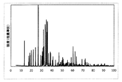
- Ba 1 Si 4 Al 3 N 9 shows a powder X-ray diffraction using the calculated CuK ⁇ ray from the crystal structure of the crystal.
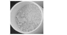
- FIG. FIG. 6 is a diagram showing the object color of the synthesized product synthesized in Example 4.
- the phosphor of the present invention includes at least an A element, a D element, an E element, and an X element (where A is one or more elements selected from Li, Mg, Ca, Sr, Ba, and La) , D is one or more elements selected from Si, Ge, Sn, Ti, Zr, and Hf, E is one or more elements selected from B, Al, Ga, In, Sc, and Y indicated elements, X is, O, N, containing at least one element) and selected from F, crystals represented by Ba 1 Si 4 Al 3 N 9 , in Ba 1 Si 4 Al 3 N 9 Inorganic crystals having the same crystal structure as the crystals to be obtained, or solid solution crystals of these crystals, M element (where M is selected from Mn, Ce, Pr, Nd, Sm, Eu, Tb, Dy, Yb 1
- the main component is an inorganic compound in which a seed or two or more elements) are dissolved.
- the crystal represented by Ba 1 Si 4 Al 3 N 9 inorganic crystals having the same crystal structure as the crystal represented by Ba 1 Si 4 Al 3 N 9 , or solid solution crystals of these crystals are generally referred to as Ba 1 Si 4 Al 3 N 9 -based crystals for simplicity.
- the crystal represented by Ba 1 Si 4 Al 3 N 9 is a crystal that has not been reported before the present invention, which was newly synthesized by the present inventor and confirmed to be a new crystal by crystal structure analysis.
- FIG. 1 is a diagram showing a crystal structure of a Ba 1 Si 4 Al 3 N 9 : Eu 2+ crystal.
- Ba 1 present inventors have synthesized Si 4 Al 3 N 9: According to the single crystal structure analysis performed on Eu 2+ crystals, Ba 1 Si 4 Al 3 N 9: Eu 2+ crystals belong to the monoclinic system, P2 It belongs to (1) / c space group (the 14th space group of International Tables for Crystallography) and occupies the crystal parameters and atomic coordinate positions shown in Table 1.
- the lattice constants a, b, and c indicate the lengths of the unit cell axes, and ⁇ , ⁇ , and ⁇ indicate the angles between the unit cell axes.
- the atomic coordinates indicate the position of each atom in the unit cell as a value between 0 and 1 with the unit cell as a unit. In this crystal, there are Ba, Si, Al, N, and Eu atoms, and Ba and Eu are present in one kind of seat (Ba, Eu (1)) without distinguishing between the seats.
- the Ba 1 Si 4 Al 3 N 9 : Eu 2+ crystal has the structure shown in FIG. 1, and a tetrahedron composed of a bond of Si or Al and N is connected. It was found that the skeleton had a structure containing Ba element. In this crystal, the M element that becomes an activating ion such as Eu is incorporated into the crystal in a form that replaces part of the Ba element.
- a 1 (D, E) 7 X 9 crystal specifically, A 1 (Si, Al) 7 (O, N) 9 crystals, more specifically A 1 Si 4 Al 3 N 9 crystals.
- a typical A element is Ba.
- a 1 (D, E) 7 X 9 crystal in the Ba 1 Si 4 Al 3 N 9 crystal, A is in the seat where Ba enters, and D and Si and Al are not distinguished from each other in the seat where Si and Al enter. X can enter the seat where E enters and N enters.
- the ratio of the number of atoms can be set to 7 for A and 1 for A and 1 for D and E, and 9 for X in total.
- the ratio of the cation of A, D, E and the anion of X satisfies the condition that the electrical neutrality in the crystal is maintained.
- Si and Al enter without distinction between the seats where Si and Al enter.
- O and N can enter the seat where N enters.
- the Ba 1 Si 4 Al 3 N 9 based crystal of the present invention can be identified by X-ray diffraction or neutron diffraction.
- a substance exhibiting the same diffraction as the X-ray diffraction result of the Ba 1 Si 4 Al 3 N 9- based crystal shown in the present invention there is a crystal represented by A 1 (D, E) 7 X 9 .
- a crystal whose lattice constant or atomic position is changed by replacing a constituent element with another element in a Ba 1 Si 4 Al 3 N 9 crystal.
- the constituent element is replaced by another element, for example, a part or all of Ba in the Ba 1 Si 4 Al 3 N 9 crystal is an A element other than Ba (where A is Li, Mg , Ca, Sr, La selected from one or more elements) and / or M element (where M is selected from Mn, Ce, Pr, Nd, Sm, Eu, Tb, Dy, Yb) Or substituted with a seed or two or more elements).
- a element other than Ba where A is Li, Mg , Ca, Sr, La selected from one or more elements
- M element where M is selected from Mn, Ce, Pr, Nd, Sm, Eu, Tb, Dy, Yb
- D element other than Si where D is one or more elements selected from Ge, Sn, Ti, Zr, and Hf.
- a part or all of Al in the crystal is substituted with E element other than Al (where E is one or more elements selected from B, Ga, In, Sc, and Y). is there. Further, there is a crystal in which part or all of N in the crystal is substituted with oxygen and / or fluorine. These substitutions are made so that the overall charge in the crystal is neutral. Those whose crystal structure does not change as a result of element substitution are Ba 1 Si 4 Al 3 N 9 -based crystals. Substitution of elements changes the light emission characteristics, chemical stability, and thermal stability of the phosphor. Therefore, it is preferable that the phosphor is selected in a timely manner according to the application within a range in which the crystal structure is maintained.
- the Ba 1 Si 4 Al 3 N 9- based crystal has a lattice constant that changes when its constituent components are replaced by other elements or when an activating element such as Eu is dissolved, but the crystal structure and atoms occupy it.
- the atomic position given by the site and its coordinates does not change so much that the chemical bond between the skeletal atoms is broken.
- Al—N and Si—N chemical bonds calculated from lattice constants and atomic coordinates obtained by Rietveld analysis of the X-ray diffraction and neutron diffraction results in the P2 (1) / c space group.
- FIG. 2 is a diagram showing powder X-ray diffraction using CuK ⁇ rays calculated from the crystal structure of Ba 1 Si 4 Al 3 N 9 crystal.
- the crystal is a Ba 1 Si 4 Al 3 N 9 -based crystal.
- the main peak of the Ba 1 Si 4 Al 3 N 9- based crystal may be determined by about 10 having strong diffraction intensity.
- Table 1 is important in that sense and serves as a reference in specifying Ba 1 Si 4 Al 3 N 9- based crystals.
- the approximate structure of the Ba 1 Si 4 Al 3 N 9 based crystal structure can be defined by using another monoclinic crystal system, in which case different space groups, lattice constants and planes can be defined. Although it is expressed using an index, the X-ray diffraction result (for example, FIG. 2) and the crystal structure (for example, FIG.
- a phosphor is obtained. Since the emission characteristics such as excitation wavelength, emission wavelength, emission intensity and the like vary depending on the composition of the Ba 1 Si 4 Al 3 N 9 based crystal and the type and amount of the activation element, it may be selected according to the application.
- At least the A element includes at least one element selected from the group consisting of Li, Mg, Ca, Sr, Ba, and La, and the D element includes Si.
- a composition containing Al in the E element, N in the X element and optionally containing O in the X element has high emission intensity.
- the luminance is particularly high when A is a mixture of Ba and Mg or Ba and Li, D is Si, E is Al, and X is N or a combination of N and O, Ba 1 Si. 4
- Ba 1 Si 4 Al 3 inorganic crystal having the same crystal structure and crystal represented by N 9 is, Ba 1 Si 4 Al 3 N 9, Mg 1 Si 4 Al 3 N 9, Ca 1 Si 4 Al 3 N 9, Sr 1 Si 4 Al 3 N 9 , La 1 Si 4 Al 3 N 9 , Li 1 Si 4 Al 3 N 9 , (Ba, Mg) 1 Si 4 Al 3 N 9 , (Ba, Ca) 1 Si 4 Al 3
- the phosphor of N 9 , (Ba, Sr) 1 Si 4 Al 3 N 9 , (Ba, La) 1 Si 4 Al 3 N 9 , or (Ba, Li) 1 Si 4 Al 3 N 9 has a crystal of It is stable and has high emission intensity.
- Inorganic crystals having the same crystal structure as those represented by Ba 1 Si 4 Al 3 N 9 are Ba 1 Si 4 -p Al 3 + p O p N 9 -p , Mg 1 Si 4 -p Al 3 + p O p N 9 -p, Ca 1 Si 4-p Al 3 + p O p N 9-p, Sr 1 Si 4-p Al 3 + p O p N 9-p, La 1 Si 4-p Al 3 + p O p N 9-p, Li 1 Si 4-p Al 3 + p O p N 9-p, (Ba, Mg) 1 Si 4-p Al 3 + p O p N 9-p, (Ba, Ca) 1 Si 4-p Al 3 + p O p N 9-p , (Ba, Sr) 1 Si 4-p Al 3 + p O p N 9-p, (Ba, La) 1 Si 4-p Al 3 + p O p N 9-p, or, (Ba, Li) 1 Si 4- p Al 3 + p O
- the activator element Eu As the activator element Eu, a phosphor with particularly high emission intensity can be obtained.
- inorganic crystals having the same crystal structure as the crystal represented by Ba 1 Si 4 Al 3 N 9 crystals in which the inorganic crystals are monoclinic are particularly stable. Is expensive.
- the inorganic crystal having the same crystal structure as that represented by Ba 1 Si 4 Al 3 N 9 is a monoclinic crystal, has symmetry of the space group P2 (1) / c, and has a lattice constant.
- the crystals are particularly stable, and the phosphors using these as host crystals have high emission intensity. Outside this range, the crystal becomes unstable and the light emission intensity may decrease.
- A is one or more elements selected from Li, Mg, Ca, Sr, Ba, La, D is Si, Ge, Sn, Ti, Zr, One or more elements selected from Hf, E is one or more elements selected from B, Al, Ga, In, Sc, and Y, and X is selected from O, N, and F
- One or more elements) and the parameters d, e, f, g, h are 0.00001 ⁇ d ⁇ 0.05 0.01 ⁇ e ⁇ 0.07 0.10 ⁇ f ⁇ 0.30 0.10 ⁇ g ⁇ 0.30 0.45 ⁇ h ⁇ 0.65
- a phosphor that satisfies all of the above conditions has particularly high emission intensity.
- the parameter d is the addition amount of the activator element. If it is less than 0.00001, the amount of luminescent ions may be insufficient and the luminance may decrease. If the parameter d is more than 0.05, the emission intensity may decrease due to concentration quenching due to the interaction between the luminescent ions.
- the parameter e is a parameter representing the composition of an A element such as Ba, and if it is less than 0.01 or higher than 0.07, the crystal structure may become unstable and the emission intensity may decrease.
- the parameter f is a parameter representing the composition of the D element such as Si, and if it is less than 0.10 or higher than 0.3, the crystal structure may become unstable and the light emission intensity may decrease.
- the parameter g is a parameter representing the composition of an E element such as Al, and if it is less than 0.10 or higher than 0.3, the crystal structure may become unstable and the light emission intensity may decrease.
- the parameter h is a parameter representing the composition of the X element such as O, N, F, etc. If it is less than 0.45 or higher than 0.65, the crystal structure may become unstable and the emission intensity may decrease.
- the X element is an anion, and the composition of the O, N, and F ratios can be determined so that the cation of the A, M, D, and E elements and the neutral charge are maintained.
- parameters f and g are 0/7 ⁇ f / (f + g) ⁇ 7/7 A composition satisfying the above condition has a stable crystal structure and high emission intensity. More preferably, the parameters f and g are 2/7 ⁇ f / (f + g) ⁇ 4/7 A composition satisfying the above condition can be expected to have a more stable crystal structure and higher emission intensity.
- the X element contains N and O
- a composition satisfying the above condition has a stable crystal structure and high emission intensity. More preferably, the parameters h1 and h2 are 0/9 ⁇ h1 / (h1 + h2) ⁇ 2/9
- a composition satisfying the above condition can be expected to have a more stable crystal structure and higher emission intensity.
- a phosphor containing at least Eu as an M element as an activator is a phosphor having a high emission intensity in the present invention, and a blue to green phosphor can be obtained with a specific composition.
- the composition containing at least Ba as the A element, containing at least Si as the D element, containing at least Al as the E element, and containing at least N as the X element has a stable crystal structure and a light emission intensity. high.
- boron may be included as the E element.
- the boron content is 0.001% by mass or more and 1% by mass or less. Thereby, the light emission intensity can be increased.
- a phosphor containing an inorganic compound which is a single crystal particle having an average particle diameter of 0.1 ⁇ m or more and 20 ⁇ m or less or an aggregate of single crystal particles has high luminous efficiency and good operability when mounted on an LED.
- the particle size should be controlled.
- the impurity elements of Fe, Co, and Ni contained in the inorganic compound may cause a decrease in emission intensity.
- the total of these elements in the phosphor is 500 ppm or less, the influence of the decrease in emission intensity is reduced.
- the phosphor of the present invention is different from this in addition to an inorganic compound having a Ba 1 Si 4 Al 3 N 9- based crystal as a base material and an activating ion M dissolved therein.
- a phosphor that further contains another crystal phase or an amorphous phase and has an inorganic compound content of 20% by mass or more.
- the present embodiment may be used when a desired characteristic cannot be obtained with a Ba 1 Si 4 Al 3 N 9- based crystal alone or when a function such as conductivity is added.
- the content of the Ba 1 Si 4 Al 3 N 9 based crystal may be adjusted according to the intended characteristics, but if it is 20% by mass or less, the emission intensity may be lowered. From such a viewpoint, in the phosphor of the present invention, 20% by mass or more is preferably used as a main component of the above-described inorganic compound.
- the phosphor When the phosphor is required to have conductivity such as for electron beam excitation, it is preferable to add an inorganic substance having conductivity as another crystal phase or amorphous phase.
- the inorganic substance having conductivity examples include an oxide, an oxynitride, a nitride, or a mixture thereof containing one or more elements selected from Zn, Al, Ga, In, and Sn. it can.
- zinc oxide, aluminum nitride, indium nitride, tin oxide, and the like can be given.
- a second other phosphor may be added.
- Other phosphors include BAM phosphor, ⁇ -sialon phosphor, ⁇ -sialon phosphor, (Sr, Ba) 2 Si 5 N 8 phosphor, CaAlSiN 3 phosphor, (Ca, Sr) AlSiN 3 phosphor
- inorganic phosphors such as The other crystalline phase or amorphous phase may be the above-described inorganic phosphor.
- a phosphor having a peak at a wavelength in a range of 450 nm to 530 nm when irradiated with an excitation source.
- a Ba 1 Si 4 Al 3 N 9- based crystal phosphor activated with Eu has a light emission peak in this range by adjusting the composition.
- a phosphor that emits light with vacuum ultraviolet rays, ultraviolet rays, visible light, electron beams, or X-rays having an excitation source with a wavelength of 100 nm to less than 450 nm.
- an excitation source with a wavelength of 100 nm to less than 450 nm.
- One embodiment of the present invention is a phosphor in which Eu is dissolved in an inorganic crystal having the same crystal structure as that represented by Ba 1 Si 4 Al 3 N 9 .
- an inorganic crystal having the same crystal structure as that represented by Ba 1 Si 4 Al 3 N 9 By adjusting the composition, when irradiating light of 280 nm or more and 405 nm or less, blue to green fluorescence of 450 nm or more and 530 nm or less is emitted. Therefore, it is preferable to use for blue to green light emission such as a white LED.
- the color emitted when the excitation source is irradiated is a value of (x, y) on the CIE1931 chromaticity coordinates, 0 ⁇ x ⁇ 0.4 0 ⁇ y ⁇ 0.9
- phosphors For example, Eu q Ba 1-q Si 4-p Al 3 + p N 9-p O p However, 0 ⁇ p ⁇ 4 0.0001 ⁇ q ⁇ 1
- a phosphor that develops a color having a chromaticity coordinate in this range can be obtained. It is good to use for blue to green light emission such as white LED.
- the phosphor of the present invention has a wide excitation range from electron beam, X-ray, and ultraviolet light to visible light, and in particular, exhibits a blue to green color of 450 nm or more and 530 nm or less, and an emission wavelength.
- the emission peak width is adjustable. Therefore, the phosphor of the present invention is suitable for a lighting fixture and an image display device due to such light emission characteristics.
- the phosphor of the present invention is also superior in heat resistance because it does not deteriorate even when exposed to high temperatures, and also has the advantage of excellent long-term stability in an oxidizing atmosphere and moisture environment. Products with excellent properties can be provided.
- a method for producing such a phosphor of the present invention is not particularly defined.
- it is a mixture of metal compounds, and a Ba 1 Si 4 Al 3 N 9- based crystal is converted into a base crystal by firing, and attached thereto. It can be obtained by firing a raw material mixture capable of constituting an inorganic compound in which the active ions M are dissolved in a temperature range of 1200 ° C. to 2200 ° C. in an inert atmosphere containing nitrogen.
- the main crystal of the present invention is monoclinic and belongs to the space group P2 (1) / c, crystals having a different crystal system or space group may be mixed depending on the synthesis conditions such as the firing temperature. Even in this case, since the change in the light emission characteristics is slight, it can be used as a high-luminance phosphor.
- a mixture of metal compounds is a compound containing M, a compound containing A, a compound containing D, a compound containing E, and a compound containing X
- M Is one or more elements selected from Mn, Ce, Pr, Nd, Sm, Eu, Tb, Dy, Yb
- A is one selected from Li, Mg, Ca, Sr, Ba, La Or, two or more elements
- D is one or more elements selected from Si, Ge, Sn, Ti, Zr, and Hf
- E is selected from B, Al, Ga, In, Sc, and Y It is preferable to use one or more elements
- X is one or more elements selected from O, N, and F).
- the compound containing M is a simple substance or two kinds selected from metals containing M, silicides, oxides, carbonates, nitrides, oxynitrides, chlorides, fluorides, or oxyfluorides A mixture of the above, wherein the compound containing A is a simple substance selected from metals containing A, silicides, oxides, carbonates, nitrides, oxynitrides, chlorides, fluorides, or oxyfluorides, or A compound containing two or more kinds and containing D is selected from metals containing D, silicides, oxides, carbonates, nitrides, oxynitrides, chlorides, fluorides, or oxyfluorides A simple substance or a mixture of two or more, and a compound containing E is selected from a metal, silicide, oxide, carbonate, nitride, oxynitride, chloride, fluoride, or oxyfluoride containing E Single substance or mixture
- the furnace used for firing has a high firing temperature, and the firing atmosphere is an inert atmosphere containing nitrogen. Therefore, carbon is used as a material for the high-temperature part of the furnace in a metal resistance heating method or a graphite resistance heating method. A suitable electric furnace is preferred.
- the pressure range of the inert atmosphere containing nitrogen is preferably in the range of 0.1 MPa to 100 MPa because the thermal decomposition of the starting material and the product nitride or oxynitride is suppressed.
- the inert atmosphere containing nitrogen is preferably a nitrogen gas atmosphere.
- the oxygen partial pressure in the firing atmosphere is preferably 0.0001% or less in order to suppress the oxidation reaction of the starting material and the product nitride or oxynitride.
- the firing time varies depending on the firing temperature, but is usually about 1 to 10 hours.
- the relative bulk density is a ratio of a value (bulk density) obtained by dividing the mass of the powder filled in the container by the volume of the container and the true density of the substance of the powder. Unless otherwise specified, in the present invention, the relative bulk density is simply referred to as bulk density.
- boron or boron nitride components are mixed from the container into the product, but if the amount is small, the light emission characteristics are not deteriorated, so the influence is small. Furthermore, the addition of a small amount of boron nitride may improve the durability of the product, which is preferable in some cases.
- the shape of the mixture of metal compounds is powder or aggregate, and if the average particle diameter is 500 ⁇ m or less, the reactivity and operability are excellent. preferable.
- the particle size of the particles or aggregates As a method of setting the particle size of the particles or aggregates to 500 ⁇ m or less, it is preferable to use a spray dryer, sieving, or air classification because the work efficiency and operability are excellent.
- a firing method in which mechanical pressure is not applied from the outside of the atmospheric pressure sintering method or the gas pressure sintering method without using hot pressing is preferable.
- the average particle diameter of the phosphor powder is preferably from 50 nm to 200 ⁇ m in terms of volume-based median diameter (d50) because the emission intensity is high.
- the volume-based average particle diameter can be measured by, for example, a microtrack or a laser scattering method.
- the average particle size of the phosphor powder synthesized by firing may be adjusted to 50 nm to 200 ⁇ m.
- Defects contained in the powder and damage due to pulverization by heat-treating the phosphor powder after firing, the phosphor powder after pulverization treatment, or the phosphor powder after particle size adjustment at a temperature of 1000 ° C. or more and below the firing temperature May recover. Defects and damage may cause a decrease in emission intensity, and the emission intensity is restored by heat treatment.
- an inorganic compound that generates a liquid phase may be added at a temperature lower than the firing temperature and fired.
- An inorganic compound that generates such a liquid phase acts as a flux, and reaction and grain growth may be promoted to obtain a stable crystal, which may improve the emission intensity.
- the content of the inorganic compound that forms a liquid phase at a temperature lower than the firing temperature is reduced. This may increase the emission intensity of the phosphor.
- the phosphor of the present invention When the phosphor of the present invention is used for a light emitting device or the like, it is preferable to use the phosphor in a form dispersed in a liquid medium. Moreover, it can also be used as a phosphor mixture containing the phosphor of the present invention.
- the phosphor of the present invention dispersed in a liquid medium is called a phosphor-containing composition.
- the liquid medium that can be used in the phosphor-containing composition of the present invention is a liquid medium that exhibits liquid properties under the desired use conditions, suitably disperses the phosphor of the present invention, and does not cause undesirable reactions. If there is, it is possible to select an arbitrary one according to the purpose.
- the liquid medium include addition-reactive silicone resins, condensation-reactive silicone resins, modified silicone resins, epoxy resins, polyvinyl resins, polyethylene resins, polypropylene resins, and polyester resins before curing. These liquid media may be used individually by 1 type, and may use 2 or more types together by arbitrary combinations and a ratio.
- the amount of the liquid medium used may be appropriately adjusted according to the application, etc., but in general, the weight ratio of the liquid medium to the phosphor of the present invention is usually 3% by weight or more, preferably 5% by weight or more, Moreover, it is 30 weight% or less normally, Preferably it is the range of 15 weight% or less.
- the phosphor-containing composition of the present invention may contain other arbitrary components in addition to the phosphor of the present invention and a liquid medium, depending on its use and the like.
- examples of other components include a diffusing agent, a thickener, a bulking agent, and an interference agent.
- silica-based fine powder such as Aerosil, alumina and the like can be mentioned.
- the light emitting device of the present invention includes at least a light emitter or a light emitting light source and a phosphor, and the phosphor includes at least the phosphor of the present invention described above.
- Examples of the light emitter or light source include a light emitting diode (LED) light emitting device, a laser diode (LD) light emitting device, a semiconductor laser, an organic EL light emitting device (OLED), and a fluorescent lamp.
- LED light emitting diode
- LD laser diode
- OLED organic EL light emitting device
- An LED light emitting device can be manufactured by using the phosphor of the present invention by a known method as described in JP-A-5-152609, JP-A-7-99345, JP-A-2927279, and the like. In this case, it is desirable that the light emitter or the light source emits light having a wavelength of 280 nm to less than 450 nm.
- an ultraviolet (or purple) LED light emitting element having a wavelength of 280 nm to 405 nm or a blue LED light emitting element having a wavelength of 405 nm to 450 nm is preferable.
- Some of these LED light-emitting elements are made of a nitride semiconductor such as GaN or InGaN. By adjusting the composition, the LED light-emitting element can be a light-emitting light source that emits light of a predetermined wavelength.
- Examples of the light emitting device of the present invention include a white light emitting diode, a lighting fixture including a plurality of white light emitting diodes, a backlight for a liquid crystal panel, and the like including the phosphor of the present invention.
- Eu-activated ⁇ -sialon phosphor in addition to the phosphor of the present invention, Eu-activated ⁇ -sialon phosphor, Eu-activated ⁇ -sialon yellow phosphor, Eu-activated Sr 2 Si 5 N 8
- One or more phosphors selected from orange phosphors, Eu-activated (Ca, Sr) AlSiN 3 orange phosphors, and Eu-activated CaAlSiN 3 red phosphors may be further included.
- yellow phosphors other than the above for example, YAG: Ce, (Ca, Sr, Ba) Si 2 O 2 N 2 : Eu, or the like may be used.
- the light emitting body or light emitting light source emits ultraviolet or visible light having a peak wavelength of 280 nm or more and less than 450 nm, and the phosphor of the present invention emits blue to green light, and other phosphors of the present invention.
- a light-emitting device that emits white light or light other than white light by mixing with light having a wavelength of 450 nm or more emitted by.
- a blue phosphor that emits light having a peak wavelength of 420 nm or more and 500 nm or less by a light emitter or a light source can be included.
- Such blue phosphors include AlN: (Eu, Si), BaMgAl 10 O 17 : Eu, SrSi 9 Al 19 ON 31 : Eu, LaSi 9 Al 19 N 32 : Eu, ⁇ -sialon: Ce, JEM : Ce and the like.
- a green phosphor that emits light having a peak wavelength of 500 nm or more and 550 nm or less by a light emitting body or a light emitting light source can be included.
- examples of such green phosphors include ⁇ -sialon: Eu, (Ba, Sr, Ca, Mg) 2 SiO 4 : Eu, (Ca, Sr, Ba) Si 2 O 2 N 2 : Eu, and the like. is there.
- a yellow phosphor that emits light having a peak wavelength of 550 nm or more and 600 nm or less by a light emitter or a light source can be included.
- Examples of such a yellow phosphor include YAG: Ce, ⁇ -sialon: Eu, CaAlSiN 3 : Ce, La 3 Si 6 N 11 : Ce.
- a red phosphor that emits light having a peak wavelength of 600 nm or more and 700 nm or less by a light emitter or a light source can be included.
- red phosphor include CaAlSiN 3 : Eu, (Ca, Sr) AlSiN 3 : Eu, Ca 2 Si 5 N 8 : Eu, and Sr 2 Si 5 N 8 : Eu.
- the light-emitting device of the present invention when an LED that emits light having a wavelength of 280 nm or more and less than 450 nm is used as a light-emitting body or a light-emitting light source, the light-emitting efficiency is high.
- the image display device of the present invention includes at least an excitation source and a phosphor, and the phosphor includes at least the phosphor of the present invention described above.
- Examples of the image display device include a fluorescent display tube (VFD), a field emission display (FED), a plasma display panel (PDP), a cathode ray tube (CRT), and a liquid crystal display (LCD).
- VFD fluorescent display tube
- FED field emission display
- PDP plasma display panel
- CRT cathode ray tube
- LCD liquid crystal display
- the phosphor of the present invention has been confirmed to emit light by excitation of vacuum ultraviolet rays of 100 to 190 nm, ultraviolet rays of 190 to 380 nm, electron beams, etc., and in combination of these excitation sources and the phosphor of the present invention, An image display apparatus as described above can be configured.
- the phosphor of the present invention which is mainly composed of an inorganic compound having a specific chemical composition, can be used as a pigment or a fluorescent pigment because it has a white object color. That is, when the phosphor of the present invention is irradiated with illumination such as sunlight or a fluorescent lamp, a white object color is observed, but the color development is good and the phosphor of the present invention does not deteriorate for a long time. Is suitable for inorganic pigments. For this reason, when used for paints, inks, paints, glazes, colorants added to plastic products, etc., good color development can be maintained high over a long period of time.
- the phosphor of the present invention absorbs ultraviolet rays and is therefore suitable as an ultraviolet absorber. For this reason, when used as a paint, applied to the surface of a plastic product, or kneaded into a plastic product, the effect of blocking ultraviolet rays is high, and the product can be effectively protected from ultraviolet degradation.
- the raw material powder used in the synthesis was a silicon nitride powder having a specific surface area of 11.2 m 2 / g, an oxygen content of 1.29 wt%, and an ⁇ -type content of 95% (SN-E10 manufactured by Ube Industries, Ltd.).
- Silicon nitride (Si 3 N 4 ), barium nitride (Ba 3 N 2 ), aluminum nitride (AlN) and europium nitride (EuN) are mixed at a molar ratio of 1.33: 0.33: 3: 0.02.
- the composition was designed. These raw material powders were weighed so as to have the above mixed composition, and mixed for 5 minutes using a silicon nitride sintered body pestle and mortar. Next, the obtained mixed powder was put into a crucible made of a boron nitride sintered body. The bulk density of the mixed powder (powder) was about 30%.
- the crucible containing the mixed powder was set in a graphite resistance heating type electric furnace.
- the firing operation is as follows. First, the firing atmosphere is set to a vacuum of 1 ⁇ 10 ⁇ 1 Pa or less with a diffusion pump, heated from room temperature to 800 ° C. at a rate of 500 ° C. per hour, and at 800 ° C. the purity is 99.999% by volume. Nitrogen was introduced to bring the pressure in the furnace to 1 MPa, and the temperature was raised to 2000 ° C. at 500 ° C. per hour and held at that temperature for 2 hours.
- the synthesized product was observed with an optical microscope, and crystal particles having a size of 80 ⁇ m ⁇ 50 ⁇ m ⁇ 3 ⁇ m were collected from the synthesized product.
- the particles were analyzed using a scanning electron microscope (SEM; SU1510 manufactured by Hitachi High-Technologies Corporation) equipped with an energy dispersive element analyzer (EDS; QUANTAX manufactured by Bruker AXS). Analysis was carried out. As a result, the presence of Ba, Si, Al, N, and Eu elements was confirmed, and the ratio of the number of Ba, Si, and Al contained atoms was measured to be 1: 4: 3.
- this crystal was fixed to the tip of the glass fiber with an organic adhesive.
- a single crystal X-ray diffractometer with a rotating counter cathode of MoK ⁇ rays (SMART APEXII Ultra manufactured by Bruker AXS Co., Ltd.) was used to perform X-ray diffraction measurement under the condition that the output of the X-ray source was 50 kV 50 mA. .
- the crystal particles were a single crystal.
- the crystal structure was determined from the X-ray diffraction measurement result using single crystal structure analysis software (APEX2 manufactured by Bruker AXS).
- the obtained crystal structure data is shown in Table 1, and a diagram of the crystal structure is shown in FIG. Table 1 describes the crystal system, space group, lattice constant, atom type and atom position, and this data can be used to determine the shape and size of the unit cell and the arrangement of atoms in it. .
- Si and Al enter at the same atomic position, and oxygen and nitrogen enter at the same atomic position, and when they are averaged as a whole, the composition ratio of the crystal is obtained.
- the atomic positions are as shown in Table 1.
- Si and Al are present at a certain ratio determined by the composition at the same atomic position. In general, oxygen and nitrogen can enter the seat where X enters in a sialon-based crystal.
- Ba 1 Si 4 Al 3 N 9 crystals can replace part or all of Ba with Li, Mg, Ca, Sr or La while maintaining the crystal structure. That is, the crystal of A 1 Si 4 Al 3 N 9 (A is one or two selected from Li, Mg, Ca, Sr, Ba, and La) has the same crystal structure as the Ba 1 Si 4 Al 3 N 9 crystal have. Further, a part of Si can be replaced with Al, a part of Al can be replaced with Si, and a part of N can be replaced with oxygen. This crystal has the same crystal structure as Ba 1 Si 4 Al 3 N 9. It was confirmed to be one composition of the crystal group.
- FIG. 2 is a diagram showing powder X-ray diffraction using CuK ⁇ rays calculated from the crystal structure of Ba 1 Si 4 Al 3 N 9 : Eu 2+ .
- the raw materials were weighed so as to have the raw material mixture composition (mass ratio) shown in Table 4.
- the composition may differ between the design composition in Tables 2 and 3 and the raw material mixture composition in Table 4.
- the raw material mixture composition was determined so that the amount of metal ions matched.
- the weighed raw material powder was mixed for 5 minutes using a silicon nitride sintered pestle and mortar to obtain a raw material mixture which is a mixture of metal compounds. Thereafter, the raw material mixture of the powder was put into a crucible made of a boron nitride sintered body. The bulk density of the powder was about 20% to 30%.
- the crucible containing the raw material mixture was set in a graphite resistance heating type electric furnace.
- the firing operation is as follows. First, the firing atmosphere is set to a vacuum of 1 ⁇ 10 ⁇ 1 Pa or less with a diffusion pump, heated from room temperature to 800 ° C. at a rate of 500 ° C. per hour, and at 800 ° C. the purity is 99.999% by volume. Nitrogen was introduced to bring the pressure in the furnace to 1 MPa, the temperature was raised to 500 ° C. per hour to the set temperature shown in Table 5, and the temperature was maintained for 2 hours.
- the synthesized compound was pulverized using an agate mortar, and powder X-ray diffraction measurement was performed using Cu K ⁇ rays.
- the main product phase is shown in Table 6.
- the composites of Examples 2 to 11 contained rare earth elements, alkaline earth metals, Si, Al, and N, and the composites of Examples 12 to 14 were rare earth elements, alkaline earth metals, It was confirmed that Si, Al, O and N were contained.
- Li was analyzed using the mass spectrum.
- the composite material is irradiated with laser light having a beam diameter of 30 ⁇ m and a wavelength of 213 nm by a Nd: YAG laser manufactured by New Wave Research, and the Li element volatilized from the composite is subjected to ICP mass spectrum attached to laser ablation. Analyzed by meter.
- the X-ray diffraction patterns of the composites of all the examples are in good agreement with the X-ray diffraction patterns of Ba 1 Si 4 Al 3 N 9 : Eu 2+ by the structural analysis shown in FIG. 2, and Ba 1 Si 4 Al 3 N It was confirmed that a crystal having the same crystal structure as 9 crystals was the main component.
- the composite of the example of the present invention contains a phase having the same crystal structure as the crystal represented by Ba 1 Si 4 Al 3 N 9 as a main product phase, containing 20% by mass or more. Confirmed that it will be.
- Example 4 it was confirmed from the measurement of EDS that the composite contained Eu, Ba, Mg, Si, Al, and N. Moreover, it was confirmed that the ratio of Eu: Ba: Mg: Si: Al was 0.1: 0.5: 0.4: 4: 3.
- the impurity second phase is mixed in the synthesized product.
- the composite of the example of the present invention was an inorganic compound in which an activating element M such as Eu was dissolved in a Ba 1 Si 4 Al 3 N 9 system crystal.
- the obtained composite (fired body) was coarsely pulverized and then manually pulverized using a silicon nitride sintered crucible and a mortar, and passed through a 30 ⁇ m sieve.
- the average particle size was 3 to 8 ⁇ m.
- FIG. 3 is a diagram showing an excitation spectrum and an emission spectrum of the synthesized product synthesized in Example 4.
- Example 4 it was found that the synthesized product of Example 4 could be excited most efficiently at 324 nm, and the emission spectrum when excited at 324 nm emitted blue light having a peak at 477 nm. In addition, it was confirmed that the emission color of the phosphor of Example 4 was in the range of 0 ⁇ x ⁇ 0.4 and 0 ⁇ y ⁇ 0.9 in the CIE1931 chromaticity coordinates.
- the composite of the present invention is a phosphor that can be excited by ultraviolet rays of 250 nm to 380 nm, violet or blue light of 380 nm to 450 nm, and emits blue to green light. .
- the composite of the example of the present invention is an inorganic compound in which an activating element M such as Eu is dissolved in a Ba 1 Si 4 Al 3 N 9- based crystal, and this inorganic compound is a phosphor.
- an activating element M such as Eu
- this inorganic compound is a phosphor.
- FIG. 4 is a diagram showing the object color of the synthesized product synthesized in Example 4.
- Example 4 had a white object color and was excellent in color development.
- the composite obtained in Example 4 has a white object color and was excellent in color development.
- it is shown in black and white due to restrictions on application documents, but the original is in color, and a color diagram can be submitted upon request.
- the composites of other examples also showed similar object colors.
- the inorganic compound, which is the composite of the present invention can be used as a pigment or a fluorescent pigment because it exhibits a white object color upon irradiation with illumination such as sunlight or a fluorescent lamp.
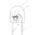
- FIG. 5 is a schematic view showing a lighting fixture (bullet type LED lighting fixture) according to the present invention.
- a so-called bullet-type white light-emitting diode lamp (1) shown in FIG. 5 was produced.
- the phosphor (7) is dispersed in the resin and mounted in the vicinity of the ultraviolet light emitting diode element (4).
- the first resin (6) in which the phosphor is dispersed is transparent and covers the entire ultraviolet light emitting diode element (4).
- the tip of the lead wire including the recess, the ultraviolet light emitting diode element, and the first resin in which the phosphor is dispersed are sealed with a transparent second resin (8).
- the transparent second resin (8) has a substantially cylindrical shape as a whole, and has a lens-shaped curved surface at the tip, which is commonly called a shell type.
- a phosphor powder obtained by mixing the blue phosphor produced in Example 4, the green phosphor produced in Example 14, and the red phosphor represented by CaAlSiN 3 : Eu was used at a concentration of 35% by weight.
- the mixture was mixed with an epoxy resin, and an appropriate amount thereof was dropped using a dispenser to form a first resin (6) in which a mixture of phosphors (7) was dispersed.
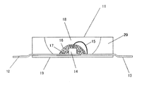
- FIG. 6 is a schematic view showing a lighting fixture (substrate mounted LED lighting fixture) according to the present invention.
- a chip-type white light emitting diode lamp (11) for board mounting shown in FIG. 6 was produced.
- Two lead wires (12, 13) are fixed to a white alumina ceramic substrate (19) having a high visible light reflectivity, and one end of each of these wires is located at a substantially central portion of the substrate, and the other end is external. It is an electrode that is soldered when mounted on an electric board.
- One of the lead wires (12) has a violet light emitting diode element (14) having an emission peak wavelength of 405 nm placed and fixed at one end of the lead wire so as to be in the center of the substrate.
- the lower electrode of the purple light emitting diode element (14) and the lower lead wire are electrically connected by a conductive paste, and the upper electrode and the other lead wire (13) are bonding wires (gold wires) 15) is electrically connected.
- a mixture of the first resin (16) and the phosphor (17) obtained by mixing the blue phosphor prepared in Example 4 and the yellow phosphor represented by ⁇ -sialon: Eu is in the vicinity of the light emitting diode element.
- the first resin in which the phosphor is dispersed is transparent and covers the entire purple light emitting diode element (14).
- a wall surface member (20) having a shape with a hole in the center is fixed on the ceramic substrate.
- the wall member (20) has a hole in the center for accommodating the resin (16) in which the violet light-emitting diode element (14) and the phosphor (17) are dispersed. It has become.
- This slope is a reflection surface for extracting light forward, and the curved surface shape of the slope is determined in consideration of the light reflection direction. Further, at least the surface constituting the reflecting surface is a surface having a high visible light reflectance having white or metallic luster.
- the wall member (20) is made of a white silicone resin. The hole at the center of the wall member forms a recess as the final shape of the chip-type light-emitting diode lamp.
- the first resin (14) in which the purple light-emitting diode element (14) and the phosphor (17) are dispersed A transparent second resin (18) is filled so as to seal all of 16).
- the same epoxy resin was used for the first resin (16) and the second resin (18). The achieved chromaticity and the like are substantially the same as in Example 15.
- FIG. 7 is a schematic view showing an image display device (plasma display panel) according to the present invention.
- the red phosphor (CaAlSiN 3 : Eu) (31), the green phosphor (32) produced in Example 14 and the blue phosphor (33) produced in Example 4 were placed on the glass substrate (44) on the electrode ( 37, 38, 39) and the inner surface of each cell (34, 35, 36) disposed via the dielectric layer (41).
- the electrodes (37, 38, 39, 40) are energized, vacuum ultraviolet rays are generated by Xe discharge in the cell, which excites the phosphor and emits red, green, and blue visible light, which is the protective layer. (43), observed from the outside through the dielectric layer (42) and the glass substrate (45), and functions as an image display device.
- FIG. 8 is a schematic view showing an image display device (field emission display panel) according to the present invention.
- the blue phosphor (56) produced in Example 4 of the present invention is applied to the inner surface of the anode (53).
- a voltage between the cathode (52) and the gate (54) electrons (57) are emitted from the emitter (55).
- the electrons are accelerated by the voltage of the anode (53) and the cathode, collide with the blue phosphor (56), and the phosphor emits light.
- the whole is protected by glass (51).
- the figure shows one light-emitting cell consisting of one emitter and one phosphor, but in reality, a display that can produce a variety of colors is constructed by arranging a number of red and green cells in addition to blue.
- the phosphor used for the green or red cell is not particularly specified, but a phosphor that emits high luminance with a low-speed electron beam may be used.
- the phosphor of the present invention has emission characteristics (emission color, excitation characteristics, emission spectrum) different from those of conventional phosphors, and has high emission intensity even when combined with an LED of less than 450 nm.
- the phosphor is suitable for use in VFD, FED, PDP, CRT, white LED, LCD, and the like because the phosphor is less stable when exposed to an excitation source. In the future, it can be expected to contribute greatly to the development of the industry in material design for various display devices.
Landscapes
- Chemical & Material Sciences (AREA)
- Organic Chemistry (AREA)
- Inorganic Chemistry (AREA)
- Engineering & Computer Science (AREA)
- Materials Engineering (AREA)
- Health & Medical Sciences (AREA)
- Chemical Kinetics & Catalysis (AREA)
- Medicinal Chemistry (AREA)
- Polymers & Plastics (AREA)
- Luminescent Compositions (AREA)
- Pigments, Carbon Blacks, Or Wood Stains (AREA)
- Led Device Packages (AREA)
Abstract
Description
前記Ba1Si4Al3N9で示される結晶と同一の結晶構造を有する無機結晶は、A1(D,E)7X9で示される結晶であり、少なくとも、A元素にLi、Mg、Ca、Sr、BaおよびLaからなる群から少なくとも1つ選択される元素を含み、D元素にSiを含み、E元素にAlを含み、X元素にNを含み、必要に応じてX元素にOを含んでもよい。
前記Ba1Si4Al3N9で示される結晶と同一の結晶構造を有する無機結晶は、Ba1Si4Al3N9、Mg1Si4Al3N9、Ca1Si4Al3N9、Sr1Si4Al3N9、La1Si4Al3N9、Li1Si4Al3N9、(Ba,Mg)1Si4Al3N9、(Ba,Ca)1Si4Al3N9、(Ba,Sr)1Si4Al3N9、(Ba,La)1Si4Al3N9、または、(Ba,Li)1Si4Al3N9であってもよい。
前記Ba1Si4Al3N9で示される結晶と同一の結晶構造を有する無機結晶は、Ba1Si4-pAl3+pOpN9-p、Mg1Si4-pAl3+pOpN9-p、Ca1Si4-pAl3+pOpN9-p、Sr1Si4-pAl3+pOpN9-p、La1Si4-pAl3+pOpN9-p、Li1Si4-pAl3+pOpN9-p、(Ba,Mg)1Si4-pAl3+pOpN9-p、(Ba,Ca)1Si4-pAl3+pOpN9-p、(Ba,Sr)1Si4-pAl3+pOpN9-p、(Ba,La)1Si4-pAl3+pOpN9-p、または、(Ba,Li)1Si4-pAl3+pOpN9-p(ただし、0 ≦ p < 4)の組成式で示されてもよい。
前記M元素はEuであってもよい。
前記Ba1Si4Al3N9で示される結晶と同一の結晶構造を有する無機結晶は、単斜晶系の結晶であってもよい。
前記Ba1Si4Al3N9で示される結晶と同一の結晶構造を有する無機結晶は、単斜晶系の結晶であり、空間群P2(1)/cの対称性を持ち、
格子定数a、b、cは、
a = 0.58465±0.05 nm
b = 2.67255±0.05 nm
c = 0.58386±0.05 nm
の範囲の値であってもよい。
前記無機化合物は、組成式MdAeDfEgXh(ただし、式中d+e+f+g+h = 1であり、Mは、Mn、Ce、Pr、Nd、Sm、Eu、Tb、Dy、Ybから選ばれる1種または2種以上の元素、Aは、Li、Mg、Ca、Sr、Ba、Laから選ばれる1種または2種以上の元素、Dは、Si、Ge、Sn、Ti、Zr、Hfから選ばれる1種または2種以上の元素、Eは、B、Al、Ga、In、Sc、Yから選ばれる1種または2種以上の元素、Xは、O、N、Fから選ばれる1種または2種以上の元素)で示され、パラメータd、e、f、g、hは、
0.00001 ≦ d ≦ 0.05
0.01 ≦ e ≦ 0.07
0.10 ≦ f ≦ 0.30
0.10 ≦ g ≦ 0.30
0.45 ≦ h ≦ 0.65
の条件を全て満たす範囲の組成で表されてもよい。
前記パラメータd、e、f、g、hは、
d+e = (1/17)±0.05
f+g = (7/17)±0.05
h = (9/17)±0.05
の条件を全て満たす範囲の値であってもよい。
前記パラメータf、gは、
0/7 ≦ f/(f+g) ≦ 7/7
の条件を満たしてもよい。
前記X元素はOとNとを含み、前記無機化合物は、組成式MdAeDfEgOh1Nh2(ただし、式中d+e+f+g+h1+h2 = 1、および、h1+h2 = hである)で示され、
0/9 ≦ h1/(h1+h2) ≦ 6/9
の条件を満たしてもよい。
前記M元素として少なくともEuを含んでもよい。
前記A元素として少なくともBaを含み、前記D元素として少なくともSiを含み、前記E元素として少なくともAlを含み、前記X元素として少なくともNを含んでもよい。
前記無機化合物の組成式はパラメータpとqとを用いて
EuqBa1-qSi4-pAl3+pN9-pOp
ただし、
0 ≦ p < 4
0.0001 ≦ q < 1
で示されてもよい。
前記無機化合物は、平均粒径0.1μm以上20μm以下の単結晶粒子あるいは前記単結晶粒子の集合体であってもよい。
前記無機化合物に含まれる、Fe、Co、Ni不純物元素の合計が500ppm以下であってもよい。
前記無機化合物に加えて、前記無機化合物とは異なる他の結晶相あるいはアモルファス相をさらに含み、前記無機化合物の含有量は20質量%以上であってもよい。
前記他の結晶相あるいはアモルファス相は、導電性を持つ無機物質であってもよい。
前記導電性を持つ無機物質は、Zn、Al、Ga、In、Snから選ばれる1種または2種以上の元素を含む酸化物、酸窒化物、窒化物、あるいは、これらの混合物であってもよい。
前記他の結晶相あるいはアモルファス相は、前記蛍光体とは異なる無機蛍光体であってもよい。
励起源を照射することにより450nm以上530nm以下の範囲の波長にピークを持つ蛍光を発光してもよい。
前記励起源は、100nm以上450nm未満の波長を持つ真空紫外線、紫外線または可視光、電子線またはX線であってもよい。
280nm以上405nm以下の光を照射すると450nm以上530nm以下の青色から緑色の蛍光を発してもよい。
励起源が照射されたときに発光する色がCIE1931色度座標上の(x,y)の値で、
0 ≦ x ≦ 0.4
0 ≦ y ≦ 0.9
の条件を満たしてもよい。
本発明による上記蛍光体の製造方法は、金属化合物の混合物であって焼成することにより、上記無機化合物を構成しうる原料混合物を、窒素を含有する不活性雰囲気中において1200℃以上2200℃以下の温度範囲で焼成し、これにより上記課題を解決する。
前記金属化合物の混合物は、Mを含有する化合物と、Aを含有する化合物と、Dを含有する化合物と、Eを含有する化合物と、Xを含有する化合物(ただし、Mは、Mn、Ce、Pr、Nd、Sm、Eu、Tb、Dy、Ybから選ばれる1種または2種以上の元素、Aは、Li、Mg、Ca、Sr、Ba、Laから選ばれる1種または2種以上の元素、Dは、Si、Ge、Sn、Ti、Zr、Hfから選ばれる1種または2種以上の元素、Eは、B、Al、Ga、In、Sc、Yから選ばれる1種または2種以上の元素、Xは、O、N、Fから選ばれる1種または2種以上の元素)とからなってもよい。
前記Mを含有する化合物は、Mを含有する金属、ケイ化物、酸化物、炭酸塩、窒化物、酸窒化物、塩化物、フッ化物、または酸フッ化物から選ばれる単体または2種以上の混合物であり、前記Aを含有する化合物は、Aを含有する金属、ケイ化物、酸化物、炭酸塩、窒化物、酸窒化物、塩化物、フッ化物、または酸フッ化物から選ばれる単体または2種以上の混合物であり、前記Dを含有する化合物は、Dを含有する金属、ケイ化物、酸化物、炭酸塩、窒化物、酸窒化物、塩化物、フッ化物、または酸フッ化物から選ばれる単体または2種以上の混合物であり、前記Eを含有する化合物は、Eを含有する金属、ケイ化物、酸化物、炭酸塩、窒化物、酸窒化物、塩化物、フッ化物、または酸フッ化物から選ばれる単体または2種以上の混合物であってもよい。
前記金属化合物の混合物は、少なくとも、ユーロピウムの窒化物または酸化物と、バリウムの窒化物、酸化物または炭酸塩と、酸化ケイ素または窒化ケイ素と、酸化アルミニウムまたは窒化アルミニウムとを含有してもよい。
前記窒素を含有する不活性雰囲気の圧力範囲は、0.1MPa以上100MPa以下であり、前記窒素を含有する不活性雰囲気は窒素ガス雰囲気であってもよい。
焼成炉の発熱体、断熱体、または試料容器に黒鉛を使用してもよい。
前記金属化合物の混合物の形状は、粉体または凝集体であり、嵩密度40%以下の充填率に保持した状態で容器に充填した後に焼成してもよい。
前記金属化合物の混合物を窒化ホウ素製の容器に保持してもよい。
前記金属化合物の混合物の形状は、粉体または凝集体であり、前記紛体または凝集体の平均粒径は、500μm以下であってもよい。
スプレイドライヤ、ふるい分け、または、風力分級を用いてもよい。
前記焼成は、常圧焼結法またはガス圧焼結法であってもよい。
粉砕、分級、酸処理から選ばれる1種ないし複数の手法により、焼成により合成した蛍光体粉末の平均粒径を50nm以上20μm以下に粒度調整してもよい。
焼成後の蛍光体粉末、粉砕処理後の蛍光体粉末、または、粒度調整後の蛍光体粉末を、1000℃以上で焼成温度以下の温度で熱処理してもよい。
前記金属化合物の混合物に、焼成温度以下の温度で液相を生成する無機化合物を添加して焼成してもよい。
前記焼成温度以下の温度で液相を生成する無機化合物は、Li、Na、K、Mg、Ca、Sr、Baから選ばれる1種または2種以上の元素のフッ化物、塩化物、ヨウ化物、臭化物、あるいは、リン酸塩の1種または2種以上の混合物であってもよい。
焼成後に溶剤で洗浄することにより、前記焼成温度以下の温度で液相を生成する無機化合物の含有量を低減させてもよい。
本発明による発光装置は、少なくとも発光体または発光光源と蛍光体とを備え、前記蛍光体は、少なくとも上記蛍光体を含み、これにより上記課題を解決する。
前記発光体または発光光源は、280nm以上450nm未満の波長の光を発する発光ダイオード(LED)、レーザダイオード(LD)、半導体レーザ、または、有機EL発光体(OLED)であってもよい。
前記発光装置は、白色発光ダイオード、複数の前記白色発光ダイオードを含む照明器具、または、液晶パネル用バックライトであってもよい。
前記発光体または発光光源は、ピーク波長280nm以上450nm未満の紫外または可視光を発し、上記蛍光体が発する青色から緑色と他の蛍光体が発する450nm以上の波長の光とを混合することにより白色光または白色光以外の光を発してもよい。
前記蛍光体は、前記発光体または発光光源によりピーク波長420nm以上500nm以下の光を発する青色蛍光体をさらに含んでもよい。
前記青色蛍光体は、AlN:(Eu,Si)、BaMgAl10O17:Eu、SrSi9Al19ON31:Eu、LaSi9Al19N32:Eu、α-サイアロン:Ce、JEM:Ceから選ばれてもよい。
前記蛍光体は、前記発光体または発光光源によりピーク波長500nm以上550nm以下の光を発する緑色蛍光体をさらに含んでもよい。
前記緑色蛍光体は、β-サイアロン:Eu、(Ba,Sr,Ca,Mg)2SiO4:Eu、(Ca,Sr,Ba)Si2O2N2:Euから選ばれてもよい。
前記蛍光体は、前記発光体または発光光源によりピーク波長550nm以上600nm以下の光を発する黄色蛍光体をさらに含んでもよい。
前記黄色蛍光体は、YAG:Ce、α-サイアロン:Eu、CaAlSiN3:Ce、La3Si6N11:Ceから選ばれてもよい。
前記蛍光体は、前記発光体または発光光源によりピーク波長600nm以上700nm以下の光を発する赤色蛍光体をさらに含んでもよい。
前記赤色蛍光体は、CaAlSiN3:Eu、(Ca,Sr)AlSiN3:Eu、Ca2Si5N8:Eu、Sr2Si5N8:Euから選ばれてもよい。
前記発光体または発光光源は、280nm以上450nm未満の波長の光を発するLEDであってもよい。
本発明による画像表示装置は、少なくとも励起源および蛍光体を備え、前記蛍光体は、少なくとも上記蛍光体を含み、これにより上記課題を解決する。
前記画像表示装置が、蛍光表示管(VFD)、フィールドエミッションディスプレイ(FED)、プラズマディスプレイパネル(PDP)、陰極線管(CRT)、または、液晶ディスプレイ(LCD)のいずれかであってもよい。
本発明による顔料は、上記無機化合物からなる。
本発明による紫外線吸収剤は、上記無機化合物からなる。

a = 0.58465±0.05 nm
b = 2.67255±0.05 nm
c = 0.58386±0.05 nm
の範囲のものは結晶が特に安定であり、これらを母体結晶とする蛍光体は発光強度が高い。この範囲を外れると結晶が不安定となり発光強度が低下することがある。
0.00001 ≦ d ≦ 0.05
0.01 ≦ e ≦ 0.07
0.10 ≦ f ≦ 0.30
0.10 ≦ g ≦ 0.30
0.45 ≦ h ≦ 0.65
の条件を全て満たす蛍光体は特に発光強度が高い。
d+e = (1/17)±0.05
f+g = (7/17)±0.05
h = (9/17)±0.05
の条件を全て満たす範囲の値の結晶は結晶構造が安定であり特に発光強度が高い。なかでも、
d+e = 1/17
f+g = 7/17
h = 9/17
の条件を全て満たす値の結晶、すなわち、(M,A)1(D,E)7X9の組成を持つ結晶は、結晶構造が特に安定であり特に発光強度が高い。
0/7 ≦ f/(f+g) ≦ 7/7
の条件を満たす組成は、結晶構造が安定であり発光強度が高い。より好ましくは、パラメータf、gが、
2/7 ≦ f/(f+g) ≦ 4/7
の条件を満たす組成は、結晶構造がより安定となりさらに高い発光強度が期待できる。
0/9 ≦ h1/(h1+h2) ≦ 6/9
の条件を満たす組成は、結晶構造が安定であり発光強度が高い。より好ましくは、パラメータh1およびh2が、
0/9 ≦ h1/(h1+h2) ≦ 2/9
の条件を満たす組成は、結晶構造がより安定となりさらに高い発光強度が期待できる。
EuqBa1-qSi4-pAl3+pN9-pOp
ただし、
0 ≦ p < 4
0.0001 ≦ q < 1
で示される蛍光体は、安定な結晶構造を保ったままpとqのパラメータを変えることによる組成範囲でEu/Ba比、Si/Al比、N/O比を変化させることができる。これにより、励起波長や発光波長を連続的に変化させることができるため、材料設計がやりやすい蛍光体である。
0 ≦ x ≦ 0.4
0 ≦ y ≦ 0.9
の範囲の蛍光体がある。例えば、
EuqBa1-qSi4-pAl3+pN9-pOp
ただし、
0 ≦ p < 4
0.0001 ≦ q < 1
で示される組成に調整することにより、この範囲の色度座標の色を発色する蛍光体が得られる。白色LED等の青色から緑色発光の用途に用いると良い。
合成に使用した原料粉末は、比表面積11.2m2/gの粒度の、酸素含有量1.29重量%、α型含有量95%の窒化ケイ素粉末(宇部興産(株)製のSN-E10グレード)と、比表面積3.3m2/gの粒度の、酸素含有量0.82重量%の窒化アルミニウム粉末((株)トクヤマ製のEグレード)と、比表面積13.2m2/gの粒度の酸化アルミニウム粉末(大明化学工業(株)製タイミクロン)と、窒化リチウム(Li3N;(株)高純度化学研究所製)粉末と、窒化マグネシウム(Mg3N2;(株)高純度化学研究所製)粉末と、純度99.5%の窒化ストロンチウム(Sr3N2;セラック製)粉末と、純度99.7%の窒化バリウム(Ba3N2;セラック製)粉末と、窒化ユーロピウム(EuN;金属ユーロピウムをアンモニア気流中で800℃で10時間加熱することにより、金属を窒化して得たもの)と、窒化ランタン(LaN;(株)高純度化学研究所製)粉末とであった。
窒化ケイ素(Si3N4)、窒化バリウム(Ba3N2)、窒化アルミニウム(AlN)および窒化ユーロピウム(EuN)をモル比で1.33:0.33:3:0.02の割合で混合組成を設計した。これらの原料粉末を、上記混合組成となるように秤量し、窒化ケイ素焼結体製乳棒と乳鉢を用いて5分間混合を行なった。次いで、得られた混合粉末を、窒化ホウ素焼結体製のるつぼに投入した。混合粉末(粉体)の嵩密度は約30%であった。
a = 0.58465nm、
b = 2.67255nm、
c = 0.58386nm、
角度α = 90°、
β = 118.897°、
γ = 90°
であった。また原子位置は表1に示す通りであった。なお、表中、SiとAlとは同じ原子位置に組成によって決まる、ある割合で存在する。また、一般的にサイアロン系の結晶においてXが入る席には酸素と窒素とが入ることができるが、Baは+2価、Alは+3価、Siは+4価であるので、原子位置とBaとAlとSiとの比がわかれば、(O,N)位置を占めるOとNとの比は結晶の電気的中性の条件から求められる。EDSの測定値のBa:Si:Al比と結晶構造データとから求めたこの結晶は、Ba1Si4Al3N9にEu2+が固溶したBa1Si4Al3N9:Eu2+結晶であった。なお、出発原料組成と結晶組成とが異なるのは、少量の第二相としてBa1Si4Al3N9以外の組成物が生成したことによるが、本測定は単結晶を用いているので解析結果は純粋なBa1Si4Al3N9構造を示している。
表2および表3に示す設計組成に従って、原料を表4の原料混合組成(質量比)となるように秤量した。使用する原料の種類によっては表2および表3の設計組成と表4の原料混合組成で組成が異なる場合が生じるが、この場合は金属イオンの量が合致するように原料混合組成を決定した。秤量した原料粉末を窒化ケイ素焼結体製乳棒と乳鉢を用いて5分間混合を行ない、金属化合物の混合物である原料混合物を得た。その後、粉体の原料混合物を窒化ホウ素焼結体製のるつぼに投入した。粉体の嵩密度は約20%から30%であった。
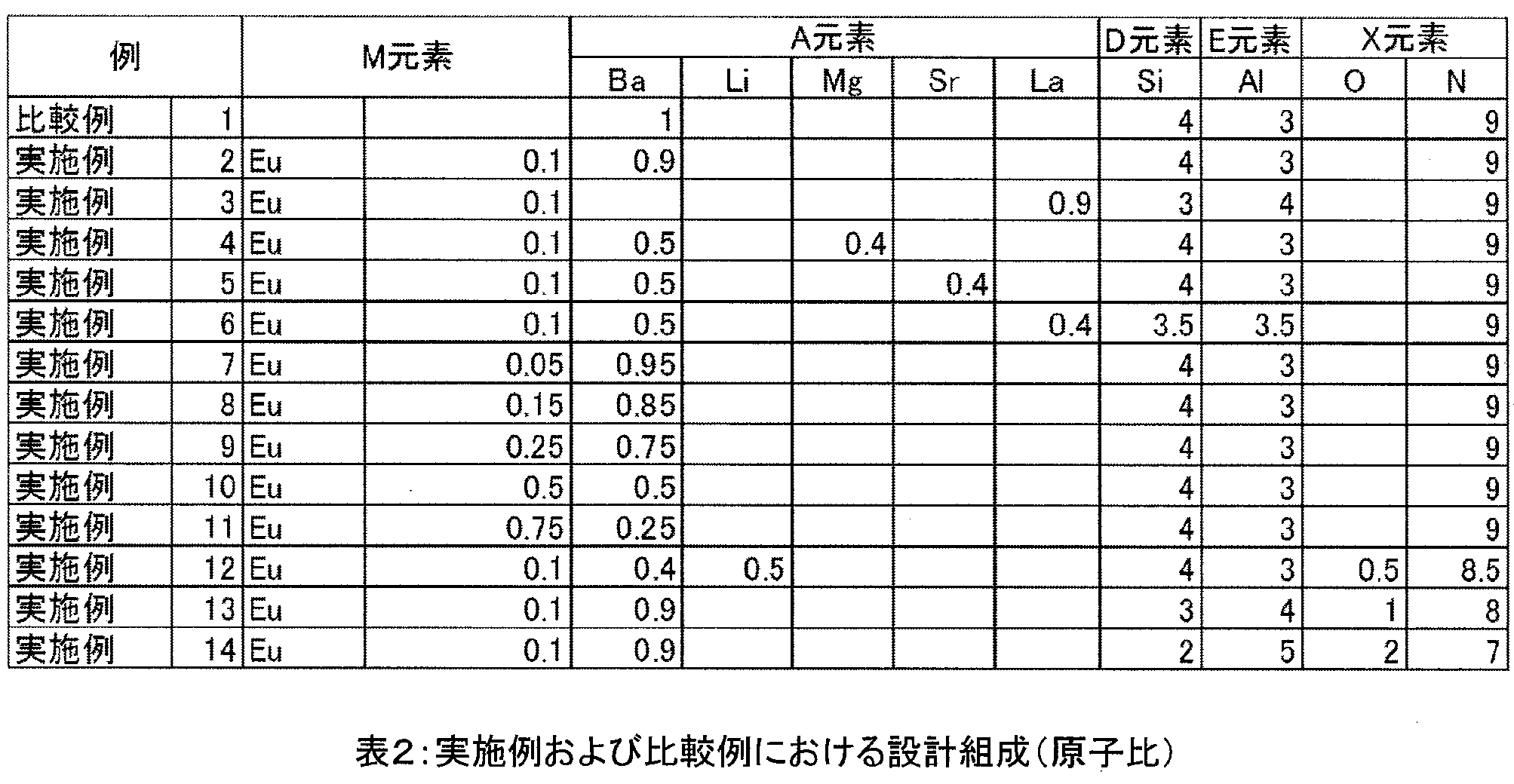
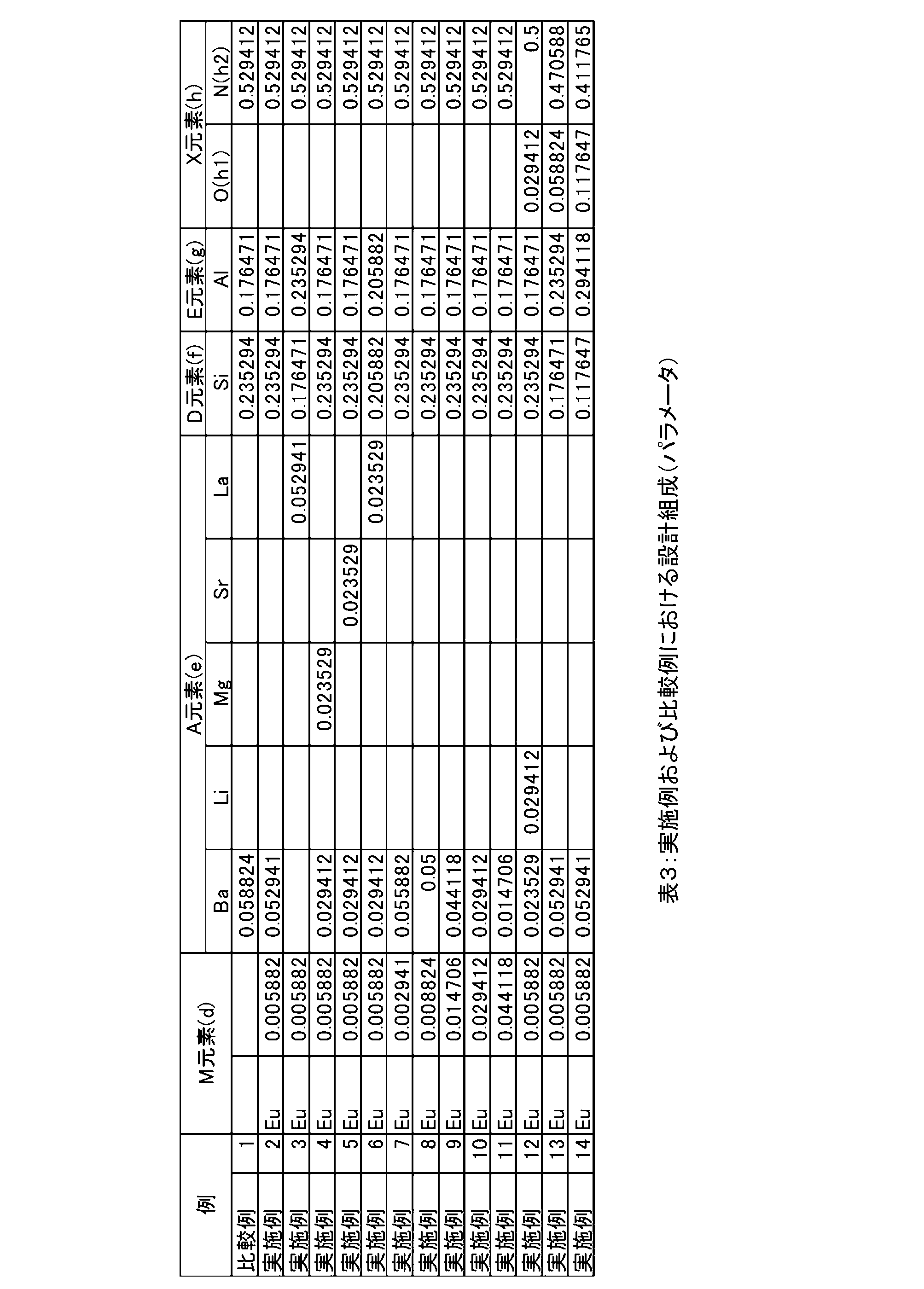
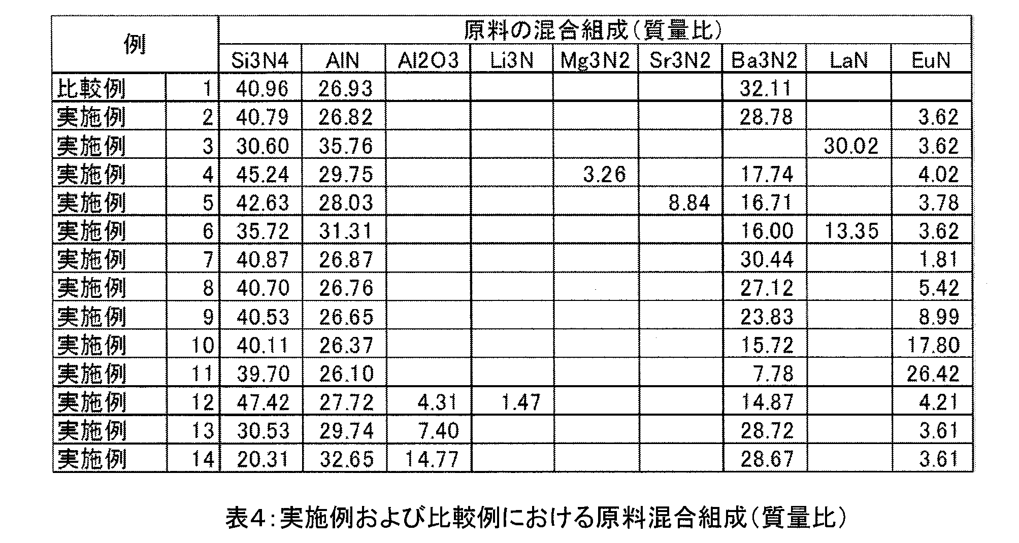
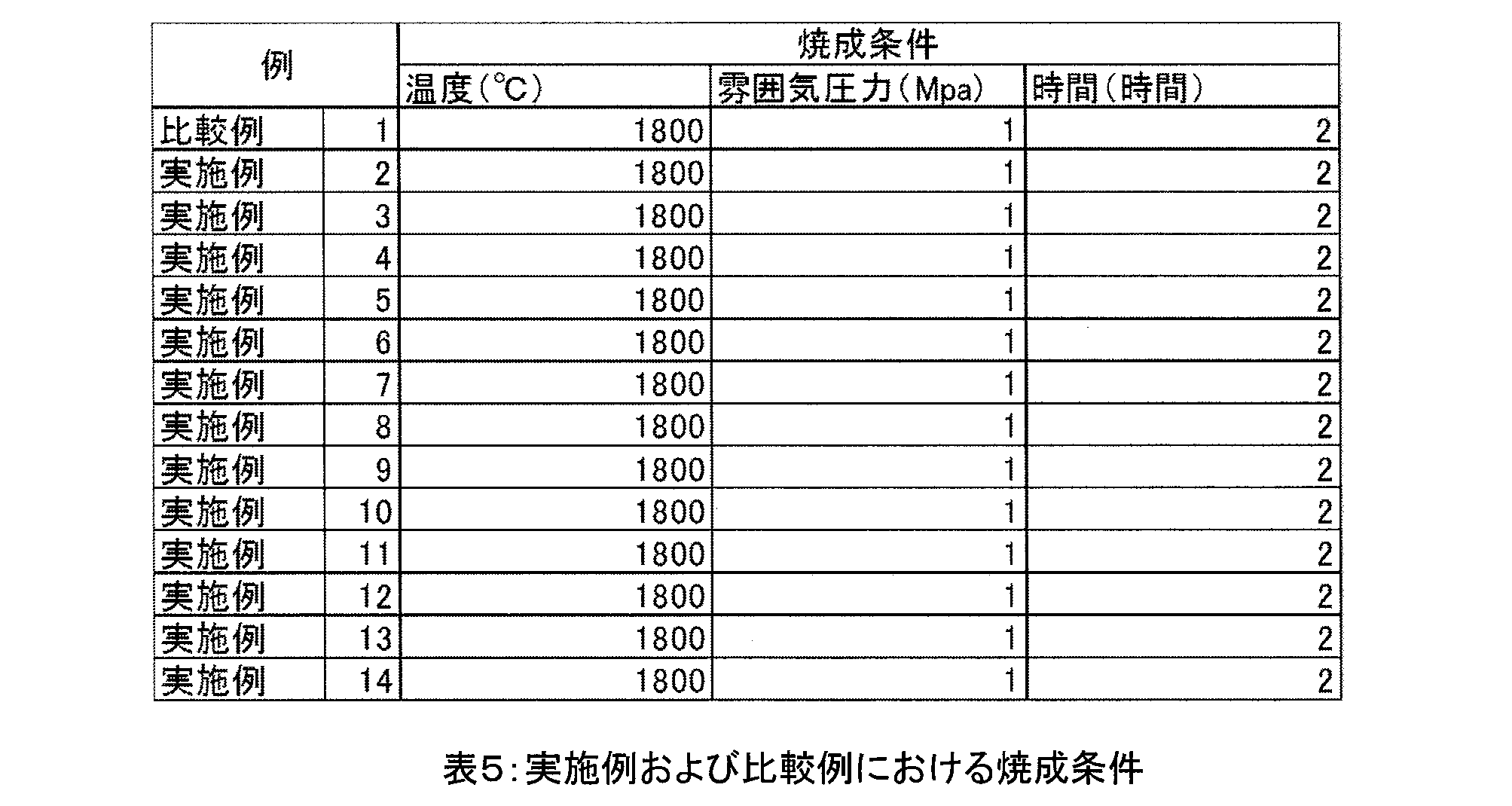
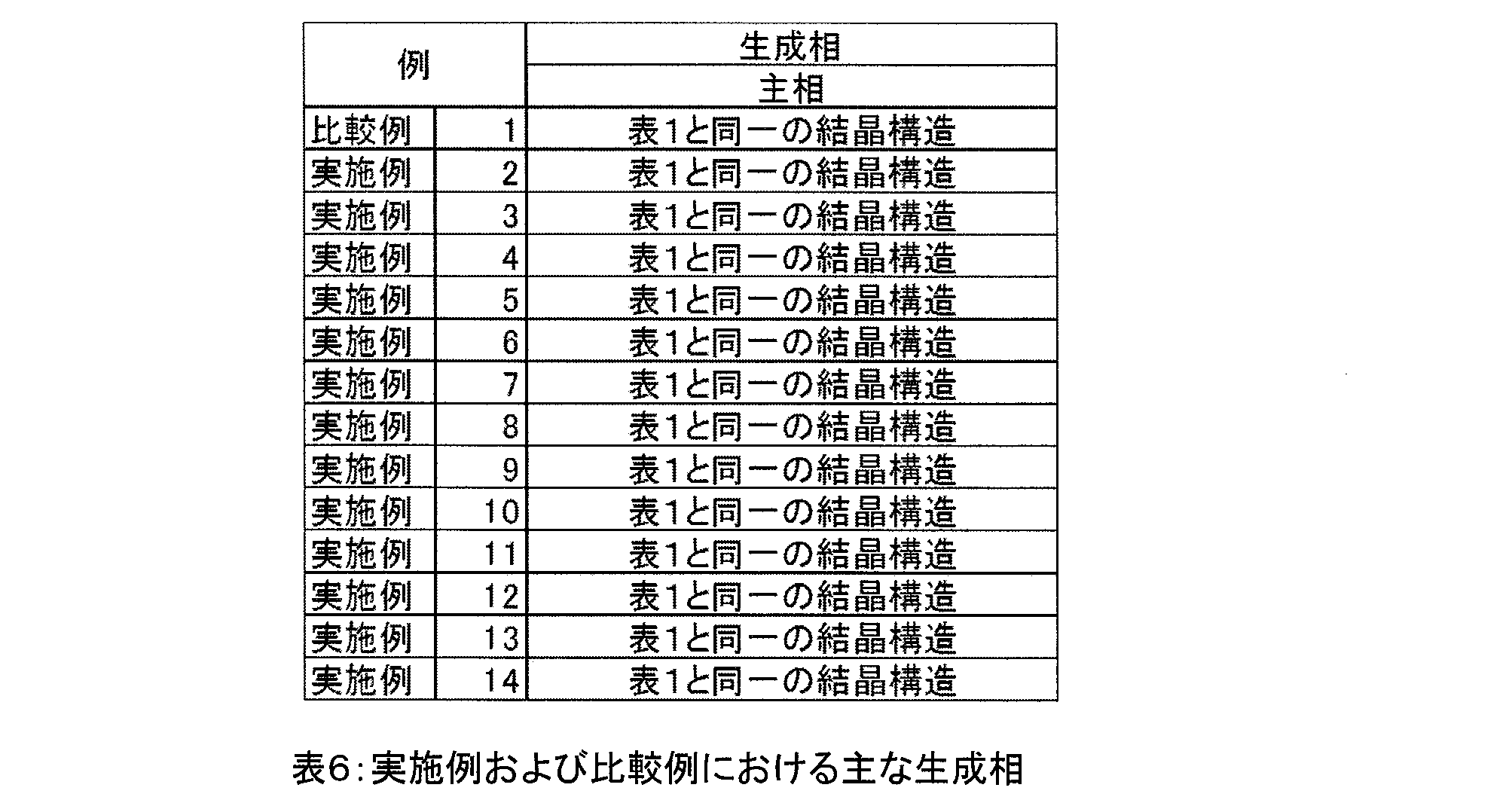
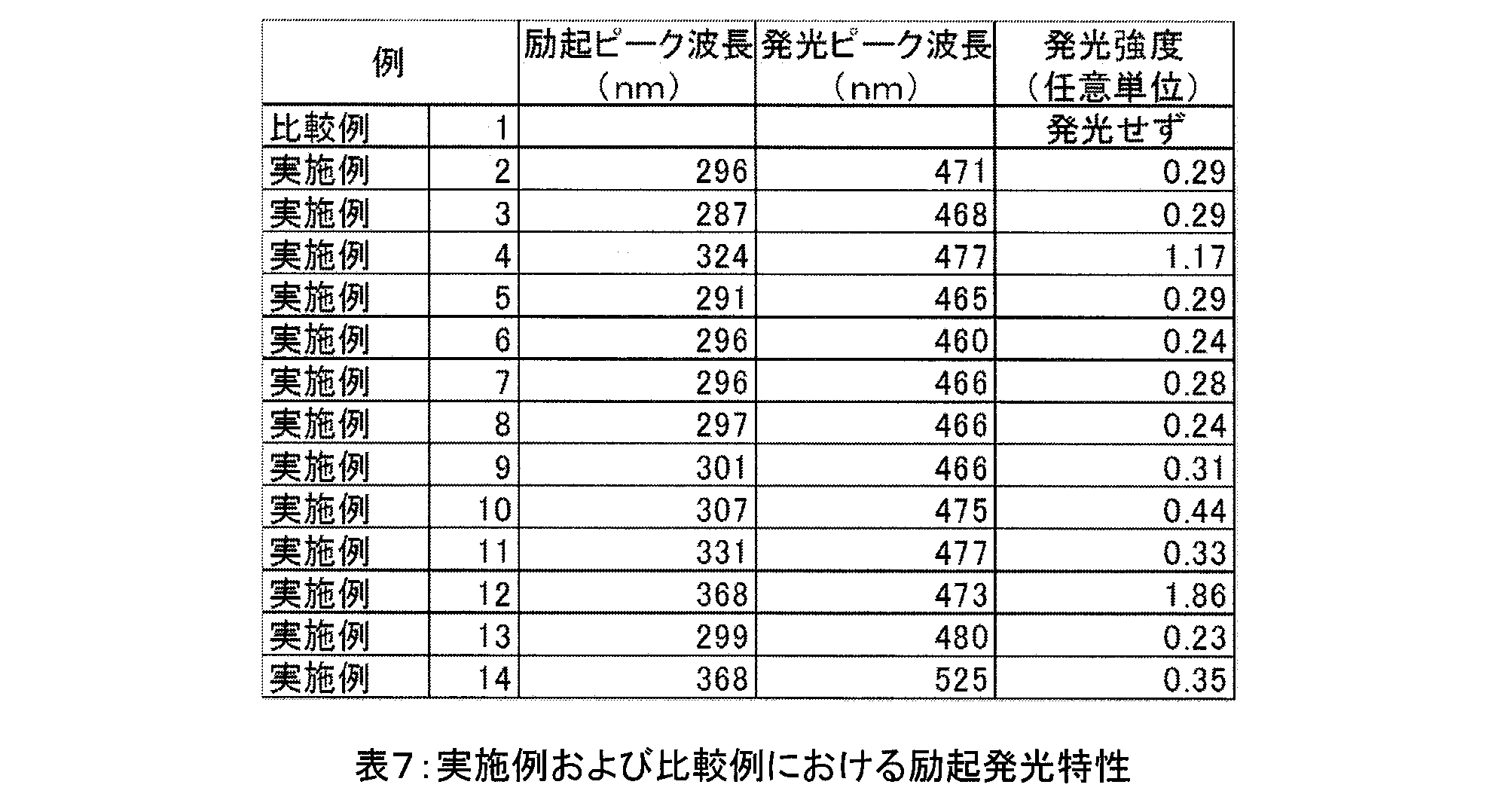
次に、本発明の蛍光体を用いた発光装置について説明する。
図5は、本発明による照明器具(砲弾型LED照明器具)を示す概略図である。
図6は、本発明による照明器具(基板実装型LED照明器具)を示す概略図である。
図7は、本発明による画像表示装置(プラズマディスプレイパネル)を示す概略図である。
図8は、本発明による画像表示装置(フィールドエミッションディスプレイパネル)を示す概略図である。
2、3.リードワイヤ。
4.発光ダイオード素子。
5.ボンディングワイヤ。
6、8.樹脂。
7.蛍光体。
11.基板実装用チップ型白色発光ダイオードランプ。
12、13.リードワイヤ。
14.発光ダイオード素子。
15.ボンディングワイヤ。
16、18.樹脂。
17.蛍光体。
19.アルミナセラミックス基板。
20.側面部材。
31.赤色蛍光体。
32.緑色蛍光体。
33.青色蛍光体。
34、35、36.紫外線発光セル。
37、38、39、40.電極。
41、42.誘電体層。
43.保護層。
44、45.ガラス基板。
51.ガラス。
52.陰極。
53.陽極。
54.ゲート。
55.エミッタ。
56.蛍光体。
57.電子。
Claims (57)
- 少なくともA元素とD元素とE元素とX元素(ただし、Aは、Li、Mg、Ca、Sr、Ba、Laから選ばれる1種または2種以上の元素、Dは、Si、Ge、Sn、Ti、Zr、Hfから選ばれる1種または2種以上の元素、Eは、B、Al、Ga、In、Sc、Yから選ばれる1種または2種以上の元素、Xは、O、N、Fから選ばれる1種または2種以上の元素)とを含む、Ba1Si4Al3N9で示される結晶、Ba1Si4Al3N9で示される結晶と同一の結晶構造を有する無機結晶、または、これらの固溶体結晶に、M元素(ただしMは、Mn、Ce、Pr、Nd、Sm、Eu、Tb、Dy、Ybから選ばれる1種または2種以上の元素)が固溶した無機化合物を含む、蛍光体。
- 前記Ba1Si4Al3N9で示される結晶と同一の結晶構造を有する無機結晶は、A1(D,E)7X9で示される結晶であり、少なくとも、A元素にLi、Mg、Ca、Sr、BaおよびLaからなる群から少なくとも1つ選択される元素を含み、D元素にSiを含み、E元素にAlを含み、X元素にNを含み、必要に応じてX元素にOを含む、請求項1に記載の蛍光体。
- 前記Ba1Si4Al3N9で示される結晶と同一の結晶構造を有する無機結晶は、Ba1Si4Al3N9、Mg1Si4Al3N9、Ca1Si4Al3N9、Sr1Si4Al3N9、La1Si4Al3N9、Li1Si4Al3N9、(Ba,Mg)1Si4Al3N9、(Ba,Ca)1Si4Al3N9、(Ba,Sr)1Si4Al3N9、(Ba,La)1Si4Al3N9、または、(Ba,Li)1Si4Al3N9である、請求項1に記載の蛍光体。
- 前記Ba1Si4Al3N9で示される結晶と同一の結晶構造を有する無機結晶は、
Ba1Si4-pAl3+pOpN9-p、Mg1Si4-pAl3+pOpN9-p、Ca1Si4-pAl3+pOpN9-p、Sr1Si4-pAl3+pOpN9-p、La1Si4-pAl3+pOpN9-p、Li1Si4-pAl3+pOpN9-p、(Ba,Mg)1Si4-pAl3+pOpN9-p、(Ba,Ca)1Si4-pAl3+pOpN9-p、(Ba,Sr)1Si4-pAl3+pOpN9-p、(Ba,La)1Si4-pAl3+pOpN9-p、または、(Ba,Li)1Si4-pAl3+pOpN9-p(ただし、0 ≦ p < 4)の組成式で示される、請求項1に記載の蛍光体。 - 前記M元素はEuである、請求項1に記載の蛍光体。
- 前記Ba1Si4Al3N9で示される結晶と同一の結晶構造を有する無機結晶は、単斜晶系の結晶である、請求項1に記載の蛍光体。
- 前記Ba1Si4Al3N9で示される結晶と同一の結晶構造を有する無機結晶は、単斜晶系の結晶であり、空間群P2(1)/cの対称性を持ち、
格子定数a、b、cは、
a = 0.58465±0.05 nm
b = 2.67255±0.05 nm
c = 0.58386±0.05 nm
の範囲の値である、請求項1に記載の蛍光体。 - 前記無機化合物は、組成式MdAeDfEgXh(ただし、式中d+e+f+g+h = 1であり、Mは、Mn、Ce、Pr、Nd、Sm、Eu、Tb、Dy、Ybから選ばれる1種または2種以上の元素、Aは、Li、Mg、Ca、Sr、Ba、Laから選ばれる1種または2種以上の元素、Dは、Si、Ge、Sn、Ti、Zr、Hfから選ばれる1種または2種以上の元素、Eは、B、Al、Ga、In、Sc、Yから選ばれる1種または2種以上の元素、Xは、O、N、Fから選ばれる1種または2種以上の元素)で示され、パラメータd、e、f、g、hは、
0.00001 ≦ d ≦ 0.05
0.01 ≦ e ≦ 0.07
0.10 ≦ f ≦ 0.30
0.10 ≦ g ≦ 0.30
0.45 ≦ h ≦ 0.65
の条件を全て満たす範囲の組成で表される、請求項1に記載の蛍光体。 - 前記パラメータd、e、f、g、hは、
d+e = (1/17)±0.05
f+g = (7/17)±0.05
h = (9/17)±0.05
の条件を全て満たす範囲の値である、請求項8に記載の蛍光体。 - 前記パラメータf、gは、
0/7 ≦ f/(f+g) ≦ 7/7
の条件を満たす、請求項8に記載の蛍光体。 - 前記X元素はOとNとを含み、前記無機化合物は、組成式MdAeDfEgOh1Nh2(ただし、式中d+e+f+g+h1+h2 = 1、および、h1+h2 = hである)で示され、
0/9 ≦ h1/(h1+h2) ≦ 6/9
の条件を満たす、請求項8に記載の蛍光体。 - 前記M元素として少なくともEuを含む、請求項8に記載の蛍光体。
- 前記A元素として少なくともBaを含み、前記D元素として少なくともSiを含み、前記E元素として少なくともAlを含み、前記X元素として少なくともNを含む、請求項8に記載の蛍光体。
- 前記無機化合物の組成式はパラメータpとqとを用いて
EuqBa1-qSi4-pAl3+pN9-pOp
ただし、
0 ≦ p < 4
0.0001 ≦ q < 1
で示される、請求項1に記載の蛍光体。 - 前記無機化合物は、平均粒径0.1μm以上20μm以下の単結晶粒子あるいは前記単結晶粒子の集合体である、請求項1に記載の蛍光体。
- 前記無機化合物に含まれる、Fe、Co、Ni不純物元素の合計が500ppm以下である、請求項1に記載の蛍光体。
- 前記無機化合物に加えて、前記無機化合物とは異なる他の結晶相あるいはアモルファス相をさらに含み、前記無機化合物の含有量は20質量%以上である、請求項1に記載の蛍光体。
- 前記他の結晶相あるいはアモルファス相は、導電性を持つ無機物質である、請求項17に記載の蛍光体。
- 前記導電性を持つ無機物質は、Zn、Al、Ga、In、Snから選ばれる1種または2種以上の元素を含む酸化物、酸窒化物、窒化物、あるいは、これらの混合物である、請求項18に記載の蛍光体。
- 前記他の結晶相あるいはアモルファス相は、前記蛍光体とは異なる無機蛍光体である、請求項17に記載の蛍光体。
- 励起源を照射することにより450nm以上530nm以下の範囲の波長にピークを持つ蛍光を発光する、請求項1に記載の蛍光体。
- 前記励起源は、100nm以上450nm未満の波長を持つ真空紫外線、紫外線または可視光、電子線またはX線である、請求項21に記載の蛍光体。
- 280nm以上405nm以下の光を照射すると450nm以上530nm以下の青色から緑色の蛍光を発する、請求項1に記載の蛍光体。
- 励起源が照射されたときに発光する色がCIE1931色度座標上の(x,y)の値で、
0 ≦ x ≦ 0.4
0 ≦ y ≦ 0.9
の条件を満たす、請求項1に記載の蛍光体。 - 金属化合物の混合物であって焼成することにより、請求項1に記載の無機化合物を構成しうる原料混合物を、窒素を含有する不活性雰囲気中において1200℃以上2200℃以下の温度範囲で焼成する、請求項1に記載の蛍光体の製造方法。
- 前記金属化合物の混合物は、Mを含有する化合物と、Aを含有する化合物と、Dを含有する化合物と、Eを含有する化合物と、Xを含有する化合物(ただし、Mは、Mn、Ce、Pr、Nd、Sm、Eu、Tb、Dy、Ybから選ばれる1種または2種以上の元素、Aは、Li、Mg、Ca、Sr、Ba、Laから選ばれる1種または2種以上の元素、Dは、Si、Ge、Sn、Ti、Zr、Hfから選ばれる1種または2種以上の元素、Eは、B、Al、Ga、In、Sc、Yから選ばれる1種または2種以上の元素、Xは、O、N、Fから選ばれる1種または2種以上の元素)とからなる、請求項25に記載の蛍光体の製造方法。
- 前記Mを含有する化合物は、Mを含有する金属、ケイ化物、酸化物、炭酸塩、窒化物、酸窒化物、塩化物、フッ化物、または酸フッ化物から選ばれる単体または2種以上の混合物であり、
前記Aを含有する化合物は、Aを含有する金属、ケイ化物、酸化物、炭酸塩、窒化物、酸窒化物、塩化物、フッ化物、または酸フッ化物から選ばれる単体または2種以上の混合物であり、
前記Dを含有する化合物は、Dを含有する金属、ケイ化物、酸化物、炭酸塩、窒化物、酸窒化物、塩化物、フッ化物、または酸フッ化物から選ばれる単体または2種以上の混合物であり、
前記Eを含有する化合物は、Eを含有する金属、ケイ化物、酸化物、炭酸塩、窒化物、酸窒化物、塩化物、フッ化物、または酸フッ化物から選ばれる単体または2種以上の混合物である、請求項26に記載の蛍光体の製造方法。 - 前記金属化合物の混合物は、少なくとも、ユーロピウムの窒化物または酸化物と、バリウムの窒化物、酸化物または炭酸塩と、酸化ケイ素または窒化ケイ素と、酸化アルミニウムまたは窒化アルミニウムとを含有する、請求項25に記載の蛍光体の製造方法。
- 前記窒素を含有する不活性雰囲気の圧力範囲は、0.1MPa以上100MPa以下であり、
前記窒素を含有する不活性雰囲気は窒素ガス雰囲気である、請求項25に記載の蛍光体の製造方法。 - 焼成炉の発熱体、断熱体、または試料容器に黒鉛を使用する、請求項25に記載の蛍光体の製造方法。
- 前記金属化合物の混合物の形状は、粉体または凝集体であり、
嵩密度40%以下の充填率に保持した状態で容器に充填した後に焼成する、請求項25に記載の蛍光体の製造方法。 - 前記金属化合物の混合物を窒化ホウ素製の容器に保持する、請求項25に記載の蛍光体の製造方法。
- 前記金属化合物の混合物の形状は、粉体または凝集体であり、
前記紛体または凝集体の平均粒径は、500μm以下である、請求項25に記載の蛍光体の製造方法。 - スプレイドライヤ、ふるい分け、または、風力分級を用いる、請求項33に記載の蛍光体の製造方法。
- 前記焼成は、常圧焼結法またはガス圧焼結法である、請求項25に記載の蛍光体の製造方法。
- 粉砕、分級、酸処理から選ばれる1種ないし複数の手法により、焼成により合成した蛍光体粉末の平均粒径を50nm以上20μm以下に粒度調整する、請求項25に記載の蛍光体の製造方法。
- 焼成後の蛍光体粉末、粉砕処理後の蛍光体粉末、または、粒度調整後の蛍光体粉末を、1000℃以上で焼成温度以下の温度で熱処理する、請求項25に記載の蛍光体の製造方法。
- 前記金属化合物の混合物に、焼成温度以下の温度で液相を生成する無機化合物を添加して焼成する、請求項25に記載の蛍光体の製造方法。
- 前記焼成温度以下の温度で液相を生成する無機化合物は、Li、Na、K、Mg、Ca、Sr、Baから選ばれる1種または2種以上の元素のフッ化物、塩化物、ヨウ化物、臭化物、あるいは、リン酸塩の1種または2種以上の混合物である、請求項38に記載の蛍光体の製造方法。
- 焼成後に溶剤で洗浄することにより、前記焼成温度以下の温度で液相を生成する無機化合物の含有量を低減させる、請求項38に記載の蛍光体の製造方法。
- 少なくとも発光体または発光光源と蛍光体とを備えた発光装置において、前記蛍光体は、少なくとも請求項1に記載の蛍光体を含む、発光装置。
- 前記発光体または発光光源は、280nm以上450nm未満の波長の光を発する発光ダイオード(LED)、レーザダイオード(LD)、半導体レーザ、または、有機EL発光体(OLED)である、請求項41に記載の発光装置。
- 前記発光装置は、白色発光ダイオード、複数の前記白色発光ダイオードを含む照明器具、または、液晶パネル用バックライトである、請求項41に記載の発光装置。
- 前記発光体または発光光源は、ピーク波長280nm以上450nm未満の紫外または可視光を発し、
請求項1に記載の蛍光体が発する青色から緑色と他の蛍光体が発する450nm以上の波長の光とを混合することにより白色光または白色光以外の光を発する、請求項41に記載の発光装置。 - 前記蛍光体は、前記発光体または発光光源によりピーク波長420nm以上500nm以下の光を発する青色蛍光体をさらに含む、請求項41に記載の発光装置。
- 前記青色蛍光体は、AlN:(Eu,Si)、BaMgAl10O17:Eu、SrSi9Al19ON31:Eu、LaSi9Al19N32:Eu、α-サイアロン:Ce、JEM:Ceから選ばれる、請求項45に記載の発光装置。
- 前記蛍光体は、前記発光体または発光光源によりピーク波長500nm以上550nm以下の光を発する緑色蛍光体をさらに含む、請求項41に記載の発光装置。
- 前記緑色蛍光体は、β-サイアロン:Eu、(Ba,Sr,Ca,Mg)2SiO4:Eu、(Ca,Sr,Ba)Si2O2N2:Euから選ばれる、請求項47に記載の発光装置。
- 前記蛍光体は、前記発光体または発光光源によりピーク波長550nm以上600nm以下の光を発する黄色蛍光体をさらに含む、請求項41に記載の発光装置。
- 前記黄色蛍光体は、YAG:Ce、α-サイアロン:Eu、CaAlSiN3:Ce、La3Si6N11:Ceから選ばれる、請求項49に記載の発光装置。
- 前記蛍光体は、前記発光体または発光光源によりピーク波長600nm以上700nm以下の光を発する赤色蛍光体をさらに含む、請求項41に記載の発光装置。
- 前記赤色蛍光体は、CaAlSiN3:Eu、(Ca,Sr)AlSiN3:Eu、Ca2Si5N8:Eu、Sr2Si5N8:Euから選ばれる、請求項51に記載の発光装置。
- 前記発光体または発光光源は、280nm以上450nm未満の波長の光を発するLEDである、請求項41に記載の発光装置。
- 少なくとも励起源および蛍光体を備えた画像表示装置において、前記蛍光体は、少なくとも請求項1に記載の蛍光体を含む、画像表示装置。
- 前記画像表示装置が、蛍光表示管(VFD)、フィールドエミッションディスプレイ(FED)、プラズマディスプレイパネル(PDP)、陰極線管(CRT)、または、液晶ディスプレイ(LCD)のいずれかである、請求項54に記載の画像表示装置。
- 請求項1に記載の無機化合物からなる顔料。
- 請求項1に記載の無機化合物からなる紫外線吸収剤。
Priority Applications (3)
| Application Number | Priority Date | Filing Date | Title |
|---|---|---|---|
| EP14797536.1A EP2998381B1 (en) | 2013-05-14 | 2014-05-13 | Phosphor, production method for same, light-emitting device, image display device, pigment, and ultraviolet absorber |
| JP2015517090A JP6083881B2 (ja) | 2013-05-14 | 2014-05-13 | 蛍光体、その製造方法、発光装置、画像表示装置、顔料および紫外線吸収剤 |
| US14/890,469 US9828547B2 (en) | 2013-05-14 | 2014-05-13 | Phosphor, production method for same, light-emitting device, image display device, pigment, and ultraviolet absorber |
Applications Claiming Priority (2)
| Application Number | Priority Date | Filing Date | Title |
|---|---|---|---|
| JP2013102141 | 2013-05-14 | ||
| JP2013-102141 | 2013-05-14 |
Publications (1)
| Publication Number | Publication Date |
|---|---|
| WO2014185415A1 true WO2014185415A1 (ja) | 2014-11-20 |
Family
ID=51898392
Family Applications (1)
| Application Number | Title | Priority Date | Filing Date |
|---|---|---|---|
| PCT/JP2014/062722 Ceased WO2014185415A1 (ja) | 2013-05-14 | 2014-05-13 | 蛍光体、その製造方法、発光装置、画像表示装置、顔料および紫外線吸収剤 |
Country Status (4)
| Country | Link |
|---|---|
| US (1) | US9828547B2 (ja) |
| EP (1) | EP2998381B1 (ja) |
| JP (1) | JP6083881B2 (ja) |
| WO (1) | WO2014185415A1 (ja) |
Cited By (10)
| Publication number | Priority date | Publication date | Assignee | Title |
|---|---|---|---|---|
| JP2015086360A (ja) * | 2013-09-25 | 2015-05-07 | 独立行政法人物質・材料研究機構 | 蛍光体及びその製造方法並びにこれを用いた発光装置 |
| CN107200589A (zh) * | 2016-03-18 | 2017-09-26 | 深圳市绎立锐光科技开发有限公司 | 一种氮化铝基质的荧光陶瓷的制备方法及相关荧光陶瓷 |
| JP2017179018A (ja) * | 2016-03-28 | 2017-10-05 | 国立研究開発法人物質・材料研究機構 | 蛍光体、その製造方法、発光装置、画像表示装置、顔料および紫外線吸収剤 |
| JP2017179020A (ja) * | 2016-03-28 | 2017-10-05 | 国立研究開発法人物質・材料研究機構 | 蛍光体、その製造方法、発光装置、画像表示装置、顔料および紫外線吸収剤 |
| WO2017170453A1 (ja) * | 2016-03-28 | 2017-10-05 | 国立研究開発法人物質・材料研究機構 | 蛍光体、その製造方法、発光装置、画像表示装置、顔料および紫外線吸収剤 |
| JP2017179021A (ja) * | 2016-03-28 | 2017-10-05 | 国立研究開発法人物質・材料研究機構 | 蛍光体、その製造方法、発光装置、画像表示装置、顔料および紫外線吸収剤 |
| JP2017179017A (ja) * | 2016-03-28 | 2017-10-05 | 国立研究開発法人物質・材料研究機構 | 蛍光体、その製造方法、発光装置、画像表示装置、顔料および紫外線吸収剤 |
| JP2017179019A (ja) * | 2016-03-28 | 2017-10-05 | 国立研究開発法人物質・材料研究機構 | 蛍光体、その製造方法、発光装置、画像表示装置、顔料および紫外線吸収剤 |
| KR20180107720A (ko) * | 2017-03-22 | 2018-10-02 | 그리렘 어드밴스드 머티리얼스 캄파니 리미티드 | 적외선 발광재료 및 이를 포함한 발광장치 |
| JPWO2022004406A1 (ja) * | 2020-07-03 | 2022-01-06 |
Families Citing this family (7)
| Publication number | Priority date | Publication date | Assignee | Title |
|---|---|---|---|---|
| KR102214065B1 (ko) * | 2014-02-20 | 2021-02-09 | 엘지전자 주식회사 | 산 질화물 형광체, 그 제조 방법 및 이를 이용한 발광 소자 패키지 |
| CN106197000A (zh) * | 2016-07-12 | 2016-12-07 | 广东工业大学 | 一种农作物太阳能空气能复合烘干机智能恒温控制系统 |
| DE102017108190A1 (de) * | 2017-04-18 | 2018-10-31 | Osram Opto Semiconductors Gmbh | Strahlungsemittierendes optoelektronisches Bauelement |
| JPWO2019164014A1 (ja) * | 2018-02-26 | 2021-02-04 | 京セラ株式会社 | 発光装置および照明装置 |
| DE102018004751B4 (de) * | 2018-06-13 | 2023-10-12 | OSRAM Opto Semiconductors Gesellschaft mit beschränkter Haftung | Leuchtstoff und beleuchtungsvorrichtung |
| CN109285937B (zh) | 2018-08-16 | 2020-03-20 | 佛山市国星光电股份有限公司 | Led白光器件及其制备方法、led背光模组 |
| WO2023123386A1 (zh) * | 2021-12-31 | 2023-07-06 | 苏州君诺新材科技有限公司 | 一种氮化物深红光材料及制备方法与器件 |
Citations (16)
| Publication number | Priority date | Publication date | Assignee | Title |
|---|---|---|---|---|
| JPH05152609A (ja) | 1991-11-25 | 1993-06-18 | Nichia Chem Ind Ltd | 発光ダイオード |
| JPH0799345A (ja) | 1993-09-28 | 1995-04-11 | Nichia Chem Ind Ltd | 発光ダイオード |
| JP2927279B2 (ja) | 1996-07-29 | 1999-07-28 | 日亜化学工業株式会社 | 発光ダイオード |
| WO2005019376A1 (ja) | 2003-08-22 | 2005-03-03 | National Institute For Materials Science | 酸窒化物蛍光体と発光器具 |
| JP2005112922A (ja) | 2003-10-03 | 2005-04-28 | National Institute For Materials Science | 酸窒化物蛍光体 |
| JP3668770B2 (ja) | 2001-06-07 | 2005-07-06 | 独立行政法人物質・材料研究機構 | 希土類元素を付活させた酸窒化物蛍光体 |
| WO2006033417A1 (ja) * | 2004-09-22 | 2006-03-30 | National Institute For Materials Science | 蛍光体とその製造方法および発光器具 |
| JP2006169526A (ja) * | 2004-12-10 | 2006-06-29 | Lumileds Lighting Us Llc | 燐光変換発光装置 |
| WO2006101096A1 (ja) | 2005-03-22 | 2006-09-28 | National Institute For Materials Science | 蛍光体とその製造方法および発光器具 |
| JP3837551B2 (ja) | 2003-06-20 | 2006-10-25 | 独立行政法人物質・材料研究機構 | 酸窒化物蛍光体 |
| JP3837588B2 (ja) | 2003-11-26 | 2006-10-25 | 独立行政法人物質・材料研究機構 | 蛍光体と蛍光体を用いた発光器具 |
| JP3921545B2 (ja) | 2004-03-12 | 2007-05-30 | 独立行政法人物質・材料研究機構 | 蛍光体とその製造方法 |
| WO2007066733A1 (ja) | 2005-12-08 | 2007-06-14 | National Institute For Materials Science | 蛍光体とその製造方法および発光器具 |
| JP2007326914A (ja) * | 2006-06-06 | 2007-12-20 | Sharp Corp | 酸窒化物蛍光体および発光装置 |
| JP2009167328A (ja) * | 2008-01-18 | 2009-07-30 | National Institute For Materials Science | 蛍光体とその製造方法および発光器具 |
| JP4524368B2 (ja) | 2004-04-22 | 2010-08-18 | 独立行政法人物質・材料研究機構 | サイアロン蛍光体とその製造方法 |
Family Cites Families (2)
| Publication number | Priority date | Publication date | Assignee | Title |
|---|---|---|---|---|
| DE10147040A1 (de) * | 2001-09-25 | 2003-04-24 | Patent Treuhand Ges Fuer Elektrische Gluehlampen Mbh | Beleuchtungseinheit mit mindestens einer LED als Lichtquelle |
| CN102348778B (zh) * | 2009-03-26 | 2014-09-10 | 独立行政法人物质·材料研究机构 | 荧光体、其制造方法、发光器具以及图像显示装置 |
-
2014
- 2014-05-13 JP JP2015517090A patent/JP6083881B2/ja active Active
- 2014-05-13 US US14/890,469 patent/US9828547B2/en not_active Expired - Fee Related
- 2014-05-13 EP EP14797536.1A patent/EP2998381B1/en not_active Not-in-force
- 2014-05-13 WO PCT/JP2014/062722 patent/WO2014185415A1/ja not_active Ceased
Patent Citations (16)
| Publication number | Priority date | Publication date | Assignee | Title |
|---|---|---|---|---|
| JPH05152609A (ja) | 1991-11-25 | 1993-06-18 | Nichia Chem Ind Ltd | 発光ダイオード |
| JPH0799345A (ja) | 1993-09-28 | 1995-04-11 | Nichia Chem Ind Ltd | 発光ダイオード |
| JP2927279B2 (ja) | 1996-07-29 | 1999-07-28 | 日亜化学工業株式会社 | 発光ダイオード |
| JP3668770B2 (ja) | 2001-06-07 | 2005-07-06 | 独立行政法人物質・材料研究機構 | 希土類元素を付活させた酸窒化物蛍光体 |
| JP3837551B2 (ja) | 2003-06-20 | 2006-10-25 | 独立行政法人物質・材料研究機構 | 酸窒化物蛍光体 |
| WO2005019376A1 (ja) | 2003-08-22 | 2005-03-03 | National Institute For Materials Science | 酸窒化物蛍光体と発光器具 |
| JP2005112922A (ja) | 2003-10-03 | 2005-04-28 | National Institute For Materials Science | 酸窒化物蛍光体 |
| JP3837588B2 (ja) | 2003-11-26 | 2006-10-25 | 独立行政法人物質・材料研究機構 | 蛍光体と蛍光体を用いた発光器具 |
| JP3921545B2 (ja) | 2004-03-12 | 2007-05-30 | 独立行政法人物質・材料研究機構 | 蛍光体とその製造方法 |
| JP4524368B2 (ja) | 2004-04-22 | 2010-08-18 | 独立行政法人物質・材料研究機構 | サイアロン蛍光体とその製造方法 |
| WO2006033417A1 (ja) * | 2004-09-22 | 2006-03-30 | National Institute For Materials Science | 蛍光体とその製造方法および発光器具 |
| JP2006169526A (ja) * | 2004-12-10 | 2006-06-29 | Lumileds Lighting Us Llc | 燐光変換発光装置 |
| WO2006101096A1 (ja) | 2005-03-22 | 2006-09-28 | National Institute For Materials Science | 蛍光体とその製造方法および発光器具 |
| WO2007066733A1 (ja) | 2005-12-08 | 2007-06-14 | National Institute For Materials Science | 蛍光体とその製造方法および発光器具 |
| JP2007326914A (ja) * | 2006-06-06 | 2007-12-20 | Sharp Corp | 酸窒化物蛍光体および発光装置 |
| JP2009167328A (ja) * | 2008-01-18 | 2009-07-30 | National Institute For Materials Science | 蛍光体とその製造方法および発光器具 |
Non-Patent Citations (2)
| Title |
|---|
| JOURNAL OF THE AMERICAN CERAMIC SOCIETY, vol. 85, no. 5, 2002, pages 1229 - 1234 |
| See also references of EP2998381A4 |
Cited By (16)
| Publication number | Priority date | Publication date | Assignee | Title |
|---|---|---|---|---|
| JP2015086360A (ja) * | 2013-09-25 | 2015-05-07 | 独立行政法人物質・材料研究機構 | 蛍光体及びその製造方法並びにこれを用いた発光装置 |
| CN107200589A (zh) * | 2016-03-18 | 2017-09-26 | 深圳市绎立锐光科技开发有限公司 | 一种氮化铝基质的荧光陶瓷的制备方法及相关荧光陶瓷 |
| CN107200589B (zh) * | 2016-03-18 | 2021-07-23 | 深圳光峰科技股份有限公司 | 一种氮化铝基质的荧光陶瓷的制备方法及相关荧光陶瓷 |
| US10968387B2 (en) * | 2016-03-28 | 2021-04-06 | National Institute For Materials Science | Phosphor, method for production same, light emitting device, image display, pigment and ultraviolet light absorber |
| JP2017179018A (ja) * | 2016-03-28 | 2017-10-05 | 国立研究開発法人物質・材料研究機構 | 蛍光体、その製造方法、発光装置、画像表示装置、顔料および紫外線吸収剤 |
| JP2017179020A (ja) * | 2016-03-28 | 2017-10-05 | 国立研究開発法人物質・材料研究機構 | 蛍光体、その製造方法、発光装置、画像表示装置、顔料および紫外線吸収剤 |
| WO2017170453A1 (ja) * | 2016-03-28 | 2017-10-05 | 国立研究開発法人物質・材料研究機構 | 蛍光体、その製造方法、発光装置、画像表示装置、顔料および紫外線吸収剤 |
| JP2017179021A (ja) * | 2016-03-28 | 2017-10-05 | 国立研究開発法人物質・材料研究機構 | 蛍光体、その製造方法、発光装置、画像表示装置、顔料および紫外線吸収剤 |
| JP2017179017A (ja) * | 2016-03-28 | 2017-10-05 | 国立研究開発法人物質・材料研究機構 | 蛍光体、その製造方法、発光装置、画像表示装置、顔料および紫外線吸収剤 |
| JP2017179019A (ja) * | 2016-03-28 | 2017-10-05 | 国立研究開発法人物質・材料研究機構 | 蛍光体、その製造方法、発光装置、画像表示装置、顔料および紫外線吸収剤 |
| KR20180107720A (ko) * | 2017-03-22 | 2018-10-02 | 그리렘 어드밴스드 머티리얼스 캄파니 리미티드 | 적외선 발광재료 및 이를 포함한 발광장치 |
| KR102093013B1 (ko) | 2017-03-22 | 2020-03-24 | 그리렘 어드밴스드 머티리얼스 캄파니 리미티드 | 적외선 발광재료 및 이를 포함한 발광장치 |
| JPWO2022004406A1 (ja) * | 2020-07-03 | 2022-01-06 | ||
| WO2022004406A1 (ja) * | 2020-07-03 | 2022-01-06 | デンカ株式会社 | 蛍光体、波長変換体、及び発光装置 |
| JP7453377B2 (ja) | 2020-07-03 | 2024-03-19 | デンカ株式会社 | 蛍光体、波長変換体、及び発光装置 |
| US12319859B2 (en) | 2020-07-03 | 2025-06-03 | Denka Company Limited | Phosphor, wavelength conversion body, and light emitting device |
Also Published As
| Publication number | Publication date |
|---|---|
| US9828547B2 (en) | 2017-11-28 |
| EP2998381A4 (en) | 2017-03-22 |
| JP6083881B2 (ja) | 2017-02-22 |
| EP2998381A1 (en) | 2016-03-23 |
| EP2998381B1 (en) | 2018-08-01 |
| US20160096991A1 (en) | 2016-04-07 |
| JPWO2014185415A1 (ja) | 2017-02-23 |
Similar Documents
| Publication | Publication Date | Title |
|---|---|---|
| JP6083881B2 (ja) | 蛍光体、その製造方法、発光装置、画像表示装置、顔料および紫外線吸収剤 | |
| JP5717075B2 (ja) | 蛍光体、その製造方法、発光装置および画像表示装置 | |
| JP5713305B2 (ja) | 蛍光体、その製造方法、発光装置および画像表示装置 | |
| JP5881092B2 (ja) | 蛍光体、その製造方法、発光装置および画像表示装置 | |
| JP5885175B2 (ja) | 蛍光体およびその製造方法、蛍光体を用いた発光装置、画像表示装置、顔料および紫外線吸収剤 | |
| JP6057213B2 (ja) | 蛍光体、その製造方法、発光装置および画像表示装置 | |
| JP6040500B2 (ja) | 蛍光体、その製造方法、発光装置および画像表示装置 | |
| JP6061331B2 (ja) | 蛍光体、その製造方法、発光装置および画像表示装置 | |
| JP6684412B1 (ja) | 蛍光体、その製造方法および発光装置 | |
| JP6176664B2 (ja) | 蛍光体、その製造方法、発光装置、画像表示装置、顔料、および、紫外線吸収剤 | |
| JP6074807B2 (ja) | 蛍光体、その製造方法、発光装置、画像表示装置、顔料、および、紫外線吸収剤 | |
| JP2017210529A (ja) | 蛍光体、その製造方法、発光装置、画像表示装置、顔料、および、紫外線吸収剤 | |
| JP5920773B2 (ja) | 蛍光体、その製造方法、発光装置および画像表示装置 | |
| JP2017179017A (ja) | 蛍光体、その製造方法、発光装置、画像表示装置、顔料および紫外線吸収剤 | |
| JP6700630B2 (ja) | 蛍光体、その製造方法、発光装置、画像表示装置、顔料および紫外線吸収剤 | |
| JP2017179020A (ja) | 蛍光体、その製造方法、発光装置、画像表示装置、顔料および紫外線吸収剤 | |
| JP2017179019A (ja) | 蛍光体、その製造方法、発光装置、画像表示装置、顔料および紫外線吸収剤 |
Legal Events
| Date | Code | Title | Description |
|---|---|---|---|
| 121 | Ep: the epo has been informed by wipo that ep was designated in this application |
Ref document number: 14797536 Country of ref document: EP Kind code of ref document: A1 |
|
| ENP | Entry into the national phase |
Ref document number: 2015517090 Country of ref document: JP Kind code of ref document: A |
|
| WWE | Wipo information: entry into national phase |
Ref document number: 14890469 Country of ref document: US |
|
| NENP | Non-entry into the national phase |
Ref country code: DE |
|
| WWE | Wipo information: entry into national phase |
Ref document number: 2014797536 Country of ref document: EP |