WO2014185589A1 - 유기 화합물, 유기 광전자 소자 및 표시 장치 - Google Patents
유기 화합물, 유기 광전자 소자 및 표시 장치 Download PDFInfo
- Publication number
- WO2014185589A1 WO2014185589A1 PCT/KR2013/007167 KR2013007167W WO2014185589A1 WO 2014185589 A1 WO2014185589 A1 WO 2014185589A1 KR 2013007167 W KR2013007167 W KR 2013007167W WO 2014185589 A1 WO2014185589 A1 WO 2014185589A1
- Authority
- WO
- WIPO (PCT)
- Prior art keywords
- group
- substituted
- unsubstituted
- organic
- layer
- Prior art date
- Legal status (The legal status is an assumption and is not a legal conclusion. Google has not performed a legal analysis and makes no representation as to the accuracy of the status listed.)
- Ceased
Links
Classifications
-
- H—ELECTRICITY
- H10—SEMICONDUCTOR DEVICES; ELECTRIC SOLID-STATE DEVICES NOT OTHERWISE PROVIDED FOR
- H10K—ORGANIC ELECTRIC SOLID-STATE DEVICES
- H10K85/00—Organic materials used in the body or electrodes of devices covered by this subclass
- H10K85/60—Organic compounds having low molecular weight
- H10K85/649—Aromatic compounds comprising a hetero atom
- H10K85/657—Polycyclic condensed heteroaromatic hydrocarbons
-
- C—CHEMISTRY; METALLURGY
- C07—ORGANIC CHEMISTRY
- C07D—HETEROCYCLIC COMPOUNDS
- C07D251/00—Heterocyclic compounds containing 1,3,5-triazine rings
- C07D251/02—Heterocyclic compounds containing 1,3,5-triazine rings not condensed with other rings
- C07D251/12—Heterocyclic compounds containing 1,3,5-triazine rings not condensed with other rings having three double bonds between ring members or between ring members and non-ring members
- C07D251/14—Heterocyclic compounds containing 1,3,5-triazine rings not condensed with other rings having three double bonds between ring members or between ring members and non-ring members with hydrogen or carbon atoms directly attached to at least one ring carbon atom
- C07D251/24—Heterocyclic compounds containing 1,3,5-triazine rings not condensed with other rings having three double bonds between ring members or between ring members and non-ring members with hydrogen or carbon atoms directly attached to at least one ring carbon atom to three ring carbon atoms
-
- C—CHEMISTRY; METALLURGY
- C07—ORGANIC CHEMISTRY
- C07D—HETEROCYCLIC COMPOUNDS
- C07D215/00—Heterocyclic compounds containing quinoline or hydrogenated quinoline ring systems
- C07D215/02—Heterocyclic compounds containing quinoline or hydrogenated quinoline ring systems having no bond between the ring nitrogen atom and a non-ring member or having only hydrogen atoms or carbon atoms directly attached to the ring nitrogen atom
- C07D215/04—Heterocyclic compounds containing quinoline or hydrogenated quinoline ring systems having no bond between the ring nitrogen atom and a non-ring member or having only hydrogen atoms or carbon atoms directly attached to the ring nitrogen atom with only hydrogen atoms or radicals containing only hydrogen and carbon atoms, directly attached to the ring carbon atoms
- C07D215/06—Heterocyclic compounds containing quinoline or hydrogenated quinoline ring systems having no bond between the ring nitrogen atom and a non-ring member or having only hydrogen atoms or carbon atoms directly attached to the ring nitrogen atom with only hydrogen atoms or radicals containing only hydrogen and carbon atoms, directly attached to the ring carbon atoms having only hydrogen atoms, hydrocarbon or substituted hydrocarbon radicals, attached to the ring nitrogen atom
-
- C—CHEMISTRY; METALLURGY
- C07—ORGANIC CHEMISTRY
- C07D—HETEROCYCLIC COMPOUNDS
- C07D277/00—Heterocyclic compounds containing 1,3-thiazole or hydrogenated 1,3-thiazole rings
- C07D277/60—Heterocyclic compounds containing 1,3-thiazole or hydrogenated 1,3-thiazole rings condensed with carbocyclic rings or ring systems
- C07D277/62—Benzothiazoles
- C07D277/64—Benzothiazoles with only hydrocarbon or substituted hydrocarbon radicals attached in position 2
- C07D277/66—Benzothiazoles with only hydrocarbon or substituted hydrocarbon radicals attached in position 2 with aromatic rings or ring systems directly attached in position 2
-
- C—CHEMISTRY; METALLURGY
- C07—ORGANIC CHEMISTRY
- C07D—HETEROCYCLIC COMPOUNDS
- C07D471/00—Heterocyclic compounds containing nitrogen atoms as the only ring hetero atoms in the condensed system, at least one ring being a six-membered ring with one nitrogen atom, not provided for by groups C07D451/00 - C07D463/00
- C07D471/02—Heterocyclic compounds containing nitrogen atoms as the only ring hetero atoms in the condensed system, at least one ring being a six-membered ring with one nitrogen atom, not provided for by groups C07D451/00 - C07D463/00 in which the condensed system contains two hetero rings
- C07D471/04—Ortho-condensed systems
-
- C—CHEMISTRY; METALLURGY
- C09—DYES; PAINTS; POLISHES; NATURAL RESINS; ADHESIVES; COMPOSITIONS NOT OTHERWISE PROVIDED FOR; APPLICATIONS OF MATERIALS NOT OTHERWISE PROVIDED FOR
- C09K—MATERIALS FOR MISCELLANEOUS APPLICATIONS, NOT PROVIDED FOR ELSEWHERE
- C09K11/00—Luminescent materials, e.g. electroluminescent or chemiluminescent
- C09K11/06—Luminescent materials, e.g. electroluminescent or chemiluminescent containing organic luminescent materials
-
- H—ELECTRICITY
- H10—SEMICONDUCTOR DEVICES; ELECTRIC SOLID-STATE DEVICES NOT OTHERWISE PROVIDED FOR
- H10K—ORGANIC ELECTRIC SOLID-STATE DEVICES
- H10K50/00—Organic light-emitting devices
- H10K50/10—OLEDs or polymer light-emitting diodes [PLED]
- H10K50/11—OLEDs or polymer light-emitting diodes [PLED] characterised by the electroluminescent [EL] layers
- H10K50/12—OLEDs or polymer light-emitting diodes [PLED] characterised by the electroluminescent [EL] layers comprising dopants
-
- H—ELECTRICITY
- H10—SEMICONDUCTOR DEVICES; ELECTRIC SOLID-STATE DEVICES NOT OTHERWISE PROVIDED FOR
- H10K—ORGANIC ELECTRIC SOLID-STATE DEVICES
- H10K85/00—Organic materials used in the body or electrodes of devices covered by this subclass
- H10K85/60—Organic compounds having low molecular weight
- H10K85/615—Polycyclic condensed aromatic hydrocarbons, e.g. anthracene
- H10K85/622—Polycyclic condensed aromatic hydrocarbons, e.g. anthracene containing four rings, e.g. pyrene
-
- H—ELECTRICITY
- H10—SEMICONDUCTOR DEVICES; ELECTRIC SOLID-STATE DEVICES NOT OTHERWISE PROVIDED FOR
- H10K—ORGANIC ELECTRIC SOLID-STATE DEVICES
- H10K85/00—Organic materials used in the body or electrodes of devices covered by this subclass
- H10K85/60—Organic compounds having low molecular weight
- H10K85/631—Amine compounds having at least two aryl rest on at least one amine-nitrogen atom, e.g. triphenylamine
- H10K85/636—Amine compounds having at least two aryl rest on at least one amine-nitrogen atom, e.g. triphenylamine comprising heteroaromatic hydrocarbons as substituents on the nitrogen atom
-
- H—ELECTRICITY
- H10—SEMICONDUCTOR DEVICES; ELECTRIC SOLID-STATE DEVICES NOT OTHERWISE PROVIDED FOR
- H10K—ORGANIC ELECTRIC SOLID-STATE DEVICES
- H10K85/00—Organic materials used in the body or electrodes of devices covered by this subclass
- H10K85/60—Organic compounds having low molecular weight
- H10K85/649—Aromatic compounds comprising a hetero atom
- H10K85/654—Aromatic compounds comprising a hetero atom comprising only nitrogen as heteroatom
-
- H—ELECTRICITY
- H10—SEMICONDUCTOR DEVICES; ELECTRIC SOLID-STATE DEVICES NOT OTHERWISE PROVIDED FOR
- H10K—ORGANIC ELECTRIC SOLID-STATE DEVICES
- H10K85/00—Organic materials used in the body or electrodes of devices covered by this subclass
- H10K85/60—Organic compounds having low molecular weight
- H10K85/649—Aromatic compounds comprising a hetero atom
- H10K85/656—Aromatic compounds comprising a hetero atom comprising two or more different heteroatoms per ring
-
- H—ELECTRICITY
- H10—SEMICONDUCTOR DEVICES; ELECTRIC SOLID-STATE DEVICES NOT OTHERWISE PROVIDED FOR
- H10K—ORGANIC ELECTRIC SOLID-STATE DEVICES
- H10K85/00—Organic materials used in the body or electrodes of devices covered by this subclass
- H10K85/60—Organic compounds having low molecular weight
- H10K85/649—Aromatic compounds comprising a hetero atom
- H10K85/657—Polycyclic condensed heteroaromatic hydrocarbons
- H10K85/6572—Polycyclic condensed heteroaromatic hydrocarbons comprising only nitrogen in the heteroaromatic polycondensed ring system, e.g. phenanthroline or carbazole
-
- C—CHEMISTRY; METALLURGY
- C09—DYES; PAINTS; POLISHES; NATURAL RESINS; ADHESIVES; COMPOSITIONS NOT OTHERWISE PROVIDED FOR; APPLICATIONS OF MATERIALS NOT OTHERWISE PROVIDED FOR
- C09K—MATERIALS FOR MISCELLANEOUS APPLICATIONS, NOT PROVIDED FOR ELSEWHERE
- C09K2211/00—Chemical nature of organic luminescent or tenebrescent compounds
- C09K2211/10—Non-macromolecular compounds
- C09K2211/1003—Carbocyclic compounds
- C09K2211/1007—Non-condensed systems
-
- C—CHEMISTRY; METALLURGY
- C09—DYES; PAINTS; POLISHES; NATURAL RESINS; ADHESIVES; COMPOSITIONS NOT OTHERWISE PROVIDED FOR; APPLICATIONS OF MATERIALS NOT OTHERWISE PROVIDED FOR
- C09K—MATERIALS FOR MISCELLANEOUS APPLICATIONS, NOT PROVIDED FOR ELSEWHERE
- C09K2211/00—Chemical nature of organic luminescent or tenebrescent compounds
- C09K2211/10—Non-macromolecular compounds
- C09K2211/1003—Carbocyclic compounds
- C09K2211/1011—Condensed systems
-
- C—CHEMISTRY; METALLURGY
- C09—DYES; PAINTS; POLISHES; NATURAL RESINS; ADHESIVES; COMPOSITIONS NOT OTHERWISE PROVIDED FOR; APPLICATIONS OF MATERIALS NOT OTHERWISE PROVIDED FOR
- C09K—MATERIALS FOR MISCELLANEOUS APPLICATIONS, NOT PROVIDED FOR ELSEWHERE
- C09K2211/00—Chemical nature of organic luminescent or tenebrescent compounds
- C09K2211/10—Non-macromolecular compounds
- C09K2211/1018—Heterocyclic compounds
- C09K2211/1025—Heterocyclic compounds characterised by ligands
- C09K2211/1029—Heterocyclic compounds characterised by ligands containing one nitrogen atom as the heteroatom
- C09K2211/1033—Heterocyclic compounds characterised by ligands containing one nitrogen atom as the heteroatom with oxygen
-
- C—CHEMISTRY; METALLURGY
- C09—DYES; PAINTS; POLISHES; NATURAL RESINS; ADHESIVES; COMPOSITIONS NOT OTHERWISE PROVIDED FOR; APPLICATIONS OF MATERIALS NOT OTHERWISE PROVIDED FOR
- C09K—MATERIALS FOR MISCELLANEOUS APPLICATIONS, NOT PROVIDED FOR ELSEWHERE
- C09K2211/00—Chemical nature of organic luminescent or tenebrescent compounds
- C09K2211/10—Non-macromolecular compounds
- C09K2211/1018—Heterocyclic compounds
- C09K2211/1025—Heterocyclic compounds characterised by ligands
- C09K2211/1029—Heterocyclic compounds characterised by ligands containing one nitrogen atom as the heteroatom
- C09K2211/1037—Heterocyclic compounds characterised by ligands containing one nitrogen atom as the heteroatom with sulfur
-
- C—CHEMISTRY; METALLURGY
- C09—DYES; PAINTS; POLISHES; NATURAL RESINS; ADHESIVES; COMPOSITIONS NOT OTHERWISE PROVIDED FOR; APPLICATIONS OF MATERIALS NOT OTHERWISE PROVIDED FOR
- C09K—MATERIALS FOR MISCELLANEOUS APPLICATIONS, NOT PROVIDED FOR ELSEWHERE
- C09K2211/00—Chemical nature of organic luminescent or tenebrescent compounds
- C09K2211/10—Non-macromolecular compounds
- C09K2211/1018—Heterocyclic compounds
- C09K2211/1025—Heterocyclic compounds characterised by ligands
- C09K2211/1044—Heterocyclic compounds characterised by ligands containing two nitrogen atoms as heteroatoms
-
- C—CHEMISTRY; METALLURGY
- C09—DYES; PAINTS; POLISHES; NATURAL RESINS; ADHESIVES; COMPOSITIONS NOT OTHERWISE PROVIDED FOR; APPLICATIONS OF MATERIALS NOT OTHERWISE PROVIDED FOR
- C09K—MATERIALS FOR MISCELLANEOUS APPLICATIONS, NOT PROVIDED FOR ELSEWHERE
- C09K2211/00—Chemical nature of organic luminescent or tenebrescent compounds
- C09K2211/10—Non-macromolecular compounds
- C09K2211/1018—Heterocyclic compounds
- C09K2211/1025—Heterocyclic compounds characterised by ligands
- C09K2211/1059—Heterocyclic compounds characterised by ligands containing three nitrogen atoms as heteroatoms
-
- H—ELECTRICITY
- H10—SEMICONDUCTOR DEVICES; ELECTRIC SOLID-STATE DEVICES NOT OTHERWISE PROVIDED FOR
- H10K—ORGANIC ELECTRIC SOLID-STATE DEVICES
- H10K2101/00—Properties of the organic materials covered by group H10K85/00
- H10K2101/10—Triplet emission
-
- H—ELECTRICITY
- H10—SEMICONDUCTOR DEVICES; ELECTRIC SOLID-STATE DEVICES NOT OTHERWISE PROVIDED FOR
- H10K—ORGANIC ELECTRIC SOLID-STATE DEVICES
- H10K2102/00—Constructional details relating to the organic devices covered by this subclass
- H10K2102/10—Transparent electrodes, e.g. using graphene
- H10K2102/101—Transparent electrodes, e.g. using graphene comprising transparent conductive oxides [TCO]
- H10K2102/103—Transparent electrodes, e.g. using graphene comprising transparent conductive oxides [TCO] comprising indium oxides, e.g. ITO
-
- H—ELECTRICITY
- H10—SEMICONDUCTOR DEVICES; ELECTRIC SOLID-STATE DEVICES NOT OTHERWISE PROVIDED FOR
- H10K—ORGANIC ELECTRIC SOLID-STATE DEVICES
- H10K50/00—Organic light-emitting devices
- H10K50/10—OLEDs or polymer light-emitting diodes [PLED]
- H10K50/14—Carrier transporting layers
- H10K50/15—Hole transporting layers
-
- H—ELECTRICITY
- H10—SEMICONDUCTOR DEVICES; ELECTRIC SOLID-STATE DEVICES NOT OTHERWISE PROVIDED FOR
- H10K—ORGANIC ELECTRIC SOLID-STATE DEVICES
- H10K50/00—Organic light-emitting devices
- H10K50/10—OLEDs or polymer light-emitting diodes [PLED]
- H10K50/14—Carrier transporting layers
- H10K50/16—Electron transporting layers
-
- H—ELECTRICITY
- H10—SEMICONDUCTOR DEVICES; ELECTRIC SOLID-STATE DEVICES NOT OTHERWISE PROVIDED FOR
- H10K—ORGANIC ELECTRIC SOLID-STATE DEVICES
- H10K50/00—Organic light-emitting devices
- H10K50/10—OLEDs or polymer light-emitting diodes [PLED]
- H10K50/17—Carrier injection layers
-
- H—ELECTRICITY
- H10—SEMICONDUCTOR DEVICES; ELECTRIC SOLID-STATE DEVICES NOT OTHERWISE PROVIDED FOR
- H10K—ORGANIC ELECTRIC SOLID-STATE DEVICES
- H10K50/00—Organic light-emitting devices
- H10K50/10—OLEDs or polymer light-emitting diodes [PLED]
- H10K50/17—Carrier injection layers
- H10K50/171—Electron injection layers
-
- H—ELECTRICITY
- H10—SEMICONDUCTOR DEVICES; ELECTRIC SOLID-STATE DEVICES NOT OTHERWISE PROVIDED FOR
- H10K—ORGANIC ELECTRIC SOLID-STATE DEVICES
- H10K50/00—Organic light-emitting devices
- H10K50/10—OLEDs or polymer light-emitting diodes [PLED]
- H10K50/18—Carrier blocking layers
-
- H—ELECTRICITY
- H10—SEMICONDUCTOR DEVICES; ELECTRIC SOLID-STATE DEVICES NOT OTHERWISE PROVIDED FOR
- H10K—ORGANIC ELECTRIC SOLID-STATE DEVICES
- H10K85/00—Organic materials used in the body or electrodes of devices covered by this subclass
- H10K85/30—Coordination compounds
- H10K85/321—Metal complexes comprising a group IIIA element, e.g. Tris (8-hydroxyquinoline) gallium [Gaq3]
- H10K85/324—Metal complexes comprising a group IIIA element, e.g. Tris (8-hydroxyquinoline) gallium [Gaq3] comprising aluminium, e.g. Alq3
-
- H—ELECTRICITY
- H10—SEMICONDUCTOR DEVICES; ELECTRIC SOLID-STATE DEVICES NOT OTHERWISE PROVIDED FOR
- H10K—ORGANIC ELECTRIC SOLID-STATE DEVICES
- H10K85/00—Organic materials used in the body or electrodes of devices covered by this subclass
- H10K85/30—Coordination compounds
- H10K85/341—Transition metal complexes, e.g. Ru(II)polypyridine complexes
- H10K85/342—Transition metal complexes, e.g. Ru(II)polypyridine complexes comprising iridium
Definitions
- An organic compound an organic optoelectronic device, and a display device.
- Organic optoelectric diodes are devices that can switch electrical energy and light energy.
- Organic optoelectronic devices can be divided into two types according to the principle of operation. One is that the excitons formed by light energy are electrons and holes
- a photovoltaic device that generates energy, and the other is a light emitting device that generates light energy from electrical energy by supplying a voltage or current to the electrode.
- Examples of the organic optoelectronic device may be an organic photoelectric device, an organic light emitting device, an organic solar cell and an organic photo conductor drum.
- organic light emitting diodes OLEDs
- the organic light emitting device converts electrical energy into light by applying an electric current to the organic light emitting material, and has a structure in which an organic layer is inserted between an anode and a cathode.
- the organic layer may comprise a light emitting layer and optionally an auxiliary layer, wherein the auxiliary layer is for example
- It may include at least one layer selected from a hole injection layer, a hole transport layer, an electron blocking layer, an electron transport layer, an electron injection layer and a hole blocking layer to increase the efficiency and stability of the organic light emitting device.
- the performance of the organic light emitting device is greatly influenced by the characteristics of the organic layer, and in particular, is affected by the organic material included in the organic layer.
- the mobility of holes and electrons may be increased, and electrochemical stability may be There is a need for the development of organic materials that can be enhanced.
- One embodiment provides an organic compound capable of implementing an organic optoelectronic device having improved driving voltage and efficiency.
- Another embodiment provides an organic optoelectronic device including the organic compound.
- Another embodiment provides a display device including the organic optoelectronic device.
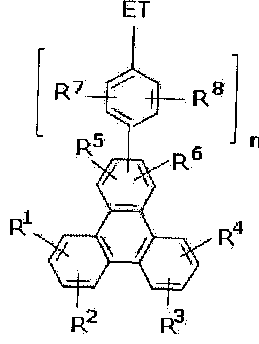
- an organic compound represented by Chemical Formula 1 is provided.
- ET is a functional group that can receive electrons when the electric field is applied
- R 1 to R 6 are each independently hydrogen, hydrogen, substituted or unsubstituted C1 to C30 alkyl group, substituted or unsubstituted C1 to C12 aryl group, or a combination thereof,
- R 7 and R 8 are each independently hydrogen, deuterium, a substituted or unsubstituted C1 to C10 alkyl group, or are connected to each other to form a fused ring, n is an integer of 0-3.
- an organic optoelectronic device comprising an anode and a cathode facing each other, at least one organic layer located between the anode and the cathode, the organic layer comprising the organic compound.
- a display device including the organic optoelectronic device is provided.
- FIG. 1 and 2 are cross-sectional views illustrating organic light emitting diodes according to example embodiments.
- substituted unless otherwise defined, at least one hydrogen of a substituent or a compound is a deuterium, a halogen group, a hydroxy group, an amino group, a substituted or unsubstituted C1 to C30 amine group, a nitro group, a substituted or unsubstituted C1 to C40 silyl group, C1 to C30 alkyl group, C1 to C10 alkylsilyl group, C3 to C30 cycloalkyl group, C3 to C30 heterocycloalkyl group, C6 to C30 aryl group, C6 to C30 heteroaryl group, C1 to C20 alkoxy group , Fluoro groups,
- substituted halogen group hydroxy group, amino group, substituted or unsubstituted C1 to C20 amine group, nitro group, substituted or unsubstituted C3 to C40 silyl group, C1 to C30 alkyl group, C1 to C10 alkylsilyl group, C3 to C30 cycloalkyl group, C3 to C30 heterocycloalkyl group, C6 to C30 aryl group, C6 to C30 heteroaryl group, C1 to C20 alkoxy group, fluoro group,
- Two adjacent adjacent substituents may be fused to form a ring.
- the substituted C6 to C30 aryl group can be fused to another adjacent substituted C6 to C30 aryl group to form a substituted or unsubstituted fluorene ring.
- hetero means one to three heteroatoms selected from the group consisting of N, 0, S, P and Si in one functional group, and the rest are carbon unless otherwise defined. do.
- alkyl (a lkyl) group means a separate definition, it means an aliphatic hydrocarbon group.
- the alkyl group may be a "saturated alkyl group” that does not contain any double or triple bonds.
- the alkyl group may be an alkyl group of C1 to C30. More specifically, the alkyl group may be a C1 to C20 alkyl group or a C1 to C10 alkyl group.
- a C1 to C4 alkyl group means that the alkyl chain contains 1 to 4 carbon atoms, and methyl, ethyl, propyl, iso-propyl, ⁇ -butyl, iso-butyl, sec -butyl and t-butyl Selected from the group consisting of:
- alkyl group examples include methyl group, ethyl group, propyl group, isopropyl group, butyl group, isobutyl group, t-butyl group, pentyl group, nucleosil group, cyclopropyl group, cyclobutyl group, cyclopentyl group and cyclonucleus It means a real pillar.
- an "aryl group” means a substituent in which all elements of a cyclic substituent have a p- orbital, and these P-orbitals form a conjugate, and are monocyclic, polycyclic or Fused ring polycyclic (ie, rings having adjacent pairs of carbon atoms) functional groups.
- heteroaryl group refers to N, 0, S, P and
- each ring may include 1 to 3 heteroatoms.
- a substituted or unsubstituted C6 to C30 aryl group and / or Substituted or unsubstituted C2 to C30 heteroaryl group is substituted or unsubstituted phenyl group, substituted or unsubstituted naphthyl group, substituted or unsubstituted anthracenyl group, substituted or unsubstituted phenanthryl group, substituted or unsubstituted Naphthacenyl group, substituted or unsubstituted pyrenyl group, substituted or unsubstituted biphenyl group, substituted or unsubstituted P-terphenyl group, substituted or unsubstituted m-terphenyl group, substituted or unsubstituted chrysenyl group, substituted Or an unsubstituted triphenylenyl group, a substituted or unsubstituted perenyl group, a substituted or
- the case of connecting to each other to form a fused ring means that naphthalene, triphenylene, anthracene, phenanthrene, tetralin, quinoline, indene, indane and the like are formed.
- the hole property refers to a property capable of forming holes by donating electrons when an electric field is applied. It has a conductive property along the level, which means that the holes formed in the anode facilitate the movement of the holes formed in the light emitting layer to the anode and the movement in the light emitting layer.
- the electron characteristic refers to a characteristic that can receive electrons when an electric field is applied, and has conductivity characteristics along the LUMO level, injecting electrons formed at the cathode into the light emitting layer, moving electrons formed in the light emitting layer to the cathode, and light emitting layer. It is a characteristic that facilitates the movement of from.
- An organic compound according to one embodiment is represented by Formula 1 below.
- ET is a functional group that can receive electrons when the electric field is applied
- R 1 to R 6 are each independently hydrogen, deuterium, a substituted or unsubstituted C1 to C30 alkyl group, a substituted or unsubstituted C1 to C12 aryl group, or a combination thereof,
- R 7 and R 8 are each independently hydrogen, deuterium, a substituted or unsubstituted C1 to C10 alkyl group, or are connected to each other to form a fused ring,
- n is an integer of 0-3.
- the organic compound may be represented by, for example, the following Formula 1-1 or 1- ⁇ depending on the bonding position of the triphenylene group. [Formula li]
- R 1 to R 8 , ET and n are as described above.
- the organic compound represented by Chemical Formula 1 includes a triphenylene group and a substituent having electronic properties.
- the organic compound may include a substituent having an electronic property, thereby making it easy to receive electrons when an electric field is applied, thereby lowering a driving voltage of the organic optoelectronic device to which the organic compound is applied.
- the organic compound includes a triphenylene moiety, which is easy to receive holes, and a moiety, which is easy to receive electrons, thereby forming a bipolar structure to properly balance the flow of holes and electrons, thereby applying the organic compound.
- the efficiency of the organic optoelectronic device can be improved.
- the organic compound properly localizes the triphenylene moiety and the electron susceptible moiety to reduce the flow of the conjugated system. By controlling, excellent bipolar characteristics can be exhibited. Accordingly, the lifespan of the organic optoelectronic device to which the organic compound is applied can be improved.
- the organic compound may have a structure capable of effectively preventing stacking of organic compounds, thereby lowering process stability and lowering deposition temperature.
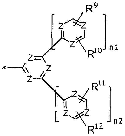
- the ET may comprise, for example, a heteroaryl group containing at least one nitrogen.
- the ET may be, for example, a functional group represented by Formula 2 below. [Formula 2]
- Z is independently N or CR a ,
- At least one of Z is N,
- R 9 to R 12 and R a are each independently hydrogen, hydrogen, substituted or unsubstituted C1 to C10 alkyl group, substituted or unsubstituted C6 to C12 aryl group, or a combination thereof,
- nl and n2 are each independently 0 or 1.
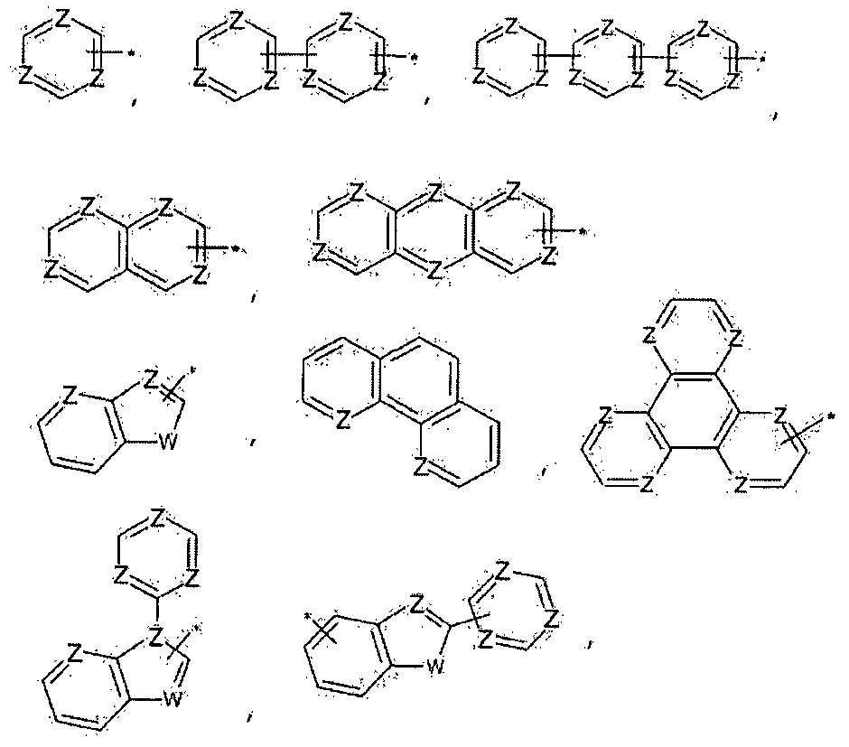
- the functional group represented by Formula 2 may be, for example, one of functional groups listed in Group 1 below.
- the ET can be, for example, substituted or unsubstituted functional groups listed in Group 2 below.
- W is each independently ⁇ , 0, S, SO, S0 2 , CR C , CR d R e , SiR f or
- R c to R ' are each independently hydrogen, hydrogen, substituted or unsubstituted C1 to C30 alkyl group, substituted or unsubstituted C3 to C30
- Cycloalkyl group substituted or unsubstituted C3 to C30 heterocycloalkyl group, substituted or unsubstituted C6 to C30 aryl group, substituted or unsubstituted C3 to C30 heteroaryl group, substituted or unsubstituted amine group, substituted or unsubstituted C6 to C30 arylamine group, substituted or unsubstituted C6 to C30 heteroarylamine group, substituted or unsubstituted C1 to C30 alkoxy group, substituted or unsubstituted C2 to C30 alkoxycarbonyl group, substituted or unsubstituted C2 to C30
- Aryloxycarbonylamino group substituted or unsubstituted C1 to C30
- connection point Is a connection point and may be located at any one of the elements forming the functional group.
- Substituted or unsubstituted functional groups listed in Group 2 may be, for example, substituted or unsubstituted functional groups listed in Group 3 below.
- the organic compound may be, for example, a compound listed in Group 4, but is not limited thereto.
- the organic compound may have a LUMO energy of about -2.0 to -2.5 eV. By having LUMO energy of the said range, an electron injection characteristic can be improved.
- organic optoelectronic device to which the aforementioned organic compound is applied will be described.
- the organic optoelectronic device is not particularly limited as long as the device can switch electrical energy and light energy, and examples thereof include organic photoelectric devices, organic light emitting devices, organic solar cells, and organic photosensitive drums.
- FIG. 1 and 2 are cross-sectional views illustrating an organic light emitting diode according to an embodiment.
- an organic optoelectronic device 100 includes an anode 120 and a cathode 110 facing each other, and an organic layer 105 positioned between the anode 120 and the cathode 110. Include.
- the anode 120 may be made of a high work function conductor, for example, to facilitate hole injection, and may be made of metal, metal oxide, and / or conductive polymer, for example.
- the anode 120 is, for example, a metal such as nickel, platinum, vanadium, chromium, copper, zinc, gold or an alloy thereof; Metal oxides such as zinc oxide, indium oxide, indium tin oxide (ITO), indium zinc oxide (IZO); ZnO and A1 Or a combination of a metal and an oxide, such as Sn0 2 and Sb; Conductive polymers such as poly (3-methylthiophene), poly (3,4- (ethylene-1,2-dioxy) thiophene Xpolyehtylenedioxythiophene (PEDT), polypyrrole and polyaniline, and the like. It doesn't happen.
- the cathode 110 has a low work function, for example, to facilitate electron injection.
- Cathode 110 is, for example, a metal such as magnesium, calcium, sodium, potassium, titanium, indium, yttrium, lithium, gadolinium, aluminum, silver, tin, lead, cesium, barium, or an alloy thereof; Multilayer structure materials such as LiF / Al, LiCVAl, LiF / Ca, LiF / Al, and BaFVCa, but are not limited thereto.
- the organic layer 105 is a light emitting layer 130 containing the above-described organic compound
- the light emitting layer 130 may include, for example, the above-described organic compound alone, or may include at least two kinds of the above-described organic compounds in combination, or may include a mixture of the organic compound and other compounds.
- the above-mentioned organic compound is mixed with other compound moles, for example,
- the host can be for example a phosphorescent host or a fluorescent host, for example a phosphorescent host.
- the dopant may be an inorganic, organic, or inorganic compound, and may be selected from known dopants.
- the organic light emitting diode 200 further includes a hole auxiliary layer 140 in addition to the light emitting layer 130.
- the hole auxiliary layer 140 may further increase hole injection and / or hole mobility between the anode 120 and the light emitting layer 130 and block electrons.
- the hole auxiliary layer 140 may be, for example, a hole transport layer, a hole injection layer, and / or an electron blocking layer, and may include at least one layer.
- the organic compound described above may be included in the emission layer 130 and / or the hole auxiliary layer 140.
- FIG. 1 In addition, in one embodiment of the present invention in FIG. 1
- an auxiliary electron transport layer, an electron transport layer, an electron injection layer may further include an auxiliary hole transport layer and a hole injection layer.
- the aforementioned organic compound may be included in the auxiliary electron transport layer, the electron transport layer, the electron injection layer, the auxiliary hole transport layer and / or the hole injection layer included in or additionally included in the emission layer 130 and / or the hole auxiliary layer 140. .
- the organic light emitting diodes 100 and 200 may be formed by forming a cathode or an anode on a substrate, followed by a dry film method such as evaporation, sputtering, plasma plating, and ion plating; Or after forming an organic layer by a wet film method such as spin coating, slit coating, dipping, flow coating, and inkjet printing, and the like, and thereon It can be prepared by forming a cathode or an anode.
- a dry film method such as evaporation, sputtering, plasma plating, and ion plating
- a wet film method such as spin coating, slit coating, dipping, flow coating, and inkjet printing, and the like, and thereon It can be prepared by forming a cathode or an anode.
- the organic light emitting diode described above may be applied to an organic light emitting diode display. [Form for implementation of invention]
- Compound 1-7 (38.6 g, 70%) was obtained by separation purification.
- Butylphosphine (0.66 g, 3.25 mmol) and sodium tert-butoxide (7.51 g, 78.1 mmol) were added sequentially and refluxed by heating at 10 (C for 16 hours. After completion of the reaction, water was added to the reaction solution and dichloromethane (DCM) was added. Extracted with After removing moisture with MgS04, it was filtered and concentrated under reduced pressure. The obtained residue was separated and purified through flash column chromatography, obtaining a compound 2 (20.9 g, 93%).
- An organic light emitting device was manufactured using Compound 1 obtained in Synthesis Example 8 as a host and Ir (PPy) 3 as a dopant.
- the anode is a ⁇ glass substrate having a sheet resistance value of 15 Q / cm 2 50 mm x 50 mm x 0.7 mm was cut into ultrasonic waves in acetone, isopropyl alcohol and pure water for 15 minutes, followed by UV ozone cleaning for 30 minutes.
- the amount of the phosphorescent dopyeon agent was deposited such that the weight 7 0/0, when the total amount of the light-emitting layer to increase 100%.
- Bis (2-methyl-8-quinolinolate) -4- (phenylphenolato) aluminum (BAlq) was deposited on the light emitting layer using the same vacuum deposition conditions to form a hole blocking layer having a thickness of 50 A.
- Alq 3 was deposited under the same vacuum deposition conditions to form an electron transport layer having a thickness of 200 A. remind
- LiF and A1 were sequentially deposited as a cathode on the electron transport layer.
- the structure of the organic photoelectric device is ITO / NPB (80 nm) / EML (Compound 1 (93% by weight) + Ir (PPy) 3 (7 increase 0 /.), 30 nm) / Balq (5 nm) / Alq3 ( 20 nm) / LiF (1 nm) / Al (100 nm).
- An organic light-emitting device was manufactured in the same manner as in Example 1, except that Compound 2 obtained in Synthesis Example 9 was used instead of Compound 1 obtained in Synthesis Example 8.
- An organic light emitting diode was manufactured according to the same method as Example 1 except for using Compound 3 obtained in Synthesis Example 10 instead of Compound 1 obtained in Synthesis Example 8.
- An organic light emitting diode was manufactured according to the same method as Example 1 except for using Compound 5 obtained in Synthesis Example 12 instead of Compound 1 obtained in Synthesis Example 8.
- An organic light emitting diode was manufactured according to the same method as Example 1 except for using CBP instead of Compound 1 obtained in Synthesis Example 8.
- the structure of the CBP is described below.
- NPB, BAlq, CBP and Ir (PPy) 3 used in the organic light emitting device is as follows.
- the current efficiency (cd / A) of the same current density (10 mA / cm 2) was calculated using the luminance, current density, and voltage measured from (1) and (2).
- the compound used in the light emitting layer of the organic light emitting device according to Examples 1 to 5 smoothly flows electrons and holes in the device by appropriate balance between a triphenylene which can receive holes well and a substituent that can accept electrons well. It seems to be due to one thing. Accordingly, it can be seen that the organic light emitting diodes according to Examples 1 to 5 can emit light at a lower driving voltage than the organic light emitting diode according to Comparative Example 1 and the luminous efficiency is also improved.
Landscapes
- Chemical & Material Sciences (AREA)
- Organic Chemistry (AREA)
- Engineering & Computer Science (AREA)
- Materials Engineering (AREA)
- Physics & Mathematics (AREA)
- Spectroscopy & Molecular Physics (AREA)
- Optics & Photonics (AREA)
- Electroluminescent Light Sources (AREA)
- Nitrogen Condensed Heterocyclic Rings (AREA)
Abstract
Description


Claims


Priority Applications (4)
| Application Number | Priority Date | Filing Date | Title |
|---|---|---|---|
| EP13884517.7A EP2998300A4 (en) | 2013-05-16 | 2013-08-08 | Organic compound, organic optoelectronic element, and display device |
| JP2016513849A JP2016526029A (ja) | 2013-05-16 | 2013-08-08 | 有機化合物、有機光電子素子および表示装置 |
| CN201380076662.0A CN105209442A (zh) | 2013-05-16 | 2013-08-08 | 有机化合物、有机光电子元件及显示器件 |
| US14/767,725 US20150364694A1 (en) | 2013-05-16 | 2013-08-08 | Organic compound, organic optoelectronic element, and display device |
Applications Claiming Priority (2)
| Application Number | Priority Date | Filing Date | Title |
|---|---|---|---|
| KR10-2013-0055955 | 2013-05-16 | ||
| KR20130055955A KR20140135532A (ko) | 2013-05-16 | 2013-05-16 | 유기 화합물, 유기 광전자 소자 및 표시 장치 |
Publications (1)
| Publication Number | Publication Date |
|---|---|
| WO2014185589A1 true WO2014185589A1 (ko) | 2014-11-20 |
Family
ID=51898550
Family Applications (1)
| Application Number | Title | Priority Date | Filing Date |
|---|---|---|---|
| PCT/KR2013/007167 Ceased WO2014185589A1 (ko) | 2013-05-16 | 2013-08-08 | 유기 화합물, 유기 광전자 소자 및 표시 장치 |
Country Status (6)
| Country | Link |
|---|---|
| US (1) | US20150364694A1 (ko) |
| EP (1) | EP2998300A4 (ko) |
| JP (1) | JP2016526029A (ko) |
| KR (1) | KR20140135532A (ko) |
| CN (1) | CN105209442A (ko) |
| WO (1) | WO2014185589A1 (ko) |
Cited By (5)
| Publication number | Priority date | Publication date | Assignee | Title |
|---|---|---|---|---|
| US20160181524A1 (en) * | 2014-12-19 | 2016-06-23 | Samsung Display Co., Ltd. | Organic light-emitting device |
| US20160322583A1 (en) * | 2013-12-27 | 2016-11-03 | Doosan Corporation | Organic electroluminescent device |
| CN107001292A (zh) * | 2015-04-24 | 2017-08-01 | 三星Sdi株式会社 | 有机光电元件用化合物及有机光电元件及显示元件 |
| US10230053B2 (en) | 2015-01-30 | 2019-03-12 | Samsung Display Co., Ltd. | Organic light-emitting device |
| US10305041B2 (en) | 2014-11-10 | 2019-05-28 | Samsung Display Co., Ltd. | Organic light-emitting device |
Families Citing this family (12)
| Publication number | Priority date | Publication date | Assignee | Title |
|---|---|---|---|---|
| USRE47654E1 (en) | 2010-01-15 | 2019-10-22 | Idemitsu Koasn Co., Ltd. | Organic electroluminescence device |
| KR101600453B1 (ko) * | 2013-09-13 | 2016-03-08 | 주식회사 엠비케이 | 신규한 유기발광화합물 및 이를 포함하는 유기전기발광소자 |
| KR102385230B1 (ko) | 2014-11-19 | 2022-04-12 | 삼성디스플레이 주식회사 | 유기 발광 소자 |
| KR102633649B1 (ko) * | 2015-11-19 | 2024-04-17 | 솔루스첨단소재 주식회사 | 유기 화합물 및 이를 포함하는 유기 전계 발광 소자 |
| KR102617840B1 (ko) * | 2015-11-26 | 2023-12-26 | 덕산네오룩스 주식회사 | 유기전기소자용 화합물, 이를 이용한 유기전기소자 및 그 전자 장치 |
| CN108822096B (zh) * | 2018-04-27 | 2020-09-25 | 陕西莱特光电材料股份有限公司 | 一种新型主体发光材料及其合成方法与应用 |
| CN108530437B (zh) * | 2018-04-27 | 2020-12-04 | 陕西莱特光电材料股份有限公司 | 一种主体发光材料及其合成方法与应用 |
| KR102745953B1 (ko) * | 2019-06-27 | 2024-12-23 | 솔루스첨단소재 주식회사 | 유기 전계 발광 소자 |
| US12545667B2 (en) * | 2019-11-19 | 2026-02-10 | Duk San Neolux Co., Ltd. | Compound for organic electronic element, organic electronic element using the same, and an electronic device thereof |
| US11849635B2 (en) * | 2020-02-28 | 2023-12-19 | Samsung Display Co., Ltd. | Organic electroluminescence device and compound for organic electroluminescence device |
| JP2023156118A (ja) * | 2022-04-12 | 2023-10-24 | キヤノン株式会社 | 有機化合物及び有機発光素子 |
| CN114853749A (zh) * | 2022-05-10 | 2022-08-05 | 长春海谱润斯科技股份有限公司 | 一种杂环化合物及包含该杂环化合物的有机电致发光器件 |
Citations (3)
| Publication number | Priority date | Publication date | Assignee | Title |
|---|---|---|---|---|
| KR20110123172A (ko) * | 2010-05-06 | 2011-11-14 | 주식회사 두산 | 방향족 아민을 포함하는 트리페닐렌계 화합물 및 이를 포함하는 유기 전계 발광 소자 |
| WO2012048781A1 (de) * | 2010-10-15 | 2012-04-19 | Merck Patent Gmbh | Materialien auf basis von triphenylen für organische elektrolumineszenzvorrichtungen |
| KR20120131870A (ko) * | 2011-05-26 | 2012-12-05 | 제일모직주식회사 | 유기광전자소자용 화합물, 이를 포함하는 유기발광소자 및 상기 유기발광소자를 포함하는 표시장치 |
Family Cites Families (20)
| Publication number | Priority date | Publication date | Assignee | Title |
|---|---|---|---|---|
| US3711567A (en) * | 1970-12-16 | 1973-01-16 | American Cyanamid Co | Bis-triphenylenes and use in photochromic and luminescent compositions |
| JP4646494B2 (ja) * | 2002-04-11 | 2011-03-09 | 出光興産株式会社 | 新規含窒素複素環誘導体及びそれを用いた有機エレクトロルミネッセンス素子 |
| CN101146814B (zh) * | 2005-03-01 | 2013-01-02 | 新加坡科技研究局 | 经溶液加工的有机金属配合物及其在电致发光器件中的用途 |
| JP5896600B2 (ja) * | 2007-04-04 | 2016-03-30 | ビーエーエスエフ ソシエタス・ヨーロピアBasf Se | 赤から緑までのスペクトル領域において発光する新規の有機金属錯体およびそのoledにおける使用 |
| TW200910661A (en) * | 2007-04-04 | 2009-03-01 | Koninkl Philips Electronics Nv | OLED with metal complexes having a high quantum efficiency |
| TWI501943B (zh) * | 2007-08-08 | 2015-10-01 | Universal Display Corp | 磷光發光二極體內之單聯伸三苯發色團 |
| KR20090111915A (ko) * | 2008-04-23 | 2009-10-28 | (주)그라쎌 | 신규한 유기 발광 화합물 및 이를 발광재료로서 채용하고있는 유기 발광 소자 |
| JP2010138121A (ja) * | 2008-12-12 | 2010-06-24 | Canon Inc | トリアジン化合物及びこれを用いた有機発光素子 |
| KR101724304B1 (ko) * | 2009-10-16 | 2017-04-10 | 에스에프씨 주식회사 | 축합방향족 화합물 및 이를 포함하는 유기전계발광소자 |
| KR20110043240A (ko) * | 2009-10-21 | 2011-04-27 | 에스케이 텔레콤주식회사 | 근거리 영역 내에서의 데이터 전송 시스템 및 방법, 그리고 이에 적용되는 장치 |
| KR20110043270A (ko) * | 2009-10-21 | 2011-04-27 | (주)씨에스엘쏠라 | 유기발광화합물 및 이를 구비한 유기발광소자 |
| USRE47654E1 (en) * | 2010-01-15 | 2019-10-22 | Idemitsu Koasn Co., Ltd. | Organic electroluminescence device |
| KR101794557B1 (ko) * | 2010-04-16 | 2017-11-08 | 에스에프씨 주식회사 | 아민계 화합물 및 이를 포함하는 유기전계발광소자 |
| US8968887B2 (en) * | 2010-04-28 | 2015-03-03 | Universal Display Corporation | Triphenylene-benzofuran/benzothiophene/benzoselenophene compounds with substituents joining to form fused rings |
| KR101244599B1 (ko) * | 2010-05-28 | 2013-03-25 | 주식회사 두산 | 바이폴라 트리페닐렌계 화합물 및 이를 포함하는 유기 전계 발광 소자 |
| JP5778407B2 (ja) * | 2010-07-29 | 2015-09-16 | ユー・ディー・シー アイルランド リミテッド | 有機電界発光素子及び電荷輸送材料 |
| US8413633B2 (en) * | 2010-08-05 | 2013-04-09 | Hyundai Motor Company | Rollerized cranktrain bedplate, reciprocating engine embodying same and engine further including rollerized cranktrain |
| CN102532105A (zh) * | 2010-12-17 | 2012-07-04 | 清华大学 | 一种含有吡啶基团的三亚苯类化合物及其应用 |
| JP5839912B2 (ja) * | 2011-09-22 | 2016-01-06 | 株式会社半導体エネルギー研究所 | 発光素子、発光装置 |
| KR20140135525A (ko) * | 2013-05-16 | 2014-11-26 | 제일모직주식회사 | 유기 광전자 소자용 발광 재료, 유기 광전자 소자 및 표시 장치 |
-
2013
- 2013-05-16 KR KR20130055955A patent/KR20140135532A/ko not_active Ceased
- 2013-08-08 US US14/767,725 patent/US20150364694A1/en not_active Abandoned
- 2013-08-08 EP EP13884517.7A patent/EP2998300A4/en not_active Withdrawn
- 2013-08-08 CN CN201380076662.0A patent/CN105209442A/zh active Pending
- 2013-08-08 JP JP2016513849A patent/JP2016526029A/ja active Pending
- 2013-08-08 WO PCT/KR2013/007167 patent/WO2014185589A1/ko not_active Ceased
Patent Citations (3)
| Publication number | Priority date | Publication date | Assignee | Title |
|---|---|---|---|---|
| KR20110123172A (ko) * | 2010-05-06 | 2011-11-14 | 주식회사 두산 | 방향족 아민을 포함하는 트리페닐렌계 화합물 및 이를 포함하는 유기 전계 발광 소자 |
| WO2012048781A1 (de) * | 2010-10-15 | 2012-04-19 | Merck Patent Gmbh | Materialien auf basis von triphenylen für organische elektrolumineszenzvorrichtungen |
| KR20120131870A (ko) * | 2011-05-26 | 2012-12-05 | 제일모직주식회사 | 유기광전자소자용 화합물, 이를 포함하는 유기발광소자 및 상기 유기발광소자를 포함하는 표시장치 |
Non-Patent Citations (2)
| Title |
|---|
| PARK, J. ET AL.: "Thermally stable triphenylene-based hole-transporting materials for organic ligbt-emitting devices", THIN SOLID FILMS, vol. 519, 31 March 2011 (2011-03-31), pages 5917 - 5923, XP028227159 * |
| See also references of EP2998300A4 * |
Cited By (13)
| Publication number | Priority date | Publication date | Assignee | Title |
|---|---|---|---|---|
| US20160322583A1 (en) * | 2013-12-27 | 2016-11-03 | Doosan Corporation | Organic electroluminescent device |
| JP2019145818A (ja) * | 2013-12-27 | 2019-08-29 | ドゥーサン コーポレイション | 有機電界発光素子 |
| US10573822B2 (en) * | 2013-12-27 | 2020-02-25 | Doosan Corporation | Organic electroluminescent device |
| US12441935B2 (en) | 2013-12-27 | 2025-10-14 | Solus Advanced Materials Co., Ltd. | Organic electroluminescent device |
| US11588109B2 (en) | 2013-12-27 | 2023-02-21 | Solus Advanced Materials Co., Ltd. | Organic electroluminescent device |
| US10305041B2 (en) | 2014-11-10 | 2019-05-28 | Samsung Display Co., Ltd. | Organic light-emitting device |
| US10978643B2 (en) * | 2014-12-19 | 2021-04-13 | Samsung Display Co., Ltd. | Organic light-emitting device |
| CN105720203A (zh) * | 2014-12-19 | 2016-06-29 | 三星显示有限公司 | 有机发光器件 |
| US20160181524A1 (en) * | 2014-12-19 | 2016-06-23 | Samsung Display Co., Ltd. | Organic light-emitting device |
| US10230053B2 (en) | 2015-01-30 | 2019-03-12 | Samsung Display Co., Ltd. | Organic light-emitting device |
| CN107001292A (zh) * | 2015-04-24 | 2017-08-01 | 三星Sdi株式会社 | 有机光电元件用化合物及有机光电元件及显示元件 |
| US10797245B2 (en) | 2015-04-24 | 2020-10-06 | Samsung Sdi Co., Ltd. | Compound for organic optoelectronic element, organic optoelectronic element, and display device |
| CN107001292B (zh) * | 2015-04-24 | 2020-05-19 | 三星Sdi株式会社 | 有机光电元件用化合物及有机光电元件及显示元件 |
Also Published As
| Publication number | Publication date |
|---|---|
| CN105209442A (zh) | 2015-12-30 |
| JP2016526029A (ja) | 2016-09-01 |
| KR20140135532A (ko) | 2014-11-26 |
| US20150364694A1 (en) | 2015-12-17 |
| EP2998300A4 (en) | 2017-05-17 |
| EP2998300A1 (en) | 2016-03-23 |
Similar Documents
| Publication | Publication Date | Title |
|---|---|---|
| JP6257113B2 (ja) | 有機化合物、有機光電子素子および表示装置 | |
| JP6431530B2 (ja) | 有機光電子素子用発光材料、有機光電子素子および表示装置 | |
| JP6335288B2 (ja) | 有機化合物、有機光電子素子および表示装置 | |
| WO2014185589A1 (ko) | 유기 화합물, 유기 광전자 소자 및 표시 장치 | |
| EP2952511B1 (en) | Organic compound, organic optoelectronic device and display device | |
| KR101653338B1 (ko) | 유기 화합물, 유기 광전자 소자 및 표시 장치 | |
| US20160329506A1 (en) | Organic compound, organic optoelectronic device, and display device | |
| WO2014104515A1 (ko) | 유기광전자소자용 화합물, 이를 포함하는 유기발광소자 및 상기 유기발광소자를 포함하는 표시장치 | |
| TW201710245A (zh) | 有機化合物及有機光電裝置和顯示裝置 | |
| WO2017099326A1 (ko) | 유기 광전자 소자용 화합물, 유기 광전자 소자 및 표시 장치 | |
| KR101702512B1 (ko) | 유기 화합물, 유기 광전자 소자 및 표시 장치 | |
| CN112592333B (zh) | 用于有机光电装置的化合物、有机光电装置及显示装置 | |
| WO2015005536A1 (ko) | 화합물, 이를 포함하는 유기 광전자 소자 및 표시장치 | |
| WO2014104600A1 (ko) | 유기광전자소자용 화합물, 이를 포함하는 유기발광소자 및 상기 유기발광소자를 포함하는 표시장치 | |
| KR101693613B1 (ko) | 화합물, 이를 포함하는 유기 광전자 소자 및 표시장치 | |
| KR101733651B1 (ko) | 화합물, 이를 포함하는 유기 광전자 소자 및 표시장치 | |
| KR20150024669A (ko) | 화합물, 이를 포함하는 유기발광소자 및 상기 유기발광소자를 포함하는 표시장치 | |
| KR101653337B1 (ko) | 화합물, 이를 포함하는 유기 광전자 소자 및 상기 유기 광전자 소자를 포함하는 표시장치 |
Legal Events
| Date | Code | Title | Description |
|---|---|---|---|
| 121 | Ep: the epo has been informed by wipo that ep was designated in this application |
Ref document number: 13884517 Country of ref document: EP Kind code of ref document: A1 |
|
| WWE | Wipo information: entry into national phase |
Ref document number: 14767725 Country of ref document: US |
|
| ENP | Entry into the national phase |
Ref document number: 2016513849 Country of ref document: JP Kind code of ref document: A |
|
| NENP | Non-entry into the national phase |
Ref country code: DE |
|
| WWE | Wipo information: entry into national phase |
Ref document number: 2013884517 Country of ref document: EP |