WO2014188760A1 - Module - Google Patents
Module Download PDFInfo
- Publication number
- WO2014188760A1 WO2014188760A1 PCT/JP2014/056192 JP2014056192W WO2014188760A1 WO 2014188760 A1 WO2014188760 A1 WO 2014188760A1 JP 2014056192 W JP2014056192 W JP 2014056192W WO 2014188760 A1 WO2014188760 A1 WO 2014188760A1
- Authority
- WO
- WIPO (PCT)
- Prior art keywords
- columnar conductor
- resin layer
- sealing resin
- substrate
- substrate electrode
- Prior art date
- Legal status (The legal status is an assumption and is not a legal conclusion. Google has not performed a legal analysis and makes no representation as to the accuracy of the status listed.)
- Ceased
Links
Images


Classifications
-
- H—ELECTRICITY
- H05—ELECTRIC TECHNIQUES NOT OTHERWISE PROVIDED FOR
- H05K—PRINTED CIRCUITS; CASINGS OR CONSTRUCTIONAL DETAILS OF ELECTRIC APPARATUS; MANUFACTURE OF ASSEMBLAGES OF ELECTRICAL COMPONENTS
- H05K1/00—Printed circuits
- H05K1/02—Details
- H05K1/11—Printed elements for providing electric connections to or between printed circuits
- H05K1/111—Pads for surface mounting, e.g. lay-out
-
- H—ELECTRICITY
- H05—ELECTRIC TECHNIQUES NOT OTHERWISE PROVIDED FOR
- H05K—PRINTED CIRCUITS; CASINGS OR CONSTRUCTIONAL DETAILS OF ELECTRIC APPARATUS; MANUFACTURE OF ASSEMBLAGES OF ELECTRICAL COMPONENTS
- H05K1/00—Printed circuits
- H05K1/02—Details
- H05K1/11—Printed elements for providing electric connections to or between printed circuits
- H05K1/115—Via connections; Lands around holes or via connections
-
- H—ELECTRICITY
- H05—ELECTRIC TECHNIQUES NOT OTHERWISE PROVIDED FOR
- H05K—PRINTED CIRCUITS; CASINGS OR CONSTRUCTIONAL DETAILS OF ELECTRIC APPARATUS; MANUFACTURE OF ASSEMBLAGES OF ELECTRICAL COMPONENTS
- H05K1/00—Printed circuits
- H05K1/18—Printed circuits structurally associated with non-printed electric components
- H05K1/181—Printed circuits structurally associated with non-printed electric components associated with surface mounted components
-
- H—ELECTRICITY
- H05—ELECTRIC TECHNIQUES NOT OTHERWISE PROVIDED FOR
- H05K—PRINTED CIRCUITS; CASINGS OR CONSTRUCTIONAL DETAILS OF ELECTRIC APPARATUS; MANUFACTURE OF ASSEMBLAGES OF ELECTRICAL COMPONENTS
- H05K3/00—Apparatus or processes for manufacturing printed circuits
- H05K3/22—Secondary treatment of printed circuits
- H05K3/28—Applying non-metallic protective coatings
- H05K3/284—Applying non-metallic protective coatings for encapsulating mounted components
-
- H—ELECTRICITY
- H05—ELECTRIC TECHNIQUES NOT OTHERWISE PROVIDED FOR
- H05K—PRINTED CIRCUITS; CASINGS OR CONSTRUCTIONAL DETAILS OF ELECTRIC APPARATUS; MANUFACTURE OF ASSEMBLAGES OF ELECTRICAL COMPONENTS
- H05K3/00—Apparatus or processes for manufacturing printed circuits
- H05K3/40—Forming printed elements for providing electric connections to or between printed circuits
- H05K3/4007—Surface contacts, e.g. bumps
-
- H—ELECTRICITY
- H10—SEMICONDUCTOR DEVICES; ELECTRIC SOLID-STATE DEVICES NOT OTHERWISE PROVIDED FOR
- H10W—GENERIC PACKAGES, INTERCONNECTIONS, CONNECTORS OR OTHER CONSTRUCTIONAL DETAILS OF DEVICES COVERED BY CLASS H10
- H10W70/00—Package substrates; Interposers; Redistribution layers [RDL]
- H10W70/60—Insulating or insulated package substrates; Interposers; Redistribution layers
- H10W70/62—Insulating or insulated package substrates; Interposers; Redistribution layers characterised by their interconnections
- H10W70/63—Vias, e.g. via plugs
- H10W70/635—Through-vias
-
- H—ELECTRICITY
- H10—SEMICONDUCTOR DEVICES; ELECTRIC SOLID-STATE DEVICES NOT OTHERWISE PROVIDED FOR
- H10W—GENERIC PACKAGES, INTERCONNECTIONS, CONNECTORS OR OTHER CONSTRUCTIONAL DETAILS OF DEVICES COVERED BY CLASS H10
- H10W74/00—Encapsulations, e.g. protective coatings
- H10W74/10—Encapsulations, e.g. protective coatings characterised by their shape or disposition
- H10W74/111—Encapsulations, e.g. protective coatings characterised by their shape or disposition the semiconductor body being completely enclosed
- H10W74/114—Encapsulations, e.g. protective coatings characterised by their shape or disposition the semiconductor body being completely enclosed by a substrate and the encapsulations
-
- H—ELECTRICITY
- H10—SEMICONDUCTOR DEVICES; ELECTRIC SOLID-STATE DEVICES NOT OTHERWISE PROVIDED FOR
- H10W—GENERIC PACKAGES, INTERCONNECTIONS, CONNECTORS OR OTHER CONSTRUCTIONAL DETAILS OF DEVICES COVERED BY CLASS H10
- H10W90/00—Package configurations
- H10W90/701—Package configurations characterised by the relative positions of pads or connectors relative to package parts
-
- H—ELECTRICITY
- H05—ELECTRIC TECHNIQUES NOT OTHERWISE PROVIDED FOR
- H05K—PRINTED CIRCUITS; CASINGS OR CONSTRUCTIONAL DETAILS OF ELECTRIC APPARATUS; MANUFACTURE OF ASSEMBLAGES OF ELECTRICAL COMPONENTS
- H05K2201/00—Indexing scheme relating to printed circuits covered by H05K1/00
- H05K2201/03—Conductive materials
- H05K2201/0332—Structure of the conductor
- H05K2201/0364—Conductor shape
- H05K2201/0367—Metallic bump or raised conductor not used as solder bump
-
- H—ELECTRICITY
- H05—ELECTRIC TECHNIQUES NOT OTHERWISE PROVIDED FOR
- H05K—PRINTED CIRCUITS; CASINGS OR CONSTRUCTIONAL DETAILS OF ELECTRIC APPARATUS; MANUFACTURE OF ASSEMBLAGES OF ELECTRICAL COMPONENTS
- H05K2201/00—Indexing scheme relating to printed circuits covered by H05K1/00
- H05K2201/06—Thermal details
- H05K2201/068—Thermal details wherein the coefficient of thermal expansion is important
-
- H—ELECTRICITY
- H05—ELECTRIC TECHNIQUES NOT OTHERWISE PROVIDED FOR
- H05K—PRINTED CIRCUITS; CASINGS OR CONSTRUCTIONAL DETAILS OF ELECTRIC APPARATUS; MANUFACTURE OF ASSEMBLAGES OF ELECTRICAL COMPONENTS
- H05K2203/00—Indexing scheme relating to apparatus or processes for manufacturing printed circuits covered by H05K3/00
- H05K2203/02—Details related to mechanical or acoustic processing, e.g. drilling, punching, cutting, using ultrasound
- H05K2203/025—Abrading, e.g. grinding or sand blasting
-
- H—ELECTRICITY
- H05—ELECTRIC TECHNIQUES NOT OTHERWISE PROVIDED FOR
- H05K—PRINTED CIRCUITS; CASINGS OR CONSTRUCTIONAL DETAILS OF ELECTRIC APPARATUS; MANUFACTURE OF ASSEMBLAGES OF ELECTRICAL COMPONENTS
- H05K2203/00—Indexing scheme relating to apparatus or processes for manufacturing printed circuits covered by H05K3/00
- H05K2203/05—Patterning and lithography; Masks; Details of resist
- H05K2203/0562—Details of resist
- H05K2203/0588—Second resist used as pattern over first resist
-
- H—ELECTRICITY
- H10—SEMICONDUCTOR DEVICES; ELECTRIC SOLID-STATE DEVICES NOT OTHERWISE PROVIDED FOR
- H10W—GENERIC PACKAGES, INTERCONNECTIONS, CONNECTORS OR OTHER CONSTRUCTIONAL DETAILS OF DEVICES COVERED BY CLASS H10
- H10W70/00—Package substrates; Interposers; Redistribution layers [RDL]
- H10W70/60—Insulating or insulated package substrates; Interposers; Redistribution layers
- H10W70/611—Insulating or insulated package substrates; Interposers; Redistribution layers for connecting multiple chips together
- H10W70/614—Insulating or insulated package substrates; Interposers; Redistribution layers for connecting multiple chips together the multiple chips being integrally enclosed
-
- H—ELECTRICITY
- H10—SEMICONDUCTOR DEVICES; ELECTRIC SOLID-STATE DEVICES NOT OTHERWISE PROVIDED FOR
- H10W—GENERIC PACKAGES, INTERCONNECTIONS, CONNECTORS OR OTHER CONSTRUCTIONAL DETAILS OF DEVICES COVERED BY CLASS H10
- H10W72/00—Interconnections or connectors in packages
- H10W72/071—Connecting or disconnecting
- H10W72/072—Connecting or disconnecting of bump connectors
-
- H—ELECTRICITY
- H10—SEMICONDUCTOR DEVICES; ELECTRIC SOLID-STATE DEVICES NOT OTHERWISE PROVIDED FOR
- H10W—GENERIC PACKAGES, INTERCONNECTIONS, CONNECTORS OR OTHER CONSTRUCTIONAL DETAILS OF DEVICES COVERED BY CLASS H10
- H10W72/00—Interconnections or connectors in packages
- H10W72/20—Bump connectors, e.g. solder bumps or copper pillars; Dummy bumps; Thermal bumps
- H10W72/241—Dispositions, e.g. layouts
-
- H—ELECTRICITY
- H10—SEMICONDUCTOR DEVICES; ELECTRIC SOLID-STATE DEVICES NOT OTHERWISE PROVIDED FOR
- H10W—GENERIC PACKAGES, INTERCONNECTIONS, CONNECTORS OR OTHER CONSTRUCTIONAL DETAILS OF DEVICES COVERED BY CLASS H10
- H10W90/00—Package configurations
- H10W90/701—Package configurations characterised by the relative positions of pads or connectors relative to package parts
- H10W90/721—Package configurations characterised by the relative positions of pads or connectors relative to package parts of bump connectors
- H10W90/724—Package configurations characterised by the relative positions of pads or connectors relative to package parts of bump connectors between a chip and a stacked insulating package substrate, interposer or RDL
Definitions
- the present invention relates to a module in which a columnar conductor for external connection connected to a wiring board is sealed with a resin.
- a module 100 described in Patent Document 1 shown in FIG. 11 includes a wiring board 101, a plurality of board electrodes 102 formed on one main surface of the wiring board 101, and one end of each board electrode 102.
- a plurality of columnar conductors 103 for external connection are connected to the substrate electrode 102, a plurality of columnar conductors 103 for external connection, a sealing resin layer 104 that covers one main surface of the wiring substrate 101 and each columnar conductor 103, and a surface of the sealing resin layer 104, respectively.
- a plurality of external electrodes 105 connected to the other ends of the corresponding columnar conductors 103 are provided, and the module 100 is connected to the outside by connecting each external electrode 105 to an external mother board or the like.
- components can be mounted on both main surfaces of the wiring board 101, and the wiring structure of the module 100 can be made into a three-dimensional structure. Therefore, the module 100 can be reduced in size.
- the columnar conductor 103 and the substrate electrode 102 are a combination of metals, whereas the wiring substrate 101 is formed of ceramic or glass epoxy resin.
- the adhesion strength between the wiring substrate 101 and the substrate electrode 102 is weaker than the adhesion strength between the columnar conductor 103 and the substrate electrode 102. Therefore, when stress is applied to the columnar conductor 103, peeling often occurs at the interface between the wiring substrate 101 and the substrate electrode 102 at the connection portion between the wiring substrate 101 and the columnar conductor 103.
- the substrate electrode 102 is required to be reduced in size and pitch, so there is a limit to increasing the size of the substrate electrode 102.
- the present invention has been made in view of the above-described problems, and an object thereof is to provide a module having high connection reliability with the outside.
- a module of the present invention includes a wiring board on which components are mounted, a board electrode formed on one main surface of the wiring board, and a columnar shape whose one end is connected to the board electrode.
- the intermediate film is interposed between the sealing resin layer and the columnar conductor, for example, when the module is mounted on an external mother substrate, the line between the mother substrate and the sealing resin layer of the module When stress acts on the columnar conductor due to a difference in expansion coefficient (difference between expansion and contraction), the intermediate coating functions as a stress relaxation material, and the stress acting on the columnar conductor can be relaxed. Therefore, it is possible to prevent peeling at the interface between the wiring substrate and the substrate electrode or at the interface between the substrate electrode and the columnar conductor due to the stress acting on the columnar conductor.
- the intermediate coating has a linear expansion coefficient between the linear expansion coefficient of the columnar conductor and the linear expansion coefficient of the sealing resin layer
- the columnar conductor is sealed with the sealing resin layer without the intermediate coating.
- the difference in coefficient of linear expansion between the columnar conductor and the intermediate coating, and between the intermediate coating and the sealing resin layer is reduced, resulting in a difference in expansion and contraction when the temperature changes.
- the working stress can be reduced. If it does so, since interface peeling between a columnar conductor and an intermediate coating and interface peeling between an intermediate coating and a sealing resin layer become difficult, the side of a columnar conductor is held by a sealing resin layer via an intermediate coating.
- the columnar conductor may be arranged such that the center point of the connection surface with the substrate electrode is shifted in a predetermined direction with respect to the center point of the connection surface with the columnar conductor of the substrate electrode.
- the location where the stress is the strongest in the connection portion between the wiring substrate and the columnar conductor is the connection surface (one end side end surface) connected to face the substrate electrode of the columnar conductor, It is the periphery of a connection surface.
- the substrate electrode and the columnar conductor are a combination of metals
- the wiring substrate and the substrate electrode are a combination of different materials, so the adhesion strength between the wiring substrate and the substrate electrode is the columnar conductor and the substrate electrode.
- the predetermined direction is set to the center direction of the one main surface of the wiring substrate. It is good to.
- the module is connected to an external mother board, if the linear expansion coefficient of the sealing resin layer of the mother board differs from that of the module, the columnar conductor will differ due to the difference in expansion and contraction between the sealing resin layer and the mother board when the temperature changes.
- each member is softened at the time of high temperature change, there is little influence on the connection portion between the columnar conductor and the wiring board, and the stress acting on the columnar conductor at the time of low temperature change becomes a problem.
- one end of the columnar conductor is connected to the direction of the shear stress acting on the connection portion between the wiring substrate and the columnar conductor when the temperature is changed. It becomes the center direction of one main surface of the wiring board. Further, the portion with the strongest shear stress at this time is the edge side of one main surface of the wiring board in the peripheral edge of the end surface on one end side of the columnar conductor. Therefore, when the linear expansion coefficient of the mother substrate is larger than the linear expansion coefficient of the sealing resin layer, the center point of the connection surface of the columnar conductor with the substrate electrode is set to the center point of the connection surface of the substrate electrode with the columnar conductor.
- the wiring substrate and the columnar conductor are arranged by shifting toward the center of the one main surface of the wiring substrate, the peripheral edge of the contact portion between the wiring substrate and the substrate electrode, which is the base point of the interface peeling between the wiring substrate and the substrate electrode, It is possible to separate the edge side of one main surface of the wiring board from the peripheral edge of the end surface on one end side of the columnar conductor, which is the strongest part of the shear stress that acts on the connection part with The interface peeling between the wiring board and the substrate electrode can be prevented.
- the predetermined direction is set to the edge direction of the one main surface of the wiring substrate. It is good to.
- the shear stress acting on the connection portion between the wiring board and the columnar conductor is such that the linear expansion coefficient of the mother board is larger than the linear expansion coefficient of the sealing resin layer, which is opposite to the one main surface of the wiring board. Edge direction.
- the strongest portion of the shear stress at this time is the center side of one main surface of the wiring board in the peripheral edge of the end surface on one end side of the columnar conductor.
- the center point of the end surface on one end side of the columnar conductor is the center point of the connection surface with the columnar conductor of the substrate electrode.
- the intermediate film may be made of metal. This is practical because the intermediate coating can be formed by plating. In addition, since the metal has ductility, the intermediate coating can function as a cushioning material that relieves stress acting on the columnar conductor due to expansion / contraction of the sealing resin.
- the intermediate coating may also be provided so as to cover a portion of the connection surface of the substrate electrode connected to face the columnar conductor that is not in contact with the columnar conductor.
- the intermediate coating is interposed between the portion of the connection surface connected to the columnar conductor of the substrate electrode that is opposed to the columnar conductor and not in contact with the columnar conductor, and the sealing resin layer.
- connection surface of the substrate electrode may be substantially the same as the area of the connection surface of the columnar conductor that is connected to face the substrate electrode. In this way, since the size of the substrate electrode in plan view can be reduced and the substrate electrode can be arranged at a narrow pitch, it is possible to secure the connection reliability between the module and the external mother substrate, etc. Miniaturization can be achieved.
- the columnar conductor may have a step in its length direction. By doing so, the contact area between the columnar conductor and the intermediate coating and the contact area between the intermediate coating and the sealing resin layer are increased by the amount of the step, and the adhesion strength at these interfaces is improved.
- the columnar conductor may be formed such that a cross-sectional area on one end side connected to the substrate electrode is larger than a cross-sectional area on the other end side.
- the sealing resin layer covering the columnar conductor for example, the mother board is disposed on the lower side of the module, When the end is connected to the mother board, the columnar conductor can be prevented from falling off from the module to the mother board side.
- the intermediate coating is interposed between the sealing resin layer and the columnar conductor.
- the intermediate coating functions as a stress relieving material when stress is applied to the columnar conductor due to the difference in coefficient of linear expansion (difference between expansion and contraction) between the mother substrate and the module's sealing resin layer when mounted on a substrate.
- the stress acting on the columnar conductor can be relaxed. Therefore, due to the stress acting on the columnar conductor, it is possible to prevent the interface peeling between the wiring board and the substrate electrode and the interface peeling between the substrate electrode and the columnar conductor at the connection portion between the columnar conductor and the wiring board.
- the intermediate coating has a linear expansion coefficient between the linear expansion coefficient of the sealing resin layer and the linear expansion coefficient of the columnar conductor
- the columnar conductor is sealed with the sealing resin layer without the intermediate coating.
- the difference in linear expansion coefficient between the columnar conductor and the intermediate coating, and between the intermediate coating and the sealing resin layer is reduced, and the columnar conductor and the intermediate coating are caused by the difference in expansion and contraction when temperature changes.
- the stress acting on the interface between the coating film and the interface between the intermediate coating film and the sealing resin layer can be reduced.
- the reduction in stress makes it difficult for interfacial delamination between the columnar conductor and the intermediate coating and interfacial delamination between the intermediate coating and the encapsulating resin layer, so the side surface of the columnar conductor is covered by the encapsulating resin layer via the intermediate coating. It becomes easy to be held. Therefore, as in the conventional module, it is possible to prevent stress acting on the columnar conductor from concentrating on the connection portion between the wiring substrate and the columnar conductor due to the interface peeling between the columnar conductor and the sealing resin layer. Interfacial delamination between the wiring substrate and the substrate electrode and interfacial delamination between the substrate electrode and the columnar conductor can be prevented.
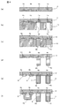
- FIGS. 1 is a sectional view of the module 1 according to the first embodiment
- FIG. 2 is an enlarged view of a region A in FIG. 1
- FIG. 3A is a plan view of the wiring board of the module 1
- FIG. It is an enlarged view of B area
- the module 1 includes a wiring board 2, a plurality of components 3 a and 3 b mounted on both main surfaces of the wiring board 2, and one main surface of the wiring board 2.
- the second sealing provided by covering the first sealing resin layer 7a (corresponding to the sealing resin layer of the present invention) thus formed, the other main surface of the wiring board 2, and the component 3b mounted on the other main surface.
- Mother board provided with various electronic devices It is mounted.
- the wiring board 2 is a multilayer wiring board formed of glass epoxy resin, low temperature co-fired ceramic (LTCC) or the like, and wiring electrodes (not shown) and via conductors (not shown) are formed on both main surfaces and inside thereof. ) Etc. are also formed.
- the wiring board 2 may have a single layer structure.
- Each substrate electrode 4a formed on one main surface of the wiring substrate 2 and each land electrode 4b formed on both main surfaces of the wiring substrate 2 are made of a metal such as Cu or Al (Cu in this embodiment). And is formed using a known electrode forming technique such as a printing technique or a photolithography technique. As shown in FIG. 2, Ni / Au plating 8 is applied to the mounting surface of each land electrode 4b with the components 3a and 3b.
- the area of the connection surface 4a1 connected to face the columnar conductor 5a of the substrate electrode 4a is an end surface on one end side which is a connection surface connected to face the substrate electrode 4a of the columnar conductor 5a. It is formed so as to be substantially the same as the area of 5a1.
- the components 3a and 3b mounted on both main surfaces of the wiring board 2 are composed of semiconductor components formed of Si, GaAs, or the like, or chip components such as a chip inductor or a chip capacitor, and use a known surface mounting technique. Then, it is mounted on both main surfaces of the wiring board 2.
- Each columnar conductor 5a is made of a metal such as Cu, and is formed on the substrate electrode 4a by electrolysis or electroless plating, and one end thereof is connected to the corresponding substrate electrode 4a.
- the columnar conductor 5a may be formed by plating growth on the substrate electrode 4a, or may be formed, for example, by connecting a pin-shaped conductor to the substrate electrode 4a with solder or the like.
- solder bumps 9 for connecting the module 1 to an external mother board are formed on the other end face of the columnar conductor 5a.
- the intermediate film 6 is made of a Ni / Au film and is provided on each columnar conductor 5a, and is connected to the outer peripheral surface of each columnar conductor 5a and the columnar conductor 5a of the substrate electrode 4a as shown in FIG. A portion of the connecting surface 4a1 that is not in contact with the columnar conductor 5a is covered. And in the state in which the 1st sealing resin layer 7a mentioned later was formed, the intermediate film 6 is interposed between the 1st sealing resin layer 7a and each columnar conductor 5a.
- the first and second sealing resin layers 7a and 7b are each formed of an epoxy resin or the like, and the first sealing resin layer 7a is an intermediate covering the one main surface of the wiring board 2 and the outer peripheral surface of each columnar conductor 5a.
- the coating 6 and each component 3a mounted on one main surface of the wiring substrate 2 are covered, and the second sealing resin layer 7b is formed on the other main surface of the wiring substrate 2 and each component 3b mounted on the other main surface. Is provided.
- each of the first and second sealing resin layers 7a and 7b can be formed using a coating method, a printing method, a compression mold method, a transfer mold method, or the like.
- the linear expansion coefficient is 7 to 14 ppm / ° C., and the linear expansion of each columnar conductor 5a and each substrate electrode 4a formed of Cu.
- Ni / Au film having a coefficient of 17 ppm / ° C., a linear expansion coefficient of each of the first and second sealing resin layers 7a and 7b of 5 to 13 ppm / ° C. (more preferably 5 to 10 ppm / ° C.), and forming the intermediate coating 6
- the linear expansion coefficient of Ni is 13 ppm / ° C. and Au is 14 ppm / ° C.
- the intermediate coating 6 has a linear expansion coefficient of the first sealing resin layer 7a and each columnar conductor 5a (or each substrate electrode 4a). ) Of the linear expansion coefficient.
- the wiring substrate 2 is made of glass epoxy resin or ceramic
- the columnar conductor 5a and the substrate electrode 4a are made of Cu. Therefore, among the interface between the columnar conductor 5a and the substrate electrode 4a and the interface between the wiring substrate 2 and the substrate electrode 4a, which is a connection portion between the wiring substrate 2 and the columnar conductor 5a, the interface between the columnar conductor 5a and the substrate electrode 4a is Cu Since the bonding between each other and the interface between the wiring substrate 2 and the substrate electrode 4a is a bonding between different materials of glass epoxy resin or ceramic and Cu, the adhesion strength between the interface between the wiring substrate 2 and the substrate electrode 4a is the same as that of the columnar conductor 5a.
- the adhesion strength at the interface of the substrate electrode 4a It is smaller than the adhesion strength at the interface of the substrate electrode 4a. Due to the recent demand for miniaturization of the module 1, the size of the substrate electrode 4a has been reduced. In this case, the contact area between the wiring substrate 2 and the substrate electrode 4a is reduced, and the wiring substrate 2 is further reduced. And the adhesion strength of the substrate electrode 4a are reduced.
- the stress when stress acts on the columnar conductor 5a at the periphery of the contact portion between the wiring substrate 2 and the substrate electrode 4a, which is a base point of the interface peeling between the wiring substrate 2 and the substrate electrode 4a, the stress is applied to the wiring.
- the arrangement is such that the interface peeling between the wiring substrate 2 and the substrate electrode 4a having a low adhesion strength can be prevented by disposing the substrate 2 and the columnar conductor 5a so as to be shifted in a predetermined direction from the place where the connection between the substrate 2 and the columnar conductor 5a works most strongly. Has been.
- This predetermined direction is caused by the difference in linear expansion coefficient between the mother substrate to which the other end of each columnar conductor 5a is connected and the first sealing resin layer 7a, and the columnar conductor 5a and the substrate electrode 4a at the time of low temperature change.
- the direction of the shear stress acting on the connection part is caused by the difference in linear expansion coefficient between the mother substrate to which the other end of each columnar conductor 5a is connected and the first sealing resin layer 7a, and the columnar conductor 5a and the substrate electrode 4a at the time of low temperature change.
- the module 1 is mounted on the mother board.
- the direction of the shear stress acting on the connection portion between the wiring board 2 and the columnar conductor 5a which is caused by the difference in shrinkage between the mother board and the first sealing resin layer 7a when the temperature is changed, is shown in FIG.
- the direction is the direction of the arrow, that is, the central direction of one main surface of the wiring board 2.
- the place where the shear stress becomes the strongest at this time is the edge of the one main surface of the wiring board 2 on the edge of the end surface 5a1 on the one end side of the columnar conductor 5a, that is, the end surface on one end side of the columnar conductor 5a.
- the peripheral edge of 5a1 when the arrow in FIG. 3B is extended in the direction opposite to the head of the arrow, it is in the vicinity of point P that intersects the outer periphery of the end face 5a1 on one end side of the columnar conductor 5a.
- the center point of the end surface 5a1 on one end side of the columnar conductor 5a is set to the center point of the connection surface 4a1 connected to face the columnar conductor 5a of the substrate electrode 4a.
- the wiring substrate 2 is arranged so as to be shifted toward the center of the one main surface.
- the columnar conductor 5a The amount of deviation is set to be larger as it is arranged on the edge side of the one main surface of the wiring board 2. It is not always necessary to change the amount of deviation according to the arrangement of the columnar conductors 5a, and the same amount of deviation may be set for all the columnar conductors 5a. Further, when the shear stress is decomposed into a component in the X direction and a component in the Y direction on one main surface of the wiring board 2 shown in FIG.
- the magnitude of the stress depends on the component in the X direction and the component in the Y direction.
- the shifting direction may be simplified, for example, by shifting each columnar conductor 5a in the X direction.
- the edge of one main surface of the wiring board 2 is set so that the center point of the end surface 5a1 on one end side of the columnar conductor 5a is opposite to the center point of the connection surface 4a1 connected to face the columnar conductor 5a of the substrate electrode 4a. It is good to displace in the direction.
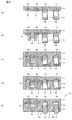
- FIG. 4 and FIG. 4 and 5 are views for explaining a method of manufacturing the module 1, and are partial cross-sectional views of the module 1 corresponding to FIG. 4A to 4F show each process of the manufacturing method, and FIGS. 5A to 5C show each process following FIG. 4F.
- each substrate electrode 4a and each land electrode 4b are formed on one main surface, and a plurality of land electrodes 4b each made of Cu are respectively formed on the other main surface.
- the formed wiring board 2 is prepared.
- each substrate electrode 4a and each land electrode 4b are formed using a known electrode forming technique such as a printing technique or a photolithography technique.
- the wiring board 2 has various wiring electrodes and via conductors formed on its main surface and inside.
- a hole 11 is formed at a place where the columnar conductor 5a of the resist 10 is formed using a photolithography technique or the like. Form.
- the center point of the end surface 5a1 on one end side of the columnar conductor 5a to be formed later is one main point of the wiring board 2 with respect to the center point of the connection surface 4a1 connected to face the columnar conductor 5a of the substrate electrode 4a.
- a hole 11 is formed in the resist 10 so as to be shifted toward the center of the surface.
- Ni / Au plating 8 is applied to the surface of each land electrode 4b formed on both main surfaces of the wiring board 2 together.
- each component 3a is mounted on one main surface of the wiring board 2 by using a known surface mounting technique, and as shown in FIG.
- a first sealing resin layer 7 a that covers each component 3 a and the intermediate coating 6 mounted on one main surface of the wiring substrate 2 is formed.
- the first sealing resin layer 7a can be formed using a coating method, a printing method, a compression mold method, a transfer mold method, or the like.
- a second sealing resin layer 7b covering the other main surface of the wiring substrate 2 and each component 3b is formed.
- the second sealing resin layer 7b can also be formed using the same method as the first sealing resin layer 7a.
- the module 1 is manufactured by forming the solder bumps 9 on the end surfaces of the exposed columnar conductors 5a on the other end side.
- a Ni / Au film may be formed on the end face on the other end side of each columnar conductor 5a again.
- each component 3b on the other main surface of the wiring board 2 is performed before and after the mounting of each component 3a on the one main surface of the wiring board 2, and then the first and second sealing resin layers 7a, 7b may be formed simultaneously. Further, after polishing or grinding the surface of the first sealing resin layer 7a, each component 3b is mounted on the other main surface of the wiring board 2, and then the second sealing resin layer 7b is formed. Good.
- the intermediate coating 6 is interposed between the first sealing resin layer 7a and each columnar conductor 5a, for example, when the module 1 is mounted on an external mother substrate, the mother substrate Even if stress is applied to each columnar conductor 5a due to the difference in linear expansion coefficient (difference in expansion / contraction) between the first sealing resin layer 7a of the module 1 and the first sealing resin layer 7a, The stress acting on each columnar conductor 5a can be relaxed by functioning as a relaxation material.
- the stress acting on the columnar conductor 5a prevents peeling at the interface between the wiring substrate 2 and the substrate electrode 4a or the interface between the substrate electrode 4a and the columnar conductor 5a at the connection portion between the columnar conductor 5a and the wiring substrate 2. can do.
- the intermediate coating 6 has a linear expansion coefficient between the linear expansion coefficient of the columnar conductor 5a and the linear expansion coefficient of the first sealing resin layer 7a, the columnar conductor 5a is not sealed by the intermediate coating 6 and is first sealed. Compared with the conventional module sealed with the stop resin layer 7a, the difference in linear expansion coefficient between the columnar conductor 5a and the intermediate coating 6, and between the intermediate coating 6 and the first sealing resin layer 7a is reduced.
- each columnar conductor 5a stress acting on each columnar conductor 5a concentrates on the connection portion between the wiring board 2 and the columnar conductor 5a due to the interface peeling between each columnar conductor 5a and the first sealing resin layer 7a as in the conventional module.
- the interface peeling between the wiring board 2 and the substrate electrode 4a and the interface peeling between the substrate electrode 4a and the columnar conductor 5a can be prevented.
- the module 1 having high connection reliability with the outside can be provided.
- each columnar conductor 5a when stress acts on the peripheral edge of the portion where the wiring substrate 2 and the substrate electrode 4a are in contact with each other and the columnar conductor 5a, which is a base point of the interface peeling between the wiring substrate 2 and the substrate electrode 4a.
- the columnar conductor 5a and the wiring board 2 are connected to each other so that the shear stress acting on the connection portion between the columnar conductor 5a and the peripheral edge of the end surface 5a1 on one end side of the columnar conductor 5a (see point P in FIG. 3B) is separated.
- the intermediate coating 6 is formed of a Ni / Au film, it is practical because the intermediate coating 6 can be formed by plating. Further, since the metal has ductility, the intermediate coating 6 can function as a cushioning material that relieves stress on each columnar conductor 5a that acts due to expansion / contraction of the first sealing resin layer 7a.
- the intermediate coating 6 is provided so as to cover a portion of the connection surface 4a1 that is connected to the columnar conductor 5a of the substrate electrode 4a so as not to contact the columnar conductor 5a,
- the intermediate coating 6 is interposed between the first sealing resin layer 7a and a portion of the connection surface 4a1 that is connected to face the columnar conductor 5a and is not in contact with the columnar conductor 5a. Therefore, the stress acting on the interface between the wiring substrate 2 and the substrate electrode 4a is relieved by the intermediate coating 6 due to the expansion / contraction of the first sealing resin layer 7a. Can be further reduced.
- the intermediate coating 6 since the intermediate coating 6 has a linear expansion coefficient between the linear expansion coefficient of the substrate electrode 4a and the linear expansion coefficient of the first sealing resin layer 7a, the intermediate coating 6 has an interface between the intermediate coating 6 and the substrate electrode 4a when the temperature changes.
- the working stress and the stress acting on the interface between the intermediate coating 6 and the first sealing resin layer 7a can be reduced, and the adhesion characteristics at both interfaces are improved.
- the area of the connection surface 4a1 connected to be opposed to the columnar conductor 5a of the substrate electrode 4a is substantially the same as the area of the end surface 5a1 on one end side of the columnar conductor 5a. Since the size of the electrode 4a in plan view can be reduced and the substrate electrodes 4a can be arranged at a narrow pitch, the module 1 can be reduced in size while ensuring the connection reliability between the module 1 and an external mother board or the like. Can be achieved.
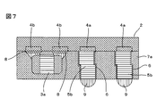
- FIGS. 6 is a cross-sectional view of the module 1a
- FIG. 7 is an enlarged view of a region C in FIG.
- the module 1a according to this embodiment is different from the module 1 according to the first embodiment described with reference to FIGS. 1 to 3 in that each columnar conductor 5b is different from that shown in FIGS. This is a point having a step in the length direction. Since other configurations are the same as those of the module 1 of the first embodiment, the description thereof is omitted by attaching the same reference numerals.
- each columnar conductor 5 b is provided with a step in the length direction, and the outer peripheral surface thereof is covered with the intermediate coating 6. Further, assuming that the linear expansion coefficient of the mother substrate to which the other end of each columnar conductor 5b is connected is larger than the linear expansion coefficient of the first sealing resin layer 7a, the same as the module 1 of the first embodiment. Further, in each columnar conductor 5b, the center point of the end surface on one end side of the columnar conductor 5b connected to face the substrate electrode 4a is the center of the connection surface connected to face the columnar conductor 5b of the substrate electrode 4a. With respect to the point, the wiring substrate 2 is arranged so as to be shifted in the central direction of the one main surface.
- FIG. 8 and FIG. 8 and 9 are views for explaining a method of manufacturing the module 1a, and are partial cross-sectional views of the module 1a corresponding to FIG. 8A to 8F show each process of the manufacturing method, and FIGS. 9A to 9E show each process following FIG. 8F.
- each substrate electrode 4a and each land electrode 4b are formed on one main surface, and a plurality of land electrodes 4b each made of Cu are respectively formed on the other main surface.
- the formed wiring board 2 is prepared.
- each substrate electrode 4a and each land electrode 4b are formed using a known electrode forming technique such as a printing technique or a photolithography technique.
- the wiring board 2 has various wiring electrodes and via conductors formed on its main surface and inside.
- a first-stage resist 12a is formed on one main surface of the wiring board 2, and then a columnar conductor 5b of the resist 12a is formed using a photolithography technique or the like.
- a first-stage hole 13a is formed at the location.
- the center point of the end surface on one end side of the columnar conductor 5b to be formed later is the center point of the connection surface connected to the columnar conductor 5b of the substrate electrode 4a so as to face the one main surface of the wiring board 2.
- a hole 13a is formed in the resist 12a so as to be shifted from the center. Further, the resist 12a is formed so that the thickness of the resist 12a at this time is thinner than the target length of each columnar conductor 5b.
- the first stage portion 5b1 of the columnar conductor 5b made of Cu is formed by plating or the like.
- the columnar conductors 5b are formed by using a photolithography technique or the like.
- a hole 13b for forming the second-stage portion 5b2 is formed in the resist 12b.
- the second-stage hole 13b is perpendicular to the length direction of the columnar conductor 5b with respect to the first-stage hole 13a so that a step is formed in the length direction of the columnar conductor 5b.
- the substrate 2 is arranged so as to be shifted to the edge side of the one main surface. Note that the direction in which the second-stage hole 13b is shifted is not limited to the edge side of the one main surface of the wiring board 2, and may be changed to the center side of the wiring board 2, for example.
- a second-stage portion 5b2 is formed in the same manner as the first-stage portion 5b1 of the columnar conductor 5b, and as shown in FIG. The resist 12a and the second-stage resist 12b are removed.
- the Ni / Au plating 8 on the intermediate coating 6 and each land electrode 4b is processed in the same manner as the manufacturing method of the module 1 of the first embodiment. Formation (see FIG. 9A), mounting of each component 3a on one main surface of the wiring board 2 (see FIG. 9B), formation of the first sealing resin layer 7a (see FIG. 9C), Mounting each component 3b on the other main surface of the wiring board 2, forming the second sealing resin layer 7b, polishing or grinding the surface of the first sealing resin layer 7a (see FIG. 9D), each columnar conductor
- the module 1a is manufactured by forming the solder bumps 9 on the end face on the other end side of 5b (see FIG. 9E).
- each columnar conductor 5b by providing a step in the length direction of each columnar conductor 5b, the contact area between the columnar conductor 5b and the intermediate coating 6 and the intermediate coating 6 are provided by the amount of the step. Since the contact area between the first sealing resin layer 7a and the first sealing resin layer 7a increases, the adhesion strength at these interfaces is improved. Moreover, since the movement in the length direction of each columnar conductor 5b is restricted by the step, for example, a mother board is arranged below the module 1a, and the other end of each columnar conductor 5b and the mother board are connected. When connected, each columnar conductor 5b can be prevented from falling off to the mother substrate side.
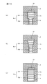
- FIG. 10A to 10C are cross-sectional views of the columnar conductors 5c to 5e according to this example.
- the cross-sectional area of the first stage portion 5c1 of the columnar conductor 5c connected to the substrate electrode 4a is provided on the mother substrate while providing a step in the length direction of the columnar conductor 5c. It may be larger than the second stage portion 5c2 of the columnar conductor 5c to be connected.
- the first step portion 5d1 of the columnar conductor 5d is formed in a tapered shape whose cross-sectional area decreases as it goes down in the drawing, and the second step of the columnar conductor 5d.
- the cross-sectional area of the portion 5d2 may be smaller than that of the first-stage portion 5d1.
- a convex portion 14 may be provided at the boundary between the first step portion 5e1 and the second step portion 5e2 of the outer peripheral surface of the columnar conductor 5e.
- each columnar conductor 5c to 5e has a circular shape in the cross section of the first stage portions 5c1 to 5e1, and each columnar conductor has a rectangular shape in the cross section of the second stage portions 5c2 to 5e2.
- the cross-sectional shapes of the first-stage portions 5c1 to 5e2 of 5c to 5e and the second-stage portions 5c2 to 5e2 may be changed.
- the cross-sectional areas of the first-stage portions 5c1 and 5d1 on one end side of the columnar conductors 5c and 5d are set to be equal to those of the columnar conductors 5c and 5d.
- the present invention is not limited to the above-described embodiments, and various modifications other than those described above can be made without departing from the spirit thereof.
- the module of the second embodiment Although 1a demonstrated the case where one level
- the columnar conductor may be formed of a conductive paste or a metal pin in addition to the formation by plating.
- the columnar conductors 5a and 5b are arranged to be shifted in a predetermined direction with respect to the substrate electrode 4a.
- solder bump 9 it is not necessary to form the solder bump 9 on the end face on the other end side connected to the mother substrate of the columnar conductors 5a to 5e.
- the present invention can be applied to various modules in which a columnar conductor for external connection connected to a wiring board is sealed with resin.
Landscapes
- Engineering & Computer Science (AREA)
- Microelectronics & Electronic Packaging (AREA)
- Manufacturing & Machinery (AREA)
- Printing Elements For Providing Electric Connections Between Printed Circuits (AREA)
- Structures Or Materials For Encapsulating Or Coating Semiconductor Devices Or Solid State Devices (AREA)
- Combinations Of Printed Boards (AREA)
- Surface Acoustic Wave Elements And Circuit Networks Thereof (AREA)
Abstract
Priority Applications (3)
| Application Number | Priority Date | Filing Date | Title |
|---|---|---|---|
| JP2015518125A JP6137309B2 (ja) | 2013-05-21 | 2014-03-10 | モジュール |
| CN201480029008.9A CN105230135B (zh) | 2013-05-21 | 2014-03-10 | 模块 |
| US14/943,245 US9832871B2 (en) | 2013-05-21 | 2015-11-17 | Module |
Applications Claiming Priority (2)
| Application Number | Priority Date | Filing Date | Title |
|---|---|---|---|
| JP2013-107346 | 2013-05-21 | ||
| JP2013107346 | 2013-05-21 |
Related Child Applications (1)
| Application Number | Title | Priority Date | Filing Date |
|---|---|---|---|
| US14/943,245 Continuation US9832871B2 (en) | 2013-05-21 | 2015-11-17 | Module |
Publications (1)
| Publication Number | Publication Date |
|---|---|
| WO2014188760A1 true WO2014188760A1 (fr) | 2014-11-27 |
Family
ID=51933326
Family Applications (1)
| Application Number | Title | Priority Date | Filing Date |
|---|---|---|---|
| PCT/JP2014/056192 Ceased WO2014188760A1 (fr) | 2013-05-21 | 2014-03-10 | Module |
Country Status (4)
| Country | Link |
|---|---|
| US (1) | US9832871B2 (fr) |
| JP (1) | JP6137309B2 (fr) |
| CN (1) | CN105230135B (fr) |
| WO (1) | WO2014188760A1 (fr) |
Cited By (9)
| Publication number | Priority date | Publication date | Assignee | Title |
|---|---|---|---|---|
| JP2017204635A (ja) * | 2016-05-11 | 2017-11-16 | 日月光半導体製造股▲ふん▼有限公司 | 半導体装置パッケージ及びその製造方法 |
| WO2018003391A1 (fr) * | 2016-06-29 | 2018-01-04 | 株式会社村田製作所 | Substrat à composants intégrés, son procédé de fabrication et module haute fréquence |
| WO2018168709A1 (fr) * | 2017-03-14 | 2018-09-20 | 株式会社村田製作所 | Module de circuit et procédé pour sa production |
| WO2018230534A1 (fr) * | 2017-06-16 | 2018-12-20 | 株式会社村田製作所 | Carte de circuit imprimé, module de circuit, procédé de production de carte de circuit imprimé et procédé de production de module de circuit |
| WO2019059017A1 (fr) * | 2017-09-20 | 2019-03-28 | 株式会社村田製作所 | Procédé de production d'un substrat céramique, substrat céramique et module |
| WO2020066380A1 (fr) * | 2018-09-28 | 2020-04-02 | 株式会社村田製作所 | Module de circuit et dispositif de communication |
| WO2023074262A1 (fr) * | 2021-11-01 | 2023-05-04 | 株式会社村田製作所 | Module de circuit |
| WO2025121100A1 (fr) * | 2023-12-04 | 2025-06-12 | 株式会社村田製作所 | Module de circuit |
| WO2025121101A1 (fr) * | 2023-12-04 | 2025-06-12 | 株式会社村田製作所 | Module de circuit |
Families Citing this family (4)
| Publication number | Priority date | Publication date | Assignee | Title |
|---|---|---|---|---|
| JP6520801B2 (ja) * | 2016-04-19 | 2019-05-29 | 株式会社村田製作所 | 電子部品 |
| JP6512161B2 (ja) * | 2016-04-21 | 2019-05-15 | 株式会社村田製作所 | 電子部品 |
| JP7443168B2 (ja) * | 2020-06-26 | 2024-03-05 | NDK SAW devices株式会社 | 弾性表面波デバイス |
| EP4333565A1 (fr) * | 2022-09-01 | 2024-03-06 | Murata Manufacturing Co., Ltd. | Composant électronique à contrainte réduite |
Citations (5)
| Publication number | Priority date | Publication date | Assignee | Title |
|---|---|---|---|---|
| JPH11121645A (ja) * | 1997-10-14 | 1999-04-30 | Matsushita Electric Ind Co Ltd | セラミック多層基板及びその製造方法 |
| JP2003023253A (ja) * | 2001-07-10 | 2003-01-24 | Ibiden Co Ltd | 多層プリント配線板 |
| JP2005159268A (ja) * | 2003-10-29 | 2005-06-16 | Kyocera Corp | 配線基板及びその製造方法 |
| JP2012138628A (ja) * | 2012-04-02 | 2012-07-19 | Fujitsu Semiconductor Ltd | 配線基板及び半導体装置 |
| WO2013035717A1 (fr) * | 2011-09-07 | 2013-03-14 | 株式会社村田製作所 | Module et procédé de fabrication associé |
Family Cites Families (15)
| Publication number | Priority date | Publication date | Assignee | Title |
|---|---|---|---|---|
| US4131516A (en) * | 1977-07-21 | 1978-12-26 | International Business Machines Corporation | Method of making metal filled via holes in ceramic circuit boards |
| JP2001217346A (ja) * | 2000-02-04 | 2001-08-10 | Pfu Ltd | 小型半導体の実装構造および小型半導体装置 |
| JP2001237537A (ja) * | 2000-02-25 | 2001-08-31 | Pfu Ltd | 小型半導体の実装構造および小型半導体装置 |
| KR100917081B1 (ko) | 2001-03-14 | 2009-09-15 | 이비덴 가부시키가이샤 | 다층 프린트 배선판 |
| JP4639101B2 (ja) * | 2004-03-31 | 2011-02-23 | 日本特殊陶業株式会社 | 部品支持基板及びその製造方法、光デバイス |
| JP2006012870A (ja) | 2004-06-22 | 2006-01-12 | Satoshi Ishiguro | スタックビア構造多層配線基板の製造方法 |
| JP4387269B2 (ja) | 2004-08-23 | 2009-12-16 | 株式会社テクニスコ | ビアが形成されたガラス基板及びビアの形成方法 |
| JPWO2006035528A1 (ja) * | 2004-09-29 | 2008-05-15 | 株式会社村田製作所 | スタックモジュール及びその製造方法 |
| WO2006051821A1 (fr) * | 2004-11-10 | 2006-05-18 | Murata Manufacturing Co., Ltd. | Substrat multicouche céramique et procédé de fabrication idoine |
| KR100952171B1 (ko) * | 2005-10-20 | 2010-04-09 | 가부시키가이샤 무라타 세이사쿠쇼 | 회로 모듈 및 이 회로 모듈을 사용한 회로 장치 |
| JP5324051B2 (ja) * | 2007-03-29 | 2013-10-23 | 新光電気工業株式会社 | 配線基板の製造方法及び半導体装置の製造方法及び配線基板 |
| JP5032187B2 (ja) * | 2007-04-17 | 2012-09-26 | 新光電気工業株式会社 | 配線基板の製造方法及び半導体装置の製造方法及び配線基板 |
| US8030752B2 (en) * | 2007-12-18 | 2011-10-04 | Samsung Electro-Mechanics Co., Ltd. | Method of manufacturing semiconductor package and semiconductor plastic package using the same |
| JP2011222928A (ja) * | 2010-03-26 | 2011-11-04 | Kyocera Corp | 配線基板およびプローブカード |
| WO2012125331A1 (fr) * | 2011-03-11 | 2012-09-20 | Hsio Technologies, Llc | Structure de circuit électrique à trous d'interconnexion blindés à piliers de cuivre |
-
2014
- 2014-03-10 WO PCT/JP2014/056192 patent/WO2014188760A1/fr not_active Ceased
- 2014-03-10 JP JP2015518125A patent/JP6137309B2/ja active Active
- 2014-03-10 CN CN201480029008.9A patent/CN105230135B/zh active Active
-
2015
- 2015-11-17 US US14/943,245 patent/US9832871B2/en active Active
Patent Citations (5)
| Publication number | Priority date | Publication date | Assignee | Title |
|---|---|---|---|---|
| JPH11121645A (ja) * | 1997-10-14 | 1999-04-30 | Matsushita Electric Ind Co Ltd | セラミック多層基板及びその製造方法 |
| JP2003023253A (ja) * | 2001-07-10 | 2003-01-24 | Ibiden Co Ltd | 多層プリント配線板 |
| JP2005159268A (ja) * | 2003-10-29 | 2005-06-16 | Kyocera Corp | 配線基板及びその製造方法 |
| WO2013035717A1 (fr) * | 2011-09-07 | 2013-03-14 | 株式会社村田製作所 | Module et procédé de fabrication associé |
| JP2012138628A (ja) * | 2012-04-02 | 2012-07-19 | Fujitsu Semiconductor Ltd | 配線基板及び半導体装置 |
Cited By (19)
| Publication number | Priority date | Publication date | Assignee | Title |
|---|---|---|---|---|
| JP2017204635A (ja) * | 2016-05-11 | 2017-11-16 | 日月光半導体製造股▲ふん▼有限公司 | 半導体装置パッケージ及びその製造方法 |
| US10446411B2 (en) | 2016-05-11 | 2019-10-15 | Advanced Semiconductor Engineering, Inc. | Semiconductor device package with a conductive post |
| WO2018003391A1 (fr) * | 2016-06-29 | 2018-01-04 | 株式会社村田製作所 | Substrat à composants intégrés, son procédé de fabrication et module haute fréquence |
| US10707172B2 (en) | 2016-06-29 | 2020-07-07 | Murata Manufacturing Co., Ltd. | Component-embedded substrate, method of manufacturing the same, and high-frequency module |
| WO2018168709A1 (fr) * | 2017-03-14 | 2018-09-20 | 株式会社村田製作所 | Module de circuit et procédé pour sa production |
| CN110402491A (zh) * | 2017-03-14 | 2019-11-01 | 株式会社村田制作所 | 电路模块及其制造方法 |
| CN110402491B (zh) * | 2017-03-14 | 2022-11-18 | 株式会社村田制作所 | 电路模块及其制造方法 |
| US10660207B2 (en) | 2017-03-14 | 2020-05-19 | Murata Manufacturing Co., Ltd. | Circuit module and method for manufacturing the same |
| US11310914B2 (en) | 2017-06-16 | 2022-04-19 | Murata Manufacturing Co., Ltd. | Circuit board, circuit module, method of manufacturing circuit board, and method of manufacturing circuit module |
| WO2018230534A1 (fr) * | 2017-06-16 | 2018-12-20 | 株式会社村田製作所 | Carte de circuit imprimé, module de circuit, procédé de production de carte de circuit imprimé et procédé de production de module de circuit |
| WO2019059017A1 (fr) * | 2017-09-20 | 2019-03-28 | 株式会社村田製作所 | Procédé de production d'un substrat céramique, substrat céramique et module |
| US10854385B2 (en) | 2017-09-20 | 2020-12-01 | Murata Manufacturing Co., Ltd. | Method for producing ceramic substrate, ceramic substrate, and module |
| JP7031678B2 (ja) | 2017-09-20 | 2022-03-08 | 株式会社村田製作所 | セラミック基板の製造方法、セラミック基板、及び、モジュール |
| JPWO2019059017A1 (ja) * | 2017-09-20 | 2020-10-01 | 株式会社村田製作所 | セラミック基板の製造方法、セラミック基板、及び、モジュール |
| WO2020066380A1 (fr) * | 2018-09-28 | 2020-04-02 | 株式会社村田製作所 | Module de circuit et dispositif de communication |
| US11817358B2 (en) | 2018-09-28 | 2023-11-14 | Murata Manufacturing Co., Ltd. | Circuit module and communication device |
| WO2023074262A1 (fr) * | 2021-11-01 | 2023-05-04 | 株式会社村田製作所 | Module de circuit |
| WO2025121100A1 (fr) * | 2023-12-04 | 2025-06-12 | 株式会社村田製作所 | Module de circuit |
| WO2025121101A1 (fr) * | 2023-12-04 | 2025-06-12 | 株式会社村田製作所 | Module de circuit |
Also Published As
| Publication number | Publication date |
|---|---|
| JP6137309B2 (ja) | 2017-05-31 |
| US20160073499A1 (en) | 2016-03-10 |
| CN105230135B (zh) | 2018-04-20 |
| CN105230135A (zh) | 2016-01-06 |
| US9832871B2 (en) | 2017-11-28 |
| JPWO2014188760A1 (ja) | 2017-02-23 |
Similar Documents
| Publication | Publication Date | Title |
|---|---|---|
| JP6137309B2 (ja) | モジュール | |
| JP5790682B2 (ja) | モジュールおよびその製造方法 | |
| CN100508701C (zh) | 复合多层基板及其制造方法 | |
| US8123965B2 (en) | Interconnect structure with stress buffering ability and the manufacturing method thereof | |
| JP5367523B2 (ja) | 配線基板及び配線基板の製造方法 | |
| US8163596B2 (en) | Stackable electronic package and method of making same | |
| CN111328427A (zh) | 配线基板、半导体装置以及配线基板的制造方法 | |
| CN111345121A (zh) | 玻璃配线基板、其制造方法以及半导体装置 | |
| JP6981537B2 (ja) | 高周波モジュール | |
| EP2775523A1 (fr) | Boîtier BGA de puce retournée (PMIC et IPD passifs) avec fixation de puce sur puce utilisant un nouveau substrat de cavité BGA | |
| KR20100086472A (ko) | 다층 배선 요소와 마이크로전자 요소가 실장된 어셈블리 | |
| US11335648B2 (en) | Semiconductor chip fabrication and packaging methods thereof | |
| US20040156177A1 (en) | Package of electronic components and method for producing the same | |
| WO2019111873A1 (fr) | Module | |
| WO2023189540A1 (fr) | Carte de câblage en verre, son procédé de fabrication, et dispositif d'imagerie | |
| WO2018168709A1 (fr) | Module de circuit et procédé pour sa production | |
| US5843810A (en) | Film circuit and method of manufacturing the same | |
| US20220181244A1 (en) | Package substrate and package structure | |
| US11004759B2 (en) | Electronic component and method for manufacturing the same | |
| JP2004266271A (ja) | 電子部品の実装体及びその製造方法 | |
| JP2007311492A (ja) | 半導体装置の製造方法 | |
| JP2005340355A (ja) | 配線基板 | |
| US20050005436A1 (en) | Method for preparing thin integrated circuits with multiple circuit layers | |
| JP2019071322A (ja) | 配線基板、電子装置、及び、配線基板の製造方法 | |
| US20140118977A1 (en) | Wiring board |
Legal Events
| Date | Code | Title | Description |
|---|---|---|---|
| WWE | Wipo information: entry into national phase |
Ref document number: 201480029008.9 Country of ref document: CN |
|
| 121 | Ep: the epo has been informed by wipo that ep was designated in this application |
Ref document number: 14801107 Country of ref document: EP Kind code of ref document: A1 |
|
| ENP | Entry into the national phase |
Ref document number: 2015518125 Country of ref document: JP Kind code of ref document: A |
|
| NENP | Non-entry into the national phase |
Ref country code: DE |
|
| 122 | Ep: pct application non-entry in european phase |
Ref document number: 14801107 Country of ref document: EP Kind code of ref document: A1 |