WO2014189105A1 - Module d'ondes millimétriques - Google Patents
Module d'ondes millimétriques Download PDFInfo
- Publication number
- WO2014189105A1 WO2014189105A1 PCT/JP2014/063581 JP2014063581W WO2014189105A1 WO 2014189105 A1 WO2014189105 A1 WO 2014189105A1 JP 2014063581 W JP2014063581 W JP 2014063581W WO 2014189105 A1 WO2014189105 A1 WO 2014189105A1
- Authority
- WO
- WIPO (PCT)
- Prior art keywords
- dielectric substrate
- millimeter wave
- multilayer dielectric
- cap
- wave module
- Prior art date
- Legal status (The legal status is an assumption and is not a legal conclusion. Google has not performed a legal analysis and makes no representation as to the accuracy of the status listed.)
- Ceased
Links
Images

Classifications
-
- H—ELECTRICITY
- H01—ELECTRIC ELEMENTS
- H01P—WAVEGUIDES; RESONATORS, LINES, OR OTHER DEVICES OF THE WAVEGUIDE TYPE
- H01P5/00—Coupling devices of the waveguide type
- H01P5/08—Coupling devices of the waveguide type for linking dissimilar lines or devices
- H01P5/10—Coupling devices of the waveguide type for linking dissimilar lines or devices for coupling balanced lines or devices with unbalanced lines or devices
- H01P5/107—Hollow-waveguide/strip-line transitions
-
- H—ELECTRICITY
- H10—SEMICONDUCTOR DEVICES; ELECTRIC SOLID-STATE DEVICES NOT OTHERWISE PROVIDED FOR
- H10W—GENERIC PACKAGES, INTERCONNECTIONS, CONNECTORS OR OTHER CONSTRUCTIONAL DETAILS OF DEVICES COVERED BY CLASS H10
- H10W44/00—Electrical arrangements for controlling or matching impedance
- H10W44/20—Electrical arrangements for controlling or matching impedance at high-frequency [HF] or radio frequency [RF]
-
- H—ELECTRICITY
- H01—ELECTRIC ELEMENTS
- H01P—WAVEGUIDES; RESONATORS, LINES, OR OTHER DEVICES OF THE WAVEGUIDE TYPE
- H01P5/00—Coupling devices of the waveguide type
- H01P5/02—Coupling devices of the waveguide type with invariable factor of coupling
- H01P5/022—Transitions between lines of the same kind and shape, but with different dimensions
- H01P5/028—Transitions between lines of the same kind and shape, but with different dimensions between strip lines
-
- H—ELECTRICITY
- H10—SEMICONDUCTOR DEVICES; ELECTRIC SOLID-STATE DEVICES NOT OTHERWISE PROVIDED FOR
- H10W—GENERIC PACKAGES, INTERCONNECTIONS, CONNECTORS OR OTHER CONSTRUCTIONAL DETAILS OF DEVICES COVERED BY CLASS H10
- H10W40/00—Arrangements for thermal protection or thermal control
- H10W40/20—Arrangements for cooling
- H10W40/231—Arrangements for cooling characterised by their places of attachment or cooling paths
-
- H—ELECTRICITY
- H10—SEMICONDUCTOR DEVICES; ELECTRIC SOLID-STATE DEVICES NOT OTHERWISE PROVIDED FOR
- H10W—GENERIC PACKAGES, INTERCONNECTIONS, CONNECTORS OR OTHER CONSTRUCTIONAL DETAILS OF DEVICES COVERED BY CLASS H10
- H10W44/00—Electrical arrangements for controlling or matching impedance
- H10W44/20—Electrical arrangements for controlling or matching impedance at high-frequency [HF] or radio frequency [RF]
- H10W44/203—Electrical connections
- H10W44/216—Waveguides, e.g. strip lines
-
- H—ELECTRICITY
- H10—SEMICONDUCTOR DEVICES; ELECTRIC SOLID-STATE DEVICES NOT OTHERWISE PROVIDED FOR
- H10W—GENERIC PACKAGES, INTERCONNECTIONS, CONNECTORS OR OTHER CONSTRUCTIONAL DETAILS OF DEVICES COVERED BY CLASS H10
- H10W44/00—Electrical arrangements for controlling or matching impedance
- H10W44/20—Electrical arrangements for controlling or matching impedance at high-frequency [HF] or radio frequency [RF]
- H10W44/251—Electrical arrangements for controlling or matching impedance at high-frequency [HF] or radio frequency [RF] for monolithic microwave integrated circuits [MMIC]
-
- H—ELECTRICITY
- H10—SEMICONDUCTOR DEVICES; ELECTRIC SOLID-STATE DEVICES NOT OTHERWISE PROVIDED FOR
- H10W—GENERIC PACKAGES, INTERCONNECTIONS, CONNECTORS OR OTHER CONSTRUCTIONAL DETAILS OF DEVICES COVERED BY CLASS H10
- H10W70/00—Package substrates; Interposers; Redistribution layers [RDL]
- H10W70/60—Insulating or insulated package substrates; Interposers; Redistribution layers
-
- H—ELECTRICITY
- H10—SEMICONDUCTOR DEVICES; ELECTRIC SOLID-STATE DEVICES NOT OTHERWISE PROVIDED FOR
- H10W—GENERIC PACKAGES, INTERCONNECTIONS, CONNECTORS OR OTHER CONSTRUCTIONAL DETAILS OF DEVICES COVERED BY CLASS H10
- H10W90/00—Package configurations
- H10W90/701—Package configurations characterised by the relative positions of pads or connectors relative to package parts
- H10W90/751—Package configurations characterised by the relative positions of pads or connectors relative to package parts of bond wires
- H10W90/753—Package configurations characterised by the relative positions of pads or connectors relative to package parts of bond wires between laterally-adjacent chips
-
- H—ELECTRICITY
- H10—SEMICONDUCTOR DEVICES; ELECTRIC SOLID-STATE DEVICES NOT OTHERWISE PROVIDED FOR
- H10W—GENERIC PACKAGES, INTERCONNECTIONS, CONNECTORS OR OTHER CONSTRUCTIONAL DETAILS OF DEVICES COVERED BY CLASS H10
- H10W90/00—Package configurations
- H10W90/701—Package configurations characterised by the relative positions of pads or connectors relative to package parts
- H10W90/751—Package configurations characterised by the relative positions of pads or connectors relative to package parts of bond wires
- H10W90/754—Package configurations characterised by the relative positions of pads or connectors relative to package parts of bond wires between a chip and a stacked insulating package substrate, interposer or RDL
Definitions
- the present invention relates to a structure of a high frequency circuit (referred to as a millimeter wave module) in the millimeter wave band.
- a millimeter wave module a high frequency circuit in the millimeter wave band.
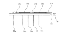
- FIG. 1a is a plan view of a conventional millimeter wave module
- FIG. 1b is a cross-sectional view thereof.
- the conventional millimeter wave module includes a plurality of MMICs (Monolithic Microwave IC) 30a, 30b and a dielectric material transmission line 20a, 20b, 20c connecting them to a metal base 10. It is configured by mounting. At this time, it is necessary to provide pins 50a to 50e on the metal base 10 in order to supply power to the MMIC, or to connect the IF signal (intermediate frequency signal) and LO signal (local signal) to an external circuit.
- MMICs Monitoring Microwave IC
- the connection portion of the millimeter wave signal has a waveguide structure.
- the connection portion of the millimeter wave signal has a waveguide structure.
- FIGS. 1 a and 1 b holes for forming the waveguide 60 are processed in the metal base 10.
- a metal base on which the millimeter wave circuit is mounted is provided with pins for connecting signals to the outside, It was necessary to provide a matching waveguide. In order to provide pins and holes, it is necessary to prepare molds and equipment that process metal bases with high precision, and flexibility when changing specifications to millimeter wave circuits for other frequency bands is extremely high It was low. Such a conventional structure has been one of the factors hindering the realization of a low-cost millimeter-wave module because it develops dedicated equipment and manufacturing methods for each frequency.
- Patent Documents 1 to 3 have a structure in which a recess for housing an MMIC is processed in a multilayer substrate on which a millimeter wave circuit is mounted, and a metal cover that covers the opening of the recess is bonded and fixed on the multilayer substrate. It has been. That is, the devices disclosed in these documents are also very low in flexibility when changing specifications to millimeter wave circuits for other frequency bands, and it is difficult to reduce the cost of the millimeter wave module.
- An example of the object of the present invention is to provide a structure capable of realizing an inexpensive millimeter-wave module in view of the above-described problems.
- the present invention relates to a millimeter wave module including a millimeter wave circuit composed of a plurality of MMICs and a transmission line connecting them, and a metal base on which the millimeter wave circuit is mounted.
- One embodiment of the present invention includes a multilayer dielectric substrate placed on a base, a metal cap, and a screwing member screwed into the cap or the base. The state where the multilayer dielectric substrate is sandwiched between the cap and the base is maintained by tightening the screwing member.
- a plurality of MMICs constituting the millimeter wave circuit and a transmission line connecting them are mounted on the surface layer of the multilayer dielectric substrate, and terminals for signal connection to the outside of the millimeter wave module (for example, power supply, LO signal, And IF signal connection terminals) are disposed on the periphery of the multilayer dielectric substrate.
- the cap is disposed on the surface layer of the multilayer dielectric substrate, and is configured to expose the peripheral terminal of the multilayer dielectric substrate to cover the MMIC and the transmission line.
- a plurality of MMICs constituting a millimeter wave circuit and a transmission line connecting them are mounted on a general multilayer dielectric substrate, and a terminal for connecting a signal to the outside of the millimeter wave module is provided as a multilayer dielectric.
- a structure is provided in which the multilayer dielectric substrate is sandwiched between a metal base and a cap and fastened with a screwing member such as a screw.
- the top view which shows the structure of the conventional millimeter wave module.
- Sectional drawing which shows the structure of the conventional millimeter wave module.
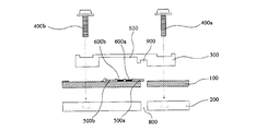
- Sectional drawing which shows the millimeter wave module by one embodiment of this invention.
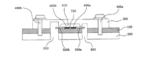
- Sectional drawing which shows the structure of the millimeter wave module of the aspect of FIG.
- Multi-layer dielectric substrate 110 Holes 111a, 112a, 113a, 114a, 115a, 111b, 112b, 113b, 114b, 115b which are part of the waveguide 120 Terminal 120 Through hole 140a, 140b, 150 Inner layer of multi-layer substrate Wiring 200 Metal base 300 Cap 400a, 400b Screw 500a, 500b Dielectric substrates 600a, 600b MMIC as transmission lines 700a, 700b Capacitor 750 Bonding wire (gold wire) 800,850 Waveguide 900 Short surface
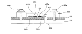
- FIG. 2 is a cross-sectional view of a millimeter wave module according to an embodiment of the present invention.
- the millimeter wave module of this embodiment includes a millimeter wave circuit, a multilayer dielectric substrate 100, a metal base 200, a cap 300, and screws 400a and 400b.
- the millimeter wave circuit is composed of a plurality of MMICs 600a and 600b and dielectric substrates 500a and 500b as transmission lines connecting them.
- a plurality of MMICs 600 a and 600 b and dielectric substrates 500 a and 500 b connecting them are mounted on a multilayer dielectric substrate 100.
- the multilayer dielectric substrate 100 including the MMICs 600a and 600b and the dielectric substrates 500a and 500b is sandwiched between the metal base 200 and the cap 300, and this state is obtained by using screws 400a and 400b as screwing members. Maintained.
- the cap 300 is pressed against the upper surface of the multilayer dielectric substrate 100 on which the MMICs 600a and 600b and the dielectric substrates 500a and 500b are mounted by the tightening force of the screws, and the lower surface of the multilayer dielectric substrate 100 is also made of metal. It is pressed against the made base 200 by the tightening force of the screw.
- the cap 300 is formed with a cavity (cavity) 850 that surrounds the millimeter wave circuit composed of the MMICs 600a and 600b and the dielectric substrates 500a and 500b.
- a hole penetrating the multilayer wiring board 100 and the base 200 joined to each other is provided corresponding to an end of the dielectric substrate 500a opposite to the MMIC 600a, and the waveguide 800 constitutes the hole.
- the waveguide 800 is provided with a short surface 900 that is a surface in contact with the cavity 850 of the cap 300.
- the millimeter wave module configured in this manner can be used as, for example, a millimeter wave band transmitter or receiver, and the millimeter wave band signal is connected to an external device such as an antenna by the waveguide 800. .
- the multilayer dielectric substrate 100 has a four-layer structure, and a Rogers material is used for the first layer (surface layer), and an FR4 composite substrate is used for the second, third, and fourth layers.
- Mounted on the multilayer dielectric substrate 100 are MMICs 600a and 600b, dielectric substrates 500a and 500b for connecting them, and capacitors 700a and 700b for decoupling when power is supplied to the MMIC 600a. .
- These members are mounted using an adhesive having a conductive property and a relatively low curing temperature, such as a silver paste.
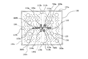
- the millimeter wave circuit shown in FIG. 3 is a transmitter.
- the MMIC 600a functions as a transmission amplifier, and the MMIC 600b functions as a frequency converter.
- terminals 111a and 113a connected to the capacitors 700a and 700b, two terminals 112a and 114a connected to the MMIC 600b, and a terminal 115a connected to the dielectric substrate 500b are provided on the multilayer dielectric substrate 100. It has been. Bonding wires 750 are used as these connection means.
- the terminals 111a and 113a are arranged with the MMIC 600a interposed therebetween, the capacitor 700a is arranged between the terminals 111a and MMIC 600a, and the capacitor 700b is arranged between the terminals 113a and MMIC 600a.
- Terminals 111b, 112b, 113b, 114b, and 115b are connected to the terminals 111a, 113a, 112a, 114a, and 115a via wirings 14a, 140b, and the like on the inner layer of the substrate 100, respectively.
- 114b, 115b are disposed on the outer peripheral edge of the rectangular multilayer dielectric substrate 100.
- the first side 100a intersects with a virtual line connecting the MMIC 600a and the terminal 111a and a virtual line connecting the MMIC 600b and the terminal 112a.
- the terminals 113b and 114b are located on the second side 100b opposite to the first side 100a of the substrate 100.
- the terminal 115b is located on the third side 100c of the four sides of the substrate that intersects the dielectric substrate 500b and the terminal 115a with the imaginary line.
- the multilayer dielectric substrate 100 has through holes 120 through which screws 400 a and 400 b for fixing the cap 300 and the base 200 are passed.
- a hole 110 constituting a part of the waveguide 800 is opened so as to correspond to the end of the dielectric substrate 500a opposite to the side connected to the MMIC 600a. Yes.
- the frequency converter (MMIC 600b) is an image suppression type even harmonic mixer. Therefore, an IF signal having a phase difference of 90 degrees is input from the terminals 112b and 114b on the opposite sides 100a and 100b of the multilayer dielectric substrate 100, and the inner-layer wirings 140a and 140b indicated by dotted lines in FIG. Through 140b, the signal is input to the IF terminal of the MMIC 600b via the terminals 112a and 114a.
- the LO signal is sent from the terminal 115b on the third side 100c of the multilayer dielectric substrate 100 to the terminal 115a via the inner layer wiring, and is input from the terminal 115a to the LO signal terminal of the MMIC 600b.
- power is supplied from the terminals 111b and 113b on the opposite sides 100a and 100b of the multilayer dielectric substrate 100 through the inner layer wiring, the terminals 111a and 113a, and the capacitors 700a and 700b.
- a millimeter wave signal that becomes RF (radio frequency) is connected to an external device such as an antenna through a hole 110 as a part of the waveguide.
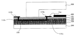
- FIG. 4 is a cross-sectional view showing the structure of the millimeter wave module of this embodiment.
- the multilayer dielectric substrate 100 has a four-layer structure, and the first layer 101 as the surface layer is a Rogers material (RO4350B), and the second layer 102, which is the inner layer of the multilayer substrate, and the second layer
- the 3rd layer 103 and the 4th layer 104 which is a back surface layer are comprised by FR4.
- Such a multilayer substrate is sandwiched between a metal base 200 and a cap 300 so that they cannot be moved by tightening screws 400a and 400b (see also FIG. 2).
- the cap 300 covers the millimeter wave circuit on the multilayer dielectric substrate 100 but exposes the external connection terminals 111b, 112b, 113b, 114b, and 115b disposed on the periphery of the multilayer dielectric substrate 100. Has been.
- the LO signal is input to the mixer MMIC 600 from the outside in the millimeter wave module having such a structure
- the LO signal is input from the peripheral terminal 115b of the multilayer dielectric substrate 100.
- the LO signal is transmitted to the second layer 102 at the interference portion of the cap 300 (the portion where the cap 300 contacts the surface of the multilayer dielectric substrate 100) in order to avoid electrical interference with the metal cap 300. It passes through the formed wiring 150.
- the connection between the terminal pattern of the first layer 101 as the surface layer and the wiring 150 of the second layer 102 is made through the through hole 116b.
- the LO signal is connected from the second layer wiring 150 to the surface layer terminal 115a through the through hole 116a in the vicinity of the MMIC 600, and then connected to the LO terminal of the mixer MMIC 600 by the gold wire 750.
- FIG. 5 shows a state in which the millimeter wave module according to this embodiment is assembled.
- a multilayer dielectric substrate 100 on which components (MMICs 600a and 600b, dielectric substrates 500a and 500b) of millimeter wave circuits are mounted is installed on an aluminum base 200.
- An aluminum cap 300 is placed on the dielectric substrate 100.
- the screws 400a and 400b are passed through the cap 300 and the multilayer dielectric substrate 100 from above the cap 300, and the tips of the screws 400a and 400b are screwed into the base 200, whereby the multilayer dielectric substrate 100 is made of aluminum.
- the structure is sandwiched between the base 200 and the cap 300.
- the MMICs 600 a and 600 b and the dielectric substrates 500 a and 500 b on the multilayer dielectric substrate 100 are accommodated in the cavity 850 of the cap 300, and the peripheral terminals 111 b and 111 b on the multilayer dielectric substrate 100 are disposed outside the cap 300. 112b, 113b, 114b, and 115b are exposed.
- Each screw 400a, 400b is passed through the through hole 120 of the multilayer dielectric substrate 100 shown in FIG.
- a through hole (not shown) is also provided in the cap 300 corresponding to the through hole 120.
- an assembly method in which the screws 400 a and 400 b are threaded into the cap 300 through the base 200 and the multilayer dielectric substrate 100 from below the base 200 may be used.
- the multilayer dielectric substrate 100 is a general substrate composed of a Rogers material and FR4, and is excellent in availability and cost.
- the metal base 200 and the cap 300 are made of aluminum, and are excellent in workability and cost.
- the millimeter wave module having such a configuration is configured by a general multilayer dielectric substrate for electrically connecting the millimeter wave circuit to the outside.
- this structure is sandwiched between a metal base and a cap, and these are held in place with screws.
- the base and cap on which the waveguide is formed can be easily changed in accordance with the frequency band in which the millimeter wave circuit is used.
- Aluminum bases and caps are easy to process and reduce manufacturing costs. In other words, it can be said that the structure can flexibly respond to specification changes to millimeter wave circuits for other frequency bands and is extremely excellent in reducing the cost of millimeter wave modules.
- the composite substrate of the Rogers material and FR4 is used as the multilayer dielectric substrate, but a multilayer substrate of only the Rogers material may be used instead of the composite material.
- the description has been made assuming the even harmonic mixer of the millimeter wave band. For this reason, since the frequency of the LO signal is 1 ⁇ 2 of the RF signal frequency, a designed microstrip line is assumed as the input line of the LO signal from the terminal 115b to the mixer MMIC (FIGS. 2 to 5). 4).
- the present invention is not limited to this, and the LO signal external connection means may be constituted by a waveguide 950 as shown in FIG.
Landscapes
- Transceivers (AREA)
Abstract
La présente invention concerne un module d'ondes millimétriques qui comprend : un circuit d'ondes millimétriques constitué par une pluralité de MMIC (600a, 600b) et de lignes (500a, 500b) de transmission connectant les MMIC ; et un substrat (100) diélectrique multicouche sur lequel est monté le circuit d'ondes millimétriques. Le circuit d'ondes millimétriques est monté sur une couche de surface du substrat (100) diélectrique multicouche. Le module d'ondes millimétriques comprend également : une base (200) métallique destinée à supporter le substrat (100) diélectrique multicouche sur lequel le circuit d'ondes millimétriques est monté ; un chapeau (300) métallique installé sur la couche de surface et recouvrant le circuit d'ondes millimétriques ; et des vis (400a, 400b) qui pénètrent à la fois dans le chapeau (300) et dans le substrat (100) diélectrique multicouche et qui sont vissées dans la base (200). Le substrat (100) diélectrique multicouche est intercalé entre la base (200) et le chapeau (300) au moyen desdites vis.
Priority Applications (1)
| Application Number | Priority Date | Filing Date | Title |
|---|---|---|---|
| JP2015518287A JPWO2014189105A1 (ja) | 2013-05-23 | 2014-05-22 | ミリ波モジュール |
Applications Claiming Priority (2)
| Application Number | Priority Date | Filing Date | Title |
|---|---|---|---|
| JP2013108859 | 2013-05-23 | ||
| JP2013-108859 | 2013-05-23 |
Publications (1)
| Publication Number | Publication Date |
|---|---|
| WO2014189105A1 true WO2014189105A1 (fr) | 2014-11-27 |
Family
ID=51933656
Family Applications (1)
| Application Number | Title | Priority Date | Filing Date |
|---|---|---|---|
| PCT/JP2014/063581 Ceased WO2014189105A1 (fr) | 2013-05-23 | 2014-05-22 | Module d'ondes millimétriques |
Country Status (2)
| Country | Link |
|---|---|
| JP (1) | JPWO2014189105A1 (fr) |
| WO (1) | WO2014189105A1 (fr) |
Cited By (3)
| Publication number | Priority date | Publication date | Assignee | Title |
|---|---|---|---|---|
| JP2015149420A (ja) * | 2014-02-07 | 2015-08-20 | 株式会社東芝 | ミリ波帯用半導体パッケージおよびミリ波帯用半導体装置 |
| JP2017045748A (ja) * | 2015-08-24 | 2017-03-02 | 富士通株式会社 | 高周波用フリップチップ実装用基板、高周波モジュール、及び、高周波モジュールの製造方法 |
| KR101948588B1 (ko) | 2017-12-18 | 2019-02-15 | 한국광기술원 | 밀리미터 웨이브 신호 전송 접속 장치 |
Citations (6)
| Publication number | Priority date | Publication date | Assignee | Title |
|---|---|---|---|---|
| JPH10125830A (ja) * | 1996-10-24 | 1998-05-15 | Hitachi Ltd | 高周波モジュールおよびその製造方法 |
| JP2001177312A (ja) * | 1999-12-15 | 2001-06-29 | Hitachi Kokusai Electric Inc | 高周波接続モジュール |
| US6265774B1 (en) * | 1998-11-19 | 2001-07-24 | Trw Inc. | Millimeter wave adjustable cavity package |
| JP2001358242A (ja) * | 2000-06-16 | 2001-12-26 | Toshiba Corp | マイクロ波パッケージ |
| JP2002164465A (ja) * | 2000-11-28 | 2002-06-07 | Kyocera Corp | 配線基板、配線ボード、それらの実装構造、ならびにマルチチップモジュール |
| JP2009535973A (ja) * | 2006-05-04 | 2009-10-01 | ジョージア テック リサーチ コーポレイション | ミリメートル波のマルチギガビット無線システムのためのモジュール、フィルタおよびアンテナ技術 |
-
2014
- 2014-05-22 WO PCT/JP2014/063581 patent/WO2014189105A1/fr not_active Ceased
- 2014-05-22 JP JP2015518287A patent/JPWO2014189105A1/ja active Pending
Patent Citations (6)
| Publication number | Priority date | Publication date | Assignee | Title |
|---|---|---|---|---|
| JPH10125830A (ja) * | 1996-10-24 | 1998-05-15 | Hitachi Ltd | 高周波モジュールおよびその製造方法 |
| US6265774B1 (en) * | 1998-11-19 | 2001-07-24 | Trw Inc. | Millimeter wave adjustable cavity package |
| JP2001177312A (ja) * | 1999-12-15 | 2001-06-29 | Hitachi Kokusai Electric Inc | 高周波接続モジュール |
| JP2001358242A (ja) * | 2000-06-16 | 2001-12-26 | Toshiba Corp | マイクロ波パッケージ |
| JP2002164465A (ja) * | 2000-11-28 | 2002-06-07 | Kyocera Corp | 配線基板、配線ボード、それらの実装構造、ならびにマルチチップモジュール |
| JP2009535973A (ja) * | 2006-05-04 | 2009-10-01 | ジョージア テック リサーチ コーポレイション | ミリメートル波のマルチギガビット無線システムのためのモジュール、フィルタおよびアンテナ技術 |
Cited By (3)
| Publication number | Priority date | Publication date | Assignee | Title |
|---|---|---|---|---|
| JP2015149420A (ja) * | 2014-02-07 | 2015-08-20 | 株式会社東芝 | ミリ波帯用半導体パッケージおよびミリ波帯用半導体装置 |
| JP2017045748A (ja) * | 2015-08-24 | 2017-03-02 | 富士通株式会社 | 高周波用フリップチップ実装用基板、高周波モジュール、及び、高周波モジュールの製造方法 |
| KR101948588B1 (ko) | 2017-12-18 | 2019-02-15 | 한국광기술원 | 밀리미터 웨이브 신호 전송 접속 장치 |
Also Published As
| Publication number | Publication date |
|---|---|
| JPWO2014189105A1 (ja) | 2017-02-23 |
Similar Documents
| Publication | Publication Date | Title |
|---|---|---|
| KR102266668B1 (ko) | 고주파 모듈 | |
| US10512153B2 (en) | High frequency circuit | |
| US8119922B2 (en) | Dual cavity, high-heat dissipating printed wiring board assembly | |
| US8654542B2 (en) | High-frequency switch module | |
| CN103650132B (zh) | 无线模块 | |
| JP2008244289A (ja) | 電磁シールド構造 | |
| JPWO2010023827A1 (ja) | 導波管、導波管接続構造および導波管接続方法 | |
| CN112885811A (zh) | 多层基板的垂直互连结构 | |
| US11659658B2 (en) | Multilayer board | |
| JP2017187379A (ja) | 多層基板回路モジュール、無線通信装置およびレーダ装置 | |
| KR101555403B1 (ko) | 배선기판 | |
| WO2014189105A1 (fr) | Module d'ondes millimétriques | |
| US9450282B2 (en) | Connection structure between a waveguide and a substrate, where the substrate has an opening larger than a waveguide opening | |
| CN107799489A (zh) | 电子装置 | |
| CN104576616B (zh) | 模块集成电路封装结构及其制作方法 | |
| KR20140073786A (ko) | 마이크로파 송수신모듈 및 이의 패키지 방법 | |
| WO2022215372A1 (fr) | Module de circuit électronique | |
| TW201513295A (zh) | 具有電性屏蔽功能的模組積體電路封裝結構及其製作方法 | |
| JPH09167825A (ja) | 複合マイクロ波集積回路 | |
| US20200083183A1 (en) | Electronic component and electronic device | |
| US12446159B2 (en) | Electronic circuit module | |
| US12622299B2 (en) | Electronic circuit module | |
| US9172126B2 (en) | Module and coupling arrangement | |
| CN219998479U (zh) | 电子器件 | |
| JP2025151075A (ja) | 基板、及び通信デバイス |
Legal Events
| Date | Code | Title | Description |
|---|---|---|---|
| 121 | Ep: the epo has been informed by wipo that ep was designated in this application |
Ref document number: 14800373 Country of ref document: EP Kind code of ref document: A1 |
|
| ENP | Entry into the national phase |
Ref document number: 2015518287 Country of ref document: JP Kind code of ref document: A |
|
| NENP | Non-entry into the national phase |
Ref country code: DE |
|
| 122 | Ep: pct application non-entry in european phase |
Ref document number: 14800373 Country of ref document: EP Kind code of ref document: A1 |