WO2014192518A1 - 露光用光源およびマスクの設計方法、プログラム - Google Patents
露光用光源およびマスクの設計方法、プログラム Download PDFInfo
- Publication number
- WO2014192518A1 WO2014192518A1 PCT/JP2014/062514 JP2014062514W WO2014192518A1 WO 2014192518 A1 WO2014192518 A1 WO 2014192518A1 JP 2014062514 W JP2014062514 W JP 2014062514W WO 2014192518 A1 WO2014192518 A1 WO 2014192518A1
- Authority
- WO
- WIPO (PCT)
- Prior art keywords
- opc
- smo
- pattern
- mask
- restriction rule
- Prior art date
- Legal status (The legal status is an assumption and is not a legal conclusion. Google has not performed a legal analysis and makes no representation as to the accuracy of the status listed.)
- Ceased
Links
Images


Classifications
-
- G—PHYSICS
- G03—PHOTOGRAPHY; CINEMATOGRAPHY; ANALOGOUS TECHNIQUES USING WAVES OTHER THAN OPTICAL WAVES; ELECTROGRAPHY; HOLOGRAPHY
- G03F—PHOTOMECHANICAL PRODUCTION OF TEXTURED OR PATTERNED SURFACES, e.g. FOR PRINTING, FOR PROCESSING OF SEMICONDUCTOR DEVICES; MATERIALS THEREFOR; ORIGINALS THEREFOR; APPARATUS SPECIALLY ADAPTED THEREFOR
- G03F1/00—Originals for photomechanical production of textured or patterned surfaces, e.g., masks, photo-masks, reticles; Mask blanks or pellicles therefor; Containers specially adapted therefor; Preparation thereof
- G03F1/36—Masks having proximity correction features; Preparation thereof, e.g. optical proximity correction [OPC] design processes
-
- G—PHYSICS
- G03—PHOTOGRAPHY; CINEMATOGRAPHY; ANALOGOUS TECHNIQUES USING WAVES OTHER THAN OPTICAL WAVES; ELECTROGRAPHY; HOLOGRAPHY
- G03F—PHOTOMECHANICAL PRODUCTION OF TEXTURED OR PATTERNED SURFACES, e.g. FOR PRINTING, FOR PROCESSING OF SEMICONDUCTOR DEVICES; MATERIALS THEREFOR; ORIGINALS THEREFOR; APPARATUS SPECIALLY ADAPTED THEREFOR
- G03F1/00—Originals for photomechanical production of textured or patterned surfaces, e.g., masks, photo-masks, reticles; Mask blanks or pellicles therefor; Containers specially adapted therefor; Preparation thereof
- G03F1/68—Preparation processes not covered by groups G03F1/20 - G03F1/50
- G03F1/70—Adapting basic layout or design of masks to lithographic process requirements, e.g., second iteration correction of mask patterns for imaging
-
- G—PHYSICS
- G06—COMPUTING OR CALCULATING; COUNTING
- G06F—ELECTRIC DIGITAL DATA PROCESSING
- G06F30/00—Computer-aided design [CAD]
- G06F30/30—Circuit design
- G06F30/39—Circuit design at the physical level
- G06F30/392—Floor-planning or layout, e.g. partitioning or placement
-
- G—PHYSICS
- G03—PHOTOGRAPHY; CINEMATOGRAPHY; ANALOGOUS TECHNIQUES USING WAVES OTHER THAN OPTICAL WAVES; ELECTROGRAPHY; HOLOGRAPHY
- G03F—PHOTOMECHANICAL PRODUCTION OF TEXTURED OR PATTERNED SURFACES, e.g. FOR PRINTING, FOR PROCESSING OF SEMICONDUCTOR DEVICES; MATERIALS THEREFOR; ORIGINALS THEREFOR; APPARATUS SPECIALLY ADAPTED THEREFOR
- G03F7/00—Photomechanical, e.g. photolithographic, production of textured or patterned surfaces, e.g. printing surfaces; Materials therefor, e.g. comprising photoresists; Apparatus specially adapted therefor
- G03F7/70—Microphotolithographic exposure; Apparatus therefor
- G03F7/70425—Imaging strategies, e.g. for increasing throughput or resolution, printing product fields larger than the image field or compensating lithography- or non-lithography errors, e.g. proximity correction, mix-and-match, stitching or double patterning
- G03F7/70433—Layout for increasing efficiency or for compensating imaging errors, e.g. layout of exposure fields for reducing focus errors; Use of mask features for increasing efficiency or for compensating imaging errors
- G03F7/70441—Optical proximity correction [OPC]
-
- G—PHYSICS
- G03—PHOTOGRAPHY; CINEMATOGRAPHY; ANALOGOUS TECHNIQUES USING WAVES OTHER THAN OPTICAL WAVES; ELECTROGRAPHY; HOLOGRAPHY
- G03F—PHOTOMECHANICAL PRODUCTION OF TEXTURED OR PATTERNED SURFACES, e.g. FOR PRINTING, FOR PROCESSING OF SEMICONDUCTOR DEVICES; MATERIALS THEREFOR; ORIGINALS THEREFOR; APPARATUS SPECIALLY ADAPTED THEREFOR
- G03F7/00—Photomechanical, e.g. photolithographic, production of textured or patterned surfaces, e.g. printing surfaces; Materials therefor, e.g. comprising photoresists; Apparatus specially adapted therefor
- G03F7/70—Microphotolithographic exposure; Apparatus therefor
- G03F7/70483—Information management; Active and passive control; Testing; Wafer monitoring, e.g. pattern monitoring
- G03F7/70491—Information management, e.g. software; Active and passive control, e.g. details of controlling exposure processes or exposure tool monitoring processes
- G03F7/705—Modelling or simulating from physical phenomena up to complete wafer processes or whole workflow in wafer productions
-
- G—PHYSICS
- G06—COMPUTING OR CALCULATING; COUNTING
- G06F—ELECTRIC DIGITAL DATA PROCESSING
- G06F30/00—Computer-aided design [CAD]
- G06F30/30—Circuit design
- G06F30/39—Circuit design at the physical level
Definitions
- the present invention relates to an exposure light source and mask design method and program, and more specifically, an exposure light source and mask design method and program using source mask optimization (SMO) and optical proximity correction (OPC). About.
- SMO source mask optimization
- OPC optical proximity correction
- OPC optical proximity correction
- the source (light source) mask optimization method (hereinafter referred to as SMO)
- SMO source mask optimization method
- Patent Document 1 and Non-Patent Document 1 disclose an exposure mask optimization method using OPC and SMO. In that method, first, SMO is performed on a selected pattern to obtain an optimized light source, and then, using a light source optimized by SMO, OPC, etc., to fit a full chip. Design the mask shape.
- SMO and OPC are separately performed and individually optimized, so that the final mask is not necessarily combined with the advantages of both.
- Pattern optimization is not always performed.
- the light source shape optimized by SMO may not be optimal for OPC.
- the light source and the mask are not optimized so that the cooperative relationship between SMO and OPC is sufficiently exhibited or appropriately used.
- the presence / absence and optimization of the cooperative relationship between the so-called hot spot area including the dense / complex pattern and the other area are not performed.
- the object of the present invention is not performed by the conventional exposure light source and mask optimization method using OPC and SMO, and the optimal relationship between the two is fully utilized or the mask pattern is properly used appropriately. It is to provide a design (design) method.
- the present invention provides a method for designing an exposure light source and a mask.
- the method includes a step of selecting a predetermined pattern group and a step of performing SMO using the predetermined pattern group, wherein the shift of the polygon edge position when applying OPC to the predetermined pattern group is performed.
- a step of performing SMO under a selectively restricted OPC restriction rule and a light source optimized by the SMO are used to determine the layout of the exposure mask by applying OPC to the entire pattern of the exposure mask. Steps.
- the light source by SMO is reflected while reflecting the correction effect by OPC and improving the efficiency of SMO calculation. Can be optimized.
- the step of performing SMO performs SMO on at least some selected patterns in the pattern group under an OPC restriction rule, and applies to patterns other than some patterns in the pattern group. Performing SMO without using OPC restriction rules.
- the step of performing the SMO that does not use the OPC restriction rule is performed for a pattern in which the SMO calculation result cannot be obtained within a predetermined time.
- the OPC restriction rule includes fixing at least some selected edges among polygon edges of a predetermined pattern group and fixing edges of sub-resolution assist features (SRAF). At least some of the edges include edges defined by OPC performed after the SMO is performed, or include edges that are shorter than a predetermined length.
- SRAF sub-resolution assist features
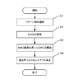
- FIG. 1 is a diagram showing a flow of an exposure mask design method of the present invention.
- the flow in FIG. 1 is implemented by a computer executing a program (software) for the method.
- a pattern group is selected. It is not practical to apply SMO to the entire chip, in other words, the entire mask layout due to the large amount of calculation. Therefore, it is necessary to select a pattern group necessary for performing SMO first.
- the selection of the pattern group is performed so as to include a portion of a high-density pattern with a small (strict) tolerance of pattern deviation in the chip. For example, a pattern forming an SRAM or the like, a so-called hot spot is selected.
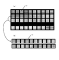
- FIG. 2 is an image diagram of pattern group selection. More precisely, the pattern group is selected as a clip indicated by reference numeral 10 in FIG. In FIG. 2, each white pattern area in the black frame represents a clip. A clip typically represents a small part of a design (ie, circuit, cell, or pattern) that requires specific verification. As shown in FIG. 2A, the necessary number and type of clips are selected from a library including a set of clips. FIG. 2B illustrates the selection of 10 clips 10 as an example of selection. For example, about 100 to 1000 clips are selected as necessary.
- step S2 SMO is performed using the pattern (clip) group selected in step S1.
- the SMO of the present invention is roughly divided into two features.
- the first feature is SMO calculation, that is, under non-linear programming for SMO (hereinafter referred to as NLP), calculated under an OPC restriction rule that selectively restricts the shift of polygon edge positions when OPC is applied. Is to do.
- the second feature is to change the SMO embodiment including whether to apply the OPC restriction rule selectively to the pattern (clip) group including the SMO embodiment under the OPC restriction rule. That is.
- NLP non-linear programming for SMO
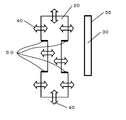
- FIG. 3 is a diagram for explaining a shift constraint on polygon edge positions according to an embodiment of the present invention.
- reference numeral 20 indicates a polygon for OPC corresponding to a pattern (clip)
- reference numeral 30 indicates a sub-resolution assist feature (hereinafter referred to as SRAF) arranged in the OPC.
- SRAF sub-resolution assist feature
- the polygon edge position shift constraint used in this specification includes not only the polygon 20 but also the SRAF 30 as illustrated in FIG. 3 that is generally rectangular, and includes these edge position shift constraints. Sometimes used in a broad sense.
- all the edges (sides) of the polygon 20 can be freely shifted in the NLP calculation.
- restrictions are imposed on the shift of the edge (side) of the conventional polygon 20.
- a predetermined edge shift as exemplified by the edge (side) 50 of the polygon 20 in FIG. 3 is limited, and the edge 50 is fixed.
- the predetermined edge mentioned here is an edge defined to be fixed in step S3 in FIG. Or it is good also as an edge which fixes a short edge below predetermined length (for example, 10 nm).
- the edge 55 that defines the shape of the SRAF 30 is fixed so that the shape (line width) of the SRAF 30 cannot be varied.
- the NLP solution is performed by obtaining a minimum value (minf (x)) of a conventional objective function f (x) under a predetermined constraint condition.
- the objective function f (x) includes, for example, a process window related to parameters (performance) such as lithography manufacturability verification (hereinafter referred to as LMC), a process availability band (hereinafter referred to as PV band), and the like. It is.
- LMC lithography manufacturability verification
- PV band process availability band
- EPE edge placement error
- variable x is a value indicating the pixel value of the light source and the mask shape.
- the amplitude of each frequency component obtained by Fourier transform of the mask shape is set as the variable x.
- the mask shape is expressed in the spatial domain, the position of each edge of the polygon is set as the variable x.
- the predetermined constraint conditions include, for example, lithography constraints (settings) such as a mask error increase coefficient (hereinafter referred to as MEEF) and contrast.
- MEEF mask error increase coefficient
- edge shift restriction that is, the degree of freedom of variable x is small Therefore, depending on the pattern (clip), there may occur a case where the minimum value of the objective function f (x) cannot be obtained (not converged) within a predetermined time in the NLP.
- the OPC restriction rule is not applied, and instead, the mask shape in the spatial region with the polygon edge position as a variable is Fourier-transformed. SMO is performed using the mask shape in the frequency domain.
- a mask in the frequency domain after the Fourier transform described above without applying the OPC restriction rule to a pattern (clip) specified in advance for example, a pattern (clip) corresponding to a hot spot.
- a pattern (clip) corresponding to a hot spot It is also possible to implement the SMO by applying the OPC restriction rule described above to other patterns (clips) using the shape.
- wavefront engineering hereinafter referred to as WE
- WE wavefront engineering
- application of WE means conversion from a mask shape expressed in the frequency domain to a mask shape expressed in the spatial domain.
- OPC is applied to patterns (clips) converted to mask shapes expressed in the spatial domain by WE and patterns (clips) handled as mask shapes expressed in the frequency domain to which WE is not applied.
- a light source considering OPC can be obtained, and at the same time, an optimized final mask shape can be obtained without applying an OPC restriction rule to a pattern (clip) corresponding to a hot spot. .
- the SMO that is appropriate for the pattern (clip) is performed while avoiding the overflow of the SMO processing. It becomes possible.
- the mask shape data obtained by applying the OPC restriction rule among the mask shape data obtained as a result of the SMO implementation in step S2 in FIG. 1 is discarded, and the mask shape obtained by the OPC implementation in step S3 is determined. Used.
- the mask shape data obtained by applying WE without applying the OPC restriction rule in the SMO implementation in step S2 is replaced with the mask shape obtained by the OPC implementation in the next OPC implementation in step S3. Used.
- step S3 OPC is performed on the entire mask layout of the chip using the SMO result obtained in step S2. Specifically, using the optimum light source obtained in step S2, OPC is performed on each pattern in the mask layout to obtain optimum mask pattern data. At this time, as described above, the mask shape data obtained by applying WE without applying the OPC restriction rule is used as it is by replacing the mask shape obtained by performing OPC.
- step S4 the layout of the exposure mask (reticle) is determined / created using the mask pattern data obtained as the OPC result of step S3.
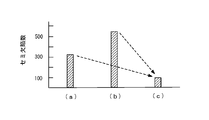
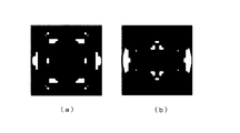
- FIGS. 4A to 4C are image diagrams of light sources obtained by the respective SMO processes (a) to (c).
- a bright (white) portion in each figure indicates a light emitting area (pixel).
- OPC is performed on all 100 clips using the light sources shown in FIGS. 4A to 4C, and in the pattern layout obtained from the OPC results, semi (half) defects are detected. Counted the number.
- the semi (semi) defect is not a complete defect such as when the patterns are connected (short) (bridge), or the pattern is broken (pinch), but it is a complete defect. This means a state of a pattern in which PV bands that are likely to reach are close to each other within a predetermined interval.
- FIG. 5 shows the number of semi (half) defects corresponding to each of the above (a) to (c).
- the number of semi (half) defects when using the SMO implementation under the OPC restriction rule of the present invention of FIG. 5 (c) is the mask shape in the conventional frequency domain and spatial domain of (a) and (b). This is significantly smaller than the number of semi-defects in the case of using SMO when S is used.
- FIGS. 6A and 6 (b) are image diagrams of the respective light sources obtained by the SMO processing of (a) and (b) above. A bright (white) portion in each figure indicates a light emitting area (pixel).
- OPC is performed on all 100 clips using the light sources shown in FIGS. 6A and 6B, and in the pattern layout obtained from the OPC results, semi (half) defects are detected. Counted the number.
- FIG. 7 shows the number of semi (half) defects corresponding to each of the above (a) and (b).
- the number of semi (semi) defects when the selective SMO implementation of the present invention of FIG. 7B is used is the same as that in the case of using the mask shape in the conventional frequency domain of FIG. This is a significant decrease from the number of semi-defects.
Landscapes
- Physics & Mathematics (AREA)
- General Physics & Mathematics (AREA)
- Engineering & Computer Science (AREA)
- Computer Hardware Design (AREA)
- Theoretical Computer Science (AREA)
- Architecture (AREA)
- Evolutionary Computation (AREA)
- Geometry (AREA)
- General Engineering & Computer Science (AREA)
- Preparing Plates And Mask In Photomechanical Process (AREA)
- Exposure And Positioning Against Photoresist Photosensitive Materials (AREA)
Abstract
Description
図3は、本発明の一実施形態のポリゴンのエッジ位置のシフト制約を説明するための図である。図3において、符号20は、パターン(クリップ)に対応したOPCのためのポリゴンを示し、符号30は、OPCにおいて配置されるサブ解像度アシストフィーチャ(以下、SRAFと呼ぶ)を示している。なお、本明細書中で用いるポリゴンのエッジ位置のシフト制約は、ポリゴン20のみならず、一般に長方形をなす図3に例示されるようなSRAF30をも含めて、これらのエッジ位置のシフト制約を含む広い意味で用いる場合がある。
(A)で説明したOPC制限ルール下で、NLPを解いてSMOをおこなう場合、エッジシフトの制約がある、すなわち変数xの自由度が小さいので、パターン(クリップ)によっては、NLPにおいて所定の時間内に目的関数f(x)の最小値を求めることができない(収束しない)場合が起こり得る。その場合は、解が得られないパターン(クリップ)に対しては、OPC制限ルールを適用せずに、代わりに、ポリゴンのエッジ位置を変数とする空間領域におけるマスク形状をフーリエ変換して得られる周波数領域におけるマスク形状を用いてSMOを実施する。すなわち、複数あるパターン(クリップ)のうち、一部は空間領域におけるマスク形状として扱ってOPC制限ルールを適用し、残りのパターン(クリップ)については周波数空間におけるマスク形状として扱ってOPC制限ルールを適用せず、空間領域におけるマスク形状と周波数領域におけるマスク形状とを混合した状態で同時最適化のSMOを実施する。
(a)従来の周波数を変数とする周波数領域におけるマスク形状を用いたSMOの実施
(b)従来のポリゴンのエッジ位置を変数とする空間領域におけるマスク形状を用いたSMOの実施
(c)上述した本発明の実施形態であるポリゴンのエッジ位置を変数とする空間領域におけるマスク形状を用い、OPC制限ルールを適用したSMOの実施
(a)8クリップの全てに対して従来の周波数を変数とする周波数領域におけるマスク形状を用いたSMOの実施
(b)8クリップ中の3クリップに対して周波数を変数とする周波数領域におけるマスク形状を用い、残る5クリップに対してポリゴンのエッジ位置を変数とする空間領域におけるマスク形状を用い、本発明のOPC制限ルールを適用したSMOの実施
20 ポリゴン
30 SRAF
50、55 固定エッジ
Claims (16)
- 露光用光源およびマスクを設計する方法であって、
所定のパターン群を選択するステップと、
前記パターン群を用いて光源マスク最適化(SMO)を実施するステップであって、前記パターン群に対して光近接効果補正(OPC)を適用する際のポリゴンのエッジ位置のシフトを選択的に制限したOPC制限ルール下でSMOを実施するステップと、
SMOにより最適化された光源を用いて、露光用マスクのパターン全体に対してOPCを適用して前記露光用マスクのレイアウトを決定するステップと、
を含む、方法。 - 前記SMOを実施するステップは、
前記パターン群の選択された少なくとも一部のパターンに対して前記OPC制限ルール下でSMOを実施するステップと、
前記パターン群の前記一部のパターン以外のパターンに対して前記OPC制限ルールを用いないOPCを適用してSMOを実施するステップと、
を含む、請求項1に記載の方法。 - 前記OPC制限ルールを用いないOPCを適用してSMOを実施するステップは、所定の時間内にSMOの計算結果が得られないパターンに対して実施される、請求項2に記載の方法。
- 前記OPC制限ルールを用いないOPCを適用してSMOを実施するステップは、前記ポリゴンのエッジ位置を変数とする空間領域におけるマスク形状をフーリエ変換して得られる周波数領域におけるマスク形状を用いてSMOを実施することを含む、請求項2に記載の方法。
- 前記少なくとも一部のパターンは、ホットスポットに対応したパターンを含む、請求項2に記載の方法。
- 前記OPC制限ルールは、前記パターン群のポリゴンのエッジ中の選択された少なくとも一部のエッジの固定と、サブ解像度アシストフィーチャ(SRAF)のエッジの固定とを含む、請求項1~5のいずれか1項に記載の方法。
- 前記少なくとも一部のエッジは、前記SMOの実施後に行うOPCで定義されるエッジを含む、請求項6に記載の方法。
- 前記少なくとも一部のエッジは、所定の長さよりも短いエッジを含む、請求項6に記載の方法。
- 露光用光源およびマスクを設計するためのコンピュータ・プログラムであって、コンピュータに、
所定のパターン群を選択するステップと、
前記パターン群を用いて光源マスク最適化(SMO)を実施するステップであって、前記パターン群に対して光近接効果補正(OPC)を適用する際のポリゴンのエッジ位置のシフトを選択的に制限したOPC制限ルール下でSMOを実施するステップと、
SMOにより最適化された光源を用いて、露光用マスクのパターン全体に対してOPCを適用して前記露光用マスクのレイアウトを決定するステップと、を実行させることを含む、コンピュータ・プログラム。 - 前記SMOを実施するステップは、
前記パターン群の選択された少なくとも一部のパターンに対して前記OPC制限ルール下でのSMOを実施するステップと、
前記パターン群の前記一部のパターン以外のパターンに対して前記OPC制限ルールを用いないOPCを適用してSMOを実施するステップと、
を含む、請求項9に記載のコンピュータ・プログラム。 - 前記OPC制限ルールを用いないOPCを適用してSMOを実施するステップは、所定の時間内にSMOの計算結果が得られないパターンに対して実施される、請求項10に記載のコンピュータ・プログラム。
- 前記OPC制限ルールを用いないOPCを適用してSMOを実施するステップは、前記ポリゴンのエッジ位置を変数とする空間領域におけるマスク形状をフーリエ変換して得られる周波数領域におけるマスク形状を用いてSMOを実施することを含む、請求項10に記載のコンピュータ・プログラム。
- 前記少なくとも一部のパターンは、ホットスポットに対応したパターンを含む、請求項10に記載のコンピュータ・プログラム。
- 前記OPC制限ルールは、前記パターン群に対するポリゴンのエッジ中の選択された少なくとも一部のエッジの固定と、サブ解像度アシストフィーチャ(SRAF)のエッジの固定とを含む、請求項9~13に記載のコンピュータ・プログラム。
- 前記少なくとも一部のエッジは、前記SMOの実施後に行うOPCで定義されるエッジを含む、請求項14に記載のコンピュータ・プログラム。
- 前記少なくとも一部のエッジは、所定の長さよりも短いエッジを含む、請求項14に記載のコンピュータ・プログラム。
Priority Applications (2)
| Application Number | Priority Date | Filing Date | Title |
|---|---|---|---|
| DE112014000486.3T DE112014000486B4 (de) | 2013-05-27 | 2014-05-09 | Verfahren und Programmprodukt zum Entwerfen einer Quelle und einer Maske für die Lithographie |
| US14/892,987 US9857676B2 (en) | 2013-05-27 | 2014-05-09 | Method and program product for designing source and mask for lithography |
Applications Claiming Priority (2)
| Application Number | Priority Date | Filing Date | Title |
|---|---|---|---|
| JP2013-110534 | 2013-05-27 | ||
| JP2013110534 | 2013-05-27 |
Publications (1)
| Publication Number | Publication Date |
|---|---|
| WO2014192518A1 true WO2014192518A1 (ja) | 2014-12-04 |
Family
ID=51988556
Family Applications (1)
| Application Number | Title | Priority Date | Filing Date |
|---|---|---|---|
| PCT/JP2014/062514 Ceased WO2014192518A1 (ja) | 2013-05-27 | 2014-05-09 | 露光用光源およびマスクの設計方法、プログラム |
Country Status (3)
| Country | Link |
|---|---|
| US (1) | US9857676B2 (ja) |
| DE (1) | DE112014000486B4 (ja) |
| WO (1) | WO2014192518A1 (ja) |
Cited By (2)
| Publication number | Priority date | Publication date | Assignee | Title |
|---|---|---|---|---|
| CN104914684A (zh) * | 2015-06-24 | 2015-09-16 | 北京理工大学 | 一种极紫外光刻光源-掩模联合优化方法 |
| CN111781804A (zh) * | 2020-07-16 | 2020-10-16 | 中国科学院上海光学精密机械研究所 | 基于协方差矩阵自适应进化策略算法的光源掩模优化方法 |
Families Citing this family (2)
| Publication number | Priority date | Publication date | Assignee | Title |
|---|---|---|---|---|
| CN115616852B (zh) * | 2022-07-27 | 2025-09-02 | 上海华力集成电路制造有限公司 | 改善光刻图形与掩模版上图形的偏差的方法 |
| CN120255260B (zh) * | 2025-03-19 | 2026-01-30 | 西安电子科技大学广州研究院 | 一种用于光刻掩膜校正的多尺度信息融合方法 |
Citations (5)
| Publication number | Priority date | Publication date | Assignee | Title |
|---|---|---|---|---|
| JP2003203849A (ja) * | 2002-01-08 | 2003-07-18 | Mitsubishi Electric Corp | リソグラフィプロセスマージン評価装置、リソグラフィプロセスマージン評価方法およびリソグラフィプロセスマージン評価プログラム |
| JP2013509604A (ja) * | 2009-10-28 | 2013-03-14 | エーエスエムエル ネザーランズ ビー.ブイ. | 光源及びマスクの最適化のためのパターン選択方法 |
| JP2013065018A (ja) * | 2011-09-16 | 2013-04-11 | Imec | 光学リソグラフィでの照明光源形状定義 |
| JP2013165271A (ja) * | 2012-02-09 | 2013-08-22 | Asml Netherlands Bv | 先進リソグラフィのためのレンズ加熱感知ソースマスク最適化 |
| WO2014042044A1 (ja) * | 2012-09-11 | 2014-03-20 | 株式会社ニコン | 瞳輝度分布の設定方法 |
Family Cites Families (32)
| Publication number | Priority date | Publication date | Assignee | Title |
|---|---|---|---|---|
| JPH08297692A (ja) | 1994-09-16 | 1996-11-12 | Mitsubishi Electric Corp | 光近接補正装置及び方法並びにパタン形成方法 |
| US5680588A (en) | 1995-06-06 | 1997-10-21 | International Business Machines Corporation | Method and system for optimizing illumination in an optical photolithography projection imaging system |
| JP4590146B2 (ja) | 2000-02-14 | 2010-12-01 | エーエスエムエル マスクツールズ ビー.ブイ. | フォトマスクの幾何形状を改良する方法 |
| JP2001230250A (ja) | 2000-02-14 | 2001-08-24 | Hitachi Ltd | 半導体装置およびその製造方法並びにマスクパターンの生成方法 |
| JP3615182B2 (ja) | 2001-11-26 | 2005-01-26 | 株式会社東芝 | 光近接効果補正方法及び光近接効果補正システム |
| SG139530A1 (en) | 2003-01-14 | 2008-02-29 | Asml Masktools Bv | Method of optical proximity correction design for contact hole mask |
| US7147975B2 (en) | 2003-02-17 | 2006-12-12 | Matsushita Electric Industrial Co., Ltd. | Photomask |
| JP4009301B2 (ja) | 2003-02-17 | 2007-11-14 | 松下電器産業株式会社 | マスクデータ作成方法 |
| US7355673B2 (en) | 2003-06-30 | 2008-04-08 | Asml Masktools B.V. | Method, program product and apparatus of simultaneous optimization for NA-Sigma exposure settings and scattering bars OPC using a device layout |
| JP2005086119A (ja) | 2003-09-11 | 2005-03-31 | Matsushita Electric Ind Co Ltd | 微細パターンの形成方法 |
| JP4488727B2 (ja) | 2003-12-17 | 2010-06-23 | 株式会社東芝 | 設計レイアウト作成方法、設計レイアウト作成システム、マスクの製造方法、半導体装置の製造方法、及び設計レイアウト作成プログラム |
| US7506299B2 (en) | 2003-12-19 | 2009-03-17 | Asml Holding N.V. | Feature optimization using interference mapping lithography |
| US7269817B2 (en) * | 2004-02-10 | 2007-09-11 | International Business Machines Corporation | Lithographic process window optimization under complex constraints on edge placement |
| JP4050283B2 (ja) | 2005-02-18 | 2008-02-20 | 松下電器産業株式会社 | パターン形成方法 |
| JP2010054710A (ja) | 2008-08-27 | 2010-03-11 | Toshiba Corp | フォトマスク及び半導体装置の製造方法 |
| WO2010059954A2 (en) * | 2008-11-21 | 2010-05-27 | Brion Technologies Inc. | Fast freeform source and mask co-optimization method |
| US8015511B2 (en) | 2009-01-05 | 2011-09-06 | International Business Machines Corporation | Adjustment of mask shapes for improving printability of dense integrated circuit layout |
| JP5607348B2 (ja) | 2009-01-19 | 2014-10-15 | キヤノン株式会社 | 原版データを生成する方法およびプログラム、ならびに、原版製作方法 |
| US8479125B2 (en) * | 2009-03-31 | 2013-07-02 | Christophe Pierrat | Lithography modeling and applications |
| US20110047519A1 (en) * | 2009-05-11 | 2011-02-24 | Juan Andres Torres Robles | Layout Content Analysis for Source Mask Optimization Acceleration |
| US8146025B2 (en) | 2009-07-30 | 2012-03-27 | United Microelectronics Corp. | Method for correcting layout pattern using rule checking rectangle |
| NL2006091A (en) * | 2010-03-05 | 2011-09-06 | Asml Netherlands Bv | Design rule optimization in lithographic imaging based on correlation of functions representing mask and predefined optical conditions. |
| US8402399B2 (en) * | 2010-04-30 | 2013-03-19 | International Business Machines Corporation | Method and system for computing fourier series coefficients for mask layouts using FFT |
| US8667427B2 (en) * | 2011-02-24 | 2014-03-04 | International Business Machines Corporation | Method of optimization of a manufacturing process of an integrated circuit layout |
| US8607170B2 (en) * | 2011-03-02 | 2013-12-10 | Texas Instruments Incorporated | Perturbational technique for co-optimizing design rules and illumination conditions for lithography process |
| US9034542B2 (en) * | 2011-06-25 | 2015-05-19 | D2S, Inc. | Method and system for forming patterns with charged particle beam lithography |
| US8473878B2 (en) * | 2011-11-28 | 2013-06-25 | Synopsys, Inc. | Lithographically enhanced edge determination |
| US9250535B2 (en) * | 2013-03-15 | 2016-02-02 | International Business Machines Corporation | Source, target and mask optimization by incorporating countour based assessments and integration over process variations |
| KR20160084437A (ko) * | 2013-11-08 | 2016-07-13 | 에이에스엠엘 네델란즈 비.브이. | 지향성 자가조립을 위해 가이딩 템플릿을 생성하는 방법론 |
| KR102227127B1 (ko) * | 2014-02-12 | 2021-03-12 | 삼성전자주식회사 | 리소그래피 시뮬레이션을 이용한 디자인룰 생성 장치 및 방법 |
| KR102006321B1 (ko) * | 2014-04-14 | 2019-08-01 | 에이에스엠엘 네델란즈 비.브이. | 리소그래피 공정들에 대한 최적화의 흐름들 |
| US9262820B2 (en) * | 2014-05-19 | 2016-02-16 | United Microelectronics Corporation | Method and apparatus for integrated circuit design |
-
2014
- 2014-05-09 WO PCT/JP2014/062514 patent/WO2014192518A1/ja not_active Ceased
- 2014-05-09 US US14/892,987 patent/US9857676B2/en active Active
- 2014-05-09 DE DE112014000486.3T patent/DE112014000486B4/de active Active
Patent Citations (5)
| Publication number | Priority date | Publication date | Assignee | Title |
|---|---|---|---|---|
| JP2003203849A (ja) * | 2002-01-08 | 2003-07-18 | Mitsubishi Electric Corp | リソグラフィプロセスマージン評価装置、リソグラフィプロセスマージン評価方法およびリソグラフィプロセスマージン評価プログラム |
| JP2013509604A (ja) * | 2009-10-28 | 2013-03-14 | エーエスエムエル ネザーランズ ビー.ブイ. | 光源及びマスクの最適化のためのパターン選択方法 |
| JP2013065018A (ja) * | 2011-09-16 | 2013-04-11 | Imec | 光学リソグラフィでの照明光源形状定義 |
| JP2013165271A (ja) * | 2012-02-09 | 2013-08-22 | Asml Netherlands Bv | 先進リソグラフィのためのレンズ加熱感知ソースマスク最適化 |
| WO2014042044A1 (ja) * | 2012-09-11 | 2014-03-20 | 株式会社ニコン | 瞳輝度分布の設定方法 |
Cited By (3)
| Publication number | Priority date | Publication date | Assignee | Title |
|---|---|---|---|---|
| CN104914684A (zh) * | 2015-06-24 | 2015-09-16 | 北京理工大学 | 一种极紫外光刻光源-掩模联合优化方法 |
| CN111781804A (zh) * | 2020-07-16 | 2020-10-16 | 中国科学院上海光学精密机械研究所 | 基于协方差矩阵自适应进化策略算法的光源掩模优化方法 |
| CN111781804B (zh) * | 2020-07-16 | 2021-07-27 | 中国科学院上海光学精密机械研究所 | 基于协方差矩阵自适应进化策略算法的光源掩模优化方法 |
Also Published As
| Publication number | Publication date |
|---|---|
| US9857676B2 (en) | 2018-01-02 |
| US20160103389A1 (en) | 2016-04-14 |
| DE112014000486B4 (de) | 2021-08-19 |
| DE112014000486T5 (de) | 2015-11-05 |
Similar Documents
| Publication | Publication Date | Title |
|---|---|---|
| US6523165B2 (en) | Alternating phase shift mask design conflict resolution | |
| US8589830B2 (en) | Method and apparatus for enhanced optical proximity correction | |
| US9465906B2 (en) | System and method for integrated circuit manufacturing | |
| TWI806863B (zh) | 為了目標特徵而用於產生包含子解析度輔助特徵的一光罩的方法 | |
| US8234596B2 (en) | Pattern data creating method, pattern data creating program, and semiconductor device manufacturing method | |
| JP2005037945A (ja) | 交番位相シフト・マスク・リソグラフィのマスク・パターンの生成 | |
| US8365106B2 (en) | Method for optimization of light effective source while target pattern is changed | |
| TW201407264A (zh) | 用於光罩製作之積體電路設計方法 | |
| TW201447476A (zh) | 遮罩圖案產生方法,記錄媒介,及資訊處理裝置 | |
| CN105093810B (zh) | 降低关键尺寸的光学邻近修正的边缘定位误差的方法 | |
| WO2014192518A1 (ja) | 露光用光源およびマスクの設計方法、プログラム | |
| US8910098B1 (en) | Neighbor-aware edge fragment adjustment for optical proximity correction | |
| US7730445B2 (en) | Pattern data verification method for semiconductor device, computer-readable recording medium having pattern data verification program for semiconductor device recorded, and semiconductor device manufacturing method | |
| US12505272B2 (en) | Region based shrinking methodology for integrated circuit layout migration | |
| US9465907B2 (en) | Multi-polygon constraint decomposition techniques for use in double patterning applications | |
| CN102681361A (zh) | 光刻仿真的方法及装置 | |
| JP2006292941A (ja) | 光近接効果補正方法およびその装置 | |
| Melville et al. | Demonstrating the benefits of source-mask optimization and enabling technologies through experiment and simulations | |
| JP5663080B2 (ja) | 半導体デバイス設計用のマスク・データの波面処理 | |
| CN115113477A (zh) | 利用有利区域和不利区域的几何掩模规则检查 | |
| Su et al. | SRAF rule extraction and insertion based on inverse lithography technology | |
| CN119291985A (zh) | 一种降低光学邻近效应修正时间的方法 | |
| CN118246390A (zh) | 线图形、沟槽层版图的sraf设计方法 | |
| CN117331288A (zh) | 对线栅图形进行双重图形成像的修正方法及光刻方法 | |
| CN111025856B (zh) | 一种确定光刻工艺节点禁止周期的方法及仿真方法 |
Legal Events
| Date | Code | Title | Description |
|---|---|---|---|
| 121 | Ep: the epo has been informed by wipo that ep was designated in this application |
Ref document number: 14803661 Country of ref document: EP Kind code of ref document: A1 |
|
| WWE | Wipo information: entry into national phase |
Ref document number: 1120140004863 Country of ref document: DE Ref document number: 112014000486 Country of ref document: DE |
|
| WWE | Wipo information: entry into national phase |
Ref document number: 14892987 Country of ref document: US |
|
| 122 | Ep: pct application non-entry in european phase |
Ref document number: 14803661 Country of ref document: EP Kind code of ref document: A1 |