WO2014196043A1 - Module optique et son procédé de fabrication - Google Patents
Module optique et son procédé de fabrication Download PDFInfo
- Publication number
- WO2014196043A1 WO2014196043A1 PCT/JP2013/065632 JP2013065632W WO2014196043A1 WO 2014196043 A1 WO2014196043 A1 WO 2014196043A1 JP 2013065632 W JP2013065632 W JP 2013065632W WO 2014196043 A1 WO2014196043 A1 WO 2014196043A1
- Authority
- WO
- WIPO (PCT)
- Prior art keywords
- optical module
- fiber block
- optical
- protrusion
- adhesive
- Prior art date
- Legal status (The legal status is an assumption and is not a legal conclusion. Google has not performed a legal analysis and makes no representation as to the accuracy of the status listed.)
- Ceased
Links
Images


Classifications
-
- G—PHYSICS
- G02—OPTICS
- G02B—OPTICAL ELEMENTS, SYSTEMS OR APPARATUS
- G02B6/00—Light guides; Structural details of arrangements comprising light guides and other optical elements, e.g. couplings
- G02B6/24—Coupling light guides
- G02B6/42—Coupling light guides with opto-electronic elements
- G02B6/4201—Packages, e.g. shape, construction, internal or external details
- G02B6/4266—Thermal aspects, temperature control or temperature monitoring
- G02B6/4267—Reduction of thermal stress, e.g. by selecting thermal coefficient of materials
-
- G—PHYSICS
- G02—OPTICS
- G02B—OPTICAL ELEMENTS, SYSTEMS OR APPARATUS
- G02B6/00—Light guides; Structural details of arrangements comprising light guides and other optical elements, e.g. couplings
- G02B6/24—Coupling light guides
- G02B6/42—Coupling light guides with opto-electronic elements
- G02B6/4201—Packages, e.g. shape, construction, internal or external details
- G02B6/4204—Packages, e.g. shape, construction, internal or external details the coupling comprising intermediate optical elements, e.g. lenses, holograms
- G02B6/4214—Packages, e.g. shape, construction, internal or external details the coupling comprising intermediate optical elements, e.g. lenses, holograms the intermediate optical element having redirecting reflective means, e.g. mirrors, prisms for deflecting the radiation from horizontal to down- or upward direction toward a device
-
- G—PHYSICS
- G02—OPTICS
- G02B—OPTICAL ELEMENTS, SYSTEMS OR APPARATUS
- G02B6/00—Light guides; Structural details of arrangements comprising light guides and other optical elements, e.g. couplings
- G02B6/24—Coupling light guides
- G02B6/42—Coupling light guides with opto-electronic elements
- G02B6/4201—Packages, e.g. shape, construction, internal or external details
- G02B6/4219—Mechanical fixtures for holding or positioning the elements relative to each other in the couplings; Alignment methods for the elements, e.g. measuring or observing methods especially used therefor
- G02B6/4228—Passive alignment, i.e. without a detection of the degree of coupling or the position of the elements
- G02B6/423—Passive alignment, i.e. without a detection of the degree of coupling or the position of the elements using guiding surfaces for the alignment
- G02B6/4231—Passive alignment, i.e. without a detection of the degree of coupling or the position of the elements using guiding surfaces for the alignment with intermediate elements, e.g. rods and balls, between the elements
-
- G—PHYSICS
- G02—OPTICS
- G02B—OPTICAL ELEMENTS, SYSTEMS OR APPARATUS
- G02B6/00—Light guides; Structural details of arrangements comprising light guides and other optical elements, e.g. couplings
- G02B6/24—Coupling light guides
- G02B6/42—Coupling light guides with opto-electronic elements
- G02B6/4201—Packages, e.g. shape, construction, internal or external details
- G02B6/4249—Packages, e.g. shape, construction, internal or external details comprising arrays of active devices and fibres
- G02B6/425—Optical features
Definitions
- the present invention relates to an optical module and an optical module manufacturing method, and more particularly to an optical module that transmits or receives an optical signal and an optical module manufacturing method.
- An optical module that satisfies such requirements is represented by a PIN photodiode as well as a surface light emitting device represented by a VCSEL (Vertical / Cavity / Surface / Emitting / Laser) as a light source from the viewpoint of low cost and low power consumption.
- a method using a surface light receiving element is employed.
- an array type optical element in which a plurality of channels of these optical elements are arranged at a pitch of 250 ⁇ m is used.
- the VCSEL is driven and modulated by an electrically connected IC.
- the electrical signal photoelectrically converted by the surface light receiving element is amplified and output by the connected IC.
- Non-Patent Document 1 the optical coupling between the fiber fixed to the V-groove of the optical connector and the optical element fixed to the transparent resin substrate is easily achieved by fitting the guide pin and the guide hole. It can be performed with an accuracy of about ⁇ m. For this reason, the optical module has no fear that an optical signal leaks into an adjacent channel. This optical module can also prevent optical coupling deterioration due to aberrations in the lens of the ray lens substrate. Note that Non-Patent Document 1 does not disclose a method of mounting an optical module on a transparent resin substrate on a ceramic substrate.
- the optical module disclosed in Non-Patent Document 1 has the following problems.
- An area is required to install the mating pin on the fiber block and the mating hole on the board for optical coupling between the fiber fixed in the V groove of the optical connector and the optical element fixed on the transparent resin substrate. It is. For this reason, it becomes a problem to reduce the size of the optical module.
- high processing accuracy of the mating pin and the mating hole is required.
- the “play”, which is an extra space, is made as small as possible.
- the IC When the optical module is in operation, the IC generates heat and the temperature of the optical module itself rises.
- the temperature rises with a small play between the fitting pin and the fitting hole stress is applied to the fitting hole due to a difference in thermal expansion corresponding to the temperature change. This stress causes cracks in the substrate or distortion in the substrate. As a result, problems occur in the long-term reliability of the optical module.
- An object of the present invention is to provide an optical module that minimizes the positional deviation of the fiber block in the z direction even when the temperature of the optical module changes.
- the problems described above include an optical element that is a transmission element or a reception element, a semiconductor that drives the optical element or amplifies the output of the optical element, an optical element and a wiring board that is electrically connected to the semiconductor, an optical element, and an optical element.
- the wiring board is disposed between the plurality of first protrusions contacting the fiber block and the first protrusions and the other first protrusions.
- a second protrusion having a height lower than that of the first protrusion, and the second protrusion and the fiber block can be solved by an optical module connected with a photo-curable adhesive.
- an optical element that is a transmission element or a reception element, a semiconductor that drives the optical element or amplifies the output of the optical element, a wiring board that is electrically connected to the optical element and the semiconductor, and an optical connection to the optical element And a plurality of first protrusions in contact with the fiber block, the first protrusions and the other first protrusions, wherein the first protrusions are arranged between the first protrusions and the first protrusions.
- a wiring board having a second protrusion having a height lower than that of the protrusion Preparing a wiring board having a second protrusion having a height lower than that of the protrusion, applying a photocurable adhesive to the second protrusion, positioning the wiring board and the fiber block And a step of irradiating the irradiation light from the upper surface of the fiber block and solidifying the adhesive by the irradiation light transmitted through the inside of the fiber block. It can be.
- the adhesive for fixing the fiber block to the substrate when the adhesive for fixing the fiber block to the substrate is expanded or contracted due to a change in heat or humidity, the stress of the adhesive on the substrate generated by the expansion or contraction of the adhesive is reduced at room temperature. By doing so, the positional deviation of the fiber block can be reduced.
- the coordinates in the figure are defined by the z-axis direction as the upward direction in which the substrate overlaps the fiber block, and the x-axis and y-axis are defined by the right-handed system.
- FIG. 1 is a cross-sectional view in the length direction of a fiber of an optical module.
- a transmission optical module will be described as the optical module 100.
- TIA transimpedance amplifier
- the optical module 100 includes a substrate 1, an LD (laser diode) 6, an LD driver IC 7, and a fiber block 3.
- the substrate 1 has electrical wiring.
- the LD 6 is a surface light emitting element.
- the LD driver IC 7 is a drive device that controls the optical element.
- the fiber block 3 is connected to the optical fiber 8.
- a condensing lens 4, a reflecting mirror 5, and a fiber positioning V-groove 9 are arranged and designed so as to optimize optical characteristics, and are integrally molded.
- a recess 10 is provided, and a conductive wiring 11 for inputting and outputting an electric signal is provided.
- a driver IC 7 for electrically controlling the LD 6 is mounted face down on the substrate 1 and connected to the conductive wiring 11.
- the conductive wiring 11 is connected to the LD 6 by wire bonding.
- a plurality of LDs 6 arranged in an array in the y-axis direction are also mounted on the substrate 1.
- Each LD 6 is connected to the conductive wiring 11 and is electrically connected to the driver IC 6.
- the reflection mirror 5, the lens 4, and the V-shaped groove 9 for positioning the fiber are formed at a pitch of 250 ⁇ m, and a plurality of fibers 8 are fixed accurately in parallel at intervals of 250 ⁇ m.
- the end face of the fiber 8 is arranged and fixed so as to be in contact with the end face 13 of the fiber block 3 so that no optical loss occurs.
- the optical loss of the optical element 6 installed on the substrate 1 and the lens 4 installed in the fiber block 3 is minimized with respect to the rotation angle in the x direction, the y direction, and the xy plane. It has been adjusted to be.
- the optical path in the optical module 100 will be described.
- the optical signal spread from the LD 6 in the z direction and output at an angle 2 ⁇ is converted to the fiber end face direction by the optical path conversion mirror 5 through the converging convex lens 4 having the diameter d and propagates through the fiber block 3.
- the optical fiber 8 positioned in the V groove 9 is optically connected.
- the path of incident light when the optical element 6 is a PD is the same as the optical design, although the light direction is opposite to that of the LD.
- FIG. 2 is a cross-sectional view taken along the line A-A ′ of FIG.
- the fiber block bottom surface 31 is placed in direct contact with the top surface of the protrusion 15 installed on the substrate 1.
- An adhesive 14 is sandwiched between the upper surface of the protrusion 16 installed on the substrate 1 and the fiber block bottom surface 31 facing the protrusion 16.
- the fiber block 3 is fixed to the substrate 1 by the adhesive 14.
- the bonding structure between the substrate 1 and the fiber block 3 will be described in detail.
- a protrusion 15 having a height H_b1 of 200 ⁇ m to several mm.
- a protrusion 16 having a height H_b2 of 200 ⁇ m to several mm is provided inside the substrate 1.
- the protrusion height has a relationship of H_b1> H_b2.
- the substrate 1 is preferably free from warping and distortion in order to achieve optimum optical coupling between the lens 4 and the optical element 6.
- the projection heights H_b1 and H_b2 that affect the rigidity of the substrate are preferably 200 ⁇ m to several mm.
- the optical coupling in the z direction between the optical element 6 and the lens 4 is optimized.
- the light spread of the optical element is made smaller than the diameter of the lens. Therefore, if the thickness of the substrate is H_b3 and the thickness of the optical element 6 (not shown) is H_b4, the optical distance (H_b1-H_b3-H_b4) to the optical element 6 installed on the substrate 1
- the relationship of (Equation 1) is satisfied between the spread angle 2 ⁇ of the optical element and the diameter d of the lens.
- the height of (H_b1-H_b2), that is, the thickness of the adhesive is less than 100 ⁇ m, and desirably 50 ⁇ m or less. This is because a light-solidifying adhesive is used as the adhesive, and the thinner the adhesive, the easier it is to solidify.
- the ratio of the thicknesses of H_b1 and (H_b1-H_b2) is 10 times or more.
- the adhesive 14 exists between the upper surface of the protrusion 16 and the adhesive surface 32 of the fiber block 3.
- the bonding portion 32 that is in contact with the adhesive 14 is in a flat state (planar surface) without a step. This is because the fiber block 3 moves due to thermal expansion or contraction of the adhesive if there is a step in the bonding portion 32.
- a circular shape is desirable as a shape for canceling the stress generated in the xy plane of the adhesive.
- a shape having high rotational symmetry in the xy plane such as a hexagon or an octagon may be used.
- the total stress acting on the xy in-plane fiber block is cancelled.
- the shape of the spread adhesive 14 in the upper surface of the protrusion 16 may be circular.
- a some circular shape may be sufficient.
- the shape of the upper surface of the protrusion 15 in the xy plane preferably extends below the fiber block 3 as shown in FIG.
- the material of the substrate 1 is an electronic circuit substrate using an organic material such as ceramic, glass or glass epoxy. Since the fiber block 3 transmits an optical signal, the transmittance is preferably 70% or more with respect to the wavelength of the signal light from 600 nm to 1300 nn. Further, a material having a transmittance of about 30% even at a wavelength of 365 nm used for the photo-curing adhesive, specifically, PMMA (acrylic), polycarbonate, polyetherimide, or the like is preferable.
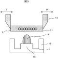
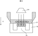
- FIG. 3 and 4 are both A-A 'cross-sectional views of FIG.
- the fiber block 3 is gripped by a manipulator 19 capable of fine alignment.
- the manipulator 19 is operated to adjust the position so that the optical coupling between the optical element 6 mounted on the substrate and the lens 4 on the fiber block 3 is the best (arrow B).
- the manipulator 19 is moved in the ⁇ Z direction so that the bottom surface 31 of the fiber block 3 is in contact with the protrusion 15 of the substrate 1 (arrow C).
- the adhesive 14 is sandwiched between the substrate protrusion 16 and the fiber block 3.
- UV light is irradiated from a UV light source 24 installed above the fiber block 3, and the UV light passes through the fiber block 3 to cure the adhesive 14.
- the gripping of the fiber block 3 with the manipulator 19 is released.
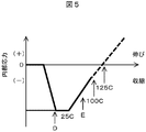
- the adhesive 14 undergoes volume shrinkage of about 5% accompanying cure shrinkage.
- the thickness of the adhesive in the z direction cannot shrink because the fiber block 3 is in direct contact with the protrusion 15 as shown in FIG. Thereby, after the adhesive 14 is solidified, the shrinkage pressure is included in the adhesive 14.
- the shrinkage pressure is included in the adhesive (arrow D).
- the adhesive 14 is stressed in the direction extending in the + z direction due to thermal expansion.
- the adhesive 14 contains a shrinkage stress, it simply releases the compressive stress as the temperature rises, and does not expand (arrow E).
- the thermal expansion coefficient of the adhesive 14 is about 50 PPM / ° C. Therefore, a temperature increase of 125 ° C. is necessary to completely release the shrinkage stress.
- the upper limit temperature of the optical module 100 is 100 ° C. or lower, the shrinkage stress is always applied to the adhesive at the operating temperature of the optical module. Therefore, the height change of the fiber block 3 in the z direction does not occur.
- the adhesive 14 provided on the upper surface of the protrusion 16 is bonded to the fiber block 3 with a flat bonding surface 32 having no step in the z direction.
- the adhesive expands due to the temperature rise, the side surface of the adhesive 14 is not restrained because it is in contact with the air 18 and can expand freely. From this, the adhesive 14 does not apply stress to the fiber block 3.
- the bonding surface 32 of the fiber block is in a flat state without a step.
- the force that the bonding surface 32 receives from the expansion of the adhesive 14 is only the shear stress from the bonding interface. Since the adhesive interface 32 has a circular shape, the force received from the adhesive interface is isotropic, and the sum of stresses that cause displacement in the xy plane of the fiber block 3 is cancelled. Therefore, no positional deviation occurs in the xy plane.
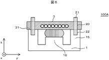
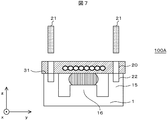
- the board 1 of the optical module 100 ⁇ / b> A is provided with a fitting hole 22 in the protrusion 15 in addition to the protrusion 15 and the protrusion 16.
- the fiber block 3 is also provided with a fitting hole 20.
- the optical element 6 and the lens 4 can be aligned by passing the fitting pin 21 through both the fitting hole 20 and the fitting hole 22. Accordingly, the alignment of the fiber block 3 in the xy direction can be easily performed without using the manipulator 19 as shown in FIGS. 4 and 5 of the first embodiment.
- the adhesive 14 exists between the upper surface of the protrusion 16 and the adhesive surface 32 of the fiber block 3 as described in the first embodiment.
- the bonding surface on the bottom surface of the fiber block is flat without a step in the z direction.
- the upper surface of the protrusion 15 is in direct contact with the fiber block bottom surface 31. Thereby, the height of the fiber block in the z direction is determined by H_b1.
- Example 2 it is possible to include compressive stress inside the adhesive by curing the adhesive 14 in the assembly process described in FIGS. 3 and 4 of Example 1.
- the positional deviation of the fiber block in the z direction is the same as that of the first embodiment described with reference to FIG.
- the fitting pin 21 can be removed.
- the optical module 100 ⁇ / b> A can align the fiber block 3 using the fitting pin 21, and can pull out the fitting pin 21 after fixing by fixing the adhesive 14. Therefore, in the optical module 100A, as shown in FIG. 7, the fitting pin 21 does not exist, but the fitting hole 20 and the fitting hole 22 remain.
- the fiber block 3 is aligned with the fitting pin 21, and the fitting pin 21 is pulled out after the fixing with the adhesive 14 is completed. Further, even if the temperature changes after the fitting pin 21 is extracted, no stress in the xy plane is applied to the substrate 1. According to the second embodiment, an optical module that does not require the use of a manipulator in its manufacture can be obtained.
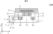
- the adhesive 23 remains between the side surface of the protrusion 15 and the side surface of the protrusion 16.
- the thickness H_s of the adhesive 23 is lower than the side surface height (H_b2-H_b3) of the protrusion 16, that is, there is a relationship of H_s ⁇ H_b1.
- the adhesive 23 does not contact the bottom surface 31 of the fiber block. Therefore, the upper surface of the protrusion 15 is in direct contact with the bottom surface 31 of the fiber block.
- the adhesive 23 In the adhesive 23 surrounded by the protrusions 15 and 16, even if the thermal expansion of the adhesive 23 due to a temperature rise occurs, the air layer 18 exists in the z direction.
- the stress applied to the fiber block 3 is the same as in the first embodiment. In the xy plane, the adhesive 23 applies stress to the side surfaces of the protrusions 15 or 16, but does not apply stress to the fiber block 3. According to the third embodiment, it is not necessary to accurately control the application amount of the adhesive 14 described with reference to FIG.
Landscapes
- Physics & Mathematics (AREA)
- General Physics & Mathematics (AREA)
- Optics & Photonics (AREA)
- Optical Couplings Of Light Guides (AREA)
Abstract
L'objectif de la présente invention consiste à pourvoir à un module optique doté d'une structure simple et compacte, de manière que même lorsque la température du module optique se modifie, un bloc de fibres ne change pas de position. Le module optique comprend : un élément optique qui est un élément de transmission ou un élément de réception ; un semi-conducteur destiné à commander un élément optique ou à amplifier la sortie de l'élément optique ; un substrat de câblage connecté électriquement à l'élément optique et au semi-conducteur ; et un bloc de fibres connecté optiquement à l'élément optique. Le substrat de câblage comprend une pluralité de premières saillies en contact avec le bloc de fibres et une seconde saillie plus courte que la première saillie. La seconde saillie et le bloc de fibres sont connectés à l'aide d'un adhésif photodurcissable.
Priority Applications (1)
| Application Number | Priority Date | Filing Date | Title |
|---|---|---|---|
| PCT/JP2013/065632 WO2014196043A1 (fr) | 2013-06-05 | 2013-06-05 | Module optique et son procédé de fabrication |
Applications Claiming Priority (1)
| Application Number | Priority Date | Filing Date | Title |
|---|---|---|---|
| PCT/JP2013/065632 WO2014196043A1 (fr) | 2013-06-05 | 2013-06-05 | Module optique et son procédé de fabrication |
Publications (1)
| Publication Number | Publication Date |
|---|---|
| WO2014196043A1 true WO2014196043A1 (fr) | 2014-12-11 |
Family
ID=52007719
Family Applications (1)
| Application Number | Title | Priority Date | Filing Date |
|---|---|---|---|
| PCT/JP2013/065632 Ceased WO2014196043A1 (fr) | 2013-06-05 | 2013-06-05 | Module optique et son procédé de fabrication |
Country Status (1)
| Country | Link |
|---|---|
| WO (1) | WO2014196043A1 (fr) |
Cited By (3)
| Publication number | Priority date | Publication date | Assignee | Title |
|---|---|---|---|---|
| WO2020088011A1 (fr) * | 2018-11-02 | 2020-05-07 | 青岛海信宽带多媒体技术有限公司 | Sous-ensemble optique récepteur et module optique |
| CN114522892A (zh) * | 2021-12-31 | 2022-05-24 | 武汉英飞光创科技有限公司 | 具有awg的光模块的耦合方法以及装置 |
| CN115755289A (zh) * | 2022-11-02 | 2023-03-07 | 武汉英飞光创科技有限公司 | 光模块透镜耦合的吸嘴、装置以及方法 |
Citations (4)
| Publication number | Priority date | Publication date | Assignee | Title |
|---|---|---|---|---|
| JPH10325917A (ja) * | 1997-05-26 | 1998-12-08 | Matsushita Electric Ind Co Ltd | 光受信装置とその製造方法 |
| JP2005062645A (ja) * | 2003-08-19 | 2005-03-10 | Toppan Printing Co Ltd | 光接続構造体およびその製造方法 |
| JP2006011046A (ja) * | 2004-06-25 | 2006-01-12 | Sony Corp | 光導波路及びその光導波モジュール、並びに光伝送モジュール |
| JP2009198804A (ja) * | 2008-02-21 | 2009-09-03 | Sony Corp | 光モジュール及び光導波路 |
-
2013
- 2013-06-05 WO PCT/JP2013/065632 patent/WO2014196043A1/fr not_active Ceased
Patent Citations (4)
| Publication number | Priority date | Publication date | Assignee | Title |
|---|---|---|---|---|
| JPH10325917A (ja) * | 1997-05-26 | 1998-12-08 | Matsushita Electric Ind Co Ltd | 光受信装置とその製造方法 |
| JP2005062645A (ja) * | 2003-08-19 | 2005-03-10 | Toppan Printing Co Ltd | 光接続構造体およびその製造方法 |
| JP2006011046A (ja) * | 2004-06-25 | 2006-01-12 | Sony Corp | 光導波路及びその光導波モジュール、並びに光伝送モジュール |
| JP2009198804A (ja) * | 2008-02-21 | 2009-09-03 | Sony Corp | 光モジュール及び光導波路 |
Cited By (3)
| Publication number | Priority date | Publication date | Assignee | Title |
|---|---|---|---|---|
| WO2020088011A1 (fr) * | 2018-11-02 | 2020-05-07 | 青岛海信宽带多媒体技术有限公司 | Sous-ensemble optique récepteur et module optique |
| CN114522892A (zh) * | 2021-12-31 | 2022-05-24 | 武汉英飞光创科技有限公司 | 具有awg的光模块的耦合方法以及装置 |
| CN115755289A (zh) * | 2022-11-02 | 2023-03-07 | 武汉英飞光创科技有限公司 | 光模块透镜耦合的吸嘴、装置以及方法 |
Similar Documents
| Publication | Publication Date | Title |
|---|---|---|
| US10466433B2 (en) | Optical module including silicon photonics chip and coupler chip | |
| JP6029115B2 (ja) | 光デバイス、光コネクタ・アセンブリおよび光接続方法 | |
| US9541715B2 (en) | Optical module, manufacturing method of optical module, and optical device | |
| US8827572B2 (en) | Side coupling optical fiber assembly and fabrication method thereof | |
| JP7117133B2 (ja) | 光サブアセンブリ及びその製造方法並びに光モジュール | |
| US7627210B2 (en) | Manufacturing method of optical-electrical substrate and optical-electrical substrate | |
| CN100392460C (zh) | 光传送模块及其制造方法 | |
| US8615149B2 (en) | Photonics chip with efficient optical alignment and bonding and optical apparatus including the same | |
| CN103430067A (zh) | 光学引擎 | |
| JP2009198804A (ja) | 光モジュール及び光導波路 | |
| JP2011095295A (ja) | 光モジュールの光ファイバブロックおよびその製造方法 | |
| JP4704126B2 (ja) | 光モジュール | |
| JP2018004830A (ja) | 高耐熱性光ファイバモジュールおよびその作製方法 | |
| WO2014196043A1 (fr) | Module optique et son procédé de fabrication | |
| JP5400421B2 (ja) | 光デバイス及びその製造方法 | |
| JP2007072007A (ja) | 光導波路モジュール | |
| JP2013057720A (ja) | 光モジュール | |
| US10073226B2 (en) | Method for coupling an optical fiber to an optical or optoelectronic component | |
| JP2017167260A (ja) | 光デバイス、回路モジュール、及び光接続部品の実装方法 | |
| JP2006120781A (ja) | 光電変換モジュール | |
| WO2021009911A1 (fr) | Procédé d'alignement d'élément guide d'ondes optique | |
| JP2011095294A (ja) | 光モジュール | |
| KR101175300B1 (ko) | 광 모듈 및 그 제조방법 | |
| JP2012226100A (ja) | 光回路 | |
| JP2010286549A (ja) | 光信号処理回路、光信号処理回路付半導体装置および光信号処理回路の製造方法 |
Legal Events
| Date | Code | Title | Description |
|---|---|---|---|
| 121 | Ep: the epo has been informed by wipo that ep was designated in this application |
Ref document number: 13886570 Country of ref document: EP Kind code of ref document: A1 |
|
| NENP | Non-entry into the national phase |
Ref country code: DE |
|
| 122 | Ep: pct application non-entry in european phase |
Ref document number: 13886570 Country of ref document: EP Kind code of ref document: A1 |
|
| NENP | Non-entry into the national phase |
Ref country code: JP |