WO2014196233A1 - Procédé de fabrication de nanoparticules, et matériau thermoélectrique ainsi que procédé de fabrication de celui-ci - Google Patents
Procédé de fabrication de nanoparticules, et matériau thermoélectrique ainsi que procédé de fabrication de celui-ci Download PDFInfo
- Publication number
- WO2014196233A1 WO2014196233A1 PCT/JP2014/054868 JP2014054868W WO2014196233A1 WO 2014196233 A1 WO2014196233 A1 WO 2014196233A1 JP 2014054868 W JP2014054868 W JP 2014054868W WO 2014196233 A1 WO2014196233 A1 WO 2014196233A1
- Authority
- WO
- WIPO (PCT)
- Prior art keywords
- layer
- nanoparticles
- base material
- annealing
- thickness
- Prior art date
- Legal status (The legal status is an assumption and is not a legal conclusion. Google has not performed a legal analysis and makes no representation as to the accuracy of the status listed.)
- Ceased
Links
Images






Classifications
-
- H—ELECTRICITY
- H10—SEMICONDUCTOR DEVICES; ELECTRIC SOLID-STATE DEVICES NOT OTHERWISE PROVIDED FOR
- H10N—ELECTRIC SOLID-STATE DEVICES NOT OTHERWISE PROVIDED FOR
- H10N10/00—Thermoelectric devices comprising a junction of dissimilar materials, i.e. devices exhibiting Seebeck or Peltier effects
- H10N10/80—Constructional details
- H10N10/85—Thermoelectric active materials
- H10N10/857—Thermoelectric active materials comprising compositions changing continuously or discontinuously inside the material
-
- H—ELECTRICITY
- H10—SEMICONDUCTOR DEVICES; ELECTRIC SOLID-STATE DEVICES NOT OTHERWISE PROVIDED FOR
- H10N—ELECTRIC SOLID-STATE DEVICES NOT OTHERWISE PROVIDED FOR
- H10N10/00—Thermoelectric devices comprising a junction of dissimilar materials, i.e. devices exhibiting Seebeck or Peltier effects
- H10N10/01—Manufacture or treatment
-
- H—ELECTRICITY
- H10—SEMICONDUCTOR DEVICES; ELECTRIC SOLID-STATE DEVICES NOT OTHERWISE PROVIDED FOR
- H10N—ELECTRIC SOLID-STATE DEVICES NOT OTHERWISE PROVIDED FOR
- H10N10/00—Thermoelectric devices comprising a junction of dissimilar materials, i.e. devices exhibiting Seebeck or Peltier effects
- H10N10/80—Constructional details
- H10N10/85—Thermoelectric active materials
- H10N10/851—Thermoelectric active materials comprising inorganic compositions
- H10N10/855—Thermoelectric active materials comprising inorganic compositions comprising compounds containing boron, carbon, oxygen or nitrogen
-
- H—ELECTRICITY
- H10—SEMICONDUCTOR DEVICES; ELECTRIC SOLID-STATE DEVICES NOT OTHERWISE PROVIDED FOR
- H10N—ELECTRIC SOLID-STATE DEVICES NOT OTHERWISE PROVIDED FOR
- H10N10/00—Thermoelectric devices comprising a junction of dissimilar materials, i.e. devices exhibiting Seebeck or Peltier effects
- H10N10/80—Constructional details
- H10N10/85—Thermoelectric active materials
- H10N10/851—Thermoelectric active materials comprising inorganic compositions
- H10N10/8556—Thermoelectric active materials comprising inorganic compositions comprising compounds containing germanium or silicon
-
- B—PERFORMING OPERATIONS; TRANSPORTING
- B82—NANOTECHNOLOGY
- B82Y—SPECIFIC USES OR APPLICATIONS OF NANOSTRUCTURES; MEASUREMENT OR ANALYSIS OF NANOSTRUCTURES; MANUFACTURE OR TREATMENT OF NANOSTRUCTURES
- B82Y40/00—Manufacture or treatment of nanostructures
Definitions
- the present invention relates to a method for producing nanoparticles, a method for producing a thermoelectric material, and a thermoelectric material produced by the production method.
- thermoelectric material converts a temperature difference (thermal energy) into electric energy
- performance of the thermoelectric material is represented by a performance index Z expressed by the following equation (1).
- ⁇ is the Seebeck coefficient (V / K) of the thermoelectric material
- S is the conductivity (S / m) of the thermoelectric material
- ⁇ is the thermal conductivity (W / mK) of the thermoelectric material.
- Z has a dimension of the reciprocal of temperature, and ZT obtained by multiplying the figure of merit Z by the absolute temperature T is a dimensionless value. This ZT is called a dimensionless figure of merit and is used as an index representing the performance of the thermoelectric material.
- thermoelectric materials In order to use thermoelectric materials widely, it is required to further improve their performance. From the formula (1), it can be seen that an increase in Seebeck coefficient, an increase in electrical conductivity, and a decrease in thermal conductivity are effective for improving the performance of thermoelectric materials.
- the Seebeck coefficient and thermal conductivity can be controlled by reducing the number of carriers and increasing phonon scattering by quantum wells and quantum wires (for example, LDHicks et al., PRB 47 (1993) 12727 ( Non-Patent Document 1), LDHicks et al., PRB 47 (1993) 16631 (Non-Patent Document 2)) and have been demonstrated (for example, LDHicks et al., PRB (1996) R10493 (Non-Patent Document 3) ), Y.Okamoto et al., JJAP 38 (1999) L946 (Non-Patent Document 4)).
- thermoelectric materials in which the carrier is further reduced in size by forming particles are known (Japanese Patent Laid-Open No. 2003-31860 (Patent Document 1), Japanese Patent Laid-Open No. 2002-76452 (Patent Document 2)). JP, 2011-3741, A (Patent Document 3)), it was difficult to sufficiently improve the thermoelectric characteristics due to large variation in particle diameter or failure to control the particle diameter.
- Non-Patent Document 5 annealing a SiGeAu thin film to form SiGe nanoparticles in the thin film improves thermoelectric properties compared to bulk SiGe.
- An object of this invention is to provide the manufacturing method of the nanoparticle which forms the nanoparticle which comprises the thermoelectric material which has the more excellent thermoelectric characteristic, the manufacturing method of a thermoelectric material, and a thermoelectric material.
- Non-Patent Document 5 As a result of intensive research, the inventors of the present invention have found that nanoparticles produced by the method described in Non-Patent Document 5 have overlapping wave functions of carriers (free electrons or free holes) because the distance between the nanoparticles is too close. It has been found that an increase in the amount of integration does not cause a sufficient quantum effect, that is, a quantum increase in the state density, and therefore the Seebeck coefficient cannot be sufficiently improved. And this inventor discovered the method of controlling so that the space
- the present invention is a method for producing nanoparticles in which a base material composed of a semiconductor material composed of a base material element forms nanoparticles containing a base material element and a different element different from the base material element, A stacking process in which first layers containing different elements and second layers not containing different elements are alternately stacked, and a stacked body in which the first layer and the second layer are stacked is annealed to form a base material. And an annealing step for forming nanoparticles, and in the laminating step, all the base material elements are contained in at least one of the first layer and the second layer, and the second layer is formed thicker than the first layer.
- the base element is Si and Ge, the different element is Au, Cu, B, or Al.
- the first layer includes Ge as a base element, The layer contains Si as the base material element.
- the base element is N and Ga, and the different element is In or Al.
- the first layer and the second layer have N and Ga as base elements. Including.
- the thickness of the first layer is preferably 2 to 8 nm, and the nanoparticles formed in the annealing step have an average particle size of preferably 1 to 25 nm and an average interval of preferably 3 ⁇ 25 nm.
- the annealing step may be performed after the lamination step or simultaneously with the lamination step.
- the present invention is also a method for producing a thermoelectric material comprising nanoparticles containing a base material element and a different element different from the base material element in a thin film made of a semiconductor material composed of the base material element.
- a lamination step of alternately laminating a first layer containing an element and a second layer not containing a different element, and annealing the laminated body in which the first layer and the second layer are laminated to form nanoparticles in the thin film
- all the base material elements are included in at least one of the first layer and the second layer, and the second layer is formed thicker than the first layer.
- the present invention is a thermoelectric material manufactured by the above-described method for manufacturing a thermoelectric material.
- the average particle diameter of the nanoparticles is preferably 1 to 25 nm, and the average interval of the nanoparticles is preferably 3 to 25 nm.
- thermoelectric material exhibiting excellent thermoelectric properties can be obtained by using a material containing nanoparticles produced by the production method of the present invention as a thermoelectric material.
- FIG. 7A is a diagram illustrating a diffraction image of the high-resolution TEM image of FIG. 6, and FIG. 7B is a diagram illustrating imaging in a specific direction different from FIG.
- FIG. 7B obtained by Fourier transform of the diffraction image. It is a figure which shows the high-resolution TEM image after an annealing process about the sample of the comparative example 1.
- FIG. (A) shows a diffraction image of the high-resolution TEM image of FIG. 9, and (B) shows an image in a specific direction obtained by Fourier transform of the diffraction image.
- A) A diffraction image of the high-resolution TEM image of FIG. 9 is shown, and (B) is a diagram showing imaging in a specific direction different from FIG. 10 (B) obtained by Fourier transform of the diffraction image. It is a figure which shows the measurement result of a Seebeck coefficient. It is a figure which shows the measurement result of thermal conductivity.
- FIG. 6 is a graph plotting the relationship between the film thickness of the first layer and the grain spacing calculated by the measuring method 4.
- the present invention relates to a method for producing nanoparticles in which a base material composed of a semiconductor material composed of a base material element forms nanoparticles containing a base material element and a different element different from the base material element.
- a base material composed of a semiconductor material composed of a base material element forms nanoparticles containing a base material element and a different element different from the base material element.
- Laminating the first layer containing the elements and the second layer not containing the different elements alternately, and annealing the laminated body in which the first layer and the second layer are laminated.
- an annealing step for forming the nanoparticles In the laminating step, all the base material elements are included in at least one of the first layer and the second layer, and the second layer is formed thicker than the first layer.
- the thickness T 2 of the second layer is thicker than the thickness T 1 of the first layer, and preferably satisfies the relationship of T 1 ⁇ T 2 ⁇ 3T 1 .
- the desired particle spacing of the nanoparticles when the G d is formed in the laminating step, the thickness T 2 of the second layer, determined so as to satisfy the following equation (2) It is preferable to do.
- the thickness T 2 of the second layer determined in this way nanoparticles that satisfy the following formula (3) can be formed through the annealing step, in which the average particle spacing G m of the nanoparticles satisfies the following formula (3). it can.
- the derivation process of Formula (2) and Formula (3) will be described later.
- Average interval G m of the nanoparticles produced by the production method of the present invention is preferably 3 ⁇ 25 nm, more preferably from 3 ⁇ 10 nm. By setting such a grain interval, a high Seebeck coefficient and a large dimensionless figure of merit ZT can be obtained.
- the nanoparticle interval referred to in this specification refers to the shortest interval from one end to the other of the particles measured from an electron microscope (two-dimensional planar projection image), and the average interval refers to a sufficient number of particle intervals.
- the arithmetic mean of In this application, the arithmetic average of the intervals of 22 particles was calculated as the average interval. The interval between the nanoparticles can be adjusted by the thickness of the second layer.
- the thickness T 1 of the first layer is determined so as to satisfy the following formula (4) in the stacking step. Is preferred. Incidentally, by adopting the thickness T 1 of the first layer thus determined, through an annealing process, the average particle diameter X m of nanoparticles to form nanoparticles that satisfies Equation (5) below it can. The derivation process of Formula (4) and Formula (5) will be described later.
- the average particle diameter X m of the nanoparticles produced by the production method of the present invention is preferably 1 ⁇ 25 nm, more preferably 5 ⁇ 25 nm. By setting it as such a particle size, a high Seebeck coefficient and a large dimensionless figure of merit ZT can be obtained.
- the particle diameter means the long diameter of the particle measured from an image (two-dimensional planar projection image) obtained with an electron microscope, and the average particle diameter is a particle diameter of a sufficient number of particles. Arithmetic mean. In the present application, the arithmetic average of the particle sizes of 22 particles was calculated as the average particle size.
- the particle size of the nanoparticles is the thickness of the first layer, the thickness of the second layer, the atomic concentration of the different elements contained in the first layer, and the conditions for annealing treatment of the laminate in which the first layer and the second layer are laminated. It can be adjusted by etc.
- the thickness of the first layer is preferably 2 to 8 nm, and the thickness of the second layer is preferably 2.5 to 12 nm.
- Examples of the semiconductor material used as the base material in the manufacturing method include silicon germanium, gallium nitride, aluminum nitride, boron nitride, bismuth / tellurium: Bi 2 Te 3 , Pb 2 Te 3 , magnesium / silicide, and the like.
- the base material is silicon germanium
- the base material elements are Si and Ge
- examples of the different elements include Au, Cu, B, Al, and P.
- the base material is gallium nitride
- the base material elements are N and Ga
- examples of the different elements include In, Al, and B.
- the base material elements are Bi and Te or Pb, and examples of the different elements include Au, Cu, B, Al, and P.
- the base material elements are Mg and Si, and examples of the different elements include Au, Cu, B, Al, and P.
- a molecular beam epitaxy method MBE; Molecular Beam Epitaxy
- an electron beam method EB; Electron Beam
- a sputtering method a metal organic vapor phase epitaxy method (MOVPE;
- MOVPE metal organic vapor phase epitaxy method
- the atomic concentration of the different element in the first layer is preferably 0.5 to 50 atomic%.
- the first layer may be a single layer or multiple layers. In the case of a multilayer, a stacked body of a layer containing a base material element and a layer containing a different element may be used.
- the first layer and the second layer are included in at least one of the first layer and the second layer.
- the first layer can be formed so as to include Ge as a base material element
- the second layer may include Si as a base material element.
- both the first layer and the second layer can be formed to contain N and Ga.
- the first layer and the second layer may be stacked alternately, for example, the first layer and the second layer may be stacked 1 to 1000 times. The number of times the first layer is stacked substantially matches the number of nanoparticles in the thickness direction to be formed.
- the laminated body in which the first layer and the second layer are laminated is annealed to form nanoparticles in the base material.
- the annealing treatment here refers to a treatment of heating and then cooling until the atoms of the first layer diffuse. Therefore, the temperature and time of the annealing process vary depending on the material of the first layer. In addition, by controlling the temperature, time, and heating rate of the annealing treatment, the presence / absence of nanoparticle formation and the particle size of the formed nanoparticle can be adjusted.
- the lamination process and the annealing process may be performed independently or simultaneously.
- the annealing process is performed after the lamination process of alternately laminating the first layer and the second layer is completed. If they are performed simultaneously, the lamination process is performed under the conditions of the annealing process, and the annealing process is performed simultaneously in the lamination process.
- temperature control is easy, while when performed simultaneously, the number of steps can be reduced.
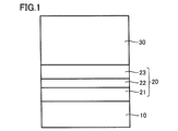
- FIG. 1 is a cross-sectional view schematically showing a laminated body in a state where the laminating process is completed once and an annealing process is not yet performed.
- a sapphire substrate 10 is prepared, and deposited in the order of Ge, Au, and Ge by the MBE method to form an amorphous Ge (a-Ge) layer 21 / Au layer 22 / amorphous Ge (a- A first layer 20 made of a Ge) layer 23 is formed, and then Si is deposited to form a second layer 30 made of an amorphous Si (a-Si) layer.
- a-Ge amorphous Ge
- Au amorphous Ge
- Si amorphous Si
- Each raw material of Ge, Au, and Si is heated by an electron beam method in the cell to create a molecular beam.
- Such stacking of the first layer 20 and the second layer 30 is repeated 60 times to form a stacked body.
- the a-Ge layer 21 and the Au layer 22 are formed as separate layers in the first layer 20, but Ge and The deposition method is not limited as long as it is formed so as to include Au.
- the laminate is annealed to form nanoparticles.
- SiGe nanoparticles containing Au are formed in the base material made of Si and Ge.
- the mechanism for forming nanoparticles in this way is as follows. First, AuGe having a lower eutectic point than AuSi is activated in the first layer 20, and then the Si contained in the second layer 30 is taken in to form Au. It is understood that SiGe nanoparticles containing are formed.
- the base material composed of Si and Ge around the SiGe nanoparticles is amorphous SiGe, amorphous Ge, or amorphous Si.
- the thickness of the first layer 20 is 2.0 nm or more and less than 5.0 nm, and the thickness of the second layer 30 is 3.0 nm. It is preferable that the thickness of the Au layer 22 in the first layer 20 is 0.1 nm or more and 0.4 nm or less.
- the atomic concentration of Au in the first layer 20 is preferably 0.5 to 50 atomic%.
- the temperature of the annealing treatment in the annealing step can be appropriately selected from the range of 200 to 800 ° C., but in order to obtain nanoparticles having a particle size of 5 to 25 nm, the temperature of the annealing treatment is 300 to 700 ° C. Preferably there is.
- the particle size of the nanoparticles depends on the thickness of the first layer 20 and the second layer 30 and the atomic concentration of the different elements. For example, when the annealing temperature is 250 ° C., the nanoparticle size is 0.1 to 2 nm. When it is easy to obtain particles and the annealing temperature is 750 ° C., it is easy to obtain nanoparticles having a particle size of 20 to 100 nm.
- the annealing time in the annealing process performed after the lamination process is completed can be set to 1 to 120 minutes, for example.
- thermoelectric material As described above, in the base material composed of Si and Ge, a thin film containing Au-containing SiGe nanoparticles is formed, and when this is used as a thermoelectric material, it does not contain nanoparticles. Compared with, the thermal conductivity decreases, the Seebeck coefficient increases, and it functions as a thermoelectric material with a high figure of merit. The increase in the Seebeck coefficient is due to the occurrence of grain boundary scattering due to the presence of nanoparticles and the ability to confine carriers more effectively in the nanoparticles. Furthermore, according to the production method of the present invention, the interval between the nanoparticles can be optimized, and thereby grain boundary scattering can be more effectively generated, and thus the Seebeck coefficient can be further increased.
- the second embodiment is an example of the manufacturing method of the present invention when the base material is gallium nitride and the different element is In.
- FIG. 2 is a cross-sectional view schematically showing a stacked body in a state where the stacking process is completed once and an annealing process is not yet performed.
- a sapphire substrate 10 is prepared, Ga, N, and In are deposited by MBE to form a first layer 40 made of an amorphous InGaN (a-InGaN) layer, and then Ga. , N is deposited to form a second layer 50 made of an amorphous GaN (a-GaN) layer.
- a-InGaN amorphous InGaN
- a-GaN amorphous GaN
- the laminate is annealed to form nanoparticles.
- GaN nanoparticles containing In are formed in the base material composed of Ga and N.
- the base material composed of Ga and N around the GaN nanoparticles is amorphous GaN.
- the thickness of the first layer 40 is 2.5 nm or more and less than 3.0 nm, and the thickness of the second layer 50 is 4.0 nm.
- the thickness is preferably 6.0 nm or less.
- the atomic concentration of In in the first layer 40 is preferably 0.1 to 80 atomic%.
- the temperature of the annealing treatment in the annealing step can be appropriately selected from the range of 150 to 1100 ° C. However, in order to obtain nanoparticles having a particle size of 1 to 10 nm, the temperature of the annealing treatment is 300 to 800 ° C. Preferably there is.
- the annealing time in the annealing process performed after the lamination process is completed can be set to 1 to 120 minutes, for example.
- thermoelectric material As described above, in the base material composed of Ga and N, a thin film including GaN nanoparticles containing In is formed, and when this is used as a thermoelectric material, it is not included by including nanoparticles. Compared with, the thermal conductivity decreases, the Seebeck coefficient increases, and it functions as a thermoelectric material with a high figure of merit. The increase in Seebeck coefficient is due to the occurrence of grain boundary scattering due to the presence of nanoparticles and the ability to effectively confine carriers in the nanoparticles. Furthermore, according to the production method of the present invention, the interval between the nanoparticles can be optimized, and thereby grain boundary scattering can be more effectively generated, and thus the Seebeck coefficient can be further increased.
- thermoelectric material of the present invention is a manufacturing method in which the thin film containing nanoparticles formed by annealing the laminate is used as it is in the above-described manufacturing method of nanoparticles. That is, the method for manufacturing a thermoelectric material of the present invention is a method for manufacturing a thermoelectric material including nanoparticles containing a base material element and a different element different from the base material element in a thin film made of a semiconductor material composed of the base material element.
- thermoelectric material composed of nanoparticles comprising: a laminating step of alternately laminating a first layer containing a different element and a second layer not containing the different element; An annealing step of annealing the laminated body in which the two layers are laminated to form nanoparticles in the thin film.
- all the base material elements are included in at least one of the first layer and the second layer, and the second layer is formed thicker than the first layer.
- the details of the laminating step and the annealing step are as described in the method for producing nanoparticles.
- thermoelectric material of the present invention is a thermoelectric material produced by the method for producing a thermoelectric material. That is, the thermoelectric material of the present invention contains nanoparticles, the average particle diameter of the nanoparticles is preferably 1 to 25 nm, more preferably 5 to 25 nm, and the interval between the nanoparticles is preferably 3 to 25 nm, more preferably 3 ⁇ 10 nm.
- a thermoelectric material having nanoparticles with such a particle spacing and particle size can obtain a high Seebeck coefficient and a large dimensionless figure of merit ZT.
- the Seebeck coefficient is preferably 3 mV / K or more, and the dimensionless figure of merit ZT is preferably 10 or more.
- Nanoparticles were formed by the manufacturing method of the first embodiment. Specifically, in the stacking step, a first layer composed of an a-Ge layer / Au layer / a-Ge layer is formed on a sapphire substrate, and each layer has a thickness of 1.3 to 1.9 nm / 0.2 nm / 1. Deposition was performed at 3 to 1.9 nm, and then Si was deposited to form a second layer composed of an a-Si layer in a thickness range of 2.6 to 5.2 nm. The concentration of Au in the first layer was 2.5 to 17 atomic%. And the process of laminating the first layer and the second layer was repeated 60 times.
- the laminate was left in an RTA furnace in a nitrogen atmosphere in an environment of 600 ° C. for 15 minutes to perform an annealing treatment and an annealing process was performed to form nanoparticles.
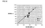
- the equation (2) and ( The relational expression 3) was derived from samples prepared by, for example, as measurement method 1-3 described below.
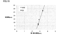
- the equation (4) and ( The relational expression 5) was derived from samples prepared by, for example, as measurement method 4 described below.
- MBE molecular beam epitaxy
- EB method electron beam method
- the nanoparticles in the samples prepared by the measurement method 1-3 in the following manner to calculate the mean particle spacing G m, the relationship between the average particle distance G m and the thickness of the second layer in FIGS. 16 to 18 Plotted. Further, the nano-particles in the sample prepared by the measurement method 4, as follows to calculate the average particle diameter X m, a plot of average particle relationship size X m and the thickness of the first layer in FIG. 19.
- the measurement method 1 is a high-resolution TEM (Transmission Electron Microscopy) obtained after thinning to about 100 nm in the stacking direction by FIB (Focused Ion Beam) using an electron microscope (device name: JEM-2100F, manufactured by JEOL Ltd.). ) Image and an FFT image obtained by performing FFT (Fast Fourier Transform) transform and processing to make the periodic structure of the nanocrystal stand out, an average grain spacing G was calculated.
- Measurement method 4 In measurement method 4, the particle size X of the nanoparticles was calculated by Scherrer's equation based on the measurement result of X-ray diffraction (XRD). Table 1 shows the data of the designed film thickness of the first layer and the particle size X calculated by the measuring method 4 for six samples (Sample 1 to Sample 6), and FIG. 19 is a plot of the results of Table 1. is there.
- Nanoparticles were formed by the manufacturing method of the first embodiment. Specifically, in the stacking step, the first layer composed of the a-Ge layer / Au layer / a-Ge layer is formed on the sapphire substrate, and the thickness of each layer is 1.3 nm / 0.2 nm / 1.3 nm. Deposition was performed so as to have a thickness of 2.8 nm, and then Si was deposited, so that a second layer composed of an a-Si layer was deposited so as to have a thickness of 5.2 nm. And this process was repeated 60 times. Note that the atomic concentration of Au in the first layer was 2.5 atomic%.
- the laminated body was left to stand in an environment of 600 ° C. for 15 minutes in an RTA furnace in a nitrogen atmosphere to perform an annealing process to perform an annealing process.
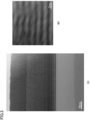
- FIG. 3A shows a bright field STEM (Scanning Transmission Electron Microscopy) image obtained using an electron microscope (device name: JEM-2100F, manufactured by JEOL Ltd.) after the lamination process and before the annealing process.
- FIG. 3B shows an enlarged image of the stacked portion of the first layer and the second layer in FIG. 3A and 3B, it was confirmed that the first layer and the second layer were alternately stacked.
- EDX energy dispersive X-ray spectroscopy
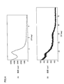
- FIG. 4 shows an X-ray diffraction pattern obtained by X-ray diffraction measurement performed using an X-ray diffractometer on the laminate after the lamination step and before the annealing step
- FIG. FIG. 4B shows a diffraction pattern on the high angle side
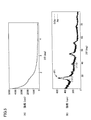
- 5 shows an X-ray diffraction pattern of the laminated body after the annealing step
- FIG. 5A shows a low-angle diffraction pattern
- FIG. 5B shows a high-angle diffraction pattern.
- a peak was observed before the annealing step (FIG. 4A), but the peak disappeared after the annealing step (FIG. 5A).
- the peak on the low angle side corresponds to the periodic structure in which the first layer and the second layer are repeatedly laminated, and this periodic structure was presumed to have disappeared by the annealing process.
- the peak P1 observed in FIG. 5 (B) corresponds to the crystal plane (111) of the SiGe crystal, and thus it was assumed that the SiGe crystal was formed by the annealing treatment.
- FIG. 6 was obtained after the laminated body after the annealing process was thinned to about 100 nm by FIB (Focused Ion Beam) in the stacking direction using an electron microscope (device name: JEM-2100F, manufactured by JEOL Ltd.).
- a high resolution TEM (Transmission Electron Microscopy) image is shown.
- FIG. 6 a region surrounded by a dotted line is a region estimated to be crystallized.
- FIGS. 7A and 8A show diffraction images of the high-resolution TEM image of FIG. 6, and FIGS. 7B and 8B show FIGS. 7A and 8A, respectively.
- Fig. 4 shows imaging in different specific directions obtained by Fourier transform of a diffraction image.
- the grain size of the crystal grains was 5 to 14 nm, and the average grain size was 8 nm.
- the peak P1 corresponding to the crystal plane of SiGe is estimated to be 8.2 nm by applying the half width to Scherrer's formula and estimating the grain size of the crystal grains. It almost coincided with the actually measured value in the high resolution TEM image shown in FIG.
- the crystal grain interval was measured, it was 5 to 25 nm, and the average interval was 14 nm.
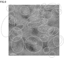
- Nanoparticles were produced by the same production method as in Example 1 except that the thickness of the second layer in the laminating step was 2.6 nm, that is, the thickness was made thinner than 2.8 nm of the total thickness of the first layer.
- FIG. 9 was obtained after the laminated body after the annealing process was thinned to about 100 nm by FIB (Focused Ion Beam) in the stacking direction using an electron microscope (device name: JEM-2100F, manufactured by JEOL Ltd.).
- a high resolution TEM (Transmission Electron Microscopy) image is shown.
- FIG. 9 a region surrounded by a dotted line is a region estimated to be crystallized.
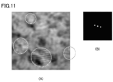
- FIGS. 10A and 11A show diffraction images of the high-resolution TEM image of FIG. 9, and FIGS. 10B and 11B show the diffraction patterns of FIGS. 10A and 11A.
- Fig. 4 shows imaging in different specific directions obtained by Fourier transform of a diffraction image.
- the crystal grain size when the crystal grain size was measured, the crystal grain size was 4 to 15 nm, and the average grain size was 7 nm.
- the crystal grain interval when the crystal grain interval was measured, it was 0 to 3 nm, and the average interval was 1 nm.
- thermoelectric characteristics were evaluated.
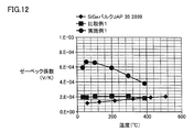
- FIG. 12 shows the measurement results of the Seebeck coefficient of the samples of Example 1 and Comparative Example 1 and Dismukes, JP, et al., (1964) J. App. Phys. 35, 2899-2907 (JAP 352899). It is a figure which shows the Seebeck coefficient of the bulk SiGe which is.
- the sample of Example 1 shows a high value near 0.7 mV / K, which is higher than that of bulk SiGe. This is understood to be the effect of having nanoparticles. Moreover, it is thought that it is the effect by the space
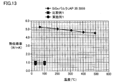
- FIG. 13 is a diagram showing the measurement results of the thermal conductivity of the samples of Example 1 and Comparative Example 1, and the thermal conductivity of bulk SiGe shown in JAP352899.
- the sample of Example 1 exhibited a low thermal conductivity of 1/5 or less compared to bulk SiGe. This is considered to be an effect due to the improvement of phonon scattering by having nanoparticles.
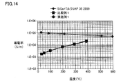
- FIG. 14 is a diagram showing the measurement results of the electrical conductivity of the samples of Example 1 and Comparative Example 1, and the electrical conductivity of bulk SiGe shown in JAP352899.
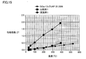
- FIG. 15 is a diagram showing the calculation result of the dimensionless figure of merit ZT of the samples of Example 1 and Comparative Example 1, and the dimensionless figure of merit ZT of bulk SiGe shown in JAPA352899. As shown in FIG. 15, the dimensionless figure of merit ZT of the sample of Example 1 was higher than that of the sample of Comparative Example 1 and bulk SiGe.
Landscapes
- Chemical & Material Sciences (AREA)
- Inorganic Chemistry (AREA)
- Engineering & Computer Science (AREA)
- Manufacturing & Machinery (AREA)
- Physical Vapour Deposition (AREA)
- Powder Metallurgy (AREA)
- Physical Deposition Of Substances That Are Components Of Semiconductor Devices (AREA)
Abstract
L'invention concerne un procédé de fabrication de nanoparticules selon lequel sont formées des nanoparticules contenant dans une matière de base constituée d'un matériau semi-conducteur configuré par un élément matière de base, cet élément matière de base et un élément différent distinct de l'élément matière de base. Le procédé de l'invention comporte : une étape de stratification au cours de laquelle une première couche (20) contenant l'élément différent, et une seconde couche (30) ne contenant pas l'élément différent, sont stratifiées l'une sur l'autre ; et une étape de recuit au cours de laquelle un traitement de recuit est appliqué au corps stratifié dans lequel la première et la seconde couche (20, 30) sont stratifiées, et les nanoparticules sont ainsi formées dans la matière de base. Au cours de l'étape de stratification, l'ensemble de l'élément matière de base est inclus dans la première couche (20) et/ou la seconde couche (30), et la seconde couche (30) est formée de sorte à être plus épaisse que la première couche (20).
Priority Applications (3)
| Application Number | Priority Date | Filing Date | Title |
|---|---|---|---|
| US14/895,266 US20160126440A1 (en) | 2013-06-04 | 2014-05-30 | Method of producing nanoparticles, method of producing thermoelectric material, and thermoelectric material |
| PCT/JP2014/064468 WO2014196475A1 (fr) | 2013-06-04 | 2014-05-30 | Procédé de fabrication de nanoparticules, et matériau thermoélectrique ainsi que procédé de fabrication de celui-ci |
| JP2015521431A JPWO2014196475A1 (ja) | 2013-06-04 | 2014-05-30 | ナノ粒子の製造方法、熱電材料の製造方法および熱電材料 |
Applications Claiming Priority (4)
| Application Number | Priority Date | Filing Date | Title |
|---|---|---|---|
| JP2013-117932 | 2013-06-04 | ||
| JP2013117932 | 2013-06-04 | ||
| JP2013226739 | 2013-10-31 | ||
| JP2013-226739 | 2013-10-31 |
Publications (1)
| Publication Number | Publication Date |
|---|---|
| WO2014196233A1 true WO2014196233A1 (fr) | 2014-12-11 |
Family
ID=52007889
Family Applications (2)
| Application Number | Title | Priority Date | Filing Date |
|---|---|---|---|
| PCT/JP2014/054868 Ceased WO2014196233A1 (fr) | 2013-06-04 | 2014-02-27 | Procédé de fabrication de nanoparticules, et matériau thermoélectrique ainsi que procédé de fabrication de celui-ci |
| PCT/JP2014/064468 Ceased WO2014196475A1 (fr) | 2013-06-04 | 2014-05-30 | Procédé de fabrication de nanoparticules, et matériau thermoélectrique ainsi que procédé de fabrication de celui-ci |
Family Applications After (1)
| Application Number | Title | Priority Date | Filing Date |
|---|---|---|---|
| PCT/JP2014/064468 Ceased WO2014196475A1 (fr) | 2013-06-04 | 2014-05-30 | Procédé de fabrication de nanoparticules, et matériau thermoélectrique ainsi que procédé de fabrication de celui-ci |
Country Status (4)
| Country | Link |
|---|---|
| US (1) | US20160126440A1 (fr) |
| JP (1) | JPWO2014196475A1 (fr) |
| TW (1) | TW201512077A (fr) |
| WO (2) | WO2014196233A1 (fr) |
Cited By (5)
| Publication number | Priority date | Publication date | Assignee | Title |
|---|---|---|---|---|
| JP2017050505A (ja) * | 2015-09-04 | 2017-03-09 | 株式会社日立製作所 | 熱電変換材料および熱電変換モジュール |
| JP2017212414A (ja) * | 2016-05-27 | 2017-11-30 | 大同特殊鋼株式会社 | ホイスラー型鉄系熱電材料 |
| JP2017216388A (ja) * | 2016-06-01 | 2017-12-07 | 住友電気工業株式会社 | 熱電材料、熱電素子、光センサおよび熱電材料の製造方法 |
| JPWO2017002514A1 (ja) * | 2015-06-30 | 2018-04-19 | 住友電気工業株式会社 | 熱電材料、熱電素子、光センサおよび熱電材料の製造方法 |
| JPWO2019244428A1 (ja) * | 2018-06-18 | 2021-07-15 | 住友電気工業株式会社 | 熱電変換材料、熱電変換素子、熱電変換モジュール、光センサおよび熱電変換材料の製造方法 |
Families Citing this family (7)
| Publication number | Priority date | Publication date | Assignee | Title |
|---|---|---|---|---|
| US20160315243A1 (en) * | 2015-04-22 | 2016-10-27 | The Regents Of The University Of California | Charged particle beam processing of thermoelectric materials |
| WO2018043478A1 (fr) * | 2016-08-31 | 2018-03-08 | 住友電気工業株式会社 | Matériau de conversion thermoélectrique, élément de conversion thermoélectrique et module de conversion thermoélectrique |
| JP6768556B2 (ja) * | 2017-02-27 | 2020-10-14 | 株式会社日立製作所 | 熱電変換材料及びその製造方法 |
| WO2019180999A1 (fr) | 2018-03-20 | 2019-09-26 | 住友電気工業株式会社 | Matériau de conversion thermoélectrique, élément de conversion thermoélectrique, module de conversion thermoélectrique et capteur de lumière |
| JP7597579B2 (ja) | 2018-09-03 | 2024-12-10 | 住友電気工業株式会社 | 熱電変換素子、熱電変換モジュール、光センサ、熱電変換材料の製造方法および熱電変換素子の製造方法 |
| WO2021002221A1 (fr) | 2019-07-03 | 2021-01-07 | 住友電気工業株式会社 | Matériau de conversion thermoélectrique, élément de conversion thermoélectrique, module de conversion thermoélectrique et capteur de lumière |
| CN119400310B (zh) * | 2024-10-15 | 2026-02-13 | 山东大学深圳研究院 | 一种纳米层状结构材料制备过程的模拟方法、应用和系统 |
Citations (3)
| Publication number | Priority date | Publication date | Assignee | Title |
|---|---|---|---|---|
| JPH10242535A (ja) * | 1997-02-27 | 1998-09-11 | Central Res Inst Of Electric Power Ind | 熱電材料及びその製造方法 |
| US20080001127A1 (en) * | 2006-06-19 | 2008-01-03 | The Regents Of The University Of California | High efficiency thermoelectric materials based on metal/semiconductor nanocomposites |
| WO2012026678A2 (fr) * | 2010-08-26 | 2012-03-01 | Lg Innotek Co., Ltd. | Module thermoélectrique comprenant un élément thermoélectrique dopé par des nanoparticules et son procédé de fabrication |
Family Cites Families (2)
| Publication number | Priority date | Publication date | Assignee | Title |
|---|---|---|---|---|
| US7465871B2 (en) * | 2004-10-29 | 2008-12-16 | Massachusetts Institute Of Technology | Nanocomposites with high thermoelectric figures of merit |
| WO2011037794A2 (fr) * | 2009-09-25 | 2011-03-31 | Northwestern University | Compositions thermoélectriques comprenant des inclusions nanométriques dans une matrice chalcogénure |
-
2014
- 2014-02-27 WO PCT/JP2014/054868 patent/WO2014196233A1/fr not_active Ceased
- 2014-05-30 JP JP2015521431A patent/JPWO2014196475A1/ja active Pending
- 2014-05-30 WO PCT/JP2014/064468 patent/WO2014196475A1/fr not_active Ceased
- 2014-05-30 US US14/895,266 patent/US20160126440A1/en not_active Abandoned
- 2014-06-04 TW TW103119432A patent/TW201512077A/zh unknown
Patent Citations (3)
| Publication number | Priority date | Publication date | Assignee | Title |
|---|---|---|---|---|
| JPH10242535A (ja) * | 1997-02-27 | 1998-09-11 | Central Res Inst Of Electric Power Ind | 熱電材料及びその製造方法 |
| US20080001127A1 (en) * | 2006-06-19 | 2008-01-03 | The Regents Of The University Of California | High efficiency thermoelectric materials based on metal/semiconductor nanocomposites |
| WO2012026678A2 (fr) * | 2010-08-26 | 2012-03-01 | Lg Innotek Co., Ltd. | Module thermoélectrique comprenant un élément thermoélectrique dopé par des nanoparticules et son procédé de fabrication |
Cited By (6)
| Publication number | Priority date | Publication date | Assignee | Title |
|---|---|---|---|---|
| JPWO2017002514A1 (ja) * | 2015-06-30 | 2018-04-19 | 住友電気工業株式会社 | 熱電材料、熱電素子、光センサおよび熱電材料の製造方法 |
| JP2017050505A (ja) * | 2015-09-04 | 2017-03-09 | 株式会社日立製作所 | 熱電変換材料および熱電変換モジュール |
| JP2017212414A (ja) * | 2016-05-27 | 2017-11-30 | 大同特殊鋼株式会社 | ホイスラー型鉄系熱電材料 |
| JP2017216388A (ja) * | 2016-06-01 | 2017-12-07 | 住友電気工業株式会社 | 熱電材料、熱電素子、光センサおよび熱電材料の製造方法 |
| JPWO2019244428A1 (ja) * | 2018-06-18 | 2021-07-15 | 住友電気工業株式会社 | 熱電変換材料、熱電変換素子、熱電変換モジュール、光センサおよび熱電変換材料の製造方法 |
| JP7296377B2 (ja) | 2018-06-18 | 2023-06-22 | 住友電気工業株式会社 | 熱電変換材料、熱電変換素子、熱電変換モジュール、光センサおよび熱電変換材料の製造方法 |
Also Published As
| Publication number | Publication date |
|---|---|
| WO2014196475A1 (fr) | 2014-12-11 |
| US20160126440A1 (en) | 2016-05-05 |
| JPWO2014196475A1 (ja) | 2017-02-23 |
| TW201512077A (zh) | 2015-04-01 |
Similar Documents
| Publication | Publication Date | Title |
|---|---|---|
| WO2014196233A1 (fr) | Procédé de fabrication de nanoparticules, et matériau thermoélectrique ainsi que procédé de fabrication de celui-ci | |
| Yang et al. | Enhanced thermoelectric properties in bulk nanowire heterostructure-based nanocomposites through minority carrier blocking | |
| JP6269352B2 (ja) | 熱電材料、熱電モジュール、光センサおよび熱電材料の製造方法 | |
| Andrews et al. | Atomic-level control of the thermoelectric properties in polytypoid nanowires | |
| Tan et al. | Ordered structure and high thermoelectric properties of Bi2 (Te, Se) 3 nanowire array | |
| JP6927039B2 (ja) | 熱電材料、熱電素子、光センサおよび熱電材料の製造方法 | |
| CN102791905B (zh) | 溅射靶及其制造方法、以及半导体元件的制造方法 | |
| Park et al. | Effect of grain size on thermal transport in post-annealed antimony telluride thin films | |
| Xin et al. | Improving the thermoelectric performance of Cu-doped MoS2 film by band structure modification and microstructural regulation | |
| Lee et al. | Design and preparation of high-performance bulk thermoelectric materials with defect structures | |
| KR20110041214A (ko) | 코어/쉘 구조를 갖는 열전 나노와이어의 제조방법 | |
| Ao et al. | Texture and Se vacancy optimization induces high thermoelectric performance in Bi2Se3 flexible thin films | |
| Lee et al. | Effect of electronic contribution on temperature-dependent thermal transport of antimony telluride thin film | |
| Ko et al. | Intense near-infrared emission from undoped ZnTe nanostructures synthesized by thermal evaporation | |
| CN109219894B (zh) | 热电材料、热电元件、光学传感器和热电材料的制造方法 | |
| Bae et al. | Growth of ZnO nanorod arrays by hydrothermal method using homo‐seed layers annealed at various temperatures | |
| Abd Rahim et al. | Self-assembled Ge islands and nanocrystals by RF magnetron sputtering and rapid thermal processing: The role of annealing temperature | |
| WO2012005423A1 (fr) | Nanofil thermoélectrique hétérostructuré et son procédé de fabrication same | |
| Qin et al. | Effect of oxidation condition on growth of N: ZnO prepared by oxidizing sputtering Zn-N film | |
| Conley et al. | Stability of pseudomorphic and compressively strained Ge1-xSnx thin films under rapid thermal annealing | |
| Winkler et al. | Sputtered n-type Bi2Te3/(Bi, Sb) 2Te3 superlattice systems | |
| Gharleghi et al. | Enhancing the Thermoelectric Performance of Hydrothermally Synthesized Porous n-Type Co4–y–z Ni y Fe z Sb12 Skutterudites via Solid–Vapor Indium Incorporation | |
| Takagaki et al. | Overgrowth of Bi 2 Te 3 nanoislands on Fe-based epitaxial ferromagnetic layers | |
| KR101726498B1 (ko) | 고망간실리사이드계 화합물을 포함하는 열전소재 및 이의 제조방법 | |
| Ali | Synthesis, Processing, and Characterization of Magnesium-Based Thermoelectric Materials |
Legal Events
| Date | Code | Title | Description |
|---|---|---|---|
| 121 | Ep: the epo has been informed by wipo that ep was designated in this application |
Ref document number: 14808274 Country of ref document: EP Kind code of ref document: A1 |
|
| NENP | Non-entry into the national phase |
Ref country code: DE |
|
| 122 | Ep: pct application non-entry in european phase |
Ref document number: 14808274 Country of ref document: EP Kind code of ref document: A1 |