WO2014203348A1 - Cu核ボール - Google Patents
Cu核ボール Download PDFInfo
- Publication number
- WO2014203348A1 WO2014203348A1 PCT/JP2013/066827 JP2013066827W WO2014203348A1 WO 2014203348 A1 WO2014203348 A1 WO 2014203348A1 JP 2013066827 W JP2013066827 W JP 2013066827W WO 2014203348 A1 WO2014203348 A1 WO 2014203348A1
- Authority
- WO
- WIPO (PCT)
- Prior art keywords
- ball
- solder
- dose
- core
- plating film
- Prior art date
- Legal status (The legal status is an assumption and is not a legal conclusion. Google has not performed a legal analysis and makes no representation as to the accuracy of the status listed.)
- Ceased
Links
Images


Classifications
-
- C—CHEMISTRY; METALLURGY
- C22—METALLURGY; FERROUS OR NON-FERROUS ALLOYS; TREATMENT OF ALLOYS OR NON-FERROUS METALS
- C22C—ALLOYS
- C22C13/00—Alloys based on tin
-
- B—PERFORMING OPERATIONS; TRANSPORTING
- B22—CASTING; POWDER METALLURGY
- B22F—WORKING METALLIC POWDER; MANUFACTURE OF ARTICLES FROM METALLIC POWDER; MAKING METALLIC POWDER; APPARATUS OR DEVICES SPECIALLY ADAPTED FOR METALLIC POWDER
- B22F1/00—Metallic powder; Treatment of metallic powder, e.g. to facilitate working or to improve properties
- B22F1/17—Metallic particles coated with metal
-
- B—PERFORMING OPERATIONS; TRANSPORTING
- B23—MACHINE TOOLS; METAL-WORKING NOT OTHERWISE PROVIDED FOR
- B23K—SOLDERING OR UNSOLDERING; WELDING; CLADDING OR PLATING BY SOLDERING OR WELDING; CUTTING BY APPLYING HEAT LOCALLY, e.g. FLAME CUTTING; WORKING BY LASER BEAM
- B23K35/00—Rods, electrodes, materials, or media, for use in soldering, welding, or cutting
- B23K35/02—Rods, electrodes, materials, or media, for use in soldering, welding, or cutting characterised by mechanical features, e.g. shape
- B23K35/0222—Rods, electrodes, materials, or media, for use in soldering, welding, or cutting characterised by mechanical features, e.g. shape for use in soldering or brazing
- B23K35/0244—Powders, particles or spheres; Preforms made therefrom
-
- B—PERFORMING OPERATIONS; TRANSPORTING
- B23—MACHINE TOOLS; METAL-WORKING NOT OTHERWISE PROVIDED FOR
- B23K—SOLDERING OR UNSOLDERING; WELDING; CLADDING OR PLATING BY SOLDERING OR WELDING; CUTTING BY APPLYING HEAT LOCALLY, e.g. FLAME CUTTING; WORKING BY LASER BEAM
- B23K35/00—Rods, electrodes, materials, or media, for use in soldering, welding, or cutting
- B23K35/22—Rods, electrodes, materials, or media, for use in soldering, welding, or cutting characterised by the composition or nature of the material
- B23K35/24—Selection of soldering or welding materials proper
- B23K35/26—Selection of soldering or welding materials proper with the principal constituent melting at less than 400°C
-
- B—PERFORMING OPERATIONS; TRANSPORTING
- B23—MACHINE TOOLS; METAL-WORKING NOT OTHERWISE PROVIDED FOR
- B23K—SOLDERING OR UNSOLDERING; WELDING; CLADDING OR PLATING BY SOLDERING OR WELDING; CUTTING BY APPLYING HEAT LOCALLY, e.g. FLAME CUTTING; WORKING BY LASER BEAM
- B23K35/00—Rods, electrodes, materials, or media, for use in soldering, welding, or cutting
- B23K35/22—Rods, electrodes, materials, or media, for use in soldering, welding, or cutting characterised by the composition or nature of the material
- B23K35/24—Selection of soldering or welding materials proper
- B23K35/26—Selection of soldering or welding materials proper with the principal constituent melting at less than 400°C
- B23K35/262—Sn as the principal constituent
-
- B—PERFORMING OPERATIONS; TRANSPORTING
- B23—MACHINE TOOLS; METAL-WORKING NOT OTHERWISE PROVIDED FOR
- B23K—SOLDERING OR UNSOLDERING; WELDING; CLADDING OR PLATING BY SOLDERING OR WELDING; CUTTING BY APPLYING HEAT LOCALLY, e.g. FLAME CUTTING; WORKING BY LASER BEAM
- B23K35/00—Rods, electrodes, materials, or media, for use in soldering, welding, or cutting
- B23K35/22—Rods, electrodes, materials, or media, for use in soldering, welding, or cutting characterised by the composition or nature of the material
- B23K35/24—Selection of soldering or welding materials proper
- B23K35/30—Selection of soldering or welding materials proper with the principal constituent melting at less than 1550°C
-
- B—PERFORMING OPERATIONS; TRANSPORTING
- B23—MACHINE TOOLS; METAL-WORKING NOT OTHERWISE PROVIDED FOR
- B23K—SOLDERING OR UNSOLDERING; WELDING; CLADDING OR PLATING BY SOLDERING OR WELDING; CUTTING BY APPLYING HEAT LOCALLY, e.g. FLAME CUTTING; WORKING BY LASER BEAM
- B23K35/00—Rods, electrodes, materials, or media, for use in soldering, welding, or cutting
- B23K35/22—Rods, electrodes, materials, or media, for use in soldering, welding, or cutting characterised by the composition or nature of the material
- B23K35/24—Selection of soldering or welding materials proper
- B23K35/30—Selection of soldering or welding materials proper with the principal constituent melting at less than 1550°C
- B23K35/302—Cu as the principal constituent
-
- C—CHEMISTRY; METALLURGY
- C22—METALLURGY; FERROUS OR NON-FERROUS ALLOYS; TREATMENT OF ALLOYS OR NON-FERROUS METALS
- C22C—ALLOYS
- C22C43/00—Alloys containing radioactive materials
-
- C—CHEMISTRY; METALLURGY
- C22—METALLURGY; FERROUS OR NON-FERROUS ALLOYS; TREATMENT OF ALLOYS OR NON-FERROUS METALS
- C22C—ALLOYS
- C22C9/00—Alloys based on copper
-
- C—CHEMISTRY; METALLURGY
- C23—COATING METALLIC MATERIAL; COATING MATERIAL WITH METALLIC MATERIAL; CHEMICAL SURFACE TREATMENT; DIFFUSION TREATMENT OF METALLIC MATERIAL; COATING BY VACUUM EVAPORATION, BY SPUTTERING, BY ION IMPLANTATION OR BY CHEMICAL VAPOUR DEPOSITION, IN GENERAL; INHIBITING CORROSION OF METALLIC MATERIAL OR INCRUSTATION IN GENERAL
- C23C—COATING METALLIC MATERIAL; COATING MATERIAL WITH METALLIC MATERIAL; SURFACE TREATMENT OF METALLIC MATERIAL BY DIFFUSION INTO THE SURFACE, BY CHEMICAL CONVERSION OR SUBSTITUTION; COATING BY VACUUM EVAPORATION, BY SPUTTERING, BY ION IMPLANTATION OR BY CHEMICAL VAPOUR DEPOSITION, IN GENERAL
- C23C28/00—Coating for obtaining at least two superposed coatings either by methods not provided for in a single one of groups C23C2/00 - C23C26/00 or by combinations of methods provided for in subclasses C23C and C25C or C25D
- C23C28/02—Coating for obtaining at least two superposed coatings either by methods not provided for in a single one of groups C23C2/00 - C23C26/00 or by combinations of methods provided for in subclasses C23C and C25C or C25D only coatings only including layers of metallic material
- C23C28/021—Coating for obtaining at least two superposed coatings either by methods not provided for in a single one of groups C23C2/00 - C23C26/00 or by combinations of methods provided for in subclasses C23C and C25C or C25D only coatings only including layers of metallic material including at least one metal alloy layer
-
- H—ELECTRICITY
- H10—SEMICONDUCTOR DEVICES; ELECTRIC SOLID-STATE DEVICES NOT OTHERWISE PROVIDED FOR
- H10W—GENERIC PACKAGES, INTERCONNECTIONS, CONNECTORS OR OTHER CONSTRUCTIONAL DETAILS OF DEVICES COVERED BY CLASS H10
- H10W42/00—Arrangements for protection of devices
- H10W42/20—Arrangements for protection of devices protecting against electromagnetic or particle radiation, e.g. light, X-rays, gamma-rays or electrons
- H10W42/25—Arrangements for protection of devices protecting against electromagnetic or particle radiation, e.g. light, X-rays, gamma-rays or electrons against alpha rays, e.g. for outer space applications
-
- H—ELECTRICITY
- H10—SEMICONDUCTOR DEVICES; ELECTRIC SOLID-STATE DEVICES NOT OTHERWISE PROVIDED FOR
- H10W—GENERIC PACKAGES, INTERCONNECTIONS, CONNECTORS OR OTHER CONSTRUCTIONAL DETAILS OF DEVICES COVERED BY CLASS H10
- H10W72/00—Interconnections or connectors in packages
- H10W72/20—Bump connectors, e.g. solder bumps or copper pillars; Dummy bumps; Thermal bumps
-
- H—ELECTRICITY
- H10—SEMICONDUCTOR DEVICES; ELECTRIC SOLID-STATE DEVICES NOT OTHERWISE PROVIDED FOR
- H10W—GENERIC PACKAGES, INTERCONNECTIONS, CONNECTORS OR OTHER CONSTRUCTIONAL DETAILS OF DEVICES COVERED BY CLASS H10
- H10W90/00—Package configurations
- H10W90/701—Package configurations characterised by the relative positions of pads or connectors relative to package parts
-
- H—ELECTRICITY
- H05—ELECTRIC TECHNIQUES NOT OTHERWISE PROVIDED FOR
- H05K—PRINTED CIRCUITS; CASINGS OR CONSTRUCTIONAL DETAILS OF ELECTRIC APPARATUS; MANUFACTURE OF ASSEMBLAGES OF ELECTRICAL COMPONENTS
- H05K2203/00—Indexing scheme relating to apparatus or processes for manufacturing printed circuits covered by H05K3/00
- H05K2203/04—Soldering or other types of metallurgic bonding
- H05K2203/041—Solder preforms in the shape of solder balls
-
- H—ELECTRICITY
- H05—ELECTRIC TECHNIQUES NOT OTHERWISE PROVIDED FOR
- H05K—PRINTED CIRCUITS; CASINGS OR CONSTRUCTIONAL DETAILS OF ELECTRIC APPARATUS; MANUFACTURE OF ASSEMBLAGES OF ELECTRICAL COMPONENTS
- H05K3/00—Apparatus or processes for manufacturing printed circuits
- H05K3/30—Assembling printed circuits with electric components, e.g. with resistors
- H05K3/32—Assembling printed circuits with electric components, e.g. with resistors electrically connecting electric components or wires to printed circuits
- H05K3/34—Assembling printed circuits with electric components, e.g. with resistors electrically connecting electric components or wires to printed circuits by soldering
- H05K3/3465—Application of solder
-
- H—ELECTRICITY
- H10—SEMICONDUCTOR DEVICES; ELECTRIC SOLID-STATE DEVICES NOT OTHERWISE PROVIDED FOR
- H10W—GENERIC PACKAGES, INTERCONNECTIONS, CONNECTORS OR OTHER CONSTRUCTIONAL DETAILS OF DEVICES COVERED BY CLASS H10
- H10W72/00—Interconnections or connectors in packages
- H10W72/01—Manufacture or treatment
- H10W72/012—Manufacture or treatment of bump connectors, dummy bumps or thermal bumps
- H10W72/01212—Manufacture or treatment of bump connectors, dummy bumps or thermal bumps at a different location than on the final device, e.g. forming as prepeg
-
- H—ELECTRICITY
- H10—SEMICONDUCTOR DEVICES; ELECTRIC SOLID-STATE DEVICES NOT OTHERWISE PROVIDED FOR
- H10W—GENERIC PACKAGES, INTERCONNECTIONS, CONNECTORS OR OTHER CONSTRUCTIONAL DETAILS OF DEVICES COVERED BY CLASS H10
- H10W72/00—Interconnections or connectors in packages
- H10W72/20—Bump connectors, e.g. solder bumps or copper pillars; Dummy bumps; Thermal bumps
- H10W72/221—Structures or relative sizes
- H10W72/225—Bumps having a filler embedded in a matrix
-
- H—ELECTRICITY
- H10—SEMICONDUCTOR DEVICES; ELECTRIC SOLID-STATE DEVICES NOT OTHERWISE PROVIDED FOR
- H10W—GENERIC PACKAGES, INTERCONNECTIONS, CONNECTORS OR OTHER CONSTRUCTIONAL DETAILS OF DEVICES COVERED BY CLASS H10
- H10W72/00—Interconnections or connectors in packages
- H10W72/20—Bump connectors, e.g. solder bumps or copper pillars; Dummy bumps; Thermal bumps
- H10W72/231—Shapes
- H10W72/232—Plan-view shape, i.e. in top view
-
- H—ELECTRICITY
- H10—SEMICONDUCTOR DEVICES; ELECTRIC SOLID-STATE DEVICES NOT OTHERWISE PROVIDED FOR
- H10W—GENERIC PACKAGES, INTERCONNECTIONS, CONNECTORS OR OTHER CONSTRUCTIONAL DETAILS OF DEVICES COVERED BY CLASS H10
- H10W72/00—Interconnections or connectors in packages
- H10W72/20—Bump connectors, e.g. solder bumps or copper pillars; Dummy bumps; Thermal bumps
- H10W72/231—Shapes
- H10W72/234—Cross-sectional shape, i.e. in side view
-
- H—ELECTRICITY
- H10—SEMICONDUCTOR DEVICES; ELECTRIC SOLID-STATE DEVICES NOT OTHERWISE PROVIDED FOR
- H10W—GENERIC PACKAGES, INTERCONNECTIONS, CONNECTORS OR OTHER CONSTRUCTIONAL DETAILS OF DEVICES COVERED BY CLASS H10
- H10W72/00—Interconnections or connectors in packages
- H10W72/20—Bump connectors, e.g. solder bumps or copper pillars; Dummy bumps; Thermal bumps
- H10W72/251—Materials
- H10W72/252—Materials comprising solid metals or solid metalloids, e.g. PbSn, Ag or Cu
-
- H—ELECTRICITY
- H10—SEMICONDUCTOR DEVICES; ELECTRIC SOLID-STATE DEVICES NOT OTHERWISE PROVIDED FOR
- H10W—GENERIC PACKAGES, INTERCONNECTIONS, CONNECTORS OR OTHER CONSTRUCTIONAL DETAILS OF DEVICES COVERED BY CLASS H10
- H10W72/00—Interconnections or connectors in packages
- H10W72/20—Bump connectors, e.g. solder bumps or copper pillars; Dummy bumps; Thermal bumps
- H10W72/251—Materials
- H10W72/255—Materials of outermost layers of multilayered bumps, e.g. material of a coating
-
- H—ELECTRICITY
- H10—SEMICONDUCTOR DEVICES; ELECTRIC SOLID-STATE DEVICES NOT OTHERWISE PROVIDED FOR
- H10W—GENERIC PACKAGES, INTERCONNECTIONS, CONNECTORS OR OTHER CONSTRUCTIONAL DETAILS OF DEVICES COVERED BY CLASS H10
- H10W90/00—Package configurations
- H10W90/701—Package configurations characterised by the relative positions of pads or connectors relative to package parts
- H10W90/721—Package configurations characterised by the relative positions of pads or connectors relative to package parts of bump connectors
- H10W90/722—Package configurations characterised by the relative positions of pads or connectors relative to package parts of bump connectors between stacked chips
-
- H—ELECTRICITY
- H10—SEMICONDUCTOR DEVICES; ELECTRIC SOLID-STATE DEVICES NOT OTHERWISE PROVIDED FOR
- H10W—GENERIC PACKAGES, INTERCONNECTIONS, CONNECTORS OR OTHER CONSTRUCTIONAL DETAILS OF DEVICES COVERED BY CLASS H10
- H10W90/00—Package configurations
- H10W90/701—Package configurations characterised by the relative positions of pads or connectors relative to package parts
- H10W90/721—Package configurations characterised by the relative positions of pads or connectors relative to package parts of bump connectors
- H10W90/724—Package configurations characterised by the relative positions of pads or connectors relative to package parts of bump connectors between a chip and a stacked insulating package substrate, interposer or RDL
Definitions
- the present invention relates to a Cu core ball having a low ⁇ dose.
- the electronic components to be mounted have been rapidly downsized.
- the electronic component uses a ball grid array (hereinafter referred to as “BGA”) in which electrodes are provided on the back surface. .
- BGA ball grid array
- An electronic component to which BGA is applied includes, for example, a semiconductor package.
- a semiconductor package a semiconductor chip having electrodes is sealed with a resin.
- Solder bumps are formed on the electrodes of the semiconductor chip. This solder bump is formed by joining a solder ball to an electrode of a semiconductor chip.
- a semiconductor package to which BGA is applied is mounted on a printed circuit board by bonding solder bumps melted by heating and conductive lands of the printed circuit board. Further, in order to meet the demand for further high-density mounting, three-dimensional high-density mounting in which semiconductor packages are stacked in the height direction has been studied.
- the solder ball when BGA is applied to a semiconductor package on which three-dimensional high-density mounting is performed, the solder ball may be crushed by the weight of the semiconductor package. If such a thing occurs, the solder may protrude from the electrodes, the electrodes may be connected, and a short circuit may occur.
- solder bumps made of Cu core balls bonded to the electrodes of electronic components are being studied.
- the Cu core ball is a product in which a solder coating is formed on the surface of the Cu ball.
- Solder bumps formed using Cu core balls support the semiconductor package with Cu balls that do not melt at the melting point of the solder, even when the weight of the semiconductor package is added to the solder bump when an electronic component is mounted on a printed circuit board. Can do. Therefore, the solder bump is not crushed by the weight of the semiconductor package.
- Patent Document 1 is cited as a related technique.
- Patent Document 1 discloses an invention of a Cu ball having a high sphericity, and also describes a Cu core ball in which a solder coating is formed on the Cu ball.
- This document exemplifies a Pb—Sn solder whose constituent elements are Pb and Sn.
- a plating method, a welding method, a brazing method, and the like are disclosed as equivalent methods as a method for forming a film.
- electrolytic plating methods such as barrel plating are disclosed as plating methods.
- Patent Document 2 discloses an invention of a Sn ingot with a low ⁇ dose, and in order to reduce the ⁇ dose, Pb and Bi are not suspended by simply suspending an adsorbent in the electrolytic solution instead of simply performing electrolytic refining. Is adsorbed to reduce the ⁇ dose.
- An object of the present invention is to provide a Cu core ball that suppresses the occurrence of a soft error, and specifically, to provide a Cu core ball with a low ⁇ dose.
- Patent Document 1 does not consider any problem of reducing the ⁇ dose of the Cu core ball.
- Pb—Sn alloy is disclosed as an explanation of the background art regarding the solder alloy constituting the solder coating.
- the ⁇ ray is emitted from 210 Po in the process in which the Pb isotope 210 Pb contained as an impurity in Sn decays from 210 Pb ⁇ 210 Bi ⁇ 210 Po ⁇ 206 Pb.
- the Pb—Sn solder alloy disclosed only in this document contains a large amount of Pb, it is considered that it also contains 210 Pb which is a radioactive element. Therefore, even if this solder alloy is applied to the solder coating of a Cu core ball, the problem of reducing the ⁇ dose is not considered in Patent Document 1, so the Cu core ball disclosed in the same document has a low ⁇ It is unlikely to show a dose.
- Patent Document 2 describes that, as described above, Pb and Bi in the Sn ingot are removed to reduce the ⁇ dose by electrolytic refining performed in a state where the electrolytic solution and the electrode are stationary.
- the same document does not disclose at all about performing Sn plating on a Cu ball or performing electrolytic plating in a state where the Cu ball and the electrolyte flow.
- the electrolytic refining described in the same document since the electrolytic deposition surface is limited to one direction, it is not possible to form a plating having a uniform film thickness on a micro work such as a Cu ball.
- Patent Document 2 since Pb and Bi have a standard electrode potential close to that of Sn, it is difficult to reduce the ⁇ dose only by performing electrolytic deposition of Sn on a plate electrode by general electrolytic refining. If the electrolytic refining described in Patent Document 2 is applied to the formation of a plating film of Cu balls, and the barrel plating is performed by suspending the adsorbent in the plating solution, the plating solution and the workpiece are stirred, and the adsorbent is also stirred at the same time. Is done. In this case, Pb ions and Bi ions adsorbed on the adsorbent may become carriers and be taken into the solder coating together with the adsorbent.
- the solder film that has absorbed the adsorbent emits high alpha rays. Further, since the particle size of the adsorbent is about submicron and very small, it is considered difficult to separate and collect the adsorbent after suspension while flowing the plating solution. Therefore, it is difficult to prevent the adsorbent that has adsorbed Pb and Bi from being taken into the film.
- Patent Document 1 Pb—Sn solder alloy is disclosed in Patent Document 1, but since the plating method, welding method, brazing method, and the like are disclosed as equivalent methods, rather, the ⁇ dose can be reduced. It is written that denial.
- the subject of patent document 1 is in manufacturing Cu core ball with high sphericity.
- Patent Document 2 discloses that Pb in Sn is removed as much as possible by electrolytic refining in order to solve the problem of reducing the ⁇ dose.
- Patent Document 1 will not recall the problem of reducing the ⁇ dose of Cu core balls disclosed in Patent Document 2, and the composition of the solder is also in conflict, so the ⁇ dose is In order to recall the problem to be reduced, and to come up with the application of Sn-based solder from among a myriad of solder alloys instead of the Pb—Sn solder alloy constituting the solder coating, it is limited to a few Considered no trial and error.
- Patent Document 1 Even those skilled in the art cannot combine Patent Document 1 and Patent Document 2. Furthermore, even a person skilled in the art forms a plating solution using a Sn ingot disclosed in Patent Document 2 with a low ⁇ dose and forms a Cu core ball by the plating method disclosed in Patent Document 1. It is also very difficult to do.
- the radioactive element present in the solder coating of the Cu core ball is the joint element.
- ⁇ rays are emitted by diffusing to the electrode. Therefore, even if the conventional techniques are combined, the ⁇ dose of the Cu core ball cannot be reduced, and thus it is impossible to avoid a soft error that has become a new problem due to high-density mounting.
- the inventors first selected a Cu ball to be used for the Cu core ball. As a result, if a certain amount of Pb and / or Bi is not contained in the Cu ball, the sphericity of the Cu ball decreases, and the solder plating on the Cu ball does not become uniform when performing solder plating. It was found that the sphericity of the resulting Cu core ball is reduced. Next, in order to reduce the ⁇ dose of the solder coating constituting the Cu core ball, intensive studies were conducted focusing on the point of forming the solder plating coating using a plating method.
- the present inventors have formed a plating film on the Cu ball while flowing the Cu ball or the plating solution.
- these Pb, Bi and Po elements formed salts without suspending the adsorbent. And since this salt is electrically neutral, these elements were not taken in into a plating film, and the knowledge that the alpha dose of the plating film which comprises a Cu core ball decreased was acquired.
- a Cu core ball comprising a Cu ball and a solder plating film covering the surface of the Cu ball
- the solder plating film is an Sn solder plating film or a solder plating film made of a lead-free solder alloy containing Sn as a main component, the U content is 5 ppb or less, and the Th content is 5 ppb or less.
- the purity of the Cu balls is 99.9% or more and 99.995% or less, the total content of Pb and / or Bi is 1 ppm or more, the sphericity is 0.95 or more, and the Cu core balls
- solder plating film constituting the present invention includes a Sn solder plating film.
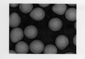
- FIG. 1 is an SEM photograph of Cu balls manufactured using Cu pellets having a purity of 99.9%.
- FIG. 2 is an SEM photograph of a Cu ball manufactured using a Cu wire having a purity of 99.995% or less.
- FIG. 3 is a SEM photograph of a Cu ball manufactured using a Cu plate having a purity exceeding 99.995%.
- the unit (ppm, ppb, and%) related to the composition of the solder coating of the Cu core ball represents a ratio (mass ppm, mass ppb, and mass%) to the mass of the solder coating unless otherwise specified.
- the units (ppm, ppb, and%) relating to the composition of the Cu balls represent ratios (mass ppm, mass ppb, and mass%) with respect to the mass of the Cu balls unless otherwise specified.
- the Cu core ball according to the present invention includes a Cu ball and a solder plating film that covers the surface of the Cu ball.
- the solder plating film of the present invention is formed mainly by flowing a Cu ball or a plating solution as a work. Due to the flow of the plating solution, elements of Pb, Bi, and Po form salts in the plating solution and precipitate. Once a precipitate that is a salt is formed, it is stably present in the plating solution. Therefore, in the Cu core ball according to the present invention, no precipitate is taken into the solder coating, the content of radioactive elements contained in the solder coating can be reduced, and the ⁇ dose of the Cu core ball itself can be reduced. Become. Below, the solder plating film and Cu ball
- solder plating film-Composition of solder plating film is not particularly limited as long as it is an alloy composition of a lead-free solder alloy containing Sn as a main component.
- the solder plating film may be a Sn plating film. Examples thereof include Sn, Sn—Ag alloy, Sn—Cu alloy, Sn—Ag—Cu alloy, Sn—In alloy, and those obtained by adding a predetermined alloy element thereto. In any case, the Sn content is 40% by mass or more.
- alloy elements to be added include Ag, Cu, In, Ni, Co, Sb, Ge, P, and Fe.
- the alloy composition of the solder plating film is preferably a Sn-3Ag-0.5Cu alloy from the viewpoint of drop impact characteristics.
- the thickness of the solder plating film is not particularly limited, but is preferably 100 ⁇ m (one side) or less. Generally, it may be 20 to 50 ⁇ m.
- U and Th are radioactive elements, and it is necessary to suppress their contents in order to suppress soft errors.
- the contents of U and Th are required to be 5 ppb or less in order to set the ⁇ dose of the solder plating film to 0.0200 cph / cm 2 or less. Further, from the viewpoint of suppressing soft errors in current or future high-density mounting, the contents of U and Th are preferably 2 ppb or less, respectively.
- the ⁇ dose of the Cu core ball according to the present invention is 0.0200 cph / cm 2 or less. This is an ⁇ dose that does not cause a soft error in high-density mounting of electronic components.
- the ⁇ dose of the Cu core ball according to the present invention is achieved when the ⁇ dose of the solder plating film constituting the Cu core ball is 0.0200 cph / cm 2 or less. Since the solder plating film of the present invention is formed at a temperature of 100 ° C. at the highest, it is unlikely that the content of radioactive elements is reduced by vaporization of radioactive elements such as U, Th, 210 Po, Bi and Pb.
- the Cu core ball according to the present invention is coated with such a solder plating film, it exhibits a low ⁇ dose.
- the ⁇ dose is preferably 0.0020 cph / cm 2 or less, more preferably 0.0010 cph / cm 2 or less, from the viewpoint of suppressing soft errors in further high-density mounting.
- the upper limit is preferably 150 ppm or less, more preferably 100 ppm or less, still more preferably 50 ppm or less, and particularly preferably 10 ppm or less from the viewpoint of reducing the ⁇ dose.
- the purity of the solder plating film is the total content of impurities other than Sn in the solder plating film.
- the solder plating film is a Sn-3Ag-0.5Cu solder alloy
- the purity of the solder plating film is the sum of the contents of impurities other than Sn, Ag and Cu in the solder plating film.
- the impurities contained in the solder plating film include Ag, Ni, Pb, Au, U, and Th in the case of the Sn solder plating film.
- Sb, Fe, As, In, Ni, Pb, Au, U, Th and the like can be mentioned.
- the Bi content is small.
- Bi raw materials contain a trace amount of 210 Bi, which is a radioisotope. Therefore, it is considered that the ⁇ dose of the solder plating film can be remarkably reduced by reducing the Bi content.
- the Bi content is preferably 15 ppm or less, more preferably 10 ppm or less, and particularly preferably 0 ppm.
- the Cu ball constituting the present invention does not melt at the soldering temperature when the Cu core ball is used for a solder bump, the height variation of the solder joint can be suppressed. Therefore, it is preferable that the Cu ball has a high sphericity and a small variation in diameter. Further, as described above, it is preferable that the ⁇ dose of the Cu ball is low as well as the solder coating.
- the preferred embodiment of the Cu ball is described below. -Purity of Cu ball: 99.9% or more and 99.995% or less
- the Cu ball constituting the present invention preferably has a purity of 99.9% or more and 99.995% or less.
- the Cu material formed into small pieces of a predetermined shape is melted by heating, and the molten Cu becomes spherical due to surface tension, which solidifies into a Cu ball.
- the molten Cu solidifies from the liquid state, crystal grains grow in the spherical molten Cu.
- the impurity elements serve as crystal nuclei and growth of crystal grains is suppressed. Therefore, the spherical molten Cu becomes a Cu ball having a high sphericity due to the fine crystal grains whose growth is suppressed.
- the impurity element Sn, Sb, Bi, Zn, As, Ag, Cd, Ni, Pb, Au, P, S, U, Th, and the like can be considered.
- the lower limit of the purity is not particularly limited, but is preferably 99.9% or more from the viewpoint of suppressing the ⁇ dose and suppressing deterioration of the electrical conductivity and thermal conductivity of the Cu ball due to a decrease in purity.
- Cu has a higher melting point than Sn, and the heating temperature during production is higher for Cu.
- radioactive elements such as 210 Pb and 210 Bi are volatilized.
- the solder alloy is heated only to a temperature of about 100 ° C. In the solder plating treatment, the radioactive elements described above remain in the plating solution with almost no volatilization, so it is necessary to reduce the concentration of impurities such as Pb and Bi and increase the purity of the solder plating film.
- the ⁇ dose of the Cu ball constituting the present invention is preferably 0.0200 cph / cm 2 or less. This is an ⁇ dose that does not cause a soft error in high-density mounting of electronic components.
- the ⁇ dose is preferably 0.0020 cph / cm 2 or less, more preferably 0.0010 cph / cm 2 or less, from the viewpoint of suppressing soft errors in further high-density mounting.
- Cu balls constituting the present invention are Sn, Sb, Bi, Zn, As, Ag, Cd, Ni, Pb, Au, P, S, U, as impurity elements. Although it contains Th etc., it is preferable that the content of Pb and / or Bi is particularly 1 ppm or more in total. In the present invention, even when the Cu ball is exposed during the formation of the solder joint, it is not necessary to reduce the Pb and / or Bi content of the Cu ball to the utmost to reduce the ⁇ dose. This is due to the following reason.
- 210 Pb and 210 Bi change to 210 Po due to ⁇ decay.
- the contents of impurity elements Pb and Bi are as low as possible.
- the content ratio of 210 Pb and 210 Bi contained in Pb and Bi is low. If the contents of Pb and Bi are reduced to some extent, it is considered that 210 Pb and 210 Bi are almost removed.
- the Cu balls according to the present invention are produced by setting the melting temperature of Cu to be slightly higher than before or by subjecting the Cu material and / or the granulated Cu balls to heat treatment. Even if this temperature is lower than the boiling point of Pb or Bi, vaporization occurs and the amount of impurity elements is reduced. In order to increase the sphericity of the Cu ball, the content of the impurity element is preferably high. Therefore, the Cu balls of the present invention have a total content of Pb and / or Bi of 1 ppm or more. When both Pb and Bi are included, the total content of Pb and Bi is 1 ppm or more.
- the content measurement error is small.
- Bi and Pb become crystal nuclei when melted in the Cu ball manufacturing process, so that Cu balls with high sphericity can be manufactured by adding a certain amount of Bi or Pb. Therefore, Pb and Bi are important elements for estimating the content of impurity elements.
- the total content of Pb and / or Bi is preferably 1 ppm or more.
- the content of Pb and / or Bi is more preferably 10 ppm or more in total.
- content of Pb and / or Bi is less than 1000 ppm in total, More preferably, it is 100 ppm or less.
- the content of Pb is more preferably 10 ppm to 50 ppm, and the content of Bi is more preferably 10 ppm to 50 ppm.
- the Cu ball constituting the present invention has a sphericity of 0.95 or more from the viewpoint of controlling the standoff height. If the sphericity of the Cu ball is less than 0.95, the Cu ball has an indefinite shape, so that bumps with non-uniform height are formed at the time of bump formation, and the possibility of occurrence of poor bonding increases. Further, the solder plating on the Cu balls becomes non-uniform, and when the Cu core ball is mounted on the electrode and reflow is performed, the Cu core ball is displaced and the self-alignment property is also deteriorated.
- the sphericity is more preferably 0.990 or more.
- the sphericity represents a deviation from the sphere.
- the sphericity is obtained by various methods such as the least square center method (LSC method), the minimum region center method (MZC method), the maximum inscribed center method (MIC method), and the minimum circumscribed center method (MCC method). .
- LSC method least square center method
- MZC method minimum region center method
- MIC method maximum inscribed center method
- MCC method minimum circumscribed center method
- the diameter of the Cu ball constituting the present invention is preferably 1 to 1000 ⁇ m. When it is in this range, spherical Cu balls can be stably produced, and connection short-circuiting when the terminals have a narrow pitch can be suppressed.
- the aggregate of “Cu core balls” may be referred to as “Cu core ball powder”.
- the “Cu core ball powder” is an aggregate of a large number of Cu core balls in which the individual Cu core balls have the above-described characteristics. For example, it is distinguished from a single Cu core ball in the form of use, such as blended as a powder in solder paste. Similarly, when used for the formation of solder bumps, it is normally handled as an aggregate, so that the “Cu core ball powder” used in such a form is distinguished from a single Cu core ball.
- the surface of the Cu ball may be coated in advance with another metal plating layer before the solder plating film is formed.
- the surface of the Cu ball is previously coated with a Ni plating layer, a Co plating layer, or the like, it is possible to reduce the elution of Cu into the solder plating film, thereby suppressing Cu erosion of the Cu ball. It becomes possible.
- the metal used for a plating layer is not restricted to a single metal, You may use the alloy which combined 2 or more elements out of Ni, Co, etc.
- the sphericity of the Cu core ball according to the present invention is preferably 0.95 or more.
- the sphericity is more preferably 0.990 or more.
- the Cu core ball according to the present invention may be used for forming a solder joint for joining terminals of an electronic component.
- a Cu material as a material is placed on a heat-resistant plate such as ceramic (hereinafter referred to as “heat-resistant plate”), and is heated together with the heat-resistant plate in a furnace.
- the heat-resistant plate is provided with a number of circular grooves whose bottoms are hemispherical. The diameter and depth of the groove are appropriately set according to the particle diameter of the Cu ball. For example, the diameter is 0.8 mm and the depth is 0.88 mm.
- chip-shaped Cu material hereinafter referred to as “chip material” obtained by cutting the Cu thin wire is put into the groove of the heat-resistant plate one by one.
- the heat-resistant plate in which the chip material is put in the groove is heated to 1100 to 1300 ° C. in a furnace filled with ammonia decomposition gas and subjected to heat treatment for 30 to 60 minutes. At this time, if the furnace temperature becomes equal to or higher than the melting point of Cu, the chip material melts and becomes spherical. Thereafter, the inside of the furnace is cooled and Cu balls are formed in the grooves of the heat-resistant plate. After cooling, the formed Cu ball is subjected to heat treatment again at 800 to 1000 ° C., which is a temperature lower than the melting point of Cu.
- an atomizing method in which a molten Cu droplet is dropped from an orifice provided at the bottom of the crucible, and this droplet is cooled to form a Cu ball, or thermal plasma is applied to a Cu cut metal.
- a method of granulating by heating to 1000 °C or more There is a method of granulating by heating to 1000 °C or more.
- the Cu balls thus granulated may be reheated at a temperature of 800 to 1000 ° C. for 30 to 60 minutes.
- the Cu material that is a raw material of the Cu ball may be heat-treated at 800 to 1000 ° C. before granulating the Cu ball.
- pellets, wires, pillars, and the like can be used as the Cu material that is a raw material of the Cu balls.
- the purity of the Cu material may be 99.9 to 99.99% from the viewpoint of not reducing the purity of the Cu ball too much.
- the heat treatment described above may not be performed, and the holding temperature of the molten Cu may be lowered to about 1000 ° C. as in the conventional case.
- the above-described heat treatment may be omitted or changed as appropriate according to the purity of the Cu material and the ⁇ dose.
- Cu balls having a high ⁇ dose or irregularly shaped Cu balls are produced, these Cu balls can be reused as raw materials, and the ⁇ dose can be further reduced.
- a known electrolytic plating method such as barrel plating, or a pump connected to a plating tank is used for plating.
- a Cu core ball having a diameter of about 140 ⁇ m is formed by forming a Sn—Ag—Cu solder plating film having a film thickness (one side) of 20 ⁇ m on a 100 ⁇ m diameter Cu ball.
- the Sn—Ag—Cu-containing plating solution according to an embodiment of the present invention contains Sn, Ag, and Cu as essential components as a sulfonic acid and a metal component in a medium mainly composed of water.
- the metal component exists in the plating solution as Sn ions (Sn 2+ and / or Sn 4+ ), Ag ions (Ag + ), and Cu ions (Cu + / Cu 2+ ).
- the plating solution is obtained by mixing a plating mother solution mainly composed of water and sulfonic acids and a metal compound, and preferably contains an organic complexing agent for the stability of metal ions.
- Examples of the metal compound in the plating solution include the following.
- Specific examples of the Sn compound include tin salts of organic sulfonic acids such as methanesulfonic acid, ethanesulfonic acid, 2-propanolsulfonic acid, p-phenolsulfonic acid, tin sulfate, tin oxide, tin nitrate, tin chloride, bromide.
- the 1st Sn compound of these is mentioned. These Sn compounds can be used individually by 1 type or in mixture of 2 or more types.
- Cu compound copper salts of the above organic sulfonic acids, copper sulfate, copper oxide, copper nitrate, copper chloride, copper bromide, copper iodide, copper phosphate, copper pyrophosphate, copper acetate, copper formate, copper citrate , Copper gluconate, copper tartrate, copper lactate, copper succinate, copper sulfamate, copper borofluoride, copper silicofluoride and the like.
- These Cu compounds can be used individually by 1 type or in mixture of 2 or more types.
- Examples of the Ag compound include silver salts of the above organic sulfonic acids, silver sulfate, silver oxide, silver chloride, silver nitrate, silver bromide, silver iodide, silver phosphate, silver pyrophosphate, silver acetate, silver formate, silver citrate, Examples include silver gluconate, silver tartrate, silver lactate, silver succinate, silver sulfamate, silver borofluoride, and silver silicofluoride. These Ag compounds can be used individually by 1 type or in mixture of 2 or more types.
- the amount of each metal in the plating solution is 0.21 to 2 mol / L, preferably 0.25 to 1 mol / L as Sn 2+ , and 0.01 to 0.1 mol / L, preferably 0.02 to Ag, as Ag. 0.05 mol / L and Cu as 0.002 to 0.02 mol / L, preferably 0.003 to 0.01 mol / L.
- the amount of Sn 2+ may be adjusted in the present invention.
- the Ag ion concentration (Ag / Cu molar ratio) with respect to the Cu ion concentration is preferably in the range of 4.5 to 5.58. In this range, the Sn-3Ag-0.5Cu alloy is used. An Sn—Ag—Cu plating film having a low melting point can be formed.
- the amount of deposition of a desired solder plating is estimated by the following formula (1) according to Faraday's law of electrolysis, the amount of electricity is calculated, and a current is supplied to the plating solution so that the calculated amount of electricity is obtained. The plating process is performed while flowing the plating solution. The capacity of the plating tank can be determined according to the total amount of Cu ball and plating solution.
- w (g) (I ⁇ t ⁇ M) / (Z ⁇ F) (1)
- w is the amount of electrolytic deposition (g)
- I is the current (A)
- t is the energization time (seconds)
- M is the atomic weight of the deposited element (118.71 in the case of Sn)
- Z is The valence (divalent in the case of Sn)
- F is the Faraday constant (96500 coulombs)
- Q (A ⁇ sec) is represented by (I ⁇ t).
- the plating is performed while flowing the Cu ball and the plating solution, but the method of flowing is not particularly limited.
- Cu balls and plating solution can be caused to flow by rotation of the barrel as in the barrel electrolytic plating method.
- the Cu core ball according to the present invention can be obtained by drying in air or N 2 atmosphere.
- the present invention may also be applied to the form of columns, pillars and pellets with Cu as the core.
- the sphericity was measured with a CNC image measurement system.
- the apparatus is an Ultra Quick Vision, ULTRA QV350-PRO manufactured by Mitutoyo Corporation.
- FIG. 1 is an SEM photograph of Cu balls manufactured using Cu pellets having a purity of 99.9%.
- FIG. 2 is an SEM photograph of a Cu ball manufactured using a Cu wire having a purity of 99.995% or less.
- FIG. 3 is a SEM photograph of a Cu ball manufactured using a Cu plate having a purity exceeding 99.995%. The magnification of the SEM photograph is 100 times.
- the measuring method of alpha dose is as follows. ⁇ ⁇ dose An ⁇ ray measurement device of a gas flow proportional counter was used to measure ⁇ dose.
- the measurement sample is a 300 mm ⁇ 300 mm flat shallow container in which Cu balls are spread. This measurement sample was placed in an ⁇ -ray measuring apparatus and allowed to stand for 24 hours in a PR-10 gas flow, and then the ⁇ dose was measured.
- the PR-10 gas used for the measurement (90% argon—10% methane) was obtained after 3 weeks or more had passed since the gas cylinder was filled with the PR-10 gas.
- the use of a cylinder that has passed for more than 3 weeks follows the guidelines of the ⁇ ray measurement method established by JEDEC (Joint Electro Engineering Engineering Council) so that no ⁇ ray is generated by radon in the atmosphere entering the gas cylinder. It is.
- Table 1 shows the elemental analysis results and alpha dose of the prepared Cu balls.
- the Cu balls using Cu pellets having a purity of 99.9% and Cu wires having a purity of 99.995% or less exhibited a sphericity of 0.990 or more.
- the sphericity of the Cu ball using a Cu plate having a purity exceeding 99.995% was less than 0.95. For this reason, in the following Examples and Comparative Examples, Cu core balls were manufactured using Cu balls manufactured with 99.9% Cu pellets.
- a Cu core ball was produced by forming a Sn solder plating film under the following conditions for a Cu ball manufactured with Cu pellets having a purity of 99.9%.
- the Cu core ball was plated using the following plating solution with an electric quantity of about 0.17 coulomb so that a Cu ball having a diameter of 250 ⁇ m was coated with a solder plating with a film thickness (one side) of 50 ⁇ m.
- the film thickness was about 50 ⁇ m. After the treatment, it was dried in the air to obtain a Cu core ball.
- the solder plating solution was prepared as follows. The entire volume of a 54% by weight methanesulfonic acid aqueous solution was placed in 1/3 of the water required for adjusting the plating solution in the stirring vessel, and used as groundwater. Next, acetylcysteine, which is an example of a mercaptan compound as a complexing agent, was added and confirmed for dissolution, and then 2,2′-dithiodianiline, which was an example of an aromatic amino compound as another complexing agent, was added. When it became a light blue gel-like liquid, stannous methanesulfonate was quickly added.
- ⁇ -naphthol polyethoxylate (EO 10 mol) 3 g / L as an example of a surfactant was added, and the preparation of the plating solution was completed.
- a plating solution having a methanesulfonic acid concentration of 2.64 mol / L and a tin ion concentration of 0.337 mol / L in the plating solution was prepared.
- the stannous methanesulfonate used in this example is prepared using the following Sn sheet material as a raw material.
- the ⁇ dose of the Sn sheet material was measured in the same manner as the Cu ball except that the Sn sheet material was laid on a 300 mm ⁇ 300 mm flat shallow container.
- the ⁇ dose of the Cu core ball was measured in the same manner as the Cu ball described above.
- the sphericity of the Cu core ball was also measured under the same conditions as the Cu ball.
- a Cu core ball was manufactured by forming a Sn—Ag—Cu solder plating film having a film thickness (one side) of 50 ⁇ m with respect to a Cu ball manufactured with a 99.9% purity Cu pellet.
- the solder plating solution was prepared as follows. The entire volume of a 54% by weight methanesulfonic acid aqueous solution was placed in 1/3 of the water required for adjusting the plating solution in the stirring vessel, and used as groundwater.
- ⁇ -naphthol polyethoxylate (EO 10 mol) 3 g / L as an example of a surfactant was added, and the preparation of the plating solution was completed.
- the Sn sheet material with an ⁇ dose of 0.203 cph / cm 2 used in Example 1 a Cu plate material with an ⁇ dose of ⁇ 0.0010 cph / cm 2 and a purity of 6N, and
- a plating solution was prepared in the same manner as in Example 1 to prepare a Cu core ball, and elemental analysis and ⁇ dose The sphericity was measured. The measurement results are shown in Table 2.
- tin ions are derived from the Sn sheet material
- silver ions and copper ions are derived from the Ag chip material and the Cu plate material, respectively.
- a Cu core ball was manufactured by forming a Sn solder film on a Cu ball manufactured with Cu pellets having a purity of 99.9% under the following conditions using a welding method. Specifically, a large number of slit-like depressions were provided at predetermined positions on an aluminum plate that is difficult to solder.
- an Sn ball having a diameter of 300 ⁇ m was prepared in advance using the above-described Sn sheet material by a known atomizing method. One Cu ball and one Sn ball were put in each recess provided on the aluminum substrate, and flux was sprayed. Thereafter, the aluminum plate is heated to 270 ° C. in a heating furnace to melt the Sn ball.
- Example 1 the ⁇ dose was less than 0.0010 cph / cm 2 .
- the Cu core ball of Example 1 was proved to reduce the ⁇ dose by forming a solder plating film by a plating method.
- Example 2 the solder ⁇ dose was less than 0.0010 cph / cm 2 when the composition of the solder plating film was Sn-2.95Ag-0.29Cu. As in Example 1, the Cu core ball of Example 2 was proved to reduce the ⁇ dose by forming a solder plating film by a plating method.
- Example 1 the ⁇ dose of the Cu core ball prepared in Example 1 and Example 2 did not show an increase in ⁇ -ray even after 1 year from the preparation.
- Comparative Example 1 the ⁇ dose was 0.183 cph / cm 2, which was about the same as that of the Sn sheet material. Therefore, the Cu core ball of Comparative Example 1 did not reach an ⁇ dose enough to avoid a soft error.
Landscapes
- Engineering & Computer Science (AREA)
- Chemical & Material Sciences (AREA)
- Mechanical Engineering (AREA)
- Materials Engineering (AREA)
- Metallurgy (AREA)
- Organic Chemistry (AREA)
- Chemical Kinetics & Catalysis (AREA)
- Powder Metallurgy (AREA)
- Manufacturing & Machinery (AREA)
- Electric Connection Of Electric Components To Printed Circuits (AREA)
- Electroplating Methods And Accessories (AREA)
Priority Applications (9)
| Application Number | Priority Date | Filing Date | Title |
|---|---|---|---|
| EP13887342.7A EP3012047B1 (de) | 2013-06-19 | 2013-06-19 | Lotperle mit kupferkern |
| PCT/JP2013/066827 WO2014203348A1 (ja) | 2013-06-19 | 2013-06-19 | Cu核ボール |
| US14/899,378 US10147695B2 (en) | 2013-06-19 | 2013-06-19 | Cu core ball |
| CN201380077610.5A CN105392580B (zh) | 2013-06-19 | 2013-06-19 | Cu芯球 |
| JP2013540152A JP5408401B1 (ja) | 2013-06-19 | 2013-06-19 | Cu核ボール |
| KR1020157035916A KR101676593B1 (ko) | 2013-06-19 | 2013-06-19 | Cu 핵 볼 |
| PT13887342T PT3012047T (pt) | 2013-06-19 | 2013-06-19 | Esfera de núcleo de cu |
| DK13887342.7T DK3012047T3 (en) | 2013-06-19 | 2013-06-19 | BASED METAL BALL WITH THE COPPER CORE |
| TW103113348A TWI585220B (zh) | 2013-06-19 | 2014-04-11 | Cu nuclear ball |
Applications Claiming Priority (1)
| Application Number | Priority Date | Filing Date | Title |
|---|---|---|---|
| PCT/JP2013/066827 WO2014203348A1 (ja) | 2013-06-19 | 2013-06-19 | Cu核ボール |
Publications (1)
| Publication Number | Publication Date |
|---|---|
| WO2014203348A1 true WO2014203348A1 (ja) | 2014-12-24 |
Family
ID=50202636
Family Applications (1)
| Application Number | Title | Priority Date | Filing Date |
|---|---|---|---|
| PCT/JP2013/066827 Ceased WO2014203348A1 (ja) | 2013-06-19 | 2013-06-19 | Cu核ボール |
Country Status (9)
| Country | Link |
|---|---|
| US (1) | US10147695B2 (de) |
| EP (1) | EP3012047B1 (de) |
| JP (1) | JP5408401B1 (de) |
| KR (1) | KR101676593B1 (de) |
| CN (1) | CN105392580B (de) |
| DK (1) | DK3012047T3 (de) |
| PT (1) | PT3012047T (de) |
| TW (1) | TWI585220B (de) |
| WO (1) | WO2014203348A1 (de) |
Cited By (3)
| Publication number | Priority date | Publication date | Assignee | Title |
|---|---|---|---|---|
| WO2016104658A1 (ja) * | 2014-12-26 | 2016-06-30 | 千住金属工業株式会社 | 接合部材、はんだ材料、はんだペースト、フォームはんだ、フラックスコート材料およびはんだ継手 |
| JP6485581B1 (ja) * | 2018-06-12 | 2019-03-20 | 千住金属工業株式会社 | Cu核ボール、はんだ継手、はんだペースト及びフォームはんだ |
| JP2019214756A (ja) * | 2018-06-12 | 2019-12-19 | 千住金属工業株式会社 | Cu核ボール、はんだ継手、はんだペースト及びフォームはんだ |
Families Citing this family (20)
| Publication number | Priority date | Publication date | Assignee | Title |
|---|---|---|---|---|
| JP6188527B2 (ja) * | 2012-10-09 | 2017-08-30 | 積水化学工業株式会社 | 導電性微粒子、異方性導電材料、及び、導電接続構造体 |
| KR101858884B1 (ko) | 2013-11-05 | 2018-05-16 | 센주긴조쿠고교 가부시키가이샤 | Cu 핵 볼, 땜납 페이스트, 폼 땜납 및 납땜 조인트 |
| JP5590259B1 (ja) | 2014-01-28 | 2014-09-17 | 千住金属工業株式会社 | Cu核ボール、はんだペーストおよびはんだ継手 |
| JP5680773B1 (ja) * | 2014-01-29 | 2015-03-04 | 千住金属工業株式会社 | Cu核ボール、はんだ継手、フォームはんだおよびはんだペースト |
| WO2015114771A1 (ja) * | 2014-01-30 | 2015-08-06 | 千住金属工業株式会社 | Cu核ボール、はんだ継手、フォームはんだ、およびはんだペースト |
| WO2015114770A1 (ja) * | 2014-01-30 | 2015-08-06 | 千住金属工業株式会社 | OSP処理Cuボール、はんだ継手、フォームはんだ、およびはんだペースト |
| JP5773106B1 (ja) * | 2014-01-31 | 2015-09-02 | 千住金属工業株式会社 | フラックスコートボール、はんだペースト、フォームはんだ及びはんだ継手 |
| JP5534122B1 (ja) * | 2014-02-04 | 2014-06-25 | 千住金属工業株式会社 | 核ボール、はんだペースト、フォームはんだ、フラックスコート核ボールおよびはんだ継手 |
| JP5652560B1 (ja) * | 2014-02-04 | 2015-01-14 | 千住金属工業株式会社 | Cu核ボール、はんだペースト、フォームはんだ及びはんだ継手 |
| CN105980087B (zh) * | 2014-02-04 | 2018-05-25 | 千住金属工业株式会社 | 金属球的制造方法、接合材料以及金属球 |
| JP5585751B1 (ja) * | 2014-02-04 | 2014-09-10 | 千住金属工業株式会社 | Cuボール、Cu核ボール、はんだ継手、はんだペースト、およびフォームはんだ |
| JP5652561B1 (ja) * | 2014-02-04 | 2015-01-14 | 千住金属工業株式会社 | フラックスコートボール、はんだペースト、フォームはんだ及びはんだ継手 |
| US9597752B2 (en) | 2015-03-13 | 2017-03-21 | Mediatek Inc. | Composite solder ball, semiconductor package using the same, semiconductor device using the same and manufacturing method thereof |
| JP6256616B2 (ja) * | 2015-04-22 | 2018-01-10 | 日立金属株式会社 | 金属粒子およびその製造方法、被覆金属粒子、金属粉体 |
| JP6676308B2 (ja) * | 2015-08-07 | 2020-04-08 | ローム株式会社 | 半導体装置 |
| JP6341330B1 (ja) | 2017-12-06 | 2018-06-13 | 千住金属工業株式会社 | Cuボール、OSP処理Cuボール、Cu核ボール、はんだ継手、はんだペースト、フォームはんだ及びCuボールの製造方法 |
| KR102184455B1 (ko) | 2018-02-07 | 2020-11-30 | 손자경 | 항균력이 우수한 나노 은(銀) 피착방법 및 그 나노 은(銀)이 피착된 사물 |
| JP6572998B1 (ja) * | 2018-06-12 | 2019-09-11 | 千住金属工業株式会社 | Cu核ボール、はんだ継手、はんだペースト及びフォームはんだ |
| KR20190130553A (ko) | 2019-11-18 | 2019-11-22 | 손자경 | 항균력이 우수한 은(銀) 나노입자 피착방법 및 그 은(銀) 나노입자가 피착된 사물 |
| JP7041710B2 (ja) * | 2020-04-30 | 2022-03-24 | 千住金属工業株式会社 | 鉛フリーかつアンチモンフリーのはんだ合金、はんだボール、Ball Grid Arrayおよびはんだ継手 |
Citations (6)
| Publication number | Priority date | Publication date | Assignee | Title |
|---|---|---|---|---|
| JPH0724113A (ja) | 1993-08-02 | 1995-01-27 | Sophia Co Ltd | 遊技機 |
| JP2001237259A (ja) * | 2000-02-22 | 2001-08-31 | Fujitsu Ltd | ハンダ合金、回路基板、半導体装置及びその製造方法 |
| JP2005002428A (ja) * | 2003-06-12 | 2005-01-06 | Hitachi Metals Ltd | 金属微小球 |
| JP2005036301A (ja) * | 2003-06-23 | 2005-02-10 | Allied Material Corp | 微小金属球及びその製造方法 |
| WO2007004394A1 (ja) * | 2005-07-01 | 2007-01-11 | Nippon Mining & Metals Co., Ltd. | 高純度錫又は錫合金及び高純度錫の製造方法 |
| JP2011029395A (ja) * | 2009-07-24 | 2011-02-10 | Hitachi Metals Ltd | 電子部品用複合ボールの製造方法 |
Family Cites Families (7)
| Publication number | Priority date | Publication date | Assignee | Title |
|---|---|---|---|---|
| WO1995024113A1 (en) | 1994-03-01 | 1995-09-08 | Sumitomo Special Metals Company Limited | Copper ball and method for producing the same |
| JP3757881B2 (ja) * | 2002-03-08 | 2006-03-22 | 株式会社日立製作所 | はんだ |
| CN101287858B (zh) * | 2005-10-14 | 2010-08-25 | 日矿金属株式会社 | 高纯度Ru合金靶及其制造方法以及溅射膜 |
| JP5633776B2 (ja) * | 2010-03-30 | 2014-12-03 | 日立金属株式会社 | 電子部品用複合ボールの製造方法 |
| JP5751572B2 (ja) * | 2010-03-31 | 2015-07-22 | Jx日鉱日石金属株式会社 | α線量が少ないインジウム又はインジウムを含有する合金 |
| JP5690917B2 (ja) * | 2011-03-07 | 2015-03-25 | Jx日鉱日石金属株式会社 | 銅又は銅合金、ボンディングワイヤ、銅の製造方法、銅合金の製造方法及びボンディングワイヤの製造方法 |
| US9668358B2 (en) * | 2012-12-06 | 2017-05-30 | Senju Metal Industry Co., Ltd. | Cu ball |
-
2013
- 2013-06-19 WO PCT/JP2013/066827 patent/WO2014203348A1/ja not_active Ceased
- 2013-06-19 CN CN201380077610.5A patent/CN105392580B/zh active Active
- 2013-06-19 KR KR1020157035916A patent/KR101676593B1/ko active Active
- 2013-06-19 DK DK13887342.7T patent/DK3012047T3/en active
- 2013-06-19 JP JP2013540152A patent/JP5408401B1/ja active Active
- 2013-06-19 EP EP13887342.7A patent/EP3012047B1/de active Active
- 2013-06-19 PT PT13887342T patent/PT3012047T/pt unknown
- 2013-06-19 US US14/899,378 patent/US10147695B2/en active Active
-
2014
- 2014-04-11 TW TW103113348A patent/TWI585220B/zh active
Patent Citations (7)
| Publication number | Priority date | Publication date | Assignee | Title |
|---|---|---|---|---|
| JPH0724113A (ja) | 1993-08-02 | 1995-01-27 | Sophia Co Ltd | 遊技機 |
| JP2001237259A (ja) * | 2000-02-22 | 2001-08-31 | Fujitsu Ltd | ハンダ合金、回路基板、半導体装置及びその製造方法 |
| JP2005002428A (ja) * | 2003-06-12 | 2005-01-06 | Hitachi Metals Ltd | 金属微小球 |
| JP2005036301A (ja) * | 2003-06-23 | 2005-02-10 | Allied Material Corp | 微小金属球及びその製造方法 |
| WO2007004394A1 (ja) * | 2005-07-01 | 2007-01-11 | Nippon Mining & Metals Co., Ltd. | 高純度錫又は錫合金及び高純度錫の製造方法 |
| JP4472752B2 (ja) | 2005-07-01 | 2010-06-02 | 日鉱金属株式会社 | 高純度錫又は錫合金及び高純度錫の製造方法 |
| JP2011029395A (ja) * | 2009-07-24 | 2011-02-10 | Hitachi Metals Ltd | 電子部品用複合ボールの製造方法 |
Non-Patent Citations (1)
| Title |
|---|
| See also references of EP3012047A4 |
Cited By (11)
| Publication number | Priority date | Publication date | Assignee | Title |
|---|---|---|---|---|
| WO2016104658A1 (ja) * | 2014-12-26 | 2016-06-30 | 千住金属工業株式会社 | 接合部材、はんだ材料、はんだペースト、フォームはんだ、フラックスコート材料およびはんだ継手 |
| JP2016125076A (ja) * | 2014-12-26 | 2016-07-11 | 千住金属工業株式会社 | はんだ材料の製造方法 |
| CN107107188A (zh) * | 2014-12-26 | 2017-08-29 | 千住金属工业株式会社 | 接合构件、软钎焊材料、焊膏、成形焊料、助焊剂涂布材料和钎焊接头 |
| KR20170100594A (ko) * | 2014-12-26 | 2017-09-04 | 센주긴조쿠고교 가부시키가이샤 | 접합 부재, 땜납 재료, 땜납 페이스트, 폼 땜납, 플럭스 코팅 재료 및 납땜 조인트 |
| TWI659788B (zh) * | 2014-12-26 | 2019-05-21 | 日商千住金屬工業股份有限公司 | Soldering materials, solder paste, foam solder, flux coating materials and solder joints |
| CN107107188B (zh) * | 2014-12-26 | 2019-09-17 | 千住金属工业株式会社 | 软钎焊材料、焊膏、成形焊料、助焊剂涂布材料和钎焊接头 |
| US10675719B2 (en) | 2014-12-26 | 2020-06-09 | Senju Metal Industry Co., Ltd. | Joining member, solder material, solder paste, formed solder, flux coated material, and solder joint |
| KR102180824B1 (ko) * | 2014-12-26 | 2020-11-19 | 센주긴조쿠고교 가부시키가이샤 | 땜납 재료, 땜납 페이스트, 폼 땜납, 플럭스 코팅 재료 및 납땜 조인트 |
| JP6485581B1 (ja) * | 2018-06-12 | 2019-03-20 | 千住金属工業株式会社 | Cu核ボール、はんだ継手、はんだペースト及びフォームはんだ |
| JP2019214756A (ja) * | 2018-06-12 | 2019-12-19 | 千住金属工業株式会社 | Cu核ボール、はんだ継手、はんだペースト及びフォームはんだ |
| US10888959B2 (en) | 2018-06-12 | 2021-01-12 | Senju Metal Industry Co., Ltd. | Cu core ball, solder joint, solder paste and formed solder |
Also Published As
| Publication number | Publication date |
|---|---|
| DK3012047T3 (en) | 2019-03-04 |
| JPWO2014203348A1 (ja) | 2017-02-23 |
| TWI585220B (zh) | 2017-06-01 |
| PT3012047T (pt) | 2019-02-06 |
| US10147695B2 (en) | 2018-12-04 |
| EP3012047A1 (de) | 2016-04-27 |
| CN105392580A (zh) | 2016-03-09 |
| JP5408401B1 (ja) | 2014-02-05 |
| EP3012047B1 (de) | 2018-11-21 |
| US20160148885A1 (en) | 2016-05-26 |
| EP3012047A4 (de) | 2017-06-14 |
| CN105392580B (zh) | 2017-04-26 |
| KR20160003886A (ko) | 2016-01-11 |
| KR101676593B1 (ko) | 2016-11-15 |
| TW201504459A (zh) | 2015-02-01 |
Similar Documents
| Publication | Publication Date | Title |
|---|---|---|
| JP5408401B1 (ja) | Cu核ボール | |
| JP5534122B1 (ja) | 核ボール、はんだペースト、フォームはんだ、フラックスコート核ボールおよびはんだ継手 | |
| JP5590259B1 (ja) | Cu核ボール、はんだペーストおよびはんだ継手 | |
| JP5967316B2 (ja) | Cu核ボール、はんだペースト、フォームはんだ及びはんだ継手 | |
| JP5846341B1 (ja) | はんだ材料、はんだペースト、フォームはんだ、はんだ継手、およびはんだ材料の管理方法 | |
| JP5652560B1 (ja) | Cu核ボール、はんだペースト、フォームはんだ及びはんだ継手 | |
| JP5510623B1 (ja) | Niボール、Ni核ボール、はんだ継手、フォームはんだ、はんだペースト | |
| JP5585750B1 (ja) | Cu核ボール、はんだ継手、フォームはんだ、およびはんだペースト | |
| JP5680773B1 (ja) | Cu核ボール、はんだ継手、フォームはんだおよびはんだペースト |
Legal Events
| Date | Code | Title | Description |
|---|---|---|---|
| WWE | Wipo information: entry into national phase |
Ref document number: 201380077610.5 Country of ref document: CN |
|
| ENP | Entry into the national phase |
Ref document number: 2013540152 Country of ref document: JP Kind code of ref document: A |
|
| 121 | Ep: the epo has been informed by wipo that ep was designated in this application |
Ref document number: 13887342 Country of ref document: EP Kind code of ref document: A1 |
|
| WWE | Wipo information: entry into national phase |
Ref document number: 14899378 Country of ref document: US |
|
| ENP | Entry into the national phase |
Ref document number: 20157035916 Country of ref document: KR Kind code of ref document: A |
|
| WWE | Wipo information: entry into national phase |
Ref document number: 2013887342 Country of ref document: EP |
|
| NENP | Non-entry into the national phase |
Ref country code: DE |