WO2014203473A1 - Amplificateur différentiel - Google Patents
Amplificateur différentiel Download PDFInfo
- Publication number
- WO2014203473A1 WO2014203473A1 PCT/JP2014/002919 JP2014002919W WO2014203473A1 WO 2014203473 A1 WO2014203473 A1 WO 2014203473A1 JP 2014002919 W JP2014002919 W JP 2014002919W WO 2014203473 A1 WO2014203473 A1 WO 2014203473A1
- Authority
- WO
- WIPO (PCT)
- Prior art keywords
- power supply
- supply line
- noise
- differential
- transistors
- Prior art date
- Legal status (The legal status is an assumption and is not a legal conclusion. Google has not performed a legal analysis and makes no representation as to the accuracy of the status listed.)
- Ceased
Links
Images



Classifications
-
- H—ELECTRICITY
- H03—ELECTRONIC CIRCUITRY
- H03F—AMPLIFIERS
- H03F3/00—Amplifiers with only discharge tubes or only semiconductor devices as amplifying elements
- H03F3/45—Differential amplifiers
- H03F3/45071—Differential amplifiers with semiconductor devices only
- H03F3/45076—Differential amplifiers with semiconductor devices only characterised by the way of implementation of the active amplifying circuit in the differential amplifier
- H03F3/4508—Differential amplifiers with semiconductor devices only characterised by the way of implementation of the active amplifying circuit in the differential amplifier using bipolar transistors as the active amplifying circuit
- H03F3/45085—Long tailed pairs
-
- H—ELECTRICITY
- H03—ELECTRONIC CIRCUITRY
- H03F—AMPLIFIERS
- H03F1/00—Details of amplifiers with only discharge tubes, only semiconductor devices or only unspecified devices as amplifying elements
- H03F1/02—Modifications of amplifiers to raise the efficiency, e.g. gliding Class A stages, use of an auxiliary oscillation
- H03F1/0205—Modifications of amplifiers to raise the efficiency, e.g. gliding Class A stages, use of an auxiliary oscillation in transistor amplifiers
- H03F1/0261—Modifications of amplifiers to raise the efficiency, e.g. gliding Class A stages, use of an auxiliary oscillation in transistor amplifiers with control of the polarisation voltage or current, e.g. gliding Class A
- H03F1/0272—Modifications of amplifiers to raise the efficiency, e.g. gliding Class A stages, use of an auxiliary oscillation in transistor amplifiers with control of the polarisation voltage or current, e.g. gliding Class A by using a signal derived from the output signal
-
- H—ELECTRICITY
- H03—ELECTRONIC CIRCUITRY
- H03F—AMPLIFIERS
- H03F2200/00—Indexing scheme relating to amplifiers
- H03F2200/411—Indexing scheme relating to amplifiers the output amplifying stage of an amplifier comprising two power stages
-
- H—ELECTRICITY
- H03—ELECTRONIC CIRCUITRY
- H03F—AMPLIFIERS
- H03F2203/00—Indexing scheme relating to amplifiers with only discharge tubes or only semiconductor devices as amplifying elements covered by H03F3/00
- H03F2203/45—Indexing scheme relating to differential amplifiers
- H03F2203/45631—Indexing scheme relating to differential amplifiers the LC comprising one or more capacitors, e.g. coupling capacitors
-
- H—ELECTRICITY
- H03—ELECTRONIC CIRCUITRY
- H03F—AMPLIFIERS
- H03F2203/00—Indexing scheme relating to amplifiers with only discharge tubes or only semiconductor devices as amplifying elements covered by H03F3/00
- H03F2203/45—Indexing scheme relating to differential amplifiers
- H03F2203/45632—Indexing scheme relating to differential amplifiers the LC comprising one or more capacitors coupled to the LC by feedback
Definitions
- the present disclosure relates to a differential amplifier including a differential pair and an output amplifier circuit.
- the electronic control device mounted on the vehicle supplies a power supply voltage to the sensor through the power supply line and inputs a sensor signal transmitted from the sensor through the signal line.
- the differential amplifier included in the electronic control device amplifies a minute sensor signal and outputs the amplified sensor signal to the A / D converter. Inductive noise tends to enter the power line and the signal line. Therefore, as a countermeasure for immunity of the differential amplifier, for example, a filter composed of a resistor and a capacitor is added to the high-potential side power line and the input section of the differential amplifier (Patent Document 1). This configuration is effective against noise intrusion via the high potential side power supply terminal and the signal input terminal.
- the filter described above does not function against noise intrusion via the low potential power line (ground line) to which the active load is connected.
- ground line low potential power line
- a DC displacement occurred in the output voltage of the differential amplifier. This phenomenon becomes conspicuous in a configuration in which a signal is extracted from one side node of the differential pair to the output amplifier circuit.
- the present disclosure has been made in view of the above circumstances, and an object thereof is to provide a differential amplifier capable of suppressing a DC displacement of an output voltage when noise enters through a power supply line to which an active load is connected. There is to do.
- the differential amplifier includes a first capacitor and a second capacitor in addition to the first and second differential input transistors, the constant current circuit, the active load, and the output amplifier circuit that form the differential pair. At least one of the two capacitors is provided.
- the differential amplifier operates with a power supply voltage applied between the first power supply line and the second power supply line.
- a differential signal is input between a control terminal (base, gate) and a first energization terminal (emitter, source), and the first energization terminals are connected to each other.
- the constant current circuit is provided between the first power supply line and the first energization terminals of the first and second differential input transistors.
- the active load is provided between the second energization terminals (collector and drain) of the first and second differential input transistors and the second power supply line.
- the output amplifier circuit amplifies the voltage generated in the active load and outputs the amplified voltage.
- the relationship between the control voltage and current of the first and second differential input transistors is not a linear relationship but has a nonlinearity determined by the static characteristics of the transistor elements. For this reason, when AC noise is applied between the control terminal and the first energization terminal, the increase width and decrease width of the current flowing through the differential input transistor differ from the operating point at that time. As a result, the direct current component (average value) of the current flowing through the differential input transistor is displaced.
- the first capacitor connected between the second energization terminal of the first differential input transistor and the second power supply line, the second energization terminal of the second differential input transistor and the second power supply line, At least one of the second capacitors connected between the first and second capacitors.
- the capacitance value of the first capacitor and / or the second capacitor is set so that the DC displacement of the output voltage of the output amplifier circuit due to the noise is suppressed in the frequency range of the noise entering the second power supply line. ing. According to this configuration, the DC displacement of the output voltage when noise enters the second power supply line can be suppressed.
- the impedance between the second energization terminal of the first and second differential input transistors and the second power supply line corresponds to the frequency of noise entering the second power supply line.
- the capacitance values of the first capacitor and / or the second capacitor are set so as to satisfy a predetermined balance in a predetermined frequency range.
- the degree of balance is improved in the predetermined frequency range, and the DC displacement current generated in the first and second differential input transistors is canceled.
- direct current displacement of the output voltage when noise enters the second power supply line can be suppressed.
- the capacitance values of the first and second capacitors are set to be equal to each other. Providing such first and second capacitors improves the impedance balance between the second energization terminals of the first and second differential input transistors and the second power supply line. This effect is obtained when the impedance of the first and second capacitors to be added is smaller than the impedance between the second current-carrying terminals of the first and second differential input transistors and the second power supply line in the noise frequency range. Get higher.
- the first capacitor and / or the second capacitor are configured such that impedances between the second energization terminals of the first and second differential input transistors and the second power supply line are equal to each other.
- the capacitance value of the capacitor is set. According to this configuration, the amplitude of the AC noise applied to the first and second differential input transistors becomes equal, so that the DC displacement current is canceled and the DC displacement of the output voltage can be prevented.
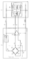
- the electronic control unit 1 supplies a power supply voltage Vcc to the sensor device (here, the pressure sensor 2) through the power supply lines 3 and 4, and the pressure sensor 2 through the signal lines 5 and 6.
- Vcc power supply voltage
- the power supply lines 3 and 4 and the signal lines 5 and 6 are wire harnesses arranged in the vehicle.
- the pressure sensor 2 is assembled on a substrate or modularized.
- the pressure sensor 2 includes piezoresistive elements 7a to 7d formed on the diaphragm so as to form a Wheatstone bridge.
- the bias circuit 8 allows a constant drive current to flow through the Wheatstone bridge terminals 7p and 7q. As a result, a voltage corresponding to the pressure is generated between the terminals 7r and 7s.
- the buffer circuit 9 outputs the sensor signal to the signal lines 5 and 6 in a differential format.
- the electronic control device 1 includes an IC 10.
- the IC 10 includes a differential amplifier 11 that amplifies the sensor signal in the differential signal format, and an A / D converter 12 that A / D converts the amplified sensor signal.
- Each circuit formed in the IC 10 is operated by a power supply voltage Vcc applied via the first power supply line 13 and the second power supply line 14 disposed in the IC.
- the power supply lines 13 and 14 are connected to the power supply lines 3 and 4 described above.
- the differential amplifier 11 includes PNP-type first and second differential input transistors 15 and 16 constituting a differential pair.
- the bases, emitters, and collectors of the transistors 15 and 16 correspond to a control terminal, a first energization terminal, and a second energization terminal, respectively.
- a constant current circuit 17 is provided in common between the power supply line 13 and the emitters of the transistors 15 and 16.
- an active load 20 including NPN transistors 18 and 19 is provided between the collectors of the transistors 15 and 16 and the power supply line 14.
- the emitters of the transistors 18 and 19 are connected to the power supply line 14.
- the collectors of the transistors 18 and 19 are connected to the collectors (nodes Na and Nb) of the transistors 15 and 16, respectively.
- the base and collector of the transistor 18 are connected.
- First and second capacitors 21 and 22 are provided between the collectors of the transistors 15 and 16 and the power supply line 14, respectively.
- Node Nb is an output node of the differential pair.
- the output amplifier circuit 23 outputs a voltage Vo obtained by amplifying the voltage of the node Nb generated in the active load 20.
- the output amplifier circuit 23 includes a constant current circuit 24 connected between the power supply line 13 and the output node Nc, an NPN transistor 25 connected between the output node Nc and the power supply line 14, and between the nodes Nb and Nc.
- the phase compensation capacitor 26 is connected to the.
- the base of the transistor 25 is connected to the node Nb.
- the wire harness composed of the power supply lines 3 and 4 and the signal lines 5 and 6 disposed in the vehicle is provided with noise countermeasures by a shield or the like.
- noise it is difficult to completely block external induced noise.
- a case where AC noise (hereinafter simply referred to as noise) enters the power supply line 4 will be mainly described.
- the frequency of noise that is a problem in the present embodiment is a high frequency (a frequency of 100 MHz or more as an example) at which noise propagates through the parasitic capacitance CBC of the transistors 15 and 16.
- a DC displacement may occur in the output voltage Vo of the differential amplifier. I understood.
- the present inventor conducted circuit analysis and circuit simulation, and elucidated the action of causing DC displacement in the output voltage Vo as follows. That is, in the conventional differential amplifier to which the capacitors 21 and 22 are not added, the impedances in the frequency range of noise between the collectors (nodes Na and Nb) of the transistors 15 and 16 and the power supply line 14 are different from each other. equilibrium). This is because only the active load 20 is connected to the collector of the transistor 15, but the output amplifier circuit 23 is also connected to the collector of the transistor 16 in addition to the active load 20.
- the impedance between the collectors of the transistors 15 and 16 and the power supply line 14 is unbalanced, when noise enters the power supply line 14, a difference occurs in the amplitude of noise applied to the collectors of the transistors 15 and 16.
- the noise propagated to the collectors of the transistors 15 and 16 is applied between the base and the emitter via the parasitic capacitance CBC between the bases and collectors of the transistors 15 and 16. That is, the amplitude difference of the collector potential appears as a difference between the base-emitter voltage VBE.
- the relationship between the base-emitter voltage VBE of the transistor and the collector current Ic is a nonlinear characteristic having an exponential characteristic as shown in FIG.
- sinusoidal noise is applied to the operating point M between the base and the emitter, the increasing range of the collector current Ic from the operating point M becomes larger than the decreasing range of the collector current Ic from the operating point M.
- the DC component (average value) of the collector current of the transistor increases by ⁇ I due to the intrusion of noise.
- the DC displacement of the output voltage Vo can be reduced if the impedances between the collectors of the transistors 15 and 16 and the power supply line 14 are balanced in the noise frequency range and balanced. I understand that I can do it. Therefore, in the differential amplifier 11, both impedances are balanced by providing capacitors 21 and 22 between the nodes Na and Nb and the power supply line 14, respectively.
- the equilibrium condition is expressed by equation (1).
- the left side is the impedance between the collector of the transistor 15 and the power supply line 14.
- the right side is the impedance between the collector of the transistor 16 and the power supply line 14.
- the capacitance values Cp and Cm are described below so that the impedance between each collector of the transistors 15 and 16 and the power supply line 14 has a balance (predetermined balance) at which a DC displacement suppression effect can be obtained. It is determined by any one of the first to third methods.
- the capacitance values Cp and Cm are theoretically derived from the limit value of the direct current displacement of the output voltage Vo.
- the values of ⁇ Vo ′ and ⁇ Io can be derived from circuit characteristics.
- Vbias represents the base-emitter voltage of the transistor 16 when no noise has entered
- Vn represents the amplitude of the noise.
- hfe is a current amplification factor
- Is is a saturation current
- q is an electron charge
- k is a Boltzmann constant
- T is an absolute temperature.
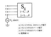
- S41, S42, and S43 are S parameters representing propagation characteristics from the power supply line 14 to the emitter terminals and base terminals of the transistors 15 and 16, as shown in FIG.
- the capacitance values Cp and Cm may be determined so as to satisfy the expression (3).
- the collector current ic2 of the transistor 16 can be expressed by equation (5).
- equation (6) is obtained by integrating equation (5).
- a bias voltage Vbias and a noise voltage Vnoise1 expressed by equation (7) are applied between the base and emitter of the transistor 15.
- v1 is the amplitude of noise.
- the collector current ic1 of the transistor 15 can be expressed by equation (8).
- Equation (9) is obtained by integrating Equation (8).
- reference numeral 1 denotes the emitter terminals of the transistors 15 and 16
- reference numeral 2 denotes the base terminal of the transistor
- reference numeral 3 denotes the base terminal of the transistor 16
- reference numeral 4 denotes the power supply line 14.
- the noise voltage is defined by equation (11).
- the voltage amplitude between the base and emitter of the transistor 15 can be expressed by equation (12).
- Equation (2) Substituting Equations (13) and (14) into Equation (10) yields Equation (2).
- the impedances between the collectors of the transistors 15 and 16 and the power supply line 14 are dominated by the impedances 1 / (j ⁇ Cp) and 1 / (j ⁇ Cm) of the capacitors 21 and 22.
- the capacitance values Cp and Cm are made equal, the impedance balance between the collectors of the transistors 15 and 16 and the power supply line 14 can be improved, and the DC displacement of the output voltage Vo can be suppressed.
- the capacitance values Cp and Cm are determined so as to obtain a predetermined balance. For example, when the noise frequency is 100 MHz or more, the parasitic capacitances of the transistors 15 and 16 are about several tens of fF, so the capacitance values Cp and Cm may be set to about several tens of pF.
- the differential amplifier 11 of this embodiment includes the capacitors 21 and 22 between the collectors of the transistors 15 and 16 and the power supply line 14.
- the impedance between the collectors of the transistors 15 and 16 and the power supply line 14 can be made close to each other and balanced. As a result, it is possible to reduce the DC displacement that appears in the output voltage Vo.
- noise that has entered from the output terminal of the differential amplifier 11 is bypassed to the power supply line 14 via the capacitor 22, noise added between the base and emitter of the transistor 25 of the output amplifier circuit 23 is reduced. Thereby, even when noise enters from the output terminal, the direct current displacement due to the nonlinearity of the transistor 25 can be suppressed, and the immunity resistance against the noise can be maintained high.
- the impedance between the collectors of the transistors 15 and 16 and the power supply line 14 may be balanced.
- the capacitance values of the capacitors 21 and 22 are preferably set so that the impedance between the collector of the transistor 15 and the power supply line 14 and the impedance between the collector of the transistor 16 and the power supply line 14 are equal to each other. .
- the capacitance values Cp and Cm of the capacitors 21 and 22 are determined so that the phase margin is secured to a predetermined value or more necessary for stable operation.
- a configuration using a FET such as a MOS transistor instead of the bipolar transistor may be used.
- the configurations of the constant current circuit 17, the active load 20, and the output amplifier circuit 23 are not limited to the illustrated configurations, and can be variously changed as long as the same operation is achieved.
- the first and second differential input transistors are composed of NPN transistors (N-channel type if FET), the constant current circuit 17 is disposed on the power supply line 14 side, and the active load 20 is disposed on the power supply line 13 side. It is good also as a structure. In this case, direct current displacement due to noise entering the power supply line 13 can be prevented.
Landscapes
- Engineering & Computer Science (AREA)
- Power Engineering (AREA)
- Amplifiers (AREA)
Abstract
L'invention concerne un amplificateur différentiel comprenant des condensateurs (21, 22) entre une ligne d'alimentation électrique (14) et les collecteurs de transistors (15, 16), amenant les impédances entre ladite ligne d'alimentation électrique (14) et les collecteurs des transistors (15, 16) respectifs à des valeurs d'équilibre proches les unes des autres. Cela est réalisé de telle sorte que si du bruit pénètre dans la ligne d'alimentation électrique (14), les amplitudes du bruit appliquées aux collecteurs des transistors (15, 16) respectifs sont approximativement égales, tout comme le sont les tensions base-émetteur dues à la capacité parasite. Le résultat est que le courant de décalage CC qui circule en raison de la caractéristique non linéaire des transistors (15, 16) est annulé, ce qui minimise le décalage CC dans la tension de sortie (Vo).
Applications Claiming Priority (2)
| Application Number | Priority Date | Filing Date | Title |
|---|---|---|---|
| JP2013126584A JP2015002457A (ja) | 2013-06-17 | 2013-06-17 | 差動増幅器 |
| JP2013-126584 | 2013-06-17 |
Publications (1)
| Publication Number | Publication Date |
|---|---|
| WO2014203473A1 true WO2014203473A1 (fr) | 2014-12-24 |
Family
ID=52104225
Family Applications (1)
| Application Number | Title | Priority Date | Filing Date |
|---|---|---|---|
| PCT/JP2014/002919 Ceased WO2014203473A1 (fr) | 2013-06-17 | 2014-06-03 | Amplificateur différentiel |
Country Status (2)
| Country | Link |
|---|---|
| JP (1) | JP2015002457A (fr) |
| WO (1) | WO2014203473A1 (fr) |
Citations (8)
| Publication number | Priority date | Publication date | Assignee | Title |
|---|---|---|---|---|
| JPH06260855A (ja) * | 1993-03-08 | 1994-09-16 | Nec Ic Microcomput Syst Ltd | 多段直結増幅回路 |
| JPH08204468A (ja) * | 1995-01-20 | 1996-08-09 | Seikosha Co Ltd | 演算増幅器 |
| JPH08274259A (ja) * | 1995-03-29 | 1996-10-18 | Nissan Motor Co Ltd | 演算増幅器回路 |
| JP2000049546A (ja) * | 1998-07-28 | 2000-02-18 | Mitsubishi Electric Corp | オフセット調整装置 |
| WO2002052737A1 (fr) * | 2000-12-22 | 2002-07-04 | Niigata Seimitsu Co., Ltd. | Circuit de limitation |
| JP2008306562A (ja) * | 2007-06-08 | 2008-12-18 | Asahi Kasei Electronics Co Ltd | 演算増幅器 |
| JP2009171350A (ja) * | 2008-01-17 | 2009-07-30 | Nsc Co Ltd | ラジオ受信機およびこれに用いる受信用半導体集積回路 |
| JP2012204860A (ja) * | 2011-03-23 | 2012-10-22 | Toshiba Corp | 半導体集積回路および受信装置 |
-
2013
- 2013-06-17 JP JP2013126584A patent/JP2015002457A/ja active Pending
-
2014
- 2014-06-03 WO PCT/JP2014/002919 patent/WO2014203473A1/fr not_active Ceased
Patent Citations (8)
| Publication number | Priority date | Publication date | Assignee | Title |
|---|---|---|---|---|
| JPH06260855A (ja) * | 1993-03-08 | 1994-09-16 | Nec Ic Microcomput Syst Ltd | 多段直結増幅回路 |
| JPH08204468A (ja) * | 1995-01-20 | 1996-08-09 | Seikosha Co Ltd | 演算増幅器 |
| JPH08274259A (ja) * | 1995-03-29 | 1996-10-18 | Nissan Motor Co Ltd | 演算増幅器回路 |
| JP2000049546A (ja) * | 1998-07-28 | 2000-02-18 | Mitsubishi Electric Corp | オフセット調整装置 |
| WO2002052737A1 (fr) * | 2000-12-22 | 2002-07-04 | Niigata Seimitsu Co., Ltd. | Circuit de limitation |
| JP2008306562A (ja) * | 2007-06-08 | 2008-12-18 | Asahi Kasei Electronics Co Ltd | 演算増幅器 |
| JP2009171350A (ja) * | 2008-01-17 | 2009-07-30 | Nsc Co Ltd | ラジオ受信機およびこれに用いる受信用半導体集積回路 |
| JP2012204860A (ja) * | 2011-03-23 | 2012-10-22 | Toshiba Corp | 半導体集積回路および受信装置 |
Also Published As
| Publication number | Publication date |
|---|---|
| JP2015002457A (ja) | 2015-01-05 |
Similar Documents
| Publication | Publication Date | Title |
|---|---|---|
| JP2001223546A (ja) | 多段信号増幅回路 | |
| CN105556834A (zh) | 放大电路 | |
| KR101834255B1 (ko) | 영상신호 출력 회로 | |
| JP4573602B2 (ja) | 増幅装置 | |
| US8624671B2 (en) | Audio amplifying circuit with improved noise performance | |
| US11199564B2 (en) | Current sensing circuit | |
| US11101776B2 (en) | Common source preamplifier for a MEMS capacitive sensor | |
| US6734720B2 (en) | Operational amplifier in which the idle current of its output push-pull transistors is substantially zero | |
| US8803493B2 (en) | Voltage regulator with differentiating and amplifier circuitry | |
| WO2014203473A1 (fr) | Amplificateur différentiel | |
| JP2000022451A (ja) | 信号処理回路装置 | |
| JP2006319388A (ja) | 自動利得制御回路及びそれを用いた正弦波発振回路 | |
| JP5388670B2 (ja) | センサ信号処理回路 | |
| JP4360267B2 (ja) | 増幅回路 | |
| RU2292636C1 (ru) | Дифференциальный усилитель с повышенным ослаблением синфазного сигнала | |
| JP2006033091A (ja) | センサユニット及びセンサ信号処理回路 | |
| JP6933797B2 (ja) | オーディオアンプおよびオーディオパワーアンプ | |
| JP2021010048A (ja) | 演算増幅器 | |
| US10461706B1 (en) | Differential amplifier including cancellation capacitors | |
| JP5060890B2 (ja) | 半導体装置 | |
| Litovski | 4 Discrete and Integrated Power Amplifier Circuits | |
| JP2016086230A (ja) | センサ装置 | |
| TWI508434B (zh) | 放大器電路及放大訊號方法 | |
| US9093992B1 (en) | Current-boosting output stage with short-circuit protection | |
| JP5350882B2 (ja) | 容量増倍回路 |
Legal Events
| Date | Code | Title | Description |
|---|---|---|---|
| 121 | Ep: the epo has been informed by wipo that ep was designated in this application |
Ref document number: 14812934 Country of ref document: EP Kind code of ref document: A1 |
|
| NENP | Non-entry into the national phase |
Ref country code: DE |
|
| 122 | Ep: pct application non-entry in european phase |
Ref document number: 14812934 Country of ref document: EP Kind code of ref document: A1 |