WO2014203552A1 - 電力変換装置 - Google Patents
電力変換装置 Download PDFInfo
- Publication number
- WO2014203552A1 WO2014203552A1 PCT/JP2014/051886 JP2014051886W WO2014203552A1 WO 2014203552 A1 WO2014203552 A1 WO 2014203552A1 JP 2014051886 W JP2014051886 W JP 2014051886W WO 2014203552 A1 WO2014203552 A1 WO 2014203552A1
- Authority
- WO
- WIPO (PCT)
- Prior art keywords
- power
- case
- power semiconductor
- conversion device
- opening
- Prior art date
- Legal status (The legal status is an assumption and is not a legal conclusion. Google has not performed a legal analysis and makes no representation as to the accuracy of the status listed.)
- Ceased
Links
Images






Classifications
-
- H—ELECTRICITY
- H02—GENERATION; CONVERSION OR DISTRIBUTION OF ELECTRIC POWER
- H02M—APPARATUS FOR CONVERSION BETWEEN AC AND AC, BETWEEN AC AND DC, OR BETWEEN DC AND DC, AND FOR USE WITH MAINS OR SIMILAR POWER SUPPLY SYSTEMS; CONVERSION OF DC OR AC INPUT POWER INTO SURGE OUTPUT POWER; CONTROL OR REGULATION THEREOF
- H02M7/00—Conversion of AC power input into DC power output; Conversion of DC power input into AC power output
- H02M7/003—Constructional details, e.g. physical layout, assembly, wiring or busbar connections
-
- H—ELECTRICITY
- H05—ELECTRIC TECHNIQUES NOT OTHERWISE PROVIDED FOR
- H05K—PRINTED CIRCUITS; CASINGS OR CONSTRUCTIONAL DETAILS OF ELECTRIC APPARATUS; MANUFACTURE OF ASSEMBLAGES OF ELECTRICAL COMPONENTS
- H05K7/00—Constructional details common to different types of electric apparatus
- H05K7/14—Mounting supporting structure in casing or on frame or rack
- H05K7/1422—Printed circuit boards receptacles, e.g. stacked structures, electronic circuit modules or box like frames
- H05K7/1427—Housings
- H05K7/1432—Housings specially adapted for power drive units or power converters
- H05K7/14322—Housings specially adapted for power drive units or power converters wherein the control and power circuits of a power converter are arranged within the same casing
-
- H—ELECTRICITY
- H05—ELECTRIC TECHNIQUES NOT OTHERWISE PROVIDED FOR
- H05K—PRINTED CIRCUITS; CASINGS OR CONSTRUCTIONAL DETAILS OF ELECTRIC APPARATUS; MANUFACTURE OF ASSEMBLAGES OF ELECTRICAL COMPONENTS
- H05K7/00—Constructional details common to different types of electric apparatus
- H05K7/20—Modifications to facilitate cooling, ventilating, or heating
- H05K7/2089—Modifications to facilitate cooling, ventilating, or heating for power electronics, e.g. for inverters for controlling motor
- H05K7/209—Heat transfer by conduction from internal heat source to heat radiating structure
-
- H—ELECTRICITY
- H02—GENERATION; CONVERSION OR DISTRIBUTION OF ELECTRIC POWER
- H02M—APPARATUS FOR CONVERSION BETWEEN AC AND AC, BETWEEN AC AND DC, OR BETWEEN DC AND DC, AND FOR USE WITH MAINS OR SIMILAR POWER SUPPLY SYSTEMS; CONVERSION OF DC OR AC INPUT POWER INTO SURGE OUTPUT POWER; CONTROL OR REGULATION THEREOF
- H02M1/00—Details of apparatus for conversion
- H02M1/32—Means for protecting converters other than automatic disconnection
- H02M1/327—Means for protecting converters other than automatic disconnection against abnormal temperatures
Definitions
- the present invention relates to a power conversion device.
- Inverters which are power conversion devices, are widely used as speed control devices for AC motors in industry and home appliances.
- IPM integer power modules
- Patent Document 1 “as a result of placing the lid portion 20c on the substrate 50, the plurality of lead frames 23 and the plurality of metal foils 12 on the substrate 50 come into contact with each other. The parts are soldered to electrically connect each lead frame 23 and each metal foil 12. Also, the lead frame 23 and each metal foil 12 are joined, so that the lid 20c. Is fixed on the substrate 50 ".
- FIG. 20 discloses an opening that penetrates the lead frame (lead terminal), an empty opening that does not penetrate the lead frame, and an opening for gel injection.
- Line 20 says, “Compared to the conventional M711 package with the same rated current, the compact flexible PIM has reduced the mounting area by 45% and the mass by 75% ⁇ ⁇ . This reduces the size and cost of customer equipment. It can make a big contribution. ”
- Patent Document 1 and Non-Patent Document 1 describe an opening that penetrates the lead frame (lead terminal) and an empty opening that does not penetrate the lead frame on the upper surface of the power semiconductor module.
- the degree of freedom in manufacturing the power semiconductor module can be increased.
- the lead frame can be provided at any location
- the surrounding air is supplied to the inside of the module through the empty opening through which the lead frame does not penetrate and the opening for gel injection, when the power semiconductor breaks down, it easily combines with the surrounding air and ignites. easy.
- the conventional power semiconductor module is composed of a hard resin and a lid, when the power semiconductor breaks down, it has a structure that is not easily combined with the surrounding air.
- a power semiconductor a cooling fin that cools the power semiconductor, a first case that is disposed between the power semiconductor and the cooling fin and includes an opening that matches the shape of the power semiconductor, and the power semiconductor. And a second case for covering the lead terminal opening.
- a flame due to abnormal heat generated inside is ejected from an empty opening or a gel injection opening that does not penetrate the lead frame, and the other inside the power converter. Secondary fire spread due to the spread of fire to parts and the like can be prevented.
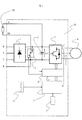
- Example 1 is an example of a configuration diagram of a power converter according to the present invention.
- FIG. 1 shows a case where an AC power source is used as an arbitrary input power source.
- Forward converter unit 1 converts AC power into DC power.
- the smoothing capacitor 2 is provided on the output side of the forward converter unit 1.
- the reverse converter unit 3 converts DC power into AC power having an arbitrary frequency.
- an IGBT is mounted in the inverse converter unit 3 as a typical switching element.
- the switching element is not limited to the IGBT, and any element having a form as a switching element may be used.
- the cooling fan 6 cools the power semiconductor modules in the forward converter unit 1, the regenerative braking unit 9, and the reverse converter unit 3.
- the digital operation panel 7 sets, changes, abnormal states, and monitor displays various control data of the power conversion device.
- the operation panel 7 is provided with a display unit capable of displaying an abnormality. When an abnormality is detected in the power conversion device, the display is displayed on the display unit.
- the type of the operation panel 7 of the present embodiment is not particularly limited. However, the operation panel 7 is configured as a digital operation panel so that the operation can be performed while viewing the display on the display unit in consideration of the operability of the apparatus user. .
- the display unit is not necessarily configured integrally with the operation panel 7, but it is desirable that the display unit be configured integrally so that an operator of the operation panel 7 can operate while viewing the display.
- Various control data of the power converter input from the operation panel 7 is stored in a storage unit (not shown).
- the control circuit 5 controls the switching elements in the reverse converter unit 3 and the regenerative braking unit 9 based on various control data input from the digital operation panel 7, and also has a function of controlling the power converter 10 as a whole. Therefore, a microcomputer (control arithmetic unit) is mounted and is configured to perform necessary control processing according to various control data input from the digital operation panel 7.
- a microcomputer control arithmetic unit that performs an operation based on information from storage data of a storage unit that stores various control data is mounted.
- the current detector CT detects the U-phase and W-phase line currents of the AC motor.
- FIG. 1 shows an example in which two CTs are used, but three CTs may be used to detect line currents of each U phase, V phase, and W phase.
- the drive circuit 8 drives the switching elements in the inverse converter unit 3 and the regenerative braking unit 9 based on a command from the control circuit 5.
- a switching regulator circuit (DC / DC converter) is mounted in the drive circuit 8, and each DC voltage necessary for the operation of the power converter is generated and supplied to each component.
- the regenerative braking resistor BR plays a role of consuming rotational energy during deceleration of the AC motor as heat energy to the resistor.
- the DC power supply + side is connected to the DC terminal P side, and the DC power supply -side is connected to the DC terminal N side.
- the AC terminals R, S, and T may be connected, the DC power supply + side may be connected to this connection point, and the DC power supply N side may be connected to the DC power supply negative side.
- the positive side of the DC power source may be connected to the P side, the AC terminals R, S, and T may be connected, and the negative side of the DC power source may be connected to this connection point.
- FIG. 2 is an example of a bird's-eye view of the power conversion device according to the present invention.
- Example 2 of the power converter device by this invention is demonstrated using a figure below.
- the power semiconductor PM is a module including a forward converter unit 1, an inverse converter unit 3, and a regenerative braking unit 9. A state where a case 15 is attached to the power semiconductor is shown.
- the power semiconductor PM is fixed to the cooling fin by screws (not shown).
- a lead terminal of the power semiconductor is passed through a through hole provided in the substrate PCB on which the drive circuit 8 is mounted, and is electrically connected by solder (solder).
- the substrate on which the control circuit 5 is mounted and the substrate PCB on which the drive circuit 8 is mounted are connected by an electric wire.
- the cooling fin 11 conducts heat from the power semiconductor, which is a heating element, sends air to the cooling fin by a cooling fan (not shown), and performs heat exchange to dissipate heat by an air cooling method.
- the positioning case 16 is provided with an opening in advance according to the power semiconductor so that the mounting position of the power semiconductor can be easily determined when the power semiconductor PM is mounted on the cooling fin, and the mounting position of the power semiconductor is fixed.
- the module composed of the forward converter unit 1, the reverse converter unit 3, and the regenerative braking unit 9 is taken as an example.
- the power semiconductor and the reverse converter unit 3 composed of only the forward converter unit 1 are used. Even if two power semiconductors composed of the regenerative braking unit 9 are used, the forward converter unit 1, the reverse converter unit 3, and the regenerative braking unit 9 are used individually for the three power semiconductors.
- the intention of the invention remains the same.
- the casing of the power conversion device includes a cooling fin 11, a casing 12, a wire drawing plate 13, and a surface cover 14.
- FIG. 3 is a bird's-eye view (first form) of the positioning case 16 of the power conversion device according to the present invention.
- (A) is a bird's eye view in which protrusions (barriers) 17 are provided on the four sides of the opening A provided in the positioning case 16 according to the power semiconductor PM.
- (B) is a bird's-eye view in which protrusions (barriers) 17 are provided on two sides of the opening A provided in the positioning case 16.
- (C) is a bird's eye view in which no protrusion (barrier) is provided in the opening A provided in the positioning case 16.
- the height h1 of the protrusion 17 is designed to be lower than the height h2 (see FIG. 4A) of the power semiconductor PM.
- the projections 17 are provided on the four sides and two sides of the opening A, but not provided, but the number of sides on which the projections are provided is not limited.
- (D) is a front view and a bird's-eye view of a state in which the power semiconductor covered with the positioning case 16 and the case 15 described in (c) is mounted on a cooling fin.
- (E) is a front view and a bird's-eye view of a state in which the power semiconductor covered with the positioning case and the case 15 described in (a) is mounted on a cooling fin.
- the projections 17 on the four sides provided in the positioning case 16 hold the case 15 covered with the power semiconductor PM, and the power is prevented so that flames due to abnormal heat generation are not ejected due to an increase in internal pressure inside the module when the power semiconductor is broken. It can be seen that the gap with the semiconductor can be reduced.
- the gaps on the four sides can be made smaller than in the case (c) in which no protrusions are provided on the opening A. The effect of suppressing the force that comes out is great.
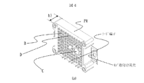
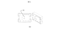
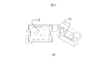
- FIG. 4 is a bird's-eye view (second embodiment) of the case 15 of the power conversion device according to the present invention.
- Example 2 of the power converter device by this invention is demonstrated using a figure below.
- (A) is an example of a bird's-eye view of the power semiconductor PM, and has 69 empty openings B and one opening C for gel injection through which lead terminals do not penetrate. Of course, there is also a gap on the contact surface D through which the 20 lead terminals pass.
- the reason for providing a plurality of openings is that when manufacturing custom power semiconductor modules dedicated to customers, if a plurality of openings are provided in advance, the lead frame can be provided at any place, and the custom power semiconductor This is because the module has a manufacturing advantage that a standard power semiconductor module case can be shared.
- (B) is a front view and a bird's-eye view of the case 15 in one embodiment.
- the cover is provided with oval and circular openings in accordance with all the lead terminal positions of the power semiconductor. Of course, it may be a rectangular opening.
- (C) is a front view and a bird's-eye view of the case 15 in another embodiment.
- the difference from the cover described in the embodiment of (b) is to secure an electrical insulation distance from the component mounted on the back surface of the substrate PCB, the lead of the component, and the screw for mounting the power semiconductor to the cooling fin.
- the protrusion part E provided in both ends. Details of this example will be described later.
- (D) is a front view and a rear bird's-eye view of the case 15 provided with a protrusion (boss) 18 that closes the opening C for gel injection of the power semiconductor.
- the bird's-eye view shows a state in which the case 15 is viewed from the back so that the protrusion 18 can be identified.
- the protrusion is slightly tapered so that it can be easily inserted into the opening for gel injection, and the tip is thin. Of course, it may be a quadrangular protrusion (boss).
- the length of the protrusion may be designed according to the depth of the power semiconductor gel injection opening.
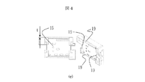
- (E) is a front view and a bird's-eye view of a case in which protrusions 19 are provided on four sides.
- the protrusions 19 provided on the four sides of the case have contact with the protrusions provided on the four sides on the back surface of the substrate PCB on which the drive circuit 8 is mounted, so that the back surface of the substrate PCB serves as a lid and can eliminate gaps. It is what I did.
- the protrusion 19 is not limited to four sides, and two sides are also effective.
- the method (e) can eliminate the gap more effectively. Details of this example will be described later.
- (F) is a front view and a bird's-eye view of a case in which 20 circular openings F are provided in accordance with the shape and number of lead terminals of the power semiconductor.
- the gap between the lead terminal and the opening of the case can be further reduced with respect to the case of the embodiment in (b) to (e).
- (G) is a bird's-eye view showing a state where the case is attached to the power semiconductor.
- the purpose is to cover the power semiconductor with the case by moving the case in the direction of the arrow and covering the power semiconductor so that the 20 lead terminals of the power semiconductor pass through the opening provided in the case 15.
- This is a feature of the present invention.
- the case thickness t is designed to be 0.71 mm or more.
- the case covers the power semiconductor, and a flame due to abnormal heat generated inside when the semiconductor module is broken is ejected from an empty opening B or an opening C for gel injection that does not penetrate the lead frame. Prevent secondary fire spreading due to fire spreading to other parts inside.
- the case is molded using an insulating resin such as silicon or plastic. Considering ease of handling, the case made of highly flexible silicon is more realistic in terms of workability.
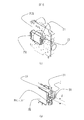
- FIG. 5 is a bird's-eye view (third embodiment) showing the relationship between the substrate PCB and the case 15 of the power conversion device according to the present invention.
- (A) is a bird's-eye view showing a state in which a lead terminal of a power semiconductor is passed through a through hole (not shown) of a substrate PCB on which the drive circuit 8 is mounted and is electrically connected with solder.
- the bird's-eye view is a view seen from the back side of the substrate.
- ⁇ Lead feet of the mounted parts pass through through holes (not shown) on the board and come out from the back side of the board. 20 and 21 are shown as typical lead feet on the back surface.
- the power semiconductor with the case 15 covered on the cooling fin and the positioning case 16 are attached, and the lead terminal of the power semiconductor is inserted into the through hole of the board and soldered. For this reason, when the projections 19 provided on the four sides of the case 15 shown in FIG. 4 (e) are in contact with the back surface of the substrate, the back surface of the substrate PCB serves as a lid, and a gap can be eliminated.
- the component mounting design of the substrate may be made in advance by avoiding the protrusion so that the component is not mounted on the portion where the rear surface of the substrate contacts the protrusion.
- (B) is an enlarged view of a portion surrounded by a dotted line in (a).
- the power semiconductor is attached to a cooling fin (not shown) with a mounting screw.
- a mounting screw This is an example in which the distance d between the head of the screw and the lead foot 20 of the mounting component coming out from the back surface of the board is not equal to or more than a predetermined insulation distance. Electricity provided on the cover 15 covered with the power semiconductor Since the lead foot is surrounded by the protruding portion E for securing the effective insulation distance, the insulation distance can be reduced and the power converter can be downsized.
- FIG. 6 is a diagram (fourth embodiment) in a state where an insulating resin is applied to the opening of the power semiconductor of the power conversion device according to the present invention.
- Embodiments of a power converter according to Embodiment 4 of the present invention will be described below with reference to the drawings.
- Example 1 The difference from Example 1 is that silicon or an insulating resin is applied instead of the molded case 15 to close the opening B or the opening C for gel injection.
- a place where an insulating resin is collectively applied to a part of an opening of a power semiconductor and a place where potting is applied are described as examples. Either one of these methods (batch application or potting application) may be used to apply all the openings (B and C) with an insulating resin, or both (batch application and potting application) may be used together in consideration of workability. It is more realistic to apply all the openings (B and C). Of course, silicon or insulating resin may be applied around the opening D through which the lead frame passes.
- (B) shows an enlarged bird's-eye view of the power semiconductor describing the relationship between the opening and the lead terminal.
- the flame due to abnormal heat generated inside when the semiconductor module is broken is blown out from an empty opening or a gel injection opening that does not penetrate the lead frame. Secondary fire spreading of the power conversion device due to fire spreading to other components inside the power conversion device can be prevented.
Landscapes
- Engineering & Computer Science (AREA)
- Microelectronics & Electronic Packaging (AREA)
- Power Engineering (AREA)
- Physics & Mathematics (AREA)
- Thermal Sciences (AREA)
- Inverter Devices (AREA)
Priority Applications (2)
| Application Number | Priority Date | Filing Date | Title |
|---|---|---|---|
| EP14813134.5A EP3012958B1 (de) | 2013-06-19 | 2014-01-29 | Stromwandlungsvorrichtung |
| CN201480034841.2A CN105308847B (zh) | 2013-06-19 | 2014-01-29 | 电力转换装置 |
Applications Claiming Priority (2)
| Application Number | Priority Date | Filing Date | Title |
|---|---|---|---|
| JP2013128080A JP6082664B2 (ja) | 2013-06-19 | 2013-06-19 | 電力変換装置 |
| JP2013-128080 | 2013-06-19 |
Publications (1)
| Publication Number | Publication Date |
|---|---|
| WO2014203552A1 true WO2014203552A1 (ja) | 2014-12-24 |
Family
ID=52104301
Family Applications (1)
| Application Number | Title | Priority Date | Filing Date |
|---|---|---|---|
| PCT/JP2014/051886 Ceased WO2014203552A1 (ja) | 2013-06-19 | 2014-01-29 | 電力変換装置 |
Country Status (4)
| Country | Link |
|---|---|
| EP (1) | EP3012958B1 (de) |
| JP (1) | JP6082664B2 (de) |
| CN (1) | CN105308847B (de) |
| WO (1) | WO2014203552A1 (de) |
Cited By (1)
| Publication number | Priority date | Publication date | Assignee | Title |
|---|---|---|---|---|
| CN113396479A (zh) * | 2019-02-14 | 2021-09-14 | 株式会社日立产机系统 | 电力转换装置 |
Families Citing this family (3)
| Publication number | Priority date | Publication date | Assignee | Title |
|---|---|---|---|---|
| CN106505875B (zh) * | 2016-11-14 | 2019-05-28 | 广州瓦良格机器人科技有限公司 | 一种防腐防爆智能ipm变频模块 |
| JP7154907B2 (ja) | 2018-09-14 | 2022-10-18 | 株式会社東芝 | 半導体モジュール |
| CN119252152B (zh) * | 2024-04-18 | 2025-08-26 | 荣耀终端股份有限公司 | 一种电子设备及电子设备的组装方法 |
Citations (3)
| Publication number | Priority date | Publication date | Assignee | Title |
|---|---|---|---|---|
| JPH0636824A (ja) * | 1992-07-15 | 1994-02-10 | Matsushita Electric Ind Co Ltd | 防水・防塵コネクタ |
| JP2008288414A (ja) | 2007-05-18 | 2008-11-27 | Fuji Electric Device Technology Co Ltd | 半導体モジュール及び半導体モジュールの製造方法 |
| JP2012191849A (ja) * | 2007-04-20 | 2012-10-04 | Hitachi Industrial Equipment Systems Co Ltd | 電力変換装置及びパワーサイクル寿命予測方法 |
Family Cites Families (3)
| Publication number | Priority date | Publication date | Assignee | Title |
|---|---|---|---|---|
| FR2724283B1 (fr) * | 1994-09-02 | 1996-10-18 | Schneider Electric Sa | Variateur electronique de vitesse |
| US6147869A (en) * | 1997-11-24 | 2000-11-14 | International Rectifier Corp. | Adaptable planar module |
| WO2008087875A1 (ja) * | 2007-01-18 | 2008-07-24 | Kabushiki Kaisha Yaskawa Denki | モータ制御装置 |
-
2013
- 2013-06-19 JP JP2013128080A patent/JP6082664B2/ja active Active
-
2014
- 2014-01-29 CN CN201480034841.2A patent/CN105308847B/zh active Active
- 2014-01-29 EP EP14813134.5A patent/EP3012958B1/de active Active
- 2014-01-29 WO PCT/JP2014/051886 patent/WO2014203552A1/ja not_active Ceased
Patent Citations (3)
| Publication number | Priority date | Publication date | Assignee | Title |
|---|---|---|---|---|
| JPH0636824A (ja) * | 1992-07-15 | 1994-02-10 | Matsushita Electric Ind Co Ltd | 防水・防塵コネクタ |
| JP2012191849A (ja) * | 2007-04-20 | 2012-10-04 | Hitachi Industrial Equipment Systems Co Ltd | 電力変換装置及びパワーサイクル寿命予測方法 |
| JP2008288414A (ja) | 2007-05-18 | 2008-11-27 | Fuji Electric Device Technology Co Ltd | 半導体モジュール及び半導体モジュールの製造方法 |
Non-Patent Citations (2)
| Title |
|---|
| FUJI ELECTRIC REVIEW, vol. 85, no. 6, 2012, pages 426 - 429 |
| See also references of EP3012958A4 |
Cited By (2)
| Publication number | Priority date | Publication date | Assignee | Title |
|---|---|---|---|---|
| CN113396479A (zh) * | 2019-02-14 | 2021-09-14 | 株式会社日立产机系统 | 电力转换装置 |
| CN113396479B (zh) * | 2019-02-14 | 2023-09-22 | 株式会社日立产机系统 | 电力转换装置 |
Also Published As
| Publication number | Publication date |
|---|---|
| CN105308847A (zh) | 2016-02-03 |
| EP3012958A1 (de) | 2016-04-27 |
| EP3012958B1 (de) | 2020-04-01 |
| EP3012958A4 (de) | 2017-02-15 |
| JP6082664B2 (ja) | 2017-02-15 |
| JP2015006015A (ja) | 2015-01-08 |
| CN105308847B (zh) | 2018-04-13 |
Similar Documents
| Publication | Publication Date | Title |
|---|---|---|
| US7848104B2 (en) | Power module | |
| CN104742960B (zh) | 电子控制单元和具有电子控制单元的电动助力转向装置 | |
| JP5586866B2 (ja) | 電力変換装置 | |
| CN100428617C (zh) | 半导体元件的温度检测方法和电力变换装置 | |
| JP5974988B2 (ja) | 電子装置 | |
| JP2017017975A (ja) | 電動コンプレッサ | |
| JP6082664B2 (ja) | 電力変換装置 | |
| JP6647152B2 (ja) | Dcブラシレスモータおよび換気送風機 | |
| JP6020379B2 (ja) | 半導体装置 | |
| JP2015099846A (ja) | 半導体装置および半導体装置の製造方法 | |
| JPWO2014064822A1 (ja) | パワー半導体モジュールおよびこれを搭載した電力変換装置 | |
| JP4034766B2 (ja) | 回路基板及び電動送風機 | |
| JP3651406B2 (ja) | 電力変換装置 | |
| JP5349817B2 (ja) | 保護回路、半導体装置、電気機器 | |
| JP2002238260A (ja) | 半導体装置 | |
| JP3566505B2 (ja) | インバータ装置 | |
| WO2016113858A1 (ja) | モータ及びモータの製造方法 | |
| CN114121927A (zh) | 半导体电路及其应用装置 | |
| WO2017002693A1 (ja) | 電動コンプレッサ | |
| JP2022116613A (ja) | 電力変換装置 | |
| JP6439834B2 (ja) | 制御装置 | |
| JP2014049610A (ja) | 回路基板 | |
| JP5802798B2 (ja) | 電力変換装置 | |
| JP4930406B2 (ja) | パワー半導体装置及びこれを用いたインバータ装置 | |
| JP2024166117A (ja) | コンデンサ、電力変換装置およびモータユニット |
Legal Events
| Date | Code | Title | Description |
|---|---|---|---|
| WWE | Wipo information: entry into national phase |
Ref document number: 201480034841.2 Country of ref document: CN |
|
| 121 | Ep: the epo has been informed by wipo that ep was designated in this application |
Ref document number: 14813134 Country of ref document: EP Kind code of ref document: A1 |
|
| WWE | Wipo information: entry into national phase |
Ref document number: 2014813134 Country of ref document: EP |
|
| NENP | Non-entry into the national phase |
Ref country code: DE |