WO2014203565A1 - Dispositif d'affichage à cristaux liquides et son procédé de fabrication - Google Patents
Dispositif d'affichage à cristaux liquides et son procédé de fabrication Download PDFInfo
- Publication number
- WO2014203565A1 WO2014203565A1 PCT/JP2014/054961 JP2014054961W WO2014203565A1 WO 2014203565 A1 WO2014203565 A1 WO 2014203565A1 JP 2014054961 W JP2014054961 W JP 2014054961W WO 2014203565 A1 WO2014203565 A1 WO 2014203565A1
- Authority
- WO
- WIPO (PCT)
- Prior art keywords
- liquid crystal
- pretilt
- photo
- region
- alignment film
- Prior art date
- Legal status (The legal status is an assumption and is not a legal conclusion. Google has not performed a legal analysis and makes no representation as to the accuracy of the status listed.)
- Ceased
Links
Images


Classifications
-
- G—PHYSICS
- G02—OPTICS
- G02F—OPTICAL DEVICES OR ARRANGEMENTS FOR THE CONTROL OF LIGHT BY MODIFICATION OF THE OPTICAL PROPERTIES OF THE MEDIA OF THE ELEMENTS INVOLVED THEREIN; NON-LINEAR OPTICS; FREQUENCY-CHANGING OF LIGHT; OPTICAL LOGIC ELEMENTS; OPTICAL ANALOGUE/DIGITAL CONVERTERS
- G02F1/00—Devices or arrangements for the control of the intensity, colour, phase, polarisation or direction of light arriving from an independent light source, e.g. switching, gating or modulating; Non-linear optics
- G02F1/01—Devices or arrangements for the control of the intensity, colour, phase, polarisation or direction of light arriving from an independent light source, e.g. switching, gating or modulating; Non-linear optics for the control of the intensity, phase, polarisation or colour
- G02F1/13—Devices or arrangements for the control of the intensity, colour, phase, polarisation or direction of light arriving from an independent light source, e.g. switching, gating or modulating; Non-linear optics for the control of the intensity, phase, polarisation or colour based on liquid crystals, e.g. single liquid crystal display cells
- G02F1/133—Constructional arrangements; Operation of liquid crystal cells; Circuit arrangements
- G02F1/1333—Constructional arrangements; Manufacturing methods
- G02F1/1337—Surface-induced orientation of the liquid crystal molecules, e.g. by alignment layers
- G02F1/133753—Surface-induced orientation of the liquid crystal molecules, e.g. by alignment layers with different alignment orientations or pretilt angles on a same surface, e.g. for grey scale or improved viewing angle
-
- G—PHYSICS
- G02—OPTICS
- G02F—OPTICAL DEVICES OR ARRANGEMENTS FOR THE CONTROL OF LIGHT BY MODIFICATION OF THE OPTICAL PROPERTIES OF THE MEDIA OF THE ELEMENTS INVOLVED THEREIN; NON-LINEAR OPTICS; FREQUENCY-CHANGING OF LIGHT; OPTICAL LOGIC ELEMENTS; OPTICAL ANALOGUE/DIGITAL CONVERTERS
- G02F1/00—Devices or arrangements for the control of the intensity, colour, phase, polarisation or direction of light arriving from an independent light source, e.g. switching, gating or modulating; Non-linear optics
- G02F1/01—Devices or arrangements for the control of the intensity, colour, phase, polarisation or direction of light arriving from an independent light source, e.g. switching, gating or modulating; Non-linear optics for the control of the intensity, phase, polarisation or colour
- G02F1/13—Devices or arrangements for the control of the intensity, colour, phase, polarisation or direction of light arriving from an independent light source, e.g. switching, gating or modulating; Non-linear optics for the control of the intensity, phase, polarisation or colour based on liquid crystals, e.g. single liquid crystal display cells
- G02F1/133—Constructional arrangements; Operation of liquid crystal cells; Circuit arrangements
- G02F1/1333—Constructional arrangements; Manufacturing methods
- G02F1/1335—Structural association of cells with optical devices, e.g. polarisers or reflectors
- G02F1/133528—Polarisers
-
- G—PHYSICS
- G02—OPTICS
- G02F—OPTICAL DEVICES OR ARRANGEMENTS FOR THE CONTROL OF LIGHT BY MODIFICATION OF THE OPTICAL PROPERTIES OF THE MEDIA OF THE ELEMENTS INVOLVED THEREIN; NON-LINEAR OPTICS; FREQUENCY-CHANGING OF LIGHT; OPTICAL LOGIC ELEMENTS; OPTICAL ANALOGUE/DIGITAL CONVERTERS
- G02F1/00—Devices or arrangements for the control of the intensity, colour, phase, polarisation or direction of light arriving from an independent light source, e.g. switching, gating or modulating; Non-linear optics
- G02F1/01—Devices or arrangements for the control of the intensity, colour, phase, polarisation or direction of light arriving from an independent light source, e.g. switching, gating or modulating; Non-linear optics for the control of the intensity, phase, polarisation or colour
- G02F1/13—Devices or arrangements for the control of the intensity, colour, phase, polarisation or direction of light arriving from an independent light source, e.g. switching, gating or modulating; Non-linear optics for the control of the intensity, phase, polarisation or colour based on liquid crystals, e.g. single liquid crystal display cells
- G02F1/133—Constructional arrangements; Operation of liquid crystal cells; Circuit arrangements
- G02F1/1333—Constructional arrangements; Manufacturing methods
- G02F1/1337—Surface-induced orientation of the liquid crystal molecules, e.g. by alignment layers
- G02F1/13378—Surface-induced orientation of the liquid crystal molecules, e.g. by alignment layers by treatment of the surface, e.g. embossing, rubbing or light irradiation
- G02F1/133788—Surface-induced orientation of the liquid crystal molecules, e.g. by alignment layers by treatment of the surface, e.g. embossing, rubbing or light irradiation by light irradiation, e.g. linearly polarised light photo-polymerisation
-
- G—PHYSICS
- G02—OPTICS
- G02F—OPTICAL DEVICES OR ARRANGEMENTS FOR THE CONTROL OF LIGHT BY MODIFICATION OF THE OPTICAL PROPERTIES OF THE MEDIA OF THE ELEMENTS INVOLVED THEREIN; NON-LINEAR OPTICS; FREQUENCY-CHANGING OF LIGHT; OPTICAL LOGIC ELEMENTS; OPTICAL ANALOGUE/DIGITAL CONVERTERS
- G02F1/00—Devices or arrangements for the control of the intensity, colour, phase, polarisation or direction of light arriving from an independent light source, e.g. switching, gating or modulating; Non-linear optics
- G02F1/01—Devices or arrangements for the control of the intensity, colour, phase, polarisation or direction of light arriving from an independent light source, e.g. switching, gating or modulating; Non-linear optics for the control of the intensity, phase, polarisation or colour
- G02F1/13—Devices or arrangements for the control of the intensity, colour, phase, polarisation or direction of light arriving from an independent light source, e.g. switching, gating or modulating; Non-linear optics for the control of the intensity, phase, polarisation or colour based on liquid crystals, e.g. single liquid crystal display cells
- G02F1/137—Devices or arrangements for the control of the intensity, colour, phase, polarisation or direction of light arriving from an independent light source, e.g. switching, gating or modulating; Non-linear optics for the control of the intensity, phase, polarisation or colour based on liquid crystals, e.g. single liquid crystal display cells characterised by the electro-optical or magneto-optical effect, e.g. field-induced phase transition, orientation effect, guest-host interaction or dynamic scattering
-
- G—PHYSICS
- G02—OPTICS
- G02F—OPTICAL DEVICES OR ARRANGEMENTS FOR THE CONTROL OF LIGHT BY MODIFICATION OF THE OPTICAL PROPERTIES OF THE MEDIA OF THE ELEMENTS INVOLVED THEREIN; NON-LINEAR OPTICS; FREQUENCY-CHANGING OF LIGHT; OPTICAL LOGIC ELEMENTS; OPTICAL ANALOGUE/DIGITAL CONVERTERS
- G02F1/00—Devices or arrangements for the control of the intensity, colour, phase, polarisation or direction of light arriving from an independent light source, e.g. switching, gating or modulating; Non-linear optics
- G02F1/01—Devices or arrangements for the control of the intensity, colour, phase, polarisation or direction of light arriving from an independent light source, e.g. switching, gating or modulating; Non-linear optics for the control of the intensity, phase, polarisation or colour
- G02F1/13—Devices or arrangements for the control of the intensity, colour, phase, polarisation or direction of light arriving from an independent light source, e.g. switching, gating or modulating; Non-linear optics for the control of the intensity, phase, polarisation or colour based on liquid crystals, e.g. single liquid crystal display cells
- G02F1/133—Constructional arrangements; Operation of liquid crystal cells; Circuit arrangements
- G02F1/1333—Constructional arrangements; Manufacturing methods
- G02F1/133382—Heating or cooling of liquid crystal cells other than for activation, e.g. circuits or arrangements for temperature control, stabilisation or uniform distribution over the cell
-
- G—PHYSICS
- G02—OPTICS
- G02F—OPTICAL DEVICES OR ARRANGEMENTS FOR THE CONTROL OF LIGHT BY MODIFICATION OF THE OPTICAL PROPERTIES OF THE MEDIA OF THE ELEMENTS INVOLVED THEREIN; NON-LINEAR OPTICS; FREQUENCY-CHANGING OF LIGHT; OPTICAL LOGIC ELEMENTS; OPTICAL ANALOGUE/DIGITAL CONVERTERS
- G02F1/00—Devices or arrangements for the control of the intensity, colour, phase, polarisation or direction of light arriving from an independent light source, e.g. switching, gating or modulating; Non-linear optics
- G02F1/01—Devices or arrangements for the control of the intensity, colour, phase, polarisation or direction of light arriving from an independent light source, e.g. switching, gating or modulating; Non-linear optics for the control of the intensity, phase, polarisation or colour
- G02F1/13—Devices or arrangements for the control of the intensity, colour, phase, polarisation or direction of light arriving from an independent light source, e.g. switching, gating or modulating; Non-linear optics for the control of the intensity, phase, polarisation or colour based on liquid crystals, e.g. single liquid crystal display cells
- G02F1/133—Constructional arrangements; Operation of liquid crystal cells; Circuit arrangements
- G02F1/1333—Constructional arrangements; Manufacturing methods
- G02F1/1335—Structural association of cells with optical devices, e.g. polarisers or reflectors
- G02F1/133528—Polarisers
- G02F1/133531—Polarisers characterised by the arrangement of polariser or analyser axes
-
- G—PHYSICS
- G02—OPTICS
- G02F—OPTICAL DEVICES OR ARRANGEMENTS FOR THE CONTROL OF LIGHT BY MODIFICATION OF THE OPTICAL PROPERTIES OF THE MEDIA OF THE ELEMENTS INVOLVED THEREIN; NON-LINEAR OPTICS; FREQUENCY-CHANGING OF LIGHT; OPTICAL LOGIC ELEMENTS; OPTICAL ANALOGUE/DIGITAL CONVERTERS
- G02F1/00—Devices or arrangements for the control of the intensity, colour, phase, polarisation or direction of light arriving from an independent light source, e.g. switching, gating or modulating; Non-linear optics
- G02F1/01—Devices or arrangements for the control of the intensity, colour, phase, polarisation or direction of light arriving from an independent light source, e.g. switching, gating or modulating; Non-linear optics for the control of the intensity, phase, polarisation or colour
- G02F1/13—Devices or arrangements for the control of the intensity, colour, phase, polarisation or direction of light arriving from an independent light source, e.g. switching, gating or modulating; Non-linear optics for the control of the intensity, phase, polarisation or colour based on liquid crystals, e.g. single liquid crystal display cells
- G02F1/133—Constructional arrangements; Operation of liquid crystal cells; Circuit arrangements
- G02F1/1333—Constructional arrangements; Manufacturing methods
- G02F1/1335—Structural association of cells with optical devices, e.g. polarisers or reflectors
- G02F1/133528—Polarisers
- G02F1/133541—Circular polarisers
-
- G—PHYSICS
- G02—OPTICS
- G02F—OPTICAL DEVICES OR ARRANGEMENTS FOR THE CONTROL OF LIGHT BY MODIFICATION OF THE OPTICAL PROPERTIES OF THE MEDIA OF THE ELEMENTS INVOLVED THEREIN; NON-LINEAR OPTICS; FREQUENCY-CHANGING OF LIGHT; OPTICAL LOGIC ELEMENTS; OPTICAL ANALOGUE/DIGITAL CONVERTERS
- G02F1/00—Devices or arrangements for the control of the intensity, colour, phase, polarisation or direction of light arriving from an independent light source, e.g. switching, gating or modulating; Non-linear optics
- G02F1/01—Devices or arrangements for the control of the intensity, colour, phase, polarisation or direction of light arriving from an independent light source, e.g. switching, gating or modulating; Non-linear optics for the control of the intensity, phase, polarisation or colour
- G02F1/13—Devices or arrangements for the control of the intensity, colour, phase, polarisation or direction of light arriving from an independent light source, e.g. switching, gating or modulating; Non-linear optics for the control of the intensity, phase, polarisation or colour based on liquid crystals, e.g. single liquid crystal display cells
- G02F1/133—Constructional arrangements; Operation of liquid crystal cells; Circuit arrangements
- G02F1/1333—Constructional arrangements; Manufacturing methods
- G02F1/1337—Surface-induced orientation of the liquid crystal molecules, e.g. by alignment layers
- G02F1/133742—Surface-induced orientation of the liquid crystal molecules, e.g. by alignment layers for homeotropic alignment
-
- G—PHYSICS
- G02—OPTICS
- G02F—OPTICAL DEVICES OR ARRANGEMENTS FOR THE CONTROL OF LIGHT BY MODIFICATION OF THE OPTICAL PROPERTIES OF THE MEDIA OF THE ELEMENTS INVOLVED THEREIN; NON-LINEAR OPTICS; FREQUENCY-CHANGING OF LIGHT; OPTICAL LOGIC ELEMENTS; OPTICAL ANALOGUE/DIGITAL CONVERTERS
- G02F1/00—Devices or arrangements for the control of the intensity, colour, phase, polarisation or direction of light arriving from an independent light source, e.g. switching, gating or modulating; Non-linear optics
- G02F1/01—Devices or arrangements for the control of the intensity, colour, phase, polarisation or direction of light arriving from an independent light source, e.g. switching, gating or modulating; Non-linear optics for the control of the intensity, phase, polarisation or colour
- G02F1/13—Devices or arrangements for the control of the intensity, colour, phase, polarisation or direction of light arriving from an independent light source, e.g. switching, gating or modulating; Non-linear optics for the control of the intensity, phase, polarisation or colour based on liquid crystals, e.g. single liquid crystal display cells
- G02F1/133—Constructional arrangements; Operation of liquid crystal cells; Circuit arrangements
- G02F1/1333—Constructional arrangements; Manufacturing methods
- G02F1/1337—Surface-induced orientation of the liquid crystal molecules, e.g. by alignment layers
- G02F1/133753—Surface-induced orientation of the liquid crystal molecules, e.g. by alignment layers with different alignment orientations or pretilt angles on a same surface, e.g. for grey scale or improved viewing angle
- G02F1/133757—Surface-induced orientation of the liquid crystal molecules, e.g. by alignment layers with different alignment orientations or pretilt angles on a same surface, e.g. for grey scale or improved viewing angle with different alignment orientations
-
- G—PHYSICS
- G02—OPTICS
- G02F—OPTICAL DEVICES OR ARRANGEMENTS FOR THE CONTROL OF LIGHT BY MODIFICATION OF THE OPTICAL PROPERTIES OF THE MEDIA OF THE ELEMENTS INVOLVED THEREIN; NON-LINEAR OPTICS; FREQUENCY-CHANGING OF LIGHT; OPTICAL LOGIC ELEMENTS; OPTICAL ANALOGUE/DIGITAL CONVERTERS
- G02F1/00—Devices or arrangements for the control of the intensity, colour, phase, polarisation or direction of light arriving from an independent light source, e.g. switching, gating or modulating; Non-linear optics
- G02F1/01—Devices or arrangements for the control of the intensity, colour, phase, polarisation or direction of light arriving from an independent light source, e.g. switching, gating or modulating; Non-linear optics for the control of the intensity, phase, polarisation or colour
- G02F1/13—Devices or arrangements for the control of the intensity, colour, phase, polarisation or direction of light arriving from an independent light source, e.g. switching, gating or modulating; Non-linear optics for the control of the intensity, phase, polarisation or colour based on liquid crystals, e.g. single liquid crystal display cells
- G02F1/133—Constructional arrangements; Operation of liquid crystal cells; Circuit arrangements
- G02F1/1333—Constructional arrangements; Manufacturing methods
- G02F1/1337—Surface-induced orientation of the liquid crystal molecules, e.g. by alignment layers
- G02F1/133753—Surface-induced orientation of the liquid crystal molecules, e.g. by alignment layers with different alignment orientations or pretilt angles on a same surface, e.g. for grey scale or improved viewing angle
- G02F1/133761—Surface-induced orientation of the liquid crystal molecules, e.g. by alignment layers with different alignment orientations or pretilt angles on a same surface, e.g. for grey scale or improved viewing angle with different pretilt angles
-
- G—PHYSICS
- G02—OPTICS
- G02F—OPTICAL DEVICES OR ARRANGEMENTS FOR THE CONTROL OF LIGHT BY MODIFICATION OF THE OPTICAL PROPERTIES OF THE MEDIA OF THE ELEMENTS INVOLVED THEREIN; NON-LINEAR OPTICS; FREQUENCY-CHANGING OF LIGHT; OPTICAL LOGIC ELEMENTS; OPTICAL ANALOGUE/DIGITAL CONVERTERS
- G02F1/00—Devices or arrangements for the control of the intensity, colour, phase, polarisation or direction of light arriving from an independent light source, e.g. switching, gating or modulating; Non-linear optics
- G02F1/01—Devices or arrangements for the control of the intensity, colour, phase, polarisation or direction of light arriving from an independent light source, e.g. switching, gating or modulating; Non-linear optics for the control of the intensity, phase, polarisation or colour
- G02F1/13—Devices or arrangements for the control of the intensity, colour, phase, polarisation or direction of light arriving from an independent light source, e.g. switching, gating or modulating; Non-linear optics for the control of the intensity, phase, polarisation or colour based on liquid crystals, e.g. single liquid crystal display cells
- G02F1/137—Devices or arrangements for the control of the intensity, colour, phase, polarisation or direction of light arriving from an independent light source, e.g. switching, gating or modulating; Non-linear optics for the control of the intensity, phase, polarisation or colour based on liquid crystals, e.g. single liquid crystal display cells characterised by the electro-optical or magneto-optical effect, e.g. field-induced phase transition, orientation effect, guest-host interaction or dynamic scattering
- G02F1/13712—Devices or arrangements for the control of the intensity, colour, phase, polarisation or direction of light arriving from an independent light source, e.g. switching, gating or modulating; Non-linear optics for the control of the intensity, phase, polarisation or colour based on liquid crystals, e.g. single liquid crystal display cells characterised by the electro-optical or magneto-optical effect, e.g. field-induced phase transition, orientation effect, guest-host interaction or dynamic scattering the liquid crystal having negative dielectric anisotropy
Definitions
- the present invention relates to a liquid crystal display device, and more particularly, to a liquid crystal display device that includes a vertical alignment type liquid crystal layer and in which a pretilt direction of liquid crystal molecules is defined by a photo alignment film.
- the present invention also relates to a method for manufacturing a liquid crystal display device.
- liquid crystal display devices have been improved, and their use in television receivers and the like has progressed. Although the viewing angle characteristics of liquid crystal display devices have been improved, further improvements are desired. In particular, there is a strong demand for improving the viewing angle characteristics of a liquid crystal display device using a vertical alignment type liquid crystal layer (sometimes referred to as a VA mode liquid crystal display device).
- a vertical alignment type liquid crystal layer sometimes referred to as a VA mode liquid crystal display device.
- VA mode liquid crystal display devices currently used in large display devices such as televisions employ an alignment division structure in which a plurality of liquid crystal domains are formed in one pixel in order to improve viewing angle characteristics. .
- the MVA mode is the mainstream.
- the MVA mode is disclosed in Patent Document 1, for example.
- a plurality of liquid crystal domains having different alignment directions (tilt directions) in each pixel are provided by providing an alignment regulating structure on each liquid crystal layer side of a pair of substrates facing each other with a vertical alignment type liquid crystal layer interposed therebetween. Specifically, four types of orientation directions are formed.
- the alignment regulating structure slits (openings) provided in the electrodes and ribs (projection structure) are used, and the alignment regulating force is exhibited from both sides of the liquid crystal layer.
- the slits and ribs are linear, so that the alignment regulating force on the liquid crystal molecules is not sufficient in the pixel. Since it becomes uniform, there exists a problem that distribution arises in a response speed. In addition, since the light transmittance of the region where the slits and ribs are provided is lowered, there is also a problem that display luminance is lowered.
- an alignment division structure in the VA mode liquid crystal display device by defining the pretilt direction with the alignment film.
- the applicant of the present application has proposed a VA mode liquid crystal display device in which an alignment division structure is formed as described above in Patent Document 2.
- a quadrant alignment structure is formed by defining a pretilt direction with an alignment film. That is, when a voltage is applied to the liquid crystal layer, four liquid crystal domains are formed in one pixel.
- Such a quadrant alignment structure is sometimes simply referred to as a 4D structure.
- a pretilt direction defined by one alignment film of a pair of alignment films opposed via a liquid crystal layer and a pretilt defined by the other alignment film are provided.
- the directions differ from each other by approximately 90 °. Therefore, when a voltage is applied, the liquid crystal molecules are twisted.
- the VA mode in which the liquid crystal molecules are twisted by using a pair of vertical alignment films provided so that the pretilt directions (alignment processing directions) are orthogonal to each other is a VATN (Vertical Alignment Twisted Nematic) mode or an RTN mode. Also called (Reverse Twisted Nematic) mode.
- the applicant of the present application calls the display mode of the liquid crystal display device of Patent Document 2 as the 4D-RTN mode.
- Patent Document 2 As a specific method for defining the pretilt direction of the liquid crystal molecules in the alignment film, as described in Patent Document 2, a method of performing photo-alignment treatment is promising. Since the photo-alignment treatment can be performed in a non-contact manner, there is no generation of static electricity due to friction unlike the rubbing treatment, and the yield can be improved.
- a VATN mode liquid crystal display device using an alignment film (photo-alignment film) subjected to photo-alignment treatment is also disclosed in Patent Document 3.
- the present invention has been made in view of the above problems, and an object of the present invention is a VA mode liquid crystal display device in which the pretilt direction of liquid crystal molecules is defined by a photo-alignment film, which is suitable for high definition. To provide an apparatus.
- a liquid crystal display device includes a first substrate and a second substrate disposed so as to face each other, and a vertical alignment type liquid crystal layer provided between the first substrate and the second substrate.
- a liquid crystal display device having a plurality of pixels arranged in a matrix, wherein the first substrate includes a pixel electrode provided in each of the plurality of pixels, and a space between the pixel electrode and the liquid crystal layer.
- a second photo-alignment film provided between the counter electrode and the liquid crystal layer; and a second photo-alignment film provided between the counter electrode and the liquid crystal layer.
- the first photo-alignment film includes a first pretilt region that defines a first pretilt direction and a second pretilt direction that is antiparallel to the first pretilt direction in each of the plurality of pixels.
- the second photo-alignment film defines a third pretilt region defining a third pretilt direction and a fourth pretilt direction antiparallel to the third pretilt direction in each of the plurality of pixels.
- a fourth pretilt region and when viewed from the normal direction of the display surface, the entire boundary between the first pretilt region and the second pretilt region of the first photoalignment film, and the second photoalignment film of the second photoalignment film The entire boundary between the third pre-tilt region and the fourth pre-tilt region overlaps.
- the first pre-tilt region of the first photo-alignment film and the third pre-tilt region of the second photo-alignment film overlap each other when viewed from the normal direction of the display surface, and the first light
- the second pretilt region of the alignment film and the fourth pretilt region of the second photo-alignment film are overlapped, and the third pretilt direction is antiparallel to the first pretilt direction, and the fourth pretilt direction Is antiparallel to the second pretilt direction.
- an outer edge of the pixel electrode includes a first edge portion and a second edge portion, and a direction orthogonal to the first edge portion and toward the inside of the pixel electrode is opposite to the first pretilt direction.
- the direction perpendicular to the second edge portion and toward the inside of the pixel electrode is a direction opposite to the second pretilt direction.
- liquid crystal domains are formed in the liquid crystal layer in each of the plurality of pixels, and each of the four liquid crystal domains is formed.
- the directions of the four directors representing the alignment direction of the liquid crystal molecules contained in are different from each other.
- the four liquid crystal domains include a first liquid crystal domain in which the director direction is the first orientation, a second liquid crystal domain in which the second orientation is, a third liquid crystal domain in which the third orientation is provided, A fourth liquid crystal domain having four orientations, wherein a difference between any two of the first orientation, the second orientation, the third orientation, and the fourth orientation is approximately an integral multiple of 90 °; equal.
- the first azimuth is approximately 0 °, approximately 90 °, approximately 180 °, or approximately 270 °.
- the above-described liquid crystal display device further includes a pair of linearly polarizing plates that are opposed to each other with the liquid crystal layer interposed therebetween and that have respective transmission axes substantially orthogonal to each other, and the pair of linearly polarized light
- the transmission axis of the plate forms an angle of approximately 45 ° with the first pretilt direction.
- the above-described liquid crystal display device further includes a pair of circularly polarizing plates facing each other with the liquid crystal layer interposed therebetween.
- the liquid crystal layer includes liquid crystal molecules having negative dielectric anisotropy.
- the shorter one of the pixel pitch along the horizontal direction of the display surface and the pixel pitch along the vertical direction of the display surface is 42 ⁇ m or less.
- the screen resolution is 200 ppi or higher.
- a method of manufacturing a liquid crystal display device includes a first substrate and a second substrate disposed so as to face each other, and a vertical alignment type provided between the first substrate and the second substrate.
- the second substrate has a counter electrode facing the pixel electrode, and a second photo-alignment film provided between the counter electrode and the liquid crystal layer.
- a method for manufacturing a display device comprising: a first pretilt region defining a first pretilt direction in a region corresponding to each of the plurality of pixels of the first photoalignment film; Parallel second pretilt direction A step (A) of forming a second pre-tilt region to be defined by photo-alignment treatment; and a third pre-tilt direction in a region corresponding to each of the plurality of pixels of the second photo-alignment film.
- the step (A) and the step (B) include the first substrate and the step in the step (C).
- the above-described method for manufacturing a liquid crystal display device further includes a step (D) of performing a realignment treatment including a heat treatment on the liquid crystal layer after the step (C), and the heat treatment includes: It is performed at 110 ° C. or lower.
- a VA mode liquid crystal display device in which the pretilt direction of liquid crystal molecules is defined by a photo-alignment film, which is suitable for high definition.
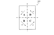
- FIG. 11 is a diagram showing an alignment division structure of a pixel 1001 in a 4D-RTN mode liquid crystal display device.
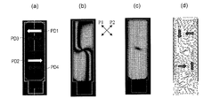
- (A), (b), and (c) are the figures for demonstrating the method for obtaining the orientation division structure of the pixel 1001 shown in FIG.
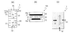
- FIG. 3 is a diagram showing an alignment division structure of a pixel 1 in the liquid crystal display device 100.
- (A), (b), and (c) are the figures for demonstrating the method for obtaining the orientation division structure of the pixel 1 shown in FIG.
- FIG. 4 is a diagram for explaining the reason why four liquid crystal domains are formed in the pixel 1 of the liquid crystal display device 100.
- FIG. (A) And (b) is a figure for demonstrating the reason why four liquid crystal domains are formed in the pixel 1 of the liquid crystal display device 100.
- FIG. (A), (b), and (c) are the figures for demonstrating the reason why four liquid crystal domains are formed in the pixel 1 of the liquid crystal display device 100.
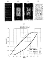
- FIG. (A)-(e) is a figure for demonstrating the result of the orientation simulation about Example 1, and an optical simulation.
- (A)-(e) is a figure for demonstrating the result of the orientation simulation about Example 2, and an optical simulation.
- (A)-(e) is a figure for demonstrating the result of the orientation simulation about Example 3, and an optical simulation.
- (A)-(e) is a figure for demonstrating the result of the orientation simulation about Example 4, and an optical simulation.
- (A)-(e) is a figure for demonstrating the result of the orientation simulation about Example 5, and an optical simulation.
- (A)-(e) is a figure for demonstrating the result of the orientation simulation about Example 6, and an optical simulation.
- (A)-(e) is a figure for demonstrating the result of the orientation simulation about the comparative example 1, and an optical simulation.
- (A), (b) and (c) is a figure which shows the orientation distribution in the pixel in the comparative example 1, Example 6, and Example 2, respectively.
- (A) and (b) show the relationship between the gradation and the luminance (standardized luminance) in Example 7 and Comparative Example 2, respectively, when observed from the front direction, when viewed from the 60 ° oblique direction, and up and down.
- (A) And (b) is sectional drawing and the top view which show typically one pixel of the liquid crystal display device 900 of CPA mode, (c) is a white voltage to the liquid crystal layer 930 of the liquid crystal display device 900. It is a figure which shows the simulation result of the transmittance
- (A), (b) and (c) is a figure for demonstrating the result of having verified formation of the defective tilt area
- FIG. 10 is an optical microscope image corresponding to one pixel 1 in Example 7.
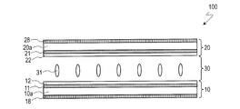
- FIG. 1 shows a liquid crystal display device 100 according to this embodiment.
- FIG. 1 is a cross-sectional view schematically showing the liquid crystal display device 100.
- the liquid crystal display device 100 includes an active matrix substrate (first substrate) 10 and a counter substrate (second substrate) 20 that are arranged to face each other, and an active matrix substrate 10 and a counter substrate 20. And a liquid crystal layer 30 provided therebetween.
- the liquid crystal display device 100 further includes a plurality of pixels arranged in a matrix.
- the plurality of pixels include a red pixel that displays red, a green pixel that displays green, and a blue pixel that displays blue, and one color display by three pixels of the red pixel, the green pixel, and the blue pixel.
- a pixel is constructed.
- An active matrix substrate (also referred to as “TFT substrate”) 10 includes a pixel electrode 11 provided in each of a plurality of pixels, and a first photo-alignment film 12 provided between the pixel electrode 11 and the liquid crystal layer 30. .
- the pixel electrode 11 and the first photo-alignment film 12 are supported by an insulating transparent substrate (for example, a glass substrate) 10a.
- the active matrix substrate includes a thin film transistor (TFT) electrically connected to the pixel electrode 11, a scanning wiring (gate bus line) for supplying a scanning signal to the TFT, and a display signal to the TFT.
- the counter substrate 20 also referred to as “color filter substrate”) 20 includes a counter electrode 21 facing the pixel electrode 11 and a second photo-alignment film 22 provided between the counter electrode 21 and the liquid crystal layer 30.
- the counter electrode 21 and the second photo-alignment film 22 are supported by an insulating transparent substrate (for example, a glass substrate) 20a.
- the counter substrate 20 has a color filter layer.
- the color filter layer includes a red color filter provided corresponding to the red pixel, a green color filter provided corresponding to the green pixel, and a blue color filter provided corresponding to the blue pixel. .
- the liquid crystal layer 30 is a vertical alignment type liquid crystal layer including liquid crystal molecules 31 having negative dielectric anisotropy. In a state where no voltage is applied to the liquid crystal layer 30, the liquid crystal molecules 31 are aligned substantially perpendicular to the substrate surface, as shown in FIG.
- the liquid crystal display device 100 further includes a pair of linearly polarizing plates 18 and 28 facing each other with at least the liquid crystal layer 30 interposed therebetween.
- the linearly polarizing plates 18 and 28 are arranged so that their transmission axes are substantially orthogonal to each other. That is, the linearly polarizing plates 18 and 28 are arranged in crossed Nicols.
- a pair of circularly polarizing plates may be provided. That is, the light incident on the liquid crystal layer 30 may be linearly polarized light or circularly polarized light.
- Each of the first photo-alignment film 12 and the second photo-alignment film 22 is a vertical alignment film that has been subjected to a photo-alignment process, and defines the pretilt direction of the liquid crystal molecules 31.
- the first photo-alignment film 12 has two regions that define different pretilt directions in each pixel.
- the second photo-alignment film 22 has two regions that define different pretilt directions in each pixel.
- FIG. 2 shows an alignment division structure of the pixel 1001 in a general 4D-RTN mode liquid crystal display device.
- four liquid crystal domains A, B, C, and D are formed in the pixel 1001 as shown in FIG.
- the four liquid crystal domains A, B, C and D are arranged in a matrix of 2 rows and 2 columns.
- the orientations of the directors t1, t2, t3, and t4 of the liquid crystal domains A, B, C, and D are four orientations in which the difference between any two directions is substantially equal to an integral multiple of 90 °.
- Directors t1, t2, t3 and t4 represent the orientation directions of the liquid crystal molecules contained in each liquid crystal domain. In the 4D-RTN mode, the directors t1, t2, t3 and t4 This is the tilt direction of the liquid crystal molecules near the center in the thickness direction.
- Each liquid crystal domain is characterized by the director orientation (tilt direction described above), and the director orientation has a dominant influence on the viewing angle dependency of each domain.
- the pair of polarizing plates facing each other through the liquid crystal layer are arranged so that the transmission axes (polarization axes) are orthogonal to each other. More specifically, one transmission axis is on the display surface. It is arranged so that it is parallel to the horizontal direction and the other transmission axis is parallel to the vertical direction of the display surface.
- the orientation of the director t1 of the liquid crystal domain A is about 225 °
- the orientation of the director t2 of the liquid crystal domain B is about 315 °
- the liquid crystal domain C The direction of the director t3 is about 45 °
- the direction of the director t4 of the liquid crystal domain D is about 135 °.
- the liquid crystal domains A, B, C, and D are arranged so that the direction of each director differs by approximately 90 ° between adjacent liquid crystal domains.
- FIG. 3A shows the pretilt directions PD1 and PD2 defined by the photo-alignment film provided on the active matrix substrate
- FIG. 3B is defined by the photo-alignment film provided on the counter substrate.
- the pretilt directions PD3 and PD4 are shown.
- FIG. 3C shows a tilt direction (director) when a voltage is applied to the liquid crystal layer.
- the region on the active matrix substrate side (region corresponding to one pixel 1001) is divided into left and right parts, and the photo-alignment film in each region (left region and right region) Photo-alignment processing is performed so that the (vertical alignment film) defines the pretilt directions PD1 and PD2 that are antiparallel to each other.
- the photo-alignment process is performed by obliquely irradiating ultraviolet rays from the direction indicated by the arrow.
- the area on the counter substrate side (area corresponding to one pixel area 1001) is vertically divided into two areas, and each area (upper area and lower area) is divided.
- the photo-alignment process is performed so that the photo-alignment film (vertical alignment film) defines the pretilt directions PD3 and PD4 that are antiparallel to each other.
- the photo-alignment process is performed by obliquely irradiating ultraviolet rays from the direction indicated by the arrow.
- the active matrix substrate and the counter substrate that have been subjected to the photo-alignment treatment are bonded to each other, thereby forming an alignment-divided pixel 1001 as shown in FIG. be able to.
- the pretilt direction defined by the photo-alignment film of the active matrix substrate and the photo-alignment film of the counter substrate are defined.
- the pretilt direction differs from the pretilt direction by approximately 90 °, and the tilt direction (the direction of the director of each liquid crystal domain) is defined in the middle of the two pretilt directions.
- the ultraviolet irradiation is performed from different directions.
- an area where a sufficient pretilt angle cannot be provided around the exposure seam (the boundary between two areas having different pretilt directions) due to light diffraction. (Hereinafter referred to as “defective tilt region”).
- the “pretilt angle” refers to an angle formed by the major axis of the liquid crystal molecules 31 with respect to the normal direction of the substrate surface when no voltage is applied.
- each pixel 1001 includes a portion extending in the vertical direction (corresponding to the defective tilt region NGR1) and a portion extending in the horizontal direction (corresponding to the defective tilt region NGR2).
- a cross-shaped defective tilt region NGR is formed.
- FIG. 4 shows an alignment division structure of the pixel 1 in the liquid crystal display device 100.
- the orientation of the director t1 of the liquid crystal domain A is about 270 °
- the orientation of the director t2 of the liquid crystal domain B is about 0 °
- the liquid crystal domain C The direction of the director t3 is approximately 90 °
- the direction of the director t4 of the liquid crystal domain D is approximately 180 °. That is, the difference between any two of the four director directions of the liquid crystal domains A, B, C, and D is substantially equal to an integral multiple of 90 °.
- the transmission axes (polarization axes) P1 and P2 of the pair of linearly polarizing plates 18 and 28 form an angle of approximately 45 ° with the orientations of the directors t1, t2, t3, and t4 of the liquid crystal domains A, B, C, and D.
- the transmission axes P1 and P2 of the pair of linearly polarizing plates 18 and 28 are approximately 45 ° in both the pretilt direction defined by the first photoalignment film 12 and the second photoalignment film 22. The corner of the.
- FIG. 4 illustrates a case where the areas occupied by the four liquid crystal domains A, B, C, and D in the pixel 1 are equal to each other, but the areas of the four liquid crystal domains A, B, C, and D are as follows. It does not have to be equal to each other. However, from the viewpoint of uniformity of viewing angle characteristics, it is preferable that the difference in area between the four liquid crystal domains A, B, C, and D is as small as possible. Specifically, the four liquid crystal domains A, B, C, and The difference between the area of the largest liquid crystal domain in D and the area of the smallest liquid crystal domain is preferably 50% or less of the largest area.
- the example shown in FIG. 4 is an example of the most preferable (ie, ideal) quadrant structure in view angle characteristics.
- FIG. 5A shows the pretilt directions PD1 and PD2 defined by the first photo-alignment film 12 provided on the active matrix substrate 10
- FIG. 5B shows the first tilt direction provided on the counter substrate 20.
- the pretilt directions PD3 and PD4 defined by the two-light alignment film 22 are shown.
- FIG. 5C shows the tilt direction (director) when a voltage is applied to the liquid crystal layer 30.
- the first photo-alignment film 12 includes a first pretilt region 12a that defines the first pretilt direction PD1 and a second antiparallel to the first pretilt direction PD1. And a second pretilt region 12b that defines a pretilt direction PD2.
- the region corresponding to one pixel 1 of the first photo-alignment film 12 is divided into two vertically, and the respective regions (first pretilt region and second pretilt region) 12a and 12b are opposite to each other.
- Photo-alignment processing is performed so as to define parallel pretilt directions (first pretilt direction and second pretilt direction) PD1 and PD2.
- the photo-alignment treatment is performed by obliquely irradiating ultraviolet rays from the direction indicated by the arrow.
- the second photo-alignment film 22 is antiparallel to the third pretilt direction PD3 and the third pretilt region 22a that defines the third pretilt direction PD3, as shown in FIG. And a fourth pretilt region 22b that defines a fourth pretilt direction PD4.
- the region corresponding to one pixel 1 of the second photo-alignment film 22 is divided into two vertically, and the respective regions (third pre-tilt region and fourth pre-tilt region) 22a and 22b are opposite to each other.
- Photo-alignment processing is performed so as to define the parallel pretilt directions (third pretilt direction and fourth pretilt direction) PD3 and PD4.
- the photo-alignment treatment is performed by obliquely irradiating ultraviolet rays from the direction indicated by the arrow.
- the third pre-tilt region 22a of the second photo-alignment film 22 is the first pre-alignment film 12 of the first photo-alignment film 12 when viewed from the normal direction of the display surface.
- the fourth pretilt region 22 b of the second photo-alignment film 22 overlaps (opposites) the second pre-tilt region 12 b of the first photo-alignment film 12.
- the third pretilt direction PD3 is antiparallel to the first pretilt direction PD1
- the fourth pretilt direction PD4 is antiparallel to the second pretilt direction PD2. It is.
- the active matrix substrate 10 and the counter substrate 20 that have been subjected to the photo-alignment treatment are bonded to each other, whereby the pixel 1 that has undergone the alignment division as shown in FIG. Can be formed.
- the voltage is applied when the voltage is applied. It seems that only two liquid crystal domains are formed as in the pixel 1 ′ shown in FIG. However, for the reason described later, actually, as shown in FIG. 5C, four liquid crystal domains A, B, C, and D are formed.
- the periphery of the boundary BD1 between the first pre-tilt region 12a and the second pre-tilt region 12b of the first photo-alignment film 12 can be a defective tilt region NGR1 that cannot provide a sufficient pre-tilt angle (see FIG. 5A). Further, the periphery of the boundary BD2 between the third pre-tilt region 22a and the fourth pre-tilt region 22b of the second photo-alignment film 22 can be a defective tilt region NGR2 to which a sufficient pre-tilt angle cannot be given. However, in the liquid crystal display device 100 according to the present embodiment, as shown in FIG.
- the first pre-tilt region 12a and the second pre-tilt region 12b of the first photo-alignment film 12 are viewed from the normal direction of the display surface.
- the entire boundary BD1 and the entire boundary BD2 of the third pre-tilt region 22a and the fourth pre-tilt region 22b of the second photo-alignment film 22 overlap.
- the defective tilt region NGR1 on the first photo-alignment film 12 side and the defective tilt region NGR2 on the second photo-alignment film 22 side overlap, and as shown in FIG. A defective tilt NGR extending only in the horizontal direction is formed.
- the area of the defective tilt region NGR can be reduced as compared with the pixel 1001 shown in FIG. For this reason, it is possible to suppress a decrease in average pretilt angle in the entire pixel 1 (due to the defective tilt region NGR), so that the alignment state of the liquid crystal molecules 31 is sufficiently stabilized and a sufficient response speed is realized. be able to.
- an active matrix substrate 10 having a first photo-alignment film 12 is prepared. This step can be performed by a method similar to a method of manufacturing a general active matrix substrate for 4D-RTN mode.
- a second pretilt region 12b that defines the pretilt direction PD2 is formed by a photo-alignment process.
- This step includes, for example, a step of irradiating light to a portion to be the first pretilt region 12a in a state where the portion to be the second pretilt region 12b of the first photo-alignment film 12 is shielded by the photomask, Irradiating light to a portion to be the second pretilt region 12b in a state where the first pretilt region 12a of the first photo-alignment film 12 is shielded by the photomask.
- the light irradiation may be performed on the portion to be the second pretilt region 12b before the light irradiation is performed on the portion to be the first pretilt region 12a.
- a counter substrate 20 having a second photo-alignment film 22 is prepared separately from the active matrix substrate 10. This step can be performed by a method similar to a method for manufacturing a common counter substrate for 4D-RTN mode.
- a third pretilt region 22a that defines the third pretilt direction PD3 in a region corresponding to each of the plurality of pixels 1 of the second photoalignment film 22, and a fourth antiparallel to the third pretilt direction PD3.
- a fourth pretilt region 22b that defines the pretilt direction PD4 is formed by a photo-alignment process.
- This step includes, for example, a step of irradiating light to a portion to be the third pretilt region 22a in a state where the portion to be the fourth pretilt region 22b of the second photo-alignment film 22 is shielded by the photomask, And irradiating light onto a portion that becomes the fourth pretilt region 22b in a state where the third pretilt region 22a of the second photo-alignment film 22 is shielded by the photomask.
- the light irradiation may be performed on the portion to be the fourth pretilt region 22b before the light irradiation is performed on the portion to be the third pretilt region 22a.
- the counter substrate 20 thus bonded is bonded.
- a liquid crystal layer 30 is formed by injecting a liquid crystal material between the active matrix substrate 10 and the counter substrate 20 using, for example, a vacuum injection method.
- the liquid crystal layer 30 may be formed by a dropping method (that is, by applying a liquid crystal material on one substrate before bonding).
- the process of performing the photo-alignment process on the first photo-alignment film 12 and the process of performing the photo-alignment process on the second photo-alignment film 22 are performed in the normal direction of the display surface when the active matrix substrate 10 and the counter substrate 20 are bonded together.
- the entire boundary BD1 between the first pretilt region 12a and the second pretilt region 12b of the first photo-alignment film 12, and the entire boundary BD2 between the third pre-tilt region 22a and the fourth pretilt region 22b of the second photo-alignment film 22 are viewed. Are executed so that they overlap.
- a process of performing a realignment process including a heat process on the liquid crystal layer 30 may be performed.
- This realignment treatment can eliminate the alignment disorder (fluid alignment) that occurs when the liquid crystal material is injected.
- the liquid crystal display device 100 of the present embodiment is obtained by performing a process of attaching the pair of linearly polarizing plates 18 and 28 to the outside of the active matrix substrate 10 and the counter substrate 20.
- liquid crystal display device 100 of this embodiment when only the alignment regulating force of the first photo-alignment film 12 and the second photo-alignment film 22 is considered, only two liquid crystal domains are applied when a voltage is applied. In fact, four liquid crystal domains A, B, C and D are formed, which provides sufficiently high viewing angle characteristics. In particular, when the screen resolution is 200 ppi or more, as will be described in detail later, viewing angle characteristics substantially equivalent to those of a general 4D-RTN mode can be obtained.
- FIGS. 7A to 7D are diagrams regarding the pixel 1001 in the 4D-RTN mode
- FIGS. 8A to 8D are diagrams regarding the pixel 1 of the liquid crystal display device 100 according to the present embodiment. is there.
- FIGS. 7A to 7D are diagrams regarding the pixel 1001 in the 4D-RTN mode
- FIGS. 8A to 8D are diagrams regarding the pixel 1 of the liquid crystal display device 100 according to the present embodiment. is there.
- FIGS. 7A and 8A are calculation mask diagrams, which are defined by the pretilt directions PD1 and PD2 defined by the photo-alignment film on the active matrix substrate side and the photo-alignment film on the counter substrate side.
- the pretilt directions PD3 and PD4 are also shown.
- FIGS. 7B and 8B are diagrams showing simulation results of transmittance when a linearly polarizing plate arranged so that the transmission axes P1 and P2 are substantially orthogonal to each other is used as the polarizing plate.
- FIG.7 (c) and FIG.8 (c) are figures which show the simulation result of the transmittance
- FIG. 7D and FIG. 8D are diagrams showing the orientation distribution in the pixel, and the orientation direction of rough liquid crystal molecules (which may be called the director orientation) in each liquid crystal domain is indicated by an arrow. It is shown.
- the calculation conditions for the orientation simulation are
- the shape of the pixel electrode and the like is substantially the same in the pixel 1001 in the 4D-RTN mode and the pixel 1 of the present embodiment.
- the 4D-RTN mode pixel 1001 In the case of using the linear polarizing plate, the 4D-RTN mode pixel 1001 generates a saddle-shaped dark line characteristic of the 4D-RTN mode, as shown in FIG. 7B.
- the generation location is slightly different from the dark line of the pixel 1001 in the 4D-RTN mode, a dark line having substantially the same shape is generated. Therefore, it is considered that the 4D structure is also formed in the pixel 1 of the present embodiment.
- the liquid crystal molecules are roughly aligned in four directions in both the 4D-RTN mode pixel 1001 and the pixel 1 of the present embodiment. It was confirmed that
- the outer edge of the pixel electrode 11 includes a first edge portion 11e1 and a second edge portion 11e2.
- the first edge portion 11e1 is close to the liquid crystal domain A
- the second edge portion 11e2 is close to the liquid crystal domain C.
- the direction e1 orthogonal to the first edge portion 11e1 and going inward of the pixel electrode 11 is the direction opposite to the first pretilt direction PD1.
- a direction e2 that is orthogonal to the second edge portion 11e2 and goes inward of the pixel electrode 11 is a direction opposite to the second pretilt direction PD2.
- the outer edge of the pixel electrode 11 includes the first edge portion 11e1 and the second edge portion 11e2 as described above, four liquid crystal domains are formed when a voltage is applied. Hereinafter, this reason will be described in more detail with reference to FIGS. 10 and 11.
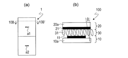
- FIG. 10A is a plan view showing one pixel 1.
- the alignment regulating force by the first photo-alignment film 12 and the second photo-alignment film 22 is indicated by solid arrows a1, a2.
- FIG. 10B is a cross-sectional view taken along the line 10B-10B 'in FIG. 10A, and shows the alignment state of the liquid crystal molecules 31 when no voltage is applied.
- the liquid crystal molecules 31 when no voltage is applied, the liquid crystal molecules 31 have a predetermined angle (pretilt) in a predetermined direction by the alignment regulating forces a1 and a2 by the first photoalignment film 12 and the second photoalignment film 22. Pretilt at (angle) ⁇ .
- the liquid crystal molecules 31 are tilted to the left with respect to the normal direction of the substrate surface.
- FIG. 11A is a plan view showing one pixel 1, and FIG. 11A shows not only the alignment regulating forces a1 and a2 by the first photo-alignment film 12 and the second photo-alignment film 22, but also The alignment regulating force due to the oblique electric field generated in the vicinity of the outer edge of the pixel electrode 11 is indicated by broken arrows b1, b2, b3, and b4.
- FIG. 11B is a cross-sectional view taken along the line 11B-11B ′ in FIG. 11A, and shows the alignment state of the liquid crystal molecules 31 when a voltage is applied (however, the first photo-alignment film 12 and the second photo-alignment film 12).
- the alignment regulating forces a1 and a2 by the photo-alignment film 22 are not considered).
- FIG. 11B when a voltage is applied, the liquid crystal molecules 31 having negative dielectric anisotropy are aligned so as to be perpendicular to the electric lines of force E. Therefore, in the vicinity of the outer edge of the pixel electrode 11, there are alignment regulating forces (alignment regulating forces b1, b2, b3, and b4 shown in FIG. 11A) that tilt the liquid crystal molecules 31 toward the inside of the pixel electrode 11. To do.
- the first photo alignment film 12 and the second photo alignment film 22 are used.
- the direction of the alignment regulating force due to (which is the direction coinciding with the first pretilt direction PD1 and the second pretilt direction PD2) and the direction of the alignment regulating force due to the oblique electric field (inside the edge of the pixel electrode 11 and inside the pixel electrode 11) Is the opposite direction).
- FIG. 11C shows an enlarged lower right portion of the pixel 1.
- the liquid crystal molecules 31 are tilted upward (direction c). .
- the alignment regulating force a1 by the first photo-alignment film 12 and the second photo-alignment film 22 competes with the alignment regulating forces b1 and b4 by the oblique electric field. Falls to the side.
- the liquid crystal molecules 31 are aligned in the direction perpendicular to the display surface (approximately 270 ° direction and approximately 90 ° direction) when a voltage is applied. Oriented to Therefore, four liquid crystal domains A, B, C, and D having different director directions are formed in the pixel 1.
- liquid crystal display device 100 since the four liquid crystal domains A, B, C, and D are actually formed in each pixel 1 when a voltage is applied, sufficiently high viewing angle characteristics are obtained. It is done.
- orientation simulation and optical simulation performed at various screen resolutions (pixel pitches) will be described.
- Example 1 a liquid crystal display device having the pixel 1001 shown in FIG.
- the screen resolution and pixel pitch (pixel size) of Examples 1 to 6 and Comparative Example 1 are as shown in Table 2 below.
- a region where exposure is performed overlapping the photo-alignment film (exposure overlap region) with a width of 20 ⁇ m is formed at the center of the pixel, and the pretilt angle at the center of the exposure overlap region is 0 °. .
- the white voltage maximum gradation voltage was set to 3.9 V based on the actually measured value of the 4.18 type panel actually manufactured.
- FIGS. 12 corresponds to the first embodiment
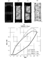
- FIG. 13 corresponds to the second embodiment
- FIG. 14 corresponds to the third embodiment
- 15 corresponds to the fourth embodiment
- FIG. 16 corresponds to the fifth embodiment
- FIG. 17 corresponds to the sixth embodiment
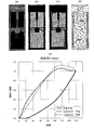
- FIG. 18 corresponds to the first comparative example.
- FIG. 12 to FIG. 18 is a mask diagram for calculation.
- B in FIG. 12 to FIG. 18 is a diagram showing a simulation result of transmittance when a circularly polarizing plate is used as the polarizing plate.
- C in FIGS. 12 to 18 is a diagram showing a simulation result of transmittance when a linearly polarizing plate arranged so that the transmission axes are substantially orthogonal to each other is used as the polarizing plate.
- D in FIG. 12 to FIG. 18 is a diagram showing the orientation distribution in the pixel, and the orientation direction of rough liquid crystal molecules (which may be called the director orientation) in each liquid crystal domain is indicated by an arrow. Has been.
- E in FIG. 12 to FIG.
- FIG. 18 shows the relationship between the gradation and the luminance (luminance normalized with the luminance in the white display state set to 1), the front direction, and the right 60 ° direction (rightward viewing angle).
- FIG. 6 is a graph showing a 60 ° tilted direction and a 60 ° tilted direction (a direction in which the viewing angle is tilted 60 ° upward), and a ⁇ characteristic (luminance level) when compared to when viewed from the front direction when viewed from an oblique direction. This represents how much the key dependency shifts.
- Example 6 in which the screen resolution is the same as that of Comparative Example 1, the luminance in the observation from the right diagonal 60 ° direction and the observation from the upper diagonal 60 ° direction is shown. The difference is larger than that of Comparative Example 1.
- Example 6 Although the screen resolution of Example 6 is lower than that of Example 5, the difference in luminance between the observation from the diagonally right 60 ° direction and the observation from the diagonally upper 60 ° direction is that of Example 5. Although it is smaller than this, in Example 6, it is considered that the calculation was performed with a pattern in which the inside of the pixel was partially shielded.
- FIGS. 19A, 19B, and 19C are diagrams showing the orientation distribution in the pixels for Comparative Example 1, Example 6, and Example 2, respectively, and FIGS. ) And FIG. 13 (d) are enlarged.
- the liquid crystal molecules are in the lower left direction (approximately 225 ° direction), the lower right direction (approximately 315 ° direction), the upper right direction (approximately 45 ° direction), and the upper left direction (approximately Four regions oriented in the direction of 135 ° occupy most of the pixels.
- the region where the liquid crystal molecules are oriented in the downward direction (approximately 270 ° direction) and the upward direction (approximately 90 ° direction) is present on the upper left side and the lower right side of the pixel, small.
- the liquid crystal molecules are aligned in approximately four directions in the pixel, and the four regions in which the liquid crystal molecules are aligned in the lower left direction, the lower right direction, the upper right direction, and the upper left direction dominate in terms of optical characteristics. Is.
- Example 6 the two regions in which the liquid crystal molecules are aligned in the left direction (approximately 180 ° direction) and the right direction (approximately 0 ° direction) are the majority of the pixels. Accounted for. Although the region where the liquid crystal molecules are oriented in the downward direction (approximately 270 ° direction) and the upward direction (approximately 90 ° direction) is present on the upper left side and the lower right side of the pixel, small. Therefore, it can be considered that the liquid crystal molecules are aligned in approximately two directions within the pixel, and two regions in which the liquid crystal molecules are aligned in the left direction and the right direction are dominant in terms of optical characteristics.
- Example 2 As can be seen from FIG. 19C, the ratio of the liquid crystal molecules in the pixel aligned in the downward direction and the upward direction in the pixel is higher than that in Example 6. Therefore, it can be considered that the liquid crystal molecules are aligned in approximately four directions in the pixel, and the four regions in which the liquid crystal molecules are aligned in the downward direction, the right direction, the upward direction, and the left direction (shown in FIG. 4 and the like).
- Four liquid crystal domains A, B, C and D) dominate in terms of optical properties.
- the screen resolution is 200 ppi or more (the shorter one of the pixel pitch along the display surface horizontal direction and the pixel pitch along the display surface vertical direction is 42 ⁇ m or less)
- the difference between the liquid crystal domain with the largest area and the liquid crystal domain with the smallest area can be reduced to a certain extent (specifically, 50% or less), which is inferior to that of a general 4D-RTN mode liquid crystal display device. It was found that sufficiently high viewing angle characteristics can be obtained.
- Example 7 a liquid crystal display device 100 with a screen resolution of 217 ppi is actually manufactured as Example 7 and the results of measuring various characteristics will be described.
- a 4D-RTN mode liquid crystal display device having a screen resolution of 217 ppi was manufactured as a prototype, and as a comparative example 3, a CPA (Continuous Pinwheel Alignment) mode liquid crystal display device having a screen resolution of 217 ppi was manufactured.
- the results of measuring various characteristics will also be described.
- the CPA mode is a kind of VA mode, and is disclosed in, for example, Japanese Patent Application Laid-Open Nos. 2003-43525 and 2002-202511.
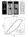
- Example 7 The results of measuring transmittance and response speed for Example 7, Comparative Example 2 and Comparative Example 3 are shown in Table 3 below.
- Table 3 As the response speed, the rising response time Tr when the display gradation is changed from 0 gradation to 32 gradation at 25 ° C. and the falling response time T d when changing the gradation from 32 gradation to 0 gradation. Is shown.
- Table 3 also shows the heat treatment temperature and the pretilt angle (average pretilt angle) in the realignment treatment step for Example 7 and Comparative Example 2.
- Example 7 two liquid crystal display devices 100 having different heat treatment temperatures were manufactured as prototypes.
- the rise response time Tr is longer in the comparative example 2 (4D-RTN mode) than the comparative example 3 (CPA mode), and is twice or more. This is considered to be caused by the fact that the average pretilt angle is reduced by increasing the ratio of the defective tilt region in the pixel as described above.
- Example 7 the rise response time substantially equivalent to that of Comparative Example 3 is realized. This is considered to be because the decrease in the average pretilt angle is suppressed as described above.
- Example 7 a higher transmittance than that of Comparative Example 3 is realized.
- an alignment regulating means (a protrusion formed from a dielectric or an opening formed in the counter electrode) is provided on the counter substrate side to stabilize the alignment by fixing the center of the axially symmetric alignment. In many cases, this orientation regulating means causes a decrease in transmittance.
- the liquid crystal display device 100 of this embodiment does not require such an alignment control means, it can implement
- Example 20 (a) and 20 (b) show the relationship between the gradation and the luminance (standardized luminance) in Example 7 and Comparative Example 2 when observed from the front direction, when observed from the 60 ° oblique direction, and It shows about the time of observation from 60 degrees up and down diagonal directions.
- FIGS. 20A and 20B in Example 7, as in Comparative Example 2, the azimuth angle dependency of the ⁇ shift was small, and sufficiently high viewing angle characteristics were obtained. Although not shown here, the same viewing angle characteristics as in Comparative Example 2 were obtained in Comparative Example 3.
- the heat treatment is preferably performed at 110 ° C. or lower.
- the nematic phase-isotropic phase transition temperature of the liquid crystal material is T NI
- the effect of the realignment treatment may not be sufficiently obtained at a temperature lower than T NI + 10 ° C. NI + 10 ° C. or higher is preferable.
- the pre-tilt angle is given by the photo-alignment film (the pre-tilt direction is defined) because the photo-functional group is formed when the photo-alignment film (typically formed from a polyimide-based material) is irradiated with ultraviolet rays. It is thought that the side chain is directed to the incident side of ultraviolet rays by the photoreaction. However, since this reaction is reversible with respect to heat, if the heat treatment in the reorientation treatment process is performed at a high temperature for a long time, the original pretilt angle (before the photoalignment treatment) (0 °: based on the substrate surface) If it does, it will return to 90 °). Therefore, it is considered preferable to perform the heat treatment at a lower temperature.
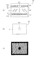
- FIGS. 21A and 21B are a cross-sectional view and a plan view schematically showing one pixel of the CPA mode liquid crystal display device 900.
- FIG. 21A and 21B are a cross-sectional view and a plan view schematically showing one pixel of the CPA mode liquid crystal display device 900.
- the liquid crystal display device 900 includes an active matrix substrate 910 and a counter substrate 920 arranged so as to face each other, and a vertical alignment type liquid crystal layer 930 provided therebetween.
- the active matrix substrate 910 includes a pixel electrode 911 provided in each pixel and a vertical alignment film 912 provided between the pixel electrode 911 and the liquid crystal layer 930.
- the pixel electrode 911 and the vertical alignment film 912 are supported by the transparent substrate 910a.
- the counter substrate 920 includes a counter electrode 921 that faces the pixel electrode 911 and a vertical alignment film 922 provided between the counter electrode 921 and the liquid crystal layer 930.
- the counter electrode 921 and the vertical alignment film 922 are supported by the transparent substrate 920a.
- the counter electrode 921 has an opening 921 a formed in a region facing substantially the center of the pixel electrode 911.
- the liquid crystal molecules 931 are axially symmetrically aligned.
- the opening 921a of the counter electrode 921 functions to fix the center of the axially symmetric orientation and stabilize the orientation.
- a protrusion sometimes referred to as a rivet
- FIG. 21C shows a simulation result of transmittance when a white voltage is applied to the liquid crystal layer 930 of the liquid crystal display device 900 (including a circularly polarizing plate as a polarizing plate). As can be seen from FIG. 21C, the region corresponding to the opening 921a of the counter electrode 921 is dark, and the luminance is lowered.
- the size of the orientation regulating means itself in the case of the opening 921a formed in the counter electrode 921, it is generally about 10 ⁇ m in diameter.
- the size of the orientation regulating means is reduced, there is a possibility that the orientation state cannot be sufficiently stabilized due to insufficient orientation regulating force.
- new equipment such as a high-resolution stepper device in order to form fine alignment regulating means.
- the size of the orientation regulating means cannot be reduced below a certain level. Therefore, when the pixel pitch is reduced with the increase in definition, the ratio of the orientation regulating means for fixing the center to the entire pixel increases.
- the CPA mode is currently often used in small and medium-sized liquid crystal display devices, but for the reasons described above, in the CPA mode liquid crystal display device, the brightness decreases as the pixel pitch decreases as the definition increases. Resulting in.
- liquid crystal display device 100 particularly when a circularly polarizing plate is used as the polarizing plate, as shown in FIG. be able to.
- the response speed is improved in the liquid crystal display device 100 according to the present embodiment because the area of the defective tilt region NGR is smaller than that in the 4D-RTN mode liquid crystal display device.
- the inventor of the present application verified whether or not the defective tilt region NGR is actually formed by the diffraction phenomenon of light, and to what extent the defective pretilt region NGR is formed if formed. The results will be explained.
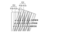
- a substrate 810 having a photo-alignment film 812 formed thereon was prepared, and the photo-alignment film 812 of the substrate 810 was irradiated with ultraviolet rays from the direction indicated by the arrow.
- FIG. 22B in a state where a partial region of the photo-alignment film 812 is shielded by the photomask in which the light shielding portions 815 are arranged in a stripe shape, the direction indicated by the arrow (FIG. 22 ( Ultraviolet rays were irradiated from the direction opposite to the direction shown in a).
- the photo-alignment film 812 is exposed to the region (first region) 812a irradiated with ultraviolet rays only once and the ultraviolet rays twice as shown in FIG.
- An irradiated region (second region) 812b was formed.
- the first region 812a is a region where a large pretilt angle (specifically, 2.5 °) can be given by ultraviolet irradiation in the first exposure step.
- the second region 812b is more strongly affected by ultraviolet irradiation in the second exposure step of the two exposure steps in which ultraviolet irradiation is performed from opposite directions, and a small pretilt angle (specifically, -0.5 °).
- the cross section of the panel obtained by bonding is configured by a region where the first regions 812a face each other and a region where the second regions 812b face each other (" A cross-section composed of only regions where the first region 812a and the second region 812b face each other (referred to as an “offset region”), and a cross-section where these regions coexist (referred to as an “intermediate region”). ) And exist.
- FIG. 24 shows a position profile along the Y direction (left-right direction in FIG. 23) of the pretilt angle for each of the emphasis region, the intermediate region, and the canceling region.
- FIG. 24 also shows the positions of the light shielding part and the light transmitting part of the photomask. Note that the pretilt angle when the entire surface exposure is performed only once without a photomask is 2.55 °.
- the pretilt angle changes from 2.5 ° to ⁇ 0.5 ° in a region having a width of about 20 to 40 ⁇ m centering on the boundary between the light shielding portion and the light transmitting portion of the photomask. .
- the entire boundary BD1 between the first pretilt region 12a and the second pretilt region 12b of the first photoalignment film 12 and the third pretilt region 22a of the second photoalignment film 22 are used.
- by reducing the area of the defective tilt region NGR by overlapping the entire boundary BD2 of the fourth pretilt region 22b, it is possible to suppress a decrease in the average pretilt angle in the entire pixel 1.
- FIGS. 25A and 25B show the positions in the pixel 1 when the temperature of the heat treatment in the reorientation treatment step is 110 ° C. and 130 ° C. (both times are 40 minutes), respectively.
- 5 is a graph showing the relationship between the angle and the pretilt angle.
- shaft of the graph of Fig.25 (a) and (b) is a tilt angle with respect to a substrate surface.
- the pretilt angle was measured along the direction Y shown in FIG.
- FIG. 26 is an optical microscope image corresponding to one pixel 1.
- an area having a width of about 20 ⁇ m centered on the boundary between the pretilt areas is an area where a sufficient pretilt angle cannot be given (defective tilt area). It can be seen that the region can realize a sufficiently large pretilt angle.
- the first photo-alignment film 12 and the second photo-alignment film 22 are divided into two vertically in each pixel 1, and the first
- the first pretilt direction PD1, the second pretilt direction PD2, the third pretilt direction PD3, and the fourth pretilt direction PD4 are all substantially parallel to the left-right direction of the display surface is illustrated, but the orientation division mode is limited to the illustrated example. Not.
- the first photo-alignment film 12 and The second photo-alignment film 22 is divided into left and right parts in each pixel 1, and the first pretilt direction PD1, the second pretilt direction PD2, the third pretilt direction PD3, and the fourth pretilt direction PD4 are substantially parallel to the vertical direction of the display surface. It is good.
- one color display pixel is composed of three pixels, and the aspect ratio (aspect ratio) of one pixel is 3: 1.
- the pixels constituting one color display pixel are exemplified.
- the number and aspect ratio of the pixels are not limited to those exemplified here.
- a VA mode liquid crystal display device in which the pretilt direction of liquid crystal molecules is defined by a photo-alignment film, which is suitable for high definition.
Landscapes
- Physics & Mathematics (AREA)
- Nonlinear Science (AREA)
- Chemical & Material Sciences (AREA)
- Crystallography & Structural Chemistry (AREA)
- General Physics & Mathematics (AREA)
- Optics & Photonics (AREA)
- Mathematical Physics (AREA)
- Spectroscopy & Molecular Physics (AREA)
- Liquid Crystal (AREA)
Abstract
L'invention concerne un dispositif d'affichage à cristaux liquides (100) qui comporte : une couche de cristaux liquides de type à alignement vertical (30) ; un premier film de photo-alignement (12) et un second film de photo-alignement (22). Le premier film de photo-alignement présente une première région de pré-inclinaison (12a) et une deuxième région de pré-inclinaison (12b) définissant des directions de pré-inclinaison mutuellement antiparallèles (PD1, PD2). Le second film de photo-alignement présente une troisième région de pré-inclinaison (22a) et une quatrième région de pré-inclinaison (22b) définissant des directions de pré-inclinaison mutuellement antiparallèles (PD3, PD4). La frontière globale (BD1) entre la première région de pré-inclinaison et la deuxième région de pré-inclinaison et la frontière globale (BD2) entre la troisième région de pré-inclinaison et la quatrième région de pré-inclinaison se superposent l'une par rapport à l'autre lorsqu'elles sont vues dans la direction normale à la surface d'affichage.
Priority Applications (1)
| Application Number | Priority Date | Filing Date | Title |
|---|---|---|---|
| US14/899,841 US9933662B2 (en) | 2013-06-20 | 2014-02-27 | Liquid crystal display device and method for manufacturing same |
Applications Claiming Priority (2)
| Application Number | Priority Date | Filing Date | Title |
|---|---|---|---|
| JP2013-129989 | 2013-06-20 | ||
| JP2013129989 | 2013-06-20 |
Publications (1)
| Publication Number | Publication Date |
|---|---|
| WO2014203565A1 true WO2014203565A1 (fr) | 2014-12-24 |
Family
ID=52104311
Family Applications (1)
| Application Number | Title | Priority Date | Filing Date |
|---|---|---|---|
| PCT/JP2014/054961 Ceased WO2014203565A1 (fr) | 2013-06-20 | 2014-02-27 | Dispositif d'affichage à cristaux liquides et son procédé de fabrication |
Country Status (2)
| Country | Link |
|---|---|
| US (1) | US9933662B2 (fr) |
| WO (1) | WO2014203565A1 (fr) |
Families Citing this family (2)
| Publication number | Priority date | Publication date | Assignee | Title |
|---|---|---|---|---|
| CN110764315B (zh) * | 2019-10-28 | 2022-05-03 | Tcl华星光电技术有限公司 | 液晶配向力仿真方法、系统、设备及存储介质 |
| CN114879414A (zh) * | 2022-04-26 | 2022-08-09 | 成都中电熊猫显示科技有限公司 | 一种显示面板和显示装置 |
Citations (3)
| Publication number | Priority date | Publication date | Assignee | Title |
|---|---|---|---|---|
| JPH07281187A (ja) * | 1994-02-17 | 1995-10-27 | Stanley Electric Co Ltd | 液晶表示素子の製造方法 |
| JP2000131698A (ja) * | 1998-10-27 | 2000-05-12 | Stanley Electric Co Ltd | 液晶表示素子とその製造方法 |
| WO2011161921A1 (fr) * | 2010-06-23 | 2011-12-29 | シャープ株式会社 | Dispositif d'affichage à cristaux liquides |
Family Cites Families (7)
| Publication number | Priority date | Publication date | Assignee | Title |
|---|---|---|---|---|
| US5712696A (en) | 1994-02-17 | 1998-01-27 | Stanley Electric, Co., Ltd. | Manufacture of LCD device by transferring the orientation state from a parent substrate to a child substrate |
| TW589504B (en) | 1997-06-12 | 2004-06-01 | Sharp Kk | Liquid crystal display device |
| JP3601786B2 (ja) | 2000-08-11 | 2004-12-15 | シャープ株式会社 | 液晶表示装置 |
| JP3601788B2 (ja) | 2000-10-31 | 2004-12-15 | シャープ株式会社 | 液晶表示装置 |
| JP4666398B2 (ja) | 2005-05-13 | 2011-04-06 | シャープ株式会社 | 液晶表示装置 |
| US7995177B2 (en) | 2005-06-09 | 2011-08-09 | Sharp Kabushiki Kaisha | Liquid crystal display device |
| CN105705988A (zh) * | 2013-10-21 | 2016-06-22 | 夏普株式会社 | 液晶显示装置 |
-
2014
- 2014-02-27 WO PCT/JP2014/054961 patent/WO2014203565A1/fr not_active Ceased
- 2014-02-27 US US14/899,841 patent/US9933662B2/en active Active
Patent Citations (3)
| Publication number | Priority date | Publication date | Assignee | Title |
|---|---|---|---|---|
| JPH07281187A (ja) * | 1994-02-17 | 1995-10-27 | Stanley Electric Co Ltd | 液晶表示素子の製造方法 |
| JP2000131698A (ja) * | 1998-10-27 | 2000-05-12 | Stanley Electric Co Ltd | 液晶表示素子とその製造方法 |
| WO2011161921A1 (fr) * | 2010-06-23 | 2011-12-29 | シャープ株式会社 | Dispositif d'affichage à cristaux liquides |
Also Published As
| Publication number | Publication date |
|---|---|
| US9933662B2 (en) | 2018-04-03 |
| US20160139466A1 (en) | 2016-05-19 |
Similar Documents
| Publication | Publication Date | Title |
|---|---|---|
| CN102116965B (zh) | 液晶显示装置 | |
| JP5881057B2 (ja) | 横電界方式の液晶表示装置及びその製造方法 | |
| US8525965B2 (en) | Liquid crystal display panel with unit pixels having slits in pixel electrode and photo alignment layers | |
| JP6347937B2 (ja) | 液晶表示装置 | |
| JP5209754B2 (ja) | 液晶表示装置 | |
| US20120229739A1 (en) | Liquid crystal display device and manufacturing method therefor | |
| KR20150012093A (ko) | 액정 표시 장치 및 그 제조 방법 | |
| WO2013054828A1 (fr) | Affichage à cristaux liquides | |
| JPWO2009122864A1 (ja) | カラーフィルタ基板及び液晶表示装置 | |
| WO2010119659A1 (fr) | Dispositif d'affichage à cristaux liquides | |
| US10718978B2 (en) | Apparatus for improving optical alignment of panels manufactured on a same mother substrate | |
| WO2015060001A1 (fr) | Dispositif d'affichage à cristaux liquides | |
| WO2011013649A1 (fr) | Dispositif d'affichage à cristaux liquides et procédé de fabrication de celui-ci | |
| WO2012147722A1 (fr) | Dispositif d'affichage à cristaux liquides | |
| JPWO2014034471A1 (ja) | 液晶表示装置 | |
| CN110446971B (zh) | 液晶显示装置 | |
| JP2009109767A (ja) | 液晶表示装置 | |
| JP2011133910A (ja) | 液晶表示装置及びその製造方法 | |
| JP2009186822A (ja) | 液晶表示パネル及び液晶表示パネルの製造方法 | |
| WO2014203565A1 (fr) | Dispositif d'affichage à cristaux liquides et son procédé de fabrication | |
| WO2013022075A1 (fr) | Dispositif d'affichage à cristaux liquides | |
| JP6086403B2 (ja) | 横電界方式の液晶表示装置及びその製造方法 | |
| WO2014196495A1 (fr) | Procédé de fabrication d'un dispositif d'affichage à cristaux liquides | |
| US20060285056A1 (en) | Wide viewing angle liquid crystal display and the method for achieving wide viewing angle effect | |
| WO2023206535A1 (fr) | Écran d'affichage et son procédé de fabrication, et appareil d'affichage |
Legal Events
| Date | Code | Title | Description |
|---|---|---|---|
| 121 | Ep: the epo has been informed by wipo that ep was designated in this application |
Ref document number: 14814007 Country of ref document: EP Kind code of ref document: A1 |
|
| WWE | Wipo information: entry into national phase |
Ref document number: 14899841 Country of ref document: US |
|
| NENP | Non-entry into the national phase |
Ref country code: DE |
|
| 122 | Ep: pct application non-entry in european phase |
Ref document number: 14814007 Country of ref document: EP Kind code of ref document: A1 |
|
| NENP | Non-entry into the national phase |
Ref country code: JP |