WO2014203632A1 - Procédé pour la production d'un élément électroluminescent organique et dispositif d'affichage électroluminescent organique - Google Patents
Procédé pour la production d'un élément électroluminescent organique et dispositif d'affichage électroluminescent organique Download PDFInfo
- Publication number
- WO2014203632A1 WO2014203632A1 PCT/JP2014/062081 JP2014062081W WO2014203632A1 WO 2014203632 A1 WO2014203632 A1 WO 2014203632A1 JP 2014062081 W JP2014062081 W JP 2014062081W WO 2014203632 A1 WO2014203632 A1 WO 2014203632A1
- Authority
- WO
- WIPO (PCT)
- Prior art keywords
- vapor deposition
- substrate
- film formation
- organic
- layer
- Prior art date
- Legal status (The legal status is an assumption and is not a legal conclusion. Google has not performed a legal analysis and makes no representation as to the accuracy of the status listed.)
- Ceased
Links
Images







Classifications
-
- C—CHEMISTRY; METALLURGY
- C23—COATING METALLIC MATERIAL; COATING MATERIAL WITH METALLIC MATERIAL; CHEMICAL SURFACE TREATMENT; DIFFUSION TREATMENT OF METALLIC MATERIAL; COATING BY VACUUM EVAPORATION, BY SPUTTERING, BY ION IMPLANTATION OR BY CHEMICAL VAPOUR DEPOSITION, IN GENERAL; INHIBITING CORROSION OF METALLIC MATERIAL OR INCRUSTATION IN GENERAL
- C23C—COATING METALLIC MATERIAL; COATING MATERIAL WITH METALLIC MATERIAL; SURFACE TREATMENT OF METALLIC MATERIAL BY DIFFUSION INTO THE SURFACE, BY CHEMICAL CONVERSION OR SUBSTITUTION; COATING BY VACUUM EVAPORATION, BY SPUTTERING, BY ION IMPLANTATION OR BY CHEMICAL VAPOUR DEPOSITION, IN GENERAL
- C23C14/00—Coating by vacuum evaporation, by sputtering or by ion implantation of the coating forming material
- C23C14/22—Coating by vacuum evaporation, by sputtering or by ion implantation of the coating forming material characterised by the process of coating
- C23C14/24—Vacuum evaporation
-
- C—CHEMISTRY; METALLURGY
- C23—COATING METALLIC MATERIAL; COATING MATERIAL WITH METALLIC MATERIAL; CHEMICAL SURFACE TREATMENT; DIFFUSION TREATMENT OF METALLIC MATERIAL; COATING BY VACUUM EVAPORATION, BY SPUTTERING, BY ION IMPLANTATION OR BY CHEMICAL VAPOUR DEPOSITION, IN GENERAL; INHIBITING CORROSION OF METALLIC MATERIAL OR INCRUSTATION IN GENERAL
- C23C—COATING METALLIC MATERIAL; COATING MATERIAL WITH METALLIC MATERIAL; SURFACE TREATMENT OF METALLIC MATERIAL BY DIFFUSION INTO THE SURFACE, BY CHEMICAL CONVERSION OR SUBSTITUTION; COATING BY VACUUM EVAPORATION, BY SPUTTERING, BY ION IMPLANTATION OR BY CHEMICAL VAPOUR DEPOSITION, IN GENERAL
- C23C14/00—Coating by vacuum evaporation, by sputtering or by ion implantation of the coating forming material
- C23C14/04—Coating on selected surface areas, e.g. using masks
- C23C14/042—Coating on selected surface areas, e.g. using masks using masks
-
- H—ELECTRICITY
- H10—SEMICONDUCTOR DEVICES; ELECTRIC SOLID-STATE DEVICES NOT OTHERWISE PROVIDED FOR
- H10K—ORGANIC ELECTRIC SOLID-STATE DEVICES
- H10K50/00—Organic light-emitting devices
- H10K50/10—OLEDs or polymer light-emitting diodes [PLED]
- H10K50/11—OLEDs or polymer light-emitting diodes [PLED] characterised by the electroluminescent [EL] layers
-
- H—ELECTRICITY
- H10—SEMICONDUCTOR DEVICES; ELECTRIC SOLID-STATE DEVICES NOT OTHERWISE PROVIDED FOR
- H10K—ORGANIC ELECTRIC SOLID-STATE DEVICES
- H10K71/00—Manufacture or treatment specially adapted for the organic devices covered by this subclass
- H10K71/10—Deposition of organic active material
- H10K71/16—Deposition of organic active material using physical vapour deposition [PVD], e.g. vacuum deposition or sputtering
- H10K71/166—Deposition of organic active material using physical vapour deposition [PVD], e.g. vacuum deposition or sputtering using selective deposition, e.g. using a mask
-
- H—ELECTRICITY
- H10—SEMICONDUCTOR DEVICES; ELECTRIC SOLID-STATE DEVICES NOT OTHERWISE PROVIDED FOR
- H10K—ORGANIC ELECTRIC SOLID-STATE DEVICES
- H10K59/00—Integrated devices, or assemblies of multiple devices, comprising at least one organic light-emitting element covered by group H10K50/00
- H10K59/10—OLED displays
- H10K59/12—Active-matrix OLED [AMOLED] displays
-
- H—ELECTRICITY
- H10—SEMICONDUCTOR DEVICES; ELECTRIC SOLID-STATE DEVICES NOT OTHERWISE PROVIDED FOR
- H10K—ORGANIC ELECTRIC SOLID-STATE DEVICES
- H10K59/00—Integrated devices, or assemblies of multiple devices, comprising at least one organic light-emitting element covered by group H10K50/00
- H10K59/10—OLED displays
- H10K59/12—Active-matrix OLED [AMOLED] displays
- H10K59/1201—Manufacture or treatment
Definitions
- the present invention relates to a method for producing an organic electroluminescence element (hereinafter also referred to as an organic EL element) and an organic electroluminescence display device (hereinafter also referred to as an organic EL display apparatus). More specifically, the present invention relates to a method for manufacturing an organic EL element suitable for manufacturing an organic EL element on a large substrate, and an organic EL display device including the organic EL element manufactured by the manufacturing method.
- an organic electroluminescence element hereinafter also referred to as an organic EL element
- an organic electroluminescence display device hereinafter also referred to as an organic EL display apparatus. More specifically, the present invention relates to a method for manufacturing an organic EL element suitable for manufacturing an organic EL element on a large substrate, and an organic EL display device including the organic EL element manufactured by the manufacturing method.
- flat panel displays have been used in various products and fields, and further flat panel displays are required to have larger sizes, higher image quality, and lower power consumption.
- an organic EL display device including an organic EL element using electroluminescence of an organic material (Electro Luminescence, hereinafter abbreviated as EL) is an all-solid-state type, low voltage drive, and high-speed response.
- EL Electro Luminescence
- the organic EL display device has, for example, a thin film transistor (TFT) and an organic EL element connected to the TFT on a substrate such as a glass substrate.
- TFT thin film transistor
- the organic EL element is a light emitting element that can emit light with high luminance by low-voltage direct current drive, and has a structure in which a first electrode, an organic EL layer, and a second electrode are stacked in this order. Of these, the first electrode is connected to the TFT.
- the organic EL layer has a structure in which organic layers such as a hole injection layer, a hole transport layer, an electron blocking layer, a light emitting layer, a hole blocking layer, an electron transport layer, and an electron injection layer are laminated.
- An organic EL display device for full color display generally includes red (R), green (G), and blue (B) organic EL elements as sub-pixels, and these sub-pixels are arranged in a matrix on the substrate.
- the pixels are composed of sub-pixels of three colors.
- the display device performs image display by selectively emitting these organic EL elements with a desired luminance using TFTs.
- a pattern of a light emitting layer is formed from an organic light emitting material corresponding to each color sub-pixel.
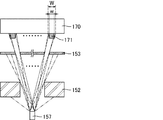
- 15 and 16 are schematic cross-sectional views of each member in the scan vapor deposition method (a method in which vapor deposition is performed while moving (scanning) the substrate) studied by the present inventors.
- 15 and 16 show cross sections perpendicular to the scanning direction of the substrate.
- a limiting plate 152, a mask 153, and a substrate 170 are arranged in this order on a nozzle 157 of a vapor deposition source.
- the substrate 170 is disposed apart from the mask 153.
- the outline of the thin film pattern 171 formed on the substrate 170 is blurred, and the actual width W becomes larger than the designed width w.
- portions where the film thickness gradually decreases hereinafter also referred to as a blurred portion
- the present inventors have found that when the film forming rate is increased, the width of the blurred portion (hereinafter also referred to as the blurred width) is increased as shown in FIG.
- the cause of this is that when the film forming rate is increased, the density of the vapor deposition particles is increased in the vicinity of the nozzle 157 from which the vapor deposition flow is ejected, and the mean free path of the vapor deposition particles is locally shortened, as shown by the broken line in FIG. This is considered to be because the nozzle 157 is virtually increased.
- the blur width increases, it becomes difficult to manufacture a high-definition panel and a high-performance panel.
- the present invention has been made in view of the above situation, and an object of the present invention is to provide an organic EL element manufacturing method and an organic EL display device capable of shortening a film formation time while suppressing an increase in blur width. To do.
- One embodiment of the present invention may be a method for manufacturing an organic electroluminescence element, wherein the manufacturing method is performed with respect to one or more evaporation sources, a limiting plate, and the mask in a state where the substrate is separated from the mask.
- a deposition process may be included in which deposition particles are deposited on the substrate while relatively moving the substrate to form a thin film pattern.
- the one or more deposition sources, the limiting plate, the mask, and the substrate include:
- the restriction plate may be provided with a plurality of openings, and the one or more vapor deposition sources may have a plurality of outlets facing each of the plurality of openings.
- vapor deposition may be performed under the condition of r i ⁇ R i , and the same opening is provided so that the sum of distributions represented by the following formula (1) is 1 or less.
- the plurality of injection ports facing the part are separated from each other. It may be positioned.
- R i represents the maximum deposition rate of the exit port i of the plurality of injection ports facing the same opening, i is 1 or more, represents an integer less than or equal to m, m is the same
- the number of the plurality of injection ports facing the opening is represented, r i represents the actual film formation rate of the injection port i in the vapor deposition step, and n i represents the n value (0 or more) of the injection port i.
- ⁇ i represents an angle formed by a line segment connecting the injection port i and an arbitrary point in the film formation region with the main film formation direction.
- the plurality of injection ports facing the same opening may be arranged along a relative movement direction of the substrate.
- the maximum film formation rate, the actual film formation rate, and the n value of the plurality of injection ports facing the same opening may be equal to each other.
- the maximum film formation rates being equal to each other means that the difference is 0.1 ⁇ / sec or less, and the actual film formation rates being equal to each other is 0.1 ⁇ / sec.
- Means that the n values are equal to each other means that the difference is 0.1 or less.
- At least one of the maximum film formation rate, the actual film formation rate, and the n value may be different from each other.
- the maximum film formation rates differ from each other means that the difference is larger than 0.1 ⁇ / sec, and the actual film formation rates differ from each other from the difference of 0.1 ⁇ / sec.
- the n values are different from each other, which means that the difference is larger than 0.1.
- D is the distance between the two most distant ejection openings
- A is the length of the mask opening in the relative movement direction of the substrate.
- Another aspect of the present invention may be an organic electroluminescence display device including an organic electroluminescence element manufactured by the manufacturing method according to the present invention.
- Still another aspect of the present invention is a vapor deposition apparatus including one or more vapor deposition sources, a limiting plate, and a mask, wherein the vapor deposition apparatus has the substrate separated from the mask, and the one or more vapor deposition sources, Evaporation is performed while moving the substrate relative to the restriction plate and the mask, the one or more vapor deposition sources, the restriction plate, the mask, and the substrate are arranged in this order, A plurality of openings may be provided, and the one or more evaporation sources may be provided with a plurality of outlets facing each of the plurality of openings.
- the manufacturing method of an organic EL element and an organic EL display apparatus which can shorten film-forming time can be implement
- FIG. 2 is a schematic plan view illustrating a configuration in a display region of the organic EL display device illustrated in FIG. 1.
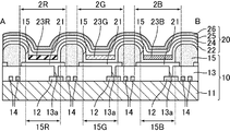
- FIG. 3 is a schematic cross-sectional view showing a configuration of a TFT substrate of the organic EL display device shown in FIG. 1, and corresponds to a cross section taken along line AB in FIG. 3 is a flowchart for explaining a manufacturing process of the organic EL display device according to the first embodiment.
- FIG. 3 is a schematic perspective view of each member in the light emitting layer vapor deposition step of Embodiment 1.
- FIG. 3 is a schematic cross-sectional view of each member in the light emitting layer vapor deposition step of Embodiment 1.
- the film thickness distribution in the X-axis direction of the pattern of the thin film actually formed and the pattern on the setting of the thin film pattern is shown.
- It is a schematic diagram of the injection port and board
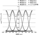
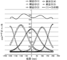
- the expected film thickness distribution of the five injection ports in the scanning direction of the substrate and the sum thereof are shown.
- the expected film thickness distribution of the five injection ports in the scanning direction of the substrate and the sum thereof are shown.
- FIG. 3 is a schematic cross-sectional view of each member in the light emitting layer vapor deposition step of Embodiment 1.
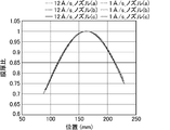
- the film thickness distribution when a thin film is formed at a film formation rate of 1 ⁇ / sec or 12 ⁇ / sec for the three nozzles (a) to (c) is shown. It is the graph which showed the relationship between n value and the maximum film-forming rate. 6 is a graph showing a relationship between a film formation rate and a blur amount in Example 1 and Comparative Example 1. It is a cross-sectional schematic diagram of each member in the scanning vapor deposition method (method of performing vapor deposition while moving (scanning) a substrate) examined by the present inventors. It is a cross-sectional schematic diagram of each member in the scanning vapor deposition method (method of performing vapor deposition while moving (scanning) a substrate) examined by the present inventors.
- Embodiment 1 In the present embodiment, a method for manufacturing a bottom emission type organic EL device for RGB full-color display that extracts light from the TFT substrate side, and an organic EL display device that includes an organic EL device manufactured by the manufacturing method will be mainly described. However, this embodiment is applicable also to the manufacturing method of another type of organic EL element.
- FIG. 1 is a schematic cross-sectional view of an organic EL display device including an organic EL element manufactured by the method for manufacturing an organic EL element of Embodiment 1.
- FIG. 2 is a schematic plan view showing a configuration in the display area of the organic EL display device shown in FIG. 3 is a schematic cross-sectional view showing a configuration of the TFT substrate of the organic EL display device shown in FIG. 1, and corresponds to a cross section taken along line AB in FIG.
- the organic EL display device 1 includes a TFT substrate 10 provided with a TFT 12 (see FIG. 3), and an organic EL element provided on the TFT substrate 10 and connected to the TFT 12. 20, an adhesive layer 30 covering the organic EL element 20, and a sealing substrate 40 disposed on the adhesive layer 30.
- the organic EL element 20 is sealed between the pair of substrates 10 and 40 by bonding the sealing substrate 40 and the TFT substrate 10 on which the organic EL element 20 is laminated using the adhesive layer 30. . This prevents oxygen and moisture from entering the organic EL element 20 from the outside.
- the TFT substrate 10 has a transparent insulating substrate 11 such as a glass substrate as a support substrate.
- a plurality of wirings 14 are formed on the insulating substrate 11, and the plurality of wirings 14 are provided in the horizontal direction and in the vertical direction. And a plurality of signal lines intersecting with each other.
- a gate line driving circuit (not shown) for driving the gate line is connected to the gate line, and a signal line driving circuit (not shown) for driving the signal line is connected to the signal line.
- the organic EL display device 1 is an active matrix display device for RGB full-color display, and each region partitioned by the wiring 14 has red (R), green (G), or blue (B) sub-pixels (dots). ) 2R, 2G or 2B is arranged. The subpixels 2R, 2G, and 2B are arranged in a matrix. Corresponding color organic EL elements 20 and light emitting regions are formed in the sub-pixels 2R, 2G, and 2B of the respective colors.
- the red, green, and blue sub-pixels 2R, 2G, and 2B emit light with red light, green light, and blue light, respectively, and one pixel 2 is configured from the three sub-pixels 2R, 2G, and 2B. Yes.
- the sub-pixels 2R, 2G, and 2B are provided with openings 15R, 15G, and 15B, respectively, and the openings 15R, 15G, and 15B are formed by red, green, and blue light emitting layers 23R, 23G, and 23B, respectively. Covered.
- the light emitting layers 23R, 23G, and 23B are formed in a stripe shape in the vertical direction.
- the pattern of the light emitting layers 23R, 23G, and 23B is formed by vapor deposition for each color.
- the openings 15R, 15G, and 15B will be described later.
- Each subpixel 2R, 2G, 2B is provided with a TFT 12 connected to the first electrode 21 of the organic EL element 20.
- the light emission intensity of each of the sub-pixels 2R, 2G, and 2B is determined by scanning and selection by the wiring 14 and the TFT 12.
- the organic EL display device 1 realizes image display by selectively emitting the organic EL elements 20 of each color with desired luminance using the TFT 12.
- the configuration of the TFT substrate 10 and the organic EL element 20 will be described in detail. First, the TFT substrate 10 will be described.
- the TFT substrate 10 includes a TFT 12 (switching element) and a wiring 14 formed on the insulating substrate 11, an interlayer film (interlayer insulating film, planarizing film) 13 covering them, and an interlayer film 13. And an edge cover 15 which is an insulating layer formed thereon.
- the TFT 12 is provided corresponding to each sub-pixel 2R, 2G, 2B.
- illustration and description of each layer in TFT12 are abbreviate
- the interlayer film 13 is formed on the insulating substrate 11 over the entire region of the insulating substrate 11.
- a first electrode 21 of the organic EL element 20 is formed on the interlayer film 13.
- the interlayer film 13 is provided with a contact hole 13 a for electrically connecting the first electrode 21 to the TFT 12. Thereby, the TFT 12 is electrically connected to the organic EL element 20 through the contact hole 13a.
- the edge cover 15 prevents the first electrode 21 and the second electrode 26 of the organic EL element 20 from being short-circuited due to a thin organic EL layer or electric field concentration at the end of the first electrode 21. Is formed for. Therefore, the edge cover 15 is formed so as to partially cover the end portion of the first electrode 21.
- the edge cover 15 is provided with the above-described openings 15R, 15G, and 15B.
- Each opening 15R, 15G, 15B of the edge cover 15 becomes a light emitting region of the sub-pixels 2R, 2G, 2B.
- the sub-pixels 2R, 2G, and 2B are partitioned by the edge cover 15 having an insulating property.
- the edge cover 15 also functions as an element isolation film.
- the organic EL element 20 is a light emitting element that can emit light with high luminance by low voltage direct current drive, and includes a first electrode 21, an organic EL layer, and a second electrode 26, which are stacked in this order.
- the first electrode 21 is a layer having a function of injecting (supplying) holes into the organic EL layer.
- the first electrode 21 is connected to the TFT 12 through the contact hole 13a as described above.
- a hole injection layer / hole transport layer 22 As an organic EL layer, from the first electrode 21 side, a hole injection layer / hole transport layer 22, light emitting layers 23R, 23G or 23B, the electron transport layer 24, and the electron injection layer 25 are laminated in this order.
- the order of lamination is that when the first electrode 21 is an anode and the second electrode 26 is a cathode, and when the first electrode 21 is a cathode and the second electrode 26 is an anode, the organic layer is organic.
- the stacking order of the EL layers is reversed.
- the hole injection layer is a layer having a function of increasing the efficiency of hole injection into each of the light emitting layers 23R, 23G, and 23B.
- the hole transport layer is a layer having a function of improving the hole transport efficiency to each of the light emitting layers 23R, 23G, and 23B.
- the hole injection layer / hole transport layer 22 is uniformly formed on the entire display region of the TFT substrate 10 so as to cover the first electrode 21 and the edge cover 15.
- the hole injection layer / hole transport layer 22 in which the hole injection layer and the hole transport layer are integrated is provided as the hole injection layer and the hole transport layer.
- a case will be described as an example.
- the present embodiment is not particularly limited to this case.
- the hole injection layer and the hole transport layer may be formed as independent layers.
- the light emitting layers 23R, 23G, and 23B correspond to the sub-pixels 2R, 2G, and 2B so as to cover the openings 15R, 15G, and 15B of the edge cover 15, respectively. Is formed.
- Each of the light emitting layers 23R, 23G, and 23B is a layer having a function of emitting light by recombining holes injected from the first electrode 21 side with electrons injected from the second electrode 26 side. is there.
- Each of the light emitting layers 23R, 23G, and 23B is formed of a material having high light emission efficiency such as a low molecular fluorescent dye or a metal complex.
- the electron transport layer 24 is a layer having a function of increasing the electron transport efficiency from the second electrode 26 to each of the light emitting layers 23R, 23G, and 23B.
- the electron injection layer 25 is a layer having a function of increasing the efficiency of electron injection from the second electrode 26 to each of the light emitting layers 23R, 23G, and 23B.
- the electron transport layer 24 is uniformly formed on the entire display region of the TFT substrate 10 so as to cover the light emitting layers 23R, 23G and 23B and the hole injection / hole transport layer 22.
- the electron injection layer 25 is uniformly formed on the entire display region of the TFT substrate 10 so as to cover the electron transport layer 24.
- the electron transport layer 24 and the electron injection layer 25 may be formed as independent layers as described above, or may be provided integrally with each other. That is, the organic EL display device 1 may include an electron transport layer / electron injection layer instead of the electron transport layer 24 and the electron injection layer 25.
- the second electrode 26 is a layer having a function of injecting electrons into the organic EL layer.
- the second electrode 26 is uniformly formed on the entire display region of the TFT substrate 10 so as to cover the electron injection layer 25.
- the organic layers other than the light emitting layers 23R, 23G, and 23B are not essential layers as the organic EL layer, and can be appropriately formed according to the required characteristics of the organic EL element 20.
- a carrier blocking layer can also be added to the organic EL layer as necessary.
- a hole blocking layer may be added as a carrier blocking layer between the light emitting layers 23R, 23G, and 23B and the electron transport layer 24, thereby preventing holes from reaching the electron transport layer 24. , Luminous efficiency can be improved.
- first electrode / positive Hole injection layer / hole transport layer / electron injection layer / electron injection layer / electron injection layer / electron injection layer / second electrode (2) First electrode / hole transport layer / light emitting layer / electron transport layer / second electrode (3) First electrode / hole transport layer / light emitting layer / Hole blocking layer / electron transport layer / second electrode (4) first electrode / hole transport layer / light emitting layer / hole blocking layer / electron transport layer / electron injection layer / second electrode (5) first electrode / Hole injection layer / hole transport layer / light emitting layer / electron transport layer / electron injection layer / second electrode (6) first electrode / hole injection layer / hole transport layer / light emitting layer / hole blocking layer / electron Transport layer / second electrode (7) first electrode / hole injection layer / hole transport layer / light emitting layer / hole blocking layer / electron transport layer / electron injection layer / second electrode (8) first electrode / positive Hole injection layer / hole transport layer / electron transport layer
- the configuration of the organic EL element 20 is not particularly limited to the layer configurations of the above (1) to (8), and a desired layer configuration can be adopted according to the required characteristics of the organic EL element 20.
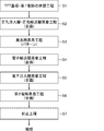
- FIG. 4 is a flowchart for explaining a manufacturing process of the organic EL display device according to the first embodiment.
- the manufacturing method of the organic EL display device includes, for example, a TFT substrate / first electrode manufacturing step S1, a hole injection layer / hole transport layer deposition step S2, and a light emitting layer deposition. It includes a step S3, an electron transport layer vapor deposition step S4, an electron injection layer vapor deposition step S5, a second electrode vapor deposition step S6, and a sealing step S7.
- the stacking order described in the present embodiment is the case where the first electrode 21 is an anode and the second electrode 26 is a cathode, and conversely, the first electrode 21 is a cathode,
- the electrode 26 is used as an anode, the order of stacking the organic EL layers is reversed.
- the materials constituting the first electrode 21 and the second electrode 26 are also reversed.
- a photosensitive resin is applied to the insulating substrate 11 on which the TFTs 12, the wirings 14 and the like are formed by a general method, and the photosensitive resin is patterned by a photolithography technique, thereby insulating the substrate.
- An interlayer film 13 is formed on the substrate 11.
- the thickness is 0.7 to 1.1 mm
- the length in the Y-axis direction is 400 to 500 mm
- the length in the X-axis direction is 300.
- Examples include a glass substrate or a plastic substrate of ⁇ 400 mm.
- a resin such as an acrylic resin or a polyimide resin can be used as a material of the interlayer film 13.
- the acrylic resin include Optomer series manufactured by JSR Corporation.
- a polyimide resin the photo nice series by Toray Industries, Inc. is mentioned, for example.
- the polyimide resin is generally not transparent but colored. Therefore, when a bottom emission type organic EL display device is manufactured as the organic EL display device 1 as shown in FIG. 3, a transparent resin such as an acrylic resin is more preferably used as the interlayer film 13. .
- the film thickness of the interlayer film 13 is not particularly limited as long as the level difference due to the TFT 12 can be compensated. For example, it may be approximately 2 ⁇ m.
- a contact hole 13 a for electrically connecting the first electrode 21 to the TFT 12 is formed in the interlayer film 13.
- a conductive film for example, an ITO (Indium Tin Oxide) film is formed to a thickness of 100 nm by a sputtering method or the like.
- ITO Indium Tin Oxide
- the ITO film is etched using ferric chloride as an etchant. Thereafter, the photoresist is stripped using a resist stripping solution, and substrate cleaning is further performed. As a result, the first electrodes 21 are formed in a matrix on the interlayer film 13.
- Examples of the conductive film material used for the first electrode 21 include transparent conductive materials such as ITO, IZO (Indium Zinc Oxide), and gallium-doped zinc oxide (GZO); gold (Au), nickel Metal materials such as (Ni) and platinum (Pt) can be used.
- transparent conductive materials such as ITO, IZO (Indium Zinc Oxide), and gallium-doped zinc oxide (GZO); gold (Au), nickel Metal materials such as (Ni) and platinum (Pt) can be used.
- a vacuum deposition method As a method for laminating the conductive film, in addition to the sputtering method, a vacuum deposition method, a CVD (Chemical Vapor Deposition) method, a plasma CVD method, a printing method, or the like can be used.
- a vacuum deposition method As a method for laminating the conductive film, in addition to the sputtering method, a vacuum deposition method, a CVD (Chemical Vapor Deposition) method, a plasma CVD method, a printing method, or the like can be used.
- CVD Chemical Vapor Deposition
- the thickness of the 1st electrode 21 is not specifically limited, As above-mentioned, it can be 100 nm, for example.
- the edge cover 15 is formed with a film thickness of, for example, approximately 1 ⁇ m by the same method as the interlayer film 13.
- the same insulating material as that of the interlayer film 13 can be used.
- the TFT substrate 10 and the first electrode 21 are manufactured (S1).
- the TFT substrate 10 that has undergone the above steps is subjected to reduced pressure baking for dehydration and oxygen plasma treatment for cleaning the surface of the first electrode 21.
- the hole injection layer and the hole transport layer are formed on the TFT substrate 10 by using a general vapor deposition apparatus. (S2).
- an open mask having an opening corresponding to the entire surface of the display area is adhered and bonded to the TFT substrate 10 after alignment adjustment. Then, while rotating the TFT substrate 10 and the open mask together, the vapor deposition particles scattered from the vapor deposition source are uniformly vapor deposited on the entire display area through the opening of the open mask.
- vapor deposition on the entire surface of the display region means vapor deposition without interruption between adjacent sub-pixels of different colors.
- Examples of the material for the hole injection layer and the hole transport layer include benzine, styrylamine, triphenylamine, porphyrin, triazole, imidazole, oxadiazole, polyarylalkane, phenylenediamine, arylamine, oxazole, anthracene, and fluorenone. , Hydrazone, stilbene, triphenylene, azatriphenylene, and derivatives thereof; polysilane compounds; vinyl carbazole compounds; thiophene compounds, aniline compounds, etc., heterocyclic conjugated monomers, oligomers, or polymers; etc. Is mentioned.
- the hole injection layer and the hole transport layer may be integrated as described above, or may be formed as independent layers.
- Each film thickness is, for example, 10 to 100 nm.
- the material of the hole injection layer / hole transport layer 22 is, for example, 4,4′-bis [N— ( 1-naphthyl) -N-phenylamino] biphenyl ( ⁇ -NPD) can be used.
- the film thickness of the hole injection layer / hole transport layer 22 can be set to, for example, 30 nm.
- the light emitting layers 23R, 23G, and 23B are formed on the hole injection layer / hole transport layer 22 so as to cover the openings 15R, 15G, and 15B of the edge cover 15 corresponding to the sub-pixels 2R, 2G, and 2B. Each is formed separately (pattern formation) (S3).
- a material having a high light emission efficiency such as a low molecular fluorescent dye or a metal complex is used.
- Examples of the material of the light emitting layers 23R, 23G, and 23B include anthracene, naphthalene, indene, phenanthrene, pyrene, naphthacene, triphenylene, anthracene, perylene, picene, fluoranthene, acephenanthrylene, pentaphen, pentacene, coronene, butadiene, and coumarin.
- each light emitting layer 23R, 23G, 23B is, for example, 10 to 100 nm.
- the manufacturing method according to the present invention can be particularly suitably used for forming such light emitting layers 23R, 23G, and 23B.
- the electron transport layer 24 is covered with the hole injection layer / hole transport layer 22 and the light emitting layers 23R, 23G, and 23B. Vapor deposition is performed on the entire display area of the TFT substrate 10 (S4).
- the electron injection layer 25 is deposited on the entire display region of the TFT substrate 10 so as to cover the electron transport layer 24 by the same method as in the hole injection layer / hole transport layer deposition step S2 (S5). .
- Examples of the material for the electron transport layer 24 and the electron injection layer 25 include quinoline, perylene, phenanthroline, bisstyryl, pyrazine, triazole, oxazole, oxadiazole, fluorenone, and derivatives and metal complexes thereof; LiF (lithium fluoride) );
- Alq3 tris (8-hydroxyquinoline) aluminum
- anthracene naphthalene
- phenanthrene pyrene
- anthracene perylene
- butadiene coumarin
- acridine stilbene
- 1,10-phenanthroline and derivatives thereof Metal complex
- LiF LiF
- the electron transport layer 24 and the electron injection layer 25 may be integrated or formed as independent layers.
- Each film thickness is, for example, 1 to 100 nm, preferably 10 to 100 nm.
- the total film thickness of the electron transport layer 24 and the electron injection layer 25 is, for example, 20 to 200 nm.
- Alq3 is used as the material of the electron transport layer 24, and LiF is used as the material of the electron injection layer 25.
- the thickness of the electron transport layer 24 is 30 nm, and the thickness of the electron injection layer 25 is 1 nm.
- the second electrode 26 is deposited on the entire surface of the display region of the TFT substrate 10 so as to cover the electron injection layer 25 by the same method as in the hole injection layer / hole transport layer deposition step (S2) ( S6).
- the organic EL element 20 including the organic EL layer, the first electrode 21 and the second electrode 26 is formed on the TFT substrate 10.
- Electrode material of the second electrode 26 a metal having a small work function is preferably used.
- examples of such electrode materials include magnesium alloys (MgAg, etc.), aluminum alloys (AlLi, AlCa, AlMg, etc.), metallic calcium, and the like.
- the thickness of the second electrode 26 is, for example, 50 to 100 nm.
- the second electrode 26 is formed from an aluminum thin film having a thickness of 50 nm.
- the TFT substrate 10 on which the organic EL element 20 is formed and the sealing substrate 40 are bonded together using the adhesive layer 30, and the organic EL element 20 is sealed.
- sealing substrate 40 for example, an insulating substrate such as a glass substrate or a plastic substrate having a thickness of 0.4 to 1.1 mm is used.
- the vertical length and the horizontal length of the sealing substrate 40 may be appropriately adjusted according to the size of the target organic EL display device 1, and an insulating substrate having substantially the same size as the insulating substrate 11 of the TFT substrate 10 is used. After sealing the organic EL element 20, it may be divided according to the size of the target organic EL display device 1.
- the sealing method of the organic EL element 20 is not particularly limited to the above-described method, and any other sealing method can be employed.
- Other sealing methods include, for example, a method in which engraved glass is used as the sealing substrate 40 and sealing is performed in a frame shape with a sealing resin, frit glass, or the like, or between the TFT substrate 10 and the sealing substrate 40 For example, a method of filling the resin in between.
- a protective film (not shown) is provided on the second electrode 26 so as to cover the second electrode 26 in order to prevent oxygen and moisture from entering the organic EL element 20 from the outside. It may be.
- the protective film can be formed of an insulating or conductive material. Examples of such a material include silicon nitride and silicon oxide.
- the thickness of the protective film is, for example, 100 to 1000 nm.
- the organic EL display device 1 is completed.
- the organic EL display device 1 when the TFT 12 is turned on by signal input from the wiring 14, holes are injected from the first electrode 21 to the organic EL layer. On the other hand, electrons are injected from the second electrode 26 into the organic EL layer, and holes and electrons are recombined in the light emitting layers 23R, 23G, and 23B.
- the light emitting material is excited by the energy of recombination of holes and electrons, and light is emitted when the excited state returns to the ground state.
- a predetermined image is displayed by controlling the light emission luminance of each of the sub-pixels 2R, 2G, and 2B.
- the light emitting layer deposition step S3 corresponds to the vapor deposition step of the manufacturing method according to the present invention.
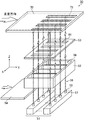
- FIG. 5 is a schematic perspective view of each member in the light emitting layer vapor deposition step of the first embodiment.
- FIG. 6 is a schematic cross-sectional view of each member in the light emitting layer vapor deposition step of the first embodiment.
- FIG. 6 shows a cross section orthogonal to the scanning direction of the substrate, that is, an XZ plane.
- the light emitting layer deposition step S ⁇ b> 3 is performed using a deposition apparatus 50.
- the vapor deposition apparatus 50 includes a vacuum chamber (not shown) and a vacuum pump (not shown) connected to the vacuum chamber.
- a vacuum chamber In the vacuum chamber, a plurality of vapor deposition sources 51, a restriction plate 52 disposed on the vapor deposition source 51, a mask (vapor deposition mask) 53 disposed on the restriction plate 52, a shutter 54, and a substrate (covered)
- a substrate holding mechanism (not shown) for holding a film forming substrate 70, a substrate moving mechanism (not shown) for moving the substrate 70 in the XY plane, that is, in a horizontal direction, and an alignment mechanism (not shown). It has.
- the vapor deposition source 51, the limiting plate 52, and the mask 53 are integrated as one unit.
- the substrate holding mechanism for example, an electrostatic chuck can be used, and the substrate moving mechanism includes, for example, a driving motor.
- the alignment mechanism is for controlling the relative position of the substrate 70 with respect to the unit including the vapor deposition source 51 and the like.
- the alignment mechanism includes a position detection unit such as a CCD camera and a control circuit connected to the position detection unit. Contains.
- the substrate 70 corresponds to the substrate in the manufacturing method according to the present invention.
- the substrate 70 is a substrate manufactured through the TFT substrate / first electrode manufacturing step S1 and the hole injection layer / hole transport layer deposition step S2. As described above, the TFT 12 and the wiring are formed on the insulating substrate 11. 14, the interlayer film 13, the first electrode 21, the edge cover 15, and the hole injection / hole transport layer 22 are formed.
- the vapor deposition sources 51 are arranged m (m is an integer of 2 or more) in the Y-axis direction.
- the vapor deposition source 51 is a container that accommodates the vapor deposition material therein, and has a heating mechanism (not shown) for heating the vapor deposition material.
- k injection ports 55 that are openings are periodically provided in the X-axis direction (k is an integer of 2 or more). Therefore, k injection ports 55 are arranged in the X-axis direction, m in the Y-axis direction, and a total (k ⁇ m).
- the upper limit of k and m is not specifically limited, It can set suitably.
- the vapor deposition material is heated to be vapor by the heating mechanism, and this vapor diffuses in the vapor deposition source 51 and is ejected upward from the injection port 55. As a result, a vapor deposition flow 56 that is a flow of vapor deposition particles is generated from each injection port 55.
- each injection port 55 is not particularly limited and can be set as appropriate.
- a circular shape, an elliptical shape, a rectangular shape, and the like can be mentioned.
- a circular shape is preferable.
- the vapor deposition flow 51 is ejected isotropically from the injection port 55, so that the film thickness distribution of the formed thin film has the same distribution in the scanning direction of the substrate 70 and the direction orthogonal to the direction. Show. Therefore, the design of the vapor deposition apparatus 50 becomes easy.
- each ejection port 55 is an ellipse or a rectangle, and each ejection port 55 is arranged so that the longitudinal direction thereof is along the scanning direction of the substrate 70, the vapor deposition flow 56 adjacent in the scanning direction of the substrate 70. In the meantime, the scattering of the deposited particles may increase.
- the plane shape of each ejection port 55 is an ellipse or a rectangle, and each ejection port 55 is arranged so that its longitudinal direction is perpendicular to the scanning direction of the substrate 70, the pattern of the thin film to be formed Bokeh width tends to increase.
- planar shape of the injection port 55 typically, a rectangle with a width of 4 mm in the X-axis direction and a width of 50 mm in the Y-axis direction, or a circle with a diameter of 2 mm or 4 mm can be given.
- the planar shape of the ejection ports 55 can be set independently of each other, but usually all the ejection ports 55 are set to the same planar shape.
- each injection port 55 is not particularly limited and can be set as appropriate, but is preferably 0.1 mm 2 to 1000 mm 2 . If it is less than 0.1 mm 2 , the injection port 55 may be clogged with the vapor deposition material. On the other hand, if it exceeds 1000 mm 2 , the scattering of the vapor deposition particles becomes large, and the utilization efficiency of the vapor deposition material may be greatly reduced. Since the vapor deposition material for organic EL elements is expensive, if the utilization efficiency of the vapor deposition material is greatly reduced, the productivity is lowered.
- the size (area) of the injection ports 55 can be set independently of each other, but usually all the injection ports 55 are set to the same size.
- Each injection port 55 may be formed at the tip of a nozzle 57 provided on the upper portion of the vapor deposition source 51 as shown in FIGS.
- the limiting plate 52 is a member for removing unnecessary components (vapor deposition particles) from the vapor deposition flow 56 ejected from the injection port 55.
- the restriction plate 52 has k openings 58 formed at substantially the same pitch as the pitch of the injection ports 55 in the X-axis direction. Under the respective openings 58, m injection ports 55 are located, and a plurality of vapor deposition flows 56 rise from the lower side toward the respective openings 58. Part of the vapor deposition particles included in each vapor deposition flow 56 can pass through the corresponding opening 58, and the rest adheres to the wall surface 59 or the bottom surface 60 of the restriction plate 52 and passes through the opening 58. I can't.
- the limiting plate 52 prevents each vapor deposition flow 56 from passing through the adjacent opening 58.
- the limiting plate 52 By providing the limiting plate 52, it is possible to suppress the incident angle of the vapor deposition flow 56 with respect to the substrate 70 from becoming larger than necessary. Therefore, the size of the blur width of the pattern to be formed can be suppressed.
- m that is, a plurality of injection ports 55 are arranged for one opening 58, the film formation rate is higher than that in the case where one injection port is arranged for one opening. Can be bigger.
- the m injection ports 55 facing the same opening 58 are provided on the same straight line parallel to the relative movement direction of the substrate 70, that is, the Y-axis direction.
- a plurality of aperture groups 61 are formed in the mask 53 at substantially the same pitch as the pitch of the openings 58 in the X-axis direction.
- One opening group 61 is provided for each opening 58.
- Each opening group 61 is disposed so as to face the corresponding opening 58 and m injection ports 57 below it.
- Each aperture group 61 includes a plurality of strip-shaped (slit-shaped) apertures 62.
- Each opening 62 is formed in a shape (for example, a rectangular shape) that is long in the Y-axis direction and short in the X-axis direction, and is disposed substantially parallel to the Y-axis direction.
- a part of the vapor deposition flow 56 that has come to the mask 53 passes through the opening 62 and reaches the substrate 70, and the rest is shielded by the mask 53. Therefore, vapor deposition particles are deposited on the substrate 70 in a pattern corresponding to the opening 62 of the mask 53.
- the mask 53 is smaller than the substrate 70, and at least one side of the mask 53 is shorter than the corresponding side of the vapor deposition region of the substrate 70. As a result, the mask 53 can be easily manufactured, and the occurrence of bending due to the weight of the mask 53 itself is suppressed.
- the mask 53 is spaced apart from the substrate 70, that is, separated from the substrate 70, and a predetermined size is provided between the mask 53 and the substrate 70.
- a gap (gap) is provided. This gap is preferably 0.05 mm or more and 5 mm or less. If this gap is too wide, the blur width of the thin film pattern to be formed becomes large, so a value larger than 5 mm is not practical.
- the gap is preferably as small as possible. However, if the gap between the mask 53 and the substrate 70 is too close, the mask is deposited during vapor deposition due to vibration during scanning of the substrate 70, unevenness of the substrate 70, distortion of the mask 53, and the like. 53 and the substrate 70 may come into contact with each other. Therefore, a value smaller than 0.05 mm is not realistic.
- the distance between the mask 53 and the formation surface of each injection port 55 is also maintained at a predetermined size.
- the interval is preferably 50 mm or more and 2000 mm or less. If these distances are too close, the blur width becomes too large, and a value smaller than 50 mm is not practical.
- a shutter 54 for blocking the vapor deposition flow 56 and a limiting plate 52 for limiting (controlling) the flying range of the vapor deposition particles are disposed. It is not realistic in terms of the structure.
- the value is larger than 2000 mm, the distance between the injection port 55 and the mask 53 and the distance between the injection port 55 and the substrate 70 are both too long, and the utilization efficiency of the vapor deposition material is too low. is not.
- vapor deposition is performed three times to sequentially form the three color light emitting layers 23R, 23G, and 23B.
- vapor deposition particles are attached on the substrate 70 while moving (scanning) the substrate 70 relative to a unit including the vapor deposition source 51 and the like, and the striped thin film is formed as the light emitting layer 23R, 23G, or 23B.
- Pattern 71 is formed.
- the substrate 70 is scanned in the Y-axis direction.
- the vapor deposition source 51, the limiting plate 52, and the mask 53 are integrated, their relative positional relationship is always fixed. Note that both the substrate 70 and the unit including the vapor deposition source 51 may be moved, or the substrate 70 may be fixed and the unit may be moved. Further, the film thickness can be appropriately changed by changing the scanning speed and the number of times.
- the pressure in the vacuum chamber during the deposition is set to about 1 ⁇ 10 ⁇ 5 to 1 ⁇ 10 ⁇ 1 Pa.
- the shutter 54 is provided in a state where it can be inserted between the vapor deposition source 51 and the limiting plate 52. By inserting the shutter 54 between them, the opening 58 of the limiting plate 52 is closed. As described above, by appropriately sandwiching the shutter 54 between the vapor deposition source 51 and the limiting plate 52, it is possible to prevent vapor deposition on an extra portion (non-deposition region).
- each injection port 55 From the viewpoint of shortening the film formation time, it is preferable to increase the film formation rate by each injection port 55 and increase the density of the vapor deposition particles in each vapor deposition flow 56, but if it is excessively large, the blur width is increased as described above. The problem of an increase in the number will occur. Therefore, in the present embodiment, from the viewpoint of achieving both shortening the film formation time and preventing the increase in the blur width, the arrangement location of each injection port 55 is determined and the film formation rate of each injection port 55 is controlled. Hereinafter, those methods will be described in detail.
- the n value is calculated for each injection port 55.
- the thickness of a thin film formed by a vacuum deposition method exhibits a distribution according to a so-called cosine n-law. That is, an angle formed by a line segment connecting an injection port (usually the center thereof) and an arbitrary point in a region (film formation region) where a thin film is formed by the vapor deposition flow from the injection port with the main film formation direction. Is ⁇ , the thickness distribution of the thin film to be formed is represented by cos (n + 3) ⁇ .
- n (n value) is a number of 0 or more, and takes a value specific to the injection port.
- the main film forming direction is a direction from the injection port (usually the center) to the point where the film thickness is maximum.
- a vapor deposition flow is individually generated from each injection port 55, and vapor deposition particles are vapor-deposited on separate test substrates (for example, glass substrates) to form a thin film.
- test substrates for example, glass substrates
- each test substrate is fixed, and the mask 53 is not disposed. Therefore, the formed thin film is not patterned.
- the film thickness distribution of each thin film in a certain direction is measured, and the n value of each injection port 55 is calculated by fitting the graph of cos (n + 3) ⁇ while changing n .
- the maximum film formation rate R of each injection port 55 is obtained. Specifically, vapor deposition flows are individually generated from each injection port 55 at a plurality of film formation rates, and vapor deposition particles are vapor-deposited on separate test substrates (for example, glass substrates) via a mask 53. A thin film pattern is formed. In other words, the thin film pattern is formed under the same conditions as in the light emitting layer deposition step S3 except that a thin film pattern is separately formed for each injection port 55 at various film formation rates. Subsequently, in the direction orthogonal to the scanning direction of the substrate 70, that is, in the X-axis direction, the film thickness distribution (cross-sectional shape) of each formed thin film pattern is measured, and the distribution is set to the thin film pattern setting. The blur amount is calculated by comparing with the upper film thickness distribution (cross-sectional shape). Hereinafter, the blur amount calculation method will be described with reference to FIG.
- FIG. 7 shows the film thickness distribution in the X-axis direction between the actually formed thin film pattern and the set pattern.
- the actual film thickness distribution is indicated by a solid line
- the designed film thickness distribution is indicated by a broken line.
- the actual film thickness distribution can be measured with a step gauge.
- a TENCOR P-11 manufactured by KLA-Tencor can be used as the level difference meter.
- Each film thickness distribution is normalized so that the maximum film thickness is 1.
- the designed film thickness distribution is determined by geometric conditions such as the shape of the injection port 55, the shape of the opening of the mask 53, the arrangement relationship of each member, and the like.
- the range in which the film thickness is 3% to 97% with respect to the maximum film thickness (100%) is defined as the blur amount.
- the actual cross-sectional shape is rounder than the set cross-sectional shape, and the blur amount in the actual film thickness distribution is larger than the blur amount in the set film thickness distribution.
- the allowable range is a range where the blur amount in the actual film thickness distribution is 1.3 times or less than the blur amount in the designed film thickness distribution, and the maximum film formation rate is within the allowable range. Rate R.
- the lower limit of the film thickness is defined as 3% because the measurement error increases when the amount is less than 3%.
- the upper limit of the film thickness is defined as 97% in the definition of the blur amount.
- the reason why the allowable range of the blur amount is defined as 1.3 times or less is that when the blur range is exceeded, the invalid area (non-light emitting area) increases in the display area.
- the film formation rate is represented by the thickness of the thin film formed per unit time, and the unit is, for example, ⁇ / second (sec).
- the film formation rate is measured at the point where the film thickness of the formed thin film is maximized.
- the n value and the maximum film formation rate are measured for only one of the injection ports, and the n values of the other injection ports 55 are measured.
- the maximum film forming rate may be used. This is because the n value and the maximum film formation rate are almost the same if the planar shape and size are the same.
- R i represents the maximum film formation rate of the injection port i (i is an integer of 1 or more and m or less) among the m injection ports 55 facing the same opening 58
- r i is The actual film-forming rate of the injection port i in the light emitting layer vapor deposition process S3 is represented. That is, at each injection port 55, the actual film formation rate r is controlled so as not to exceed the maximum film formation rate R. Thereby, the increase in the blur width considered to be caused by the increase in the density of the vapor deposition particles in the vicinity of the injection port 55 as described above can be suppressed.
- the distribution regarding the film thickness distribution of the thin film is calculated for each injection port 55 based on the following formula (1), and the calculated distributions of all the injection ports 55 are summed up.
- the m injection ports 55 facing the same opening 58 are arranged apart from each other, that is, apart from each other so that the obtained sum (formula (2) below) is 1 or less.
- the distribution represented by the above formula (1) is the ratio of the actual film formation rate of each injection port 55 to the maximum film formation rate of each injection port 55 in the film thickness distribution by each injection port 55 based on the cosine n-th law.
- the film thickness distribution of a thin film formed at an actual film formation rate can be considered as an expected distribution.
- the distribution represented by the above formula (1) is also referred to as an expected film thickness distribution.
- the injection port 55 By arranging the injection port 55 in this way, it is possible to prevent the thin film pattern 71 from being formed at a film formation rate exceeding the maximum film formation rate in the entire region where the thin film pattern 71 is formed. . Therefore, even if the vapor deposition flows 56 from different injection ports 55 intersect with each other and the vapor deposition particles included in the vapor deposition flows 56 collide with each other, the influence on the blur width is affected by the pattern of the thin film exceeding the maximum film formation rate. Compared with the case of forming, it can be made smaller. Therefore, it is possible to suppress an increase in the blur width.
- a plurality (m) of outlets 55 are disposed below each opening 58, and vapor deposition is performed under the condition of r i ⁇ R i in the light emitting layer vapor deposition step S3.
- the plurality of (m) injection ports 55 facing the same opening 58 are arranged so as to be separated from each other so that the sum of the distribution represented by the above formula (1) is 1 or less. Therefore, in the light emitting layer vapor deposition step S3, it is possible to shorten the film formation time while suppressing an increase in the blur width.
- m injection ports 55 facing the same opening 58 are arranged along the relative movement direction of the substrate 70, that is, the Y-axis direction. Therefore, the vapor deposition particles fly on the substrate 70 in parallel with the relative movement direction of the substrate 70 from the plurality of injection ports 55. Therefore, compared with the case where only one injection port 55 is arranged for one opening 58 or the case where m number of injection ports 55 facing the same opening 58 are not arranged along the Y-axis direction, the process is completed. The film rate can be effectively increased, and the productivity can be greatly improved.
- the maximum film formation rates of the m injection ports 55 facing the same opening 58 may be equal to each other, and their actual film formation rates may be equal to each other. Their n values may be equal to each other.
- At least one of the maximum film formation rate, the actual film formation rate, and the n value in at least two of the m injection ports 55 facing the same opening 58 is: They may be different from each other.
- the maximum film formation rates are different from each other, but the actual film formation rates are equal to each other.
- N values may be equal to each other.
- the maximum film formation rates are equal to each other, and the n values may be equal to each other.
- n Although the values are different from each other, the maximum film formation rates may be equal to each other, and the actual film formation rates may be equal to each other.
- the maximum film formation rates are different from each other, and the actual film formation rates are different from each other. Although the values are different, the n values may be equal to each other. (5) The maximum film formation rates are different from each other.
- the n values are different from each other, but the actual film formation rates may be equal to each other.
- Actual film formation rates are different from each other, although the values are different from each other, the maximum film formation rates may be equal to each other.
- the maximum film formation rates are different from each other, the actual film formation rates are different from each other, and the n values are different from each other. Also good.
- the maximum film formation rate being equal to each other means that the difference is 0.1 ⁇ / sec or less
- the actual film formation rate being equal to each other is that the difference is 0.1 ⁇ / sec or less.
- the n values are equal to each other means that the difference is 0.1 or less.
- the maximum film formation rate being different means that the difference is larger than 0.1 ⁇ / sec, and the actual film formation rate is different from each other means that the difference is larger than 0.1 ⁇ / sec.
- n values are different from each other means that the difference is larger than 0.1.
- FIG. 8 is a schematic diagram of an injection port and a substrate for calculating the sum of expected film thickness distributions.
- the five injection ports (1) to (5) are arranged in parallel with the scanning direction of the substrate.
- the interval between each injection port and the substrate 70 was set to 250 mm.
- the n value of each injection port was 50.
- the intervals between adjacent injection ports were all 100 mm.
- the ratio (r i / R i ) of the actual film formation rate at each injection port to the maximum film formation rate at each injection port was 0.96.
- FIG. 9 shows the expected film thickness distribution of the five outlets in the scanning direction of the substrate and the sum thereof. As shown in FIG. 9, the sum of the expected film thickness distributions of all the injection ports (1) to (5) was 1 or less, and the maximum value was 0.998.
- FIG. 10 shows the expected film thickness distribution of the five injection ports in the scanning direction of the substrate and the sum thereof. As shown in FIG. 10, the sum of the expected film thickness distributions of all the injection ports (1) to (5) was 1 or less, and the maximum value was 0.896.
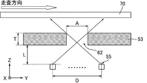
- FIG. 11 is a schematic cross-sectional view of each member in the light emitting layer vapor deposition step of the first embodiment.
- FIG. 11 shows a cross section parallel to the scanning direction of the substrate, that is, a YZ plane.
- the deposition rate is improved by the deposition particles flying from the plurality of injection ports 55 existing below the same opening 58 to the opening 62 of the mask 53. Therefore, from the viewpoint of shortening the film formation time, it is preferable to determine the upper limit value of the interval between the injection ports 55 from the limit arrangement in which these vapor deposition particles can pass through the opening 62 of the mask 53.
- the length of the opening 62 of the mask 53 in the scanning direction of the substrate 70, that is, the Y-axis direction is A
- the thickness of the mask 53 is T
- the distance between each injection port 55 and the mask 53 is the length of the opening 62 of the mask 53 in the scanning direction of the substrate 70, that is, the Y-axis direction.
- Is L and the number of the injection ports 55 arranged below the same opening 58 is J, and the maximum range in which these injection ports 55 can be arranged, that is, between the injection ports 55 at both ends (usually the center).
- D in order to satisfy the above arrangement, D preferably satisfies the relationship of A / T ⁇ D / (T + L) to D ⁇ A ⁇ (T + L) / T.
- the interval d between adjacent injection ports 55 has a relationship of d ⁇ A ⁇ (T + L) / T / (J ⁇ 1). It is preferable to satisfy.
- the interval between adjacent injection ports is approximately It is preferable to set it to 188 mm or less.
- these five injection holes are not arrange
- the lengths of the plurality of openings 62 facing the same opening 58 that is, the plurality of openings 62 included in the same opening group 61, are not uniform in the Y-axis direction, the length of the shortest opening 62 among them is It is preferable to arrange the injection port 55 so as to satisfy the above relational expression, where A is A.
- FIG. 12 shows the film thickness distribution when a thin film is formed at a film formation rate of 1 ⁇ / sec or 12 ⁇ / sec for the three nozzles (a) to (c).
- Alq3 Tris (8-quinolinolato) aluminum
- the shape of each nozzle is a cylindrical shape with an inner diameter of 4 mm and a length of 6 mm
- the planar shape of each injection port is a circle with a diameter of 4 mm. Met.
- the film formation rate when measuring the n value is not particularly limited and can be set as appropriate, but it is usually set to 1.0 ⁇ / sec to 2.0 ⁇ / sec.
- FIG. 13 is a graph showing the relationship between the n value and the maximum film formation rate.
- the interval between the injection port and the substrate was 250 mm, and the interval between the mask and the substrate was 1 mm.
- the maximum film formation rate was determined by the above-described method described with reference to FIG. As shown in FIG. 13 and Table 2 above, it was found that the maximum film formation rate increases as the n value increases, but the maximum film formation rate is gradually saturated.
- the vapor deposition material used for the plurality of vapor deposition sources 51 can be appropriately selected independently. Therefore, these materials may be the same as each other or different from each other. That is, in this embodiment, co-evaporation may be performed.
- the number of the vapor deposition sources 51 is not specifically limited, For example, one may be sufficient. In this case, a plurality of injection ports may be provided in the Y-axis direction for one vapor deposition source.
- the direction of the vapor deposition source 51, the limiting plate 52, the mask 53, and the substrate 70 is not particularly limited as long as they are arranged in this order.
- the vapor deposition source 51, the limiting plate 52, the mask 53, and the substrate 70 may be arranged in this order from the top by inverting the structure described above. Further, the above-described structure may be rotated 90 ° around the Y axis, and the vapor deposition source 51, the limiting plate 52, the mask 53, and the substrate 70 may be arranged side by side.
- the organic EL display device 1 may be a monochrome display device, and each pixel may not be divided into a plurality of sub-pixels. In this case, in light emitting layer vapor deposition process S3, vapor deposition may be performed only once and only one color light emitting layer may be formed.
- a thin film pattern may be formed in the same manner as the light emitting layer vapor deposition step S3.
- the electron transport layer 24 may be formed for each color sub-pixel 2R, 2G, 2B.
- Example 1 In this embodiment, three vapor deposition sources are arranged in the Y-axis direction, that is, the substrate scanning direction, and a plurality of outlets are arranged in each vapor deposition source in parallel with the X-axis direction, that is, perpendicular to the substrate scanning direction. did. Therefore, three injection ports are arranged in the Y-axis direction.
- the planar shape of each injection port was a circle having a diameter of 2 mm, the distance between the substrate and the injection port was 220 mm, and the intervals between adjacent injection ports in the Y-axis direction were all 40 mm.
- each injection port was 250, and the maximum film formation rate of each injection port was 1 kg / sec.
- the actual film formation rate of each injection port was set to 0.95 ⁇ / sec or less, and the film formation rates of all the injection ports were set to the same value.
- the thickness of the mask was 0.1 mm, and a plurality of rectangular (slit) openings were provided in the mask.
- the length of each opening in the Y-axis direction was 0.3 mm, and the length (width) of each opening in the X-axis direction was 0.1 mm.
- the vapor deposition process was performed a plurality of times at a plurality of film formation rates to form a plurality of thin film patterns having a maximum film thickness of 150 nm.
- the sum of the expected film thickness distributions expressed by the above formula (2) is 1 or less, and the maximum value is 0.966. Met.
- the following formula (3) may be used.
- X, Z, and TS represent the position, the interval between adjacent injection ports in the Y-axis direction, and the distance between the substrate and the injection port, respectively.
- Comparative Example 1 In this comparative example, the number of vapor deposition sources was changed to one, and a plurality of film formation rates were performed in the same manner as in Example 1 except that the actual film formation rate at each injection port was 3 ⁇ / sec or less. The vapor deposition process was performed a plurality of times to form a plurality of thin film patterns having a maximum film thickness of 150 nm. In this comparative example, only one injection port is arranged in the Y-axis direction.
- FIG. 14 is a graph showing the relationship between the film formation rate and the amount of blur in Example 1 and Comparative Example 1.
- Table 3 shows the film formation rate and the amount of blur in Example 1 and Comparative Example 1.
- the film formation rate of Example 1 represents the total film formation rate of the three injection ports arranged in the Y-axis direction.
- Example 1 As shown in FIG. 14 and Table 3, in Comparative Example 1, the amount of blur increased when the film formation rate was increased, but in Example 1, the amount of blur did not increase even when the film formation rate was increased. Therefore, according to Example 1, it was possible to form an organic EL element with high accuracy and high productivity.
- Comparative Example 2 In this comparative example, a thin film pattern having a maximum film thickness of 150 nm was formed in the same manner as in Example 1 except that the actual film formation rate at each injection port was set to 1.5 ⁇ / sec. In this comparative example, a single thin film pattern was formed by performing the vapor deposition process only once at the film formation rate. In this comparative example, three injection ports are arranged in the Y-axis direction.
- the sum of the expected film thickness distributions represented by the above formula (2) was larger than 1, and the maximum value was 1.549.
- the blur amount of the formed thin film pattern was 14 ⁇ m, which was larger than 10 ⁇ m in the case of Example 1.
- Organic EL display device 2 Pixel 2R, 2G, 2B: Sub-pixel 10: TFT substrate 11: Insulating substrate 12: TFT 13: Interlayer film 13a: Contact hole 14: Wiring 15: Edge covers 15R, 15G, 15B: Opening 20: Organic EL element 21: First electrode 22: Hole injection layer / hole transport layer (organic layer) 23R, 23G, 23B: Light emitting layer (organic layer) 24: Electron transport layer (organic layer) 25: Electron injection layer (organic layer) 26: second electrode 30: adhesive layer 40: sealing substrate 50: vapor deposition apparatus 51: vapor deposition source 52, 152: restriction plate 53, 153: mask (vapor deposition mask) 54: Shutter 55: Ejection port 56: Deposition flow 57, 157: Nozzle 58: Opening portion 59: Wall surface portion 60: Bottom surface portion 61: Opening group 62: Opening 70, 170: Substrate (film formation substrate) 71, 171: Thin film pattern
Landscapes
- Chemical & Material Sciences (AREA)
- Engineering & Computer Science (AREA)
- Chemical Kinetics & Catalysis (AREA)
- Materials Engineering (AREA)
- Mechanical Engineering (AREA)
- Metallurgy (AREA)
- Organic Chemistry (AREA)
- Manufacturing & Machinery (AREA)
- Physics & Mathematics (AREA)
- Optics & Photonics (AREA)
- Electroluminescent Light Sources (AREA)
- Physical Vapour Deposition (AREA)
Abstract
Priority Applications (4)
| Application Number | Priority Date | Filing Date | Title |
|---|---|---|---|
| JP2015522643A JP6199967B2 (ja) | 2013-06-21 | 2014-05-01 | 有機エレクトロルミネッセンス素子の製造方法 |
| US14/900,541 US9537096B2 (en) | 2013-06-21 | 2014-05-01 | Method for producing organic electroluminescent element, and organic electroluminescent display device |
| KR1020167001318A KR101723348B1 (ko) | 2013-06-21 | 2014-05-01 | 유기 일렉트로 루미네센스 소자의 제조 방법 및 유기 일렉트로 루미네센스 표시 장치 |
| CN201480035328.5A CN105324511B (zh) | 2013-06-21 | 2014-05-01 | 有机电致发光元件的制造方法和有机电致发光显示装置 |
Applications Claiming Priority (2)
| Application Number | Priority Date | Filing Date | Title |
|---|---|---|---|
| JP2013131120 | 2013-06-21 | ||
| JP2013-131120 | 2013-06-21 |
Publications (1)
| Publication Number | Publication Date |
|---|---|
| WO2014203632A1 true WO2014203632A1 (fr) | 2014-12-24 |
Family
ID=52104375
Family Applications (1)
| Application Number | Title | Priority Date | Filing Date |
|---|---|---|---|
| PCT/JP2014/062081 Ceased WO2014203632A1 (fr) | 2013-06-21 | 2014-05-01 | Procédé pour la production d'un élément électroluminescent organique et dispositif d'affichage électroluminescent organique |
Country Status (6)
| Country | Link |
|---|---|
| US (1) | US9537096B2 (fr) |
| JP (1) | JP6199967B2 (fr) |
| KR (1) | KR101723348B1 (fr) |
| CN (1) | CN105324511B (fr) |
| TW (1) | TWI606131B (fr) |
| WO (1) | WO2014203632A1 (fr) |
Families Citing this family (9)
| Publication number | Priority date | Publication date | Assignee | Title |
|---|---|---|---|---|
| CN107305899B (zh) * | 2016-04-22 | 2020-02-11 | 中芯国际集成电路制造(上海)有限公司 | 一种半导体器件及其制备方法和电子装置 |
| CN106019819A (zh) * | 2016-07-22 | 2016-10-12 | 京东方科技集团股份有限公司 | 掩膜板及其制作方法 |
| US20220006051A1 (en) * | 2018-09-27 | 2022-01-06 | Sharp Kabushiki Kaisha | Display device |
| JP6586216B1 (ja) * | 2018-11-22 | 2019-10-02 | 長州産業株式会社 | 蒸着装置及び蒸着方法 |
| CN109536888A (zh) * | 2018-12-28 | 2019-03-29 | 湖畔光电科技(江苏)有限公司 | 一种改进的oled蒸镀装置及其改善蒸镀阴影效应的方法 |
| CN111684100B (zh) * | 2019-01-10 | 2022-09-27 | 株式会社爱发科 | 蒸镀装置 |
| KR102787867B1 (ko) * | 2020-07-03 | 2025-04-01 | 삼성디스플레이 주식회사 | 표시 장치의 제조 장치 및 표시 장치의 제조 방법 |
| CN113174561A (zh) * | 2021-04-26 | 2021-07-27 | 睿馨(珠海)投资发展有限公司 | 一种掩膜导向板、掩膜系统及蒸镀掩膜方法 |
| CN117660888A (zh) * | 2022-08-29 | 2024-03-08 | 京东方科技集团股份有限公司 | 蒸镀掩膜板、蒸镀装置及蒸镀方法 |
Citations (6)
| Publication number | Priority date | Publication date | Assignee | Title |
|---|---|---|---|---|
| JP2000068055A (ja) * | 1998-08-26 | 2000-03-03 | Tdk Corp | 有機el素子用蒸発源、この有機el素子用蒸発源を用いた有機el素子の製造装置および製造方法 |
| JP2004238663A (ja) * | 2003-02-05 | 2004-08-26 | Sony Corp | 蒸着装置 |
| JP2007332458A (ja) * | 2006-05-18 | 2007-12-27 | Sony Corp | 蒸着装置および蒸着源ならびに表示装置の製造方法 |
| WO2012098927A1 (fr) * | 2011-01-18 | 2012-07-26 | シャープ株式会社 | Appareil de dépôt par évaporation sous vide, procédé de dépôt par évaporation sous vide, élément électroluminescent organique et appareil d'affichage électroluminescent organique |
| JP2012167309A (ja) * | 2011-02-10 | 2012-09-06 | Canon Tokki Corp | 蒸着装置並びに蒸着方法 |
| JP2012197467A (ja) * | 2011-03-18 | 2012-10-18 | Canon Tokki Corp | 蒸着装置並びに蒸着方法 |
Family Cites Families (11)
| Publication number | Priority date | Publication date | Assignee | Title |
|---|---|---|---|---|
| US4325986A (en) * | 1979-05-29 | 1982-04-20 | University Of Delaware | Method for continuous deposition by vacuum evaporation |
| US6310281B1 (en) * | 2000-03-16 | 2001-10-30 | Global Solar Energy, Inc. | Thin-film, flexible photovoltaic module |
| SG125069A1 (en) * | 2001-05-17 | 2006-09-29 | Sumitomo Chemical Co | Method and system for manufacturing III-V group compound semiconductor and III-V group compound semiconductor |
| US20040060514A1 (en) * | 2002-01-25 | 2004-04-01 | Applied Materials, Inc. A Delaware Corporation | Gas distribution showerhead |
| JP2004225058A (ja) | 2002-11-29 | 2004-08-12 | Sony Corp | 成膜装置および表示パネルの製造装置とその方法 |
| US20080131587A1 (en) * | 2006-11-30 | 2008-06-05 | Boroson Michael L | Depositing organic material onto an oled substrate |
| JP5046882B2 (ja) | 2007-11-21 | 2012-10-10 | 三菱重工業株式会社 | インライン式成膜装置 |
| JP5620146B2 (ja) * | 2009-05-22 | 2014-11-05 | 三星ディスプレイ株式會社Samsung Display Co.,Ltd. | 薄膜蒸着装置 |
| JP5502092B2 (ja) | 2009-09-15 | 2014-05-28 | シャープ株式会社 | 蒸着方法および蒸着装置 |
| US8894458B2 (en) * | 2010-04-28 | 2014-11-25 | Samsung Display Co., Ltd. | Thin film deposition apparatus, method of manufacturing organic light-emitting display device by using the apparatus, and organic light-emitting display device manufactured by using the method |
| JP5883230B2 (ja) | 2011-03-14 | 2016-03-09 | キヤノントッキ株式会社 | 蒸着装置並びに蒸着方法 |
-
2014
- 2014-05-01 WO PCT/JP2014/062081 patent/WO2014203632A1/fr not_active Ceased
- 2014-05-01 US US14/900,541 patent/US9537096B2/en not_active Expired - Fee Related
- 2014-05-01 CN CN201480035328.5A patent/CN105324511B/zh not_active Expired - Fee Related
- 2014-05-01 KR KR1020167001318A patent/KR101723348B1/ko not_active Expired - Fee Related
- 2014-05-01 JP JP2015522643A patent/JP6199967B2/ja active Active
- 2014-05-13 TW TW103116888A patent/TWI606131B/zh not_active IP Right Cessation
Patent Citations (6)
| Publication number | Priority date | Publication date | Assignee | Title |
|---|---|---|---|---|
| JP2000068055A (ja) * | 1998-08-26 | 2000-03-03 | Tdk Corp | 有機el素子用蒸発源、この有機el素子用蒸発源を用いた有機el素子の製造装置および製造方法 |
| JP2004238663A (ja) * | 2003-02-05 | 2004-08-26 | Sony Corp | 蒸着装置 |
| JP2007332458A (ja) * | 2006-05-18 | 2007-12-27 | Sony Corp | 蒸着装置および蒸着源ならびに表示装置の製造方法 |
| WO2012098927A1 (fr) * | 2011-01-18 | 2012-07-26 | シャープ株式会社 | Appareil de dépôt par évaporation sous vide, procédé de dépôt par évaporation sous vide, élément électroluminescent organique et appareil d'affichage électroluminescent organique |
| JP2012167309A (ja) * | 2011-02-10 | 2012-09-06 | Canon Tokki Corp | 蒸着装置並びに蒸着方法 |
| JP2012197467A (ja) * | 2011-03-18 | 2012-10-18 | Canon Tokki Corp | 蒸着装置並びに蒸着方法 |
Also Published As
| Publication number | Publication date |
|---|---|
| US20160149134A1 (en) | 2016-05-26 |
| CN105324511A (zh) | 2016-02-10 |
| KR20160021275A (ko) | 2016-02-24 |
| KR101723348B1 (ko) | 2017-04-05 |
| TWI606131B (zh) | 2017-11-21 |
| CN105324511B (zh) | 2017-09-05 |
| JPWO2014203632A1 (ja) | 2017-02-23 |
| US9537096B2 (en) | 2017-01-03 |
| TW201506178A (zh) | 2015-02-16 |
| JP6199967B2 (ja) | 2017-09-20 |
Similar Documents
| Publication | Publication Date | Title |
|---|---|---|
| JP6199967B2 (ja) | 有機エレクトロルミネッセンス素子の製造方法 | |
| JP5350547B2 (ja) | 被成膜基板および有機el表示装置 | |
| JP5766239B2 (ja) | 蒸着装置及び蒸着方法 | |
| JP5259886B2 (ja) | 蒸着方法及び蒸着装置 | |
| JP5269256B2 (ja) | 蒸着方法及び蒸着装置 | |
| JP5384755B2 (ja) | 被成膜基板、有機el表示装置 | |
| JP6567349B2 (ja) | 蒸着方法及び蒸着装置 | |
| JP5329718B2 (ja) | 蒸着方法、蒸着膜および有機エレクトロルミネッセンス表示装置の製造方法 | |
| JPWO2012099019A1 (ja) | 有機el表示装置および蒸着方法 | |
| WO2015186796A1 (fr) | Procédé d'évaporation et appareil d'évaporation | |
| JP6042988B2 (ja) | 蒸着装置、蒸着方法、及び、有機エレクトロルミネッセンス素子の製造方法 | |
| JP5313406B2 (ja) | 被成膜基板、有機el表示装置 | |
| JP5410618B2 (ja) | 蒸着装置、蒸着方法、並びに、有機エレクトロルミネッセンス表示装置の製造方法 |
Legal Events
| Date | Code | Title | Description |
|---|---|---|---|
| WWE | Wipo information: entry into national phase |
Ref document number: 201480035328.5 Country of ref document: CN |
|
| 121 | Ep: the epo has been informed by wipo that ep was designated in this application |
Ref document number: 14813840 Country of ref document: EP Kind code of ref document: A1 |
|
| ENP | Entry into the national phase |
Ref document number: 2015522643 Country of ref document: JP Kind code of ref document: A |
|
| NENP | Non-entry into the national phase |
Ref country code: DE |
|
| WWE | Wipo information: entry into national phase |
Ref document number: 14900541 Country of ref document: US |
|
| ENP | Entry into the national phase |
Ref document number: 20167001318 Country of ref document: KR Kind code of ref document: A |
|
| 122 | Ep: pct application non-entry in european phase |
Ref document number: 14813840 Country of ref document: EP Kind code of ref document: A1 |