WO2015001792A1 - 双方向dc/dcコンバータ、双方向電力変換器 - Google Patents
双方向dc/dcコンバータ、双方向電力変換器 Download PDFInfo
- Publication number
- WO2015001792A1 WO2015001792A1 PCT/JP2014/003482 JP2014003482W WO2015001792A1 WO 2015001792 A1 WO2015001792 A1 WO 2015001792A1 JP 2014003482 W JP2014003482 W JP 2014003482W WO 2015001792 A1 WO2015001792 A1 WO 2015001792A1
- Authority
- WO
- WIPO (PCT)
- Prior art keywords
- voltage
- switching element
- terminals
- switching
- state
- Prior art date
- Legal status (The legal status is an assumption and is not a legal conclusion. Google has not performed a legal analysis and makes no representation as to the accuracy of the status listed.)
- Ceased
Links
Images


Classifications
-
- H—ELECTRICITY
- H02—GENERATION; CONVERSION OR DISTRIBUTION OF ELECTRIC POWER
- H02M—APPARATUS FOR CONVERSION BETWEEN AC AND AC, BETWEEN AC AND DC, OR BETWEEN DC AND DC, AND FOR USE WITH MAINS OR SIMILAR POWER SUPPLY SYSTEMS; CONVERSION OF DC OR AC INPUT POWER INTO SURGE OUTPUT POWER; CONTROL OR REGULATION THEREOF
- H02M3/00—Conversion of DC power input into DC power output
- H02M3/22—Conversion of DC power input into DC power output with intermediate conversion into AC
- H02M3/24—Conversion of DC power input into DC power output with intermediate conversion into AC by static converters
- H02M3/28—Conversion of DC power input into DC power output with intermediate conversion into AC by static converters using discharge tubes with control electrode or semiconductor devices with control electrode to produce the intermediate AC
- H02M3/325—Conversion of DC power input into DC power output with intermediate conversion into AC by static converters using discharge tubes with control electrode or semiconductor devices with control electrode to produce the intermediate AC using devices of a triode or a transistor type requiring continuous application of a control signal
- H02M3/335—Conversion of DC power input into DC power output with intermediate conversion into AC by static converters using discharge tubes with control electrode or semiconductor devices with control electrode to produce the intermediate AC using devices of a triode or a transistor type requiring continuous application of a control signal using semiconductor devices only
- H02M3/33538—Conversion of DC power input into DC power output with intermediate conversion into AC by static converters using discharge tubes with control electrode or semiconductor devices with control electrode to produce the intermediate AC using devices of a triode or a transistor type requiring continuous application of a control signal using semiconductor devices only of the forward type
- H02M3/33546—Conversion of DC power input into DC power output with intermediate conversion into AC by static converters using discharge tubes with control electrode or semiconductor devices with control electrode to produce the intermediate AC using devices of a triode or a transistor type requiring continuous application of a control signal using semiconductor devices only of the forward type with automatic control of the output voltage or current
-
- H—ELECTRICITY
- H02—GENERATION; CONVERSION OR DISTRIBUTION OF ELECTRIC POWER
- H02M—APPARATUS FOR CONVERSION BETWEEN AC AND AC, BETWEEN AC AND DC, OR BETWEEN DC AND DC, AND FOR USE WITH MAINS OR SIMILAR POWER SUPPLY SYSTEMS; CONVERSION OF DC OR AC INPUT POWER INTO SURGE OUTPUT POWER; CONTROL OR REGULATION THEREOF
- H02M3/00—Conversion of DC power input into DC power output
- H02M3/22—Conversion of DC power input into DC power output with intermediate conversion into AC
- H02M3/24—Conversion of DC power input into DC power output with intermediate conversion into AC by static converters
- H02M3/28—Conversion of DC power input into DC power output with intermediate conversion into AC by static converters using discharge tubes with control electrode or semiconductor devices with control electrode to produce the intermediate AC
- H02M3/325—Conversion of DC power input into DC power output with intermediate conversion into AC by static converters using discharge tubes with control electrode or semiconductor devices with control electrode to produce the intermediate AC using devices of a triode or a transistor type requiring continuous application of a control signal
- H02M3/335—Conversion of DC power input into DC power output with intermediate conversion into AC by static converters using discharge tubes with control electrode or semiconductor devices with control electrode to produce the intermediate AC using devices of a triode or a transistor type requiring continuous application of a control signal using semiconductor devices only
- H02M3/33569—Conversion of DC power input into DC power output with intermediate conversion into AC by static converters using discharge tubes with control electrode or semiconductor devices with control electrode to produce the intermediate AC using devices of a triode or a transistor type requiring continuous application of a control signal using semiconductor devices only having several active switching elements
- H02M3/33576—Conversion of DC power input into DC power output with intermediate conversion into AC by static converters using discharge tubes with control electrode or semiconductor devices with control electrode to produce the intermediate AC using devices of a triode or a transistor type requiring continuous application of a control signal using semiconductor devices only having several active switching elements having at least one active switching element at the secondary side of an isolation transformer
- H02M3/33584—Bidirectional converters
-
- H—ELECTRICITY
- H02—GENERATION; CONVERSION OR DISTRIBUTION OF ELECTRIC POWER
- H02M—APPARATUS FOR CONVERSION BETWEEN AC AND AC, BETWEEN AC AND DC, OR BETWEEN DC AND DC, AND FOR USE WITH MAINS OR SIMILAR POWER SUPPLY SYSTEMS; CONVERSION OF DC OR AC INPUT POWER INTO SURGE OUTPUT POWER; CONTROL OR REGULATION THEREOF
- H02M7/00—Conversion of AC power input into DC power output; Conversion of DC power input into AC power output
- H02M7/66—Conversion of AC power input into DC power output; Conversion of DC power input into AC power output with possibility of reversal
- H02M7/68—Conversion of AC power input into DC power output; Conversion of DC power input into AC power output with possibility of reversal by static converters
- H02M7/72—Conversion of AC power input into DC power output; Conversion of DC power input into AC power output with possibility of reversal by static converters using discharge tubes with control electrode or semiconductor devices with control electrode
- H02M7/79—Conversion of AC power input into DC power output; Conversion of DC power input into AC power output with possibility of reversal by static converters using discharge tubes with control electrode or semiconductor devices with control electrode using devices of a triode or transistor type requiring continuous application of a control signal
- H02M7/797—Conversion of AC power input into DC power output; Conversion of DC power input into AC power output with possibility of reversal by static converters using discharge tubes with control electrode or semiconductor devices with control electrode using devices of a triode or transistor type requiring continuous application of a control signal using semiconductor devices only
-
- H—ELECTRICITY
- H02—GENERATION; CONVERSION OR DISTRIBUTION OF ELECTRIC POWER
- H02M—APPARATUS FOR CONVERSION BETWEEN AC AND AC, BETWEEN AC AND DC, OR BETWEEN DC AND DC, AND FOR USE WITH MAINS OR SIMILAR POWER SUPPLY SYSTEMS; CONVERSION OF DC OR AC INPUT POWER INTO SURGE OUTPUT POWER; CONTROL OR REGULATION THEREOF
- H02M7/00—Conversion of AC power input into DC power output; Conversion of DC power input into AC power output
- H02M7/42—Conversion of DC power input into AC power output without possibility of reversal
- H02M7/44—Conversion of DC power input into AC power output without possibility of reversal by static converters
- H02M7/48—Conversion of DC power input into AC power output without possibility of reversal by static converters using discharge tubes with control electrode or semiconductor devices with control electrode
- H02M7/483—Converters with outputs that each can have more than two voltages levels
- H02M7/487—Neutral point clamped inverters
Definitions
- the present invention generally relates to a bidirectional DC / DC converter and a bidirectional power converter, and more specifically, a bidirectional DC / AC that operates in conjunction with a bidirectional DC / AC inverter that is connected to a commercial power system and performs an interconnection operation.
- the present invention relates to a DC converter and a bidirectional power converter including the bidirectional DC / DC converter.
- V2H vehicle-to-home
- a power conditioner is a bidirectional DC / AC inverter (hereinafter referred to as a bidirectional inverter) that is connected to a commercial power system to perform an interconnection operation, and a bidirectional DC / DC converter that is connected to an in-vehicle storage battery of an electric vehicle. It consists of.
- the bidirectional DC / DC converter has a function of converting the battery voltage of the in-vehicle storage battery into a DC voltage required for the input of the bidirectional inverter, and converts the DC voltage output from the bidirectional inverter into a charging voltage of the in-vehicle storage battery. A function is required.
- a conventional bidirectional DC / DC converter includes a first conversion circuit provided with a half-bridge connection switching element, a voltage doubler rectifier circuit, and a second conversion circuit provided with a full-bridge connection switching element.
- the power transfer between the first conversion circuit and the second conversion circuit is performed via a transformer, and is electrically insulated by the transformer (for example, see Japanese Patent Publication No. 2011-120370). ).
- the power conditioner used in the V2H system is connected between the commercial power system and the electric vehicle, and manages charging / discharging between the in-vehicle storage battery and the commercial power system.
- the power conditioner is generally composed of a bidirectional inverter that is connected to a commercial power system and performs an interconnection operation, and a bidirectional DC / DC converter that is connected to an in-vehicle storage battery of an electric vehicle.
- the bidirectional DC / DC converter needs to have a function to convert power to DC voltage required for input of the bidirectional inverter when discharging the on-board storage battery by connecting to the on-board storage battery of various battery voltages (DC150-450V). become.
- DC150-450V battery voltages
- the voltage of the commercial power system to which the bidirectional inverter is connected is AC200V or AC100V. Therefore, the bidirectional DC / DC converter also needs a function of converting the DC voltage output from the bidirectional inverter connected to the AC200V or AC100V commercial power system into the charging voltage of the in-vehicle storage battery when charging the in-vehicle storage battery. Become.
- the bidirectional DC / DC converter is required to have a wide range of input voltage and output voltage in order to support in-vehicle storage batteries with various battery voltages and commercial power systems with various system voltages. That is, the bidirectional DC / DC converter is required to have a function of boosting and lowering in both directions corresponding to a wide battery voltage range of the in-vehicle storage battery and a wide voltage range of the commercial power system.
- the present invention has been made in view of the above-mentioned reasons, and its object is to provide a bidirectional DC / DC converter capable of bidirectionally boosting and stepping down in response to the wide range of input voltage and output voltage, and bidirectional power. It is to provide a converter.
- the bidirectional DC / DC converter according to the present invention includes a first operation for outputting a second DC voltage obtained by DC / DC conversion of the first DC voltage between the first terminals between the second terminals, A bidirectional DC / DC converter that performs bidirectional voltage conversion by switching between a second operation in which a fourth DC voltage obtained by DC / DC conversion of a third DC voltage between terminals is output between the first terminals.
- a first switching circuit formed of a series circuit, and connected between a connection point of the first switching element and the second switching element and a connection point of the third switching element and the fourth switching element;
- the second winding of the transformer connected between the first to eighth switching elements, the first to eighth rectifying elements connected in reverse parallel to the first to eighth switching elements, and the first terminal.
- a full-wave rectification operation in which a full-wave rectified voltage obtained by full-wave rectifying the voltage of two windings is applied to a series circuit of the third capacitor and the fourth capacitor, and the second short circuit is maintained in a conductive state. And the voltage of the second winding Both-wave voltage doubler rectification operation applied to each of the third capacitor and the fourth capacitor is performed using the first DC voltage between the first terminals and the second DC voltage between the second terminals. And the full-wave rectified voltage obtained by full-wave rectifying the voltage of the first winding while maintaining the first short circuit in a cut-off state during the second operation.
- the double voltage rectification operation applied to each of the second capacitors is based on the magnitude relationship between the fourth DC voltage between the first terminals and the third DC voltage between the second terminals. It is characterized by switching.
- the bidirectional power converter according to the present invention includes a first operation for outputting a second DC voltage obtained by DC / DC conversion of the first DC voltage between the first terminals between the second terminals, and the second terminal.
- the bi-directional DC / DC of the present invention performs bi-directional voltage conversion by switching between the second operation of outputting the fourth direct-current voltage obtained by DC / DC conversion of the third direct-current voltage between the first terminals.
- the converter converts the second DC voltage between the second terminals during the first operation into an AC voltage and outputs the AC voltage, and converts the AC voltage into the third DC voltage during the second operation.
- a bidirectional inverter applied between the second terminals.
- FIG. 2 shows a block configuration of a bidirectional power converter (power conditioner).
- the bidirectional power converter includes a bidirectional DC / DC converter 1, a bidirectional inverter 2, and a capacitor 3.
- an in-vehicle storage battery 4 of an electric vehicle is connected between terminals T11 and T12 (between the first terminals), and a capacitor 3 is connected between terminals T21 and T22 (between the second terminals).
- a capacitor 3 is connected between terminals T31 and T32, and a commercial power system to which commercial power is supplied from a commercial power source 5 is connected between terminals T41 and T42.
- the bidirectional DC / DC converter 1 converts the battery voltage of the in-vehicle storage battery 4 input to the terminals T11 and T12 into an arbitrary DC voltage to convert the terminals T21 and T22. Output from.
- the DC voltage output from the terminals T21 and T22 is smoothed by the capacitor 3 and applied to the terminals T31 and T32 of the bidirectional inverter 2.
- the bidirectional inverter 2 converts the DC voltage input to the terminals T31 and T32 into an AC voltage linked to the commercial power system and outputs the AC voltage from the terminals T41 and T42.
- the bidirectional inverter 2 converts the commercial voltage (AC voltage) input to the terminals T41 and T42 into a DC voltage and outputs the DC voltage from the terminals T31 and T32.
- the DC voltage output from the terminals T31 and T32 is smoothed by the capacitor 3 and applied to the terminals T21 and T22 of the bidirectional DC / DC converter 1.
- the bidirectional DC / DC converter 1 converts the DC voltage input to the terminals T21 and T22 into a charging voltage and outputs the charging voltage from the terminals T11 and T12 to charge the in-vehicle storage battery 4.
- FIG. 1 shows a circuit configuration of the bidirectional DC / DC converter 1.
- the bidirectional DC / DC converter 1 includes switching circuits 11 and 12, a transformer Tr1, diodes D1 to D8, capacitors C1 to C4, short-circuit circuits 13 and 14, and a control unit 15 as main components.
- the switching circuit 11 includes a parallel circuit of switching elements Q1 and Q2 connected in series and switching elements Q3 and Q4 connected in series, and the parallel circuit is connected between terminals T11 and T12. .
- Switching elements Q1, Q4 are located at the diagonal of the full bridge, and switching elements Q2, Q3 are located at the diagonal of the full bridge.
- the switching elements Q1 to Q4 are composed of MOSFET (Metal-Oxide-Semiconductor-Field-Effect-Transistor) elements.
- the switching elements Q1 to Q4 may be composed of an IGBT (Insulated Gate Bipolar Transistor) element or the like in addition to a MOSFET element.
- the switching elements Q1 to Q4 correspond to the first to fourth switching elements of the present invention on a one-to-one basis.
- Diodes D1 to D4 (first to fourth rectifier elements) are connected in reverse parallel to the switching elements Q1 to Q4 in a one-to-one relationship.
- the first winding N1 of the transformer Tr1 is connected between the connection point of the switching elements Q1, Q2 and the connection point of the switching elements Q3, Q4.
- capacitors C1 and C2 (first and second capacitors) is connected between the terminals T11 and T12. Capacitors C1 and C2 have the same capacity.
- the short circuit 13 (first short circuit) is provided between the connection point of the switching elements Q3 and Q4 and the connection point of the capacitors C1 and C2, and conducts and blocks between the connection points.
- the short circuit 13 includes a series circuit of switching elements Q11 and Q12 connected between the connection point of the switching elements Q3 and Q4 and the connection point of the capacitors C1 and C2, and a reverse parallel one-to-one with the switching elements Q11 and Q12. It is composed of connected diodes D11 and D12.
- Switching elements Q11 and Q12 are constituted by MOSFET elements, IGBT elements, or the like.
- the switching circuit 12 (second switching circuit) includes a parallel circuit of switching elements Q5 and Q6 connected in series and switching elements Q7 and Q8 connected in series, and this parallel circuit is connected between terminals T21 and T22.
- Switching elements Q5 and Q8 are located at the diagonal of the full bridge, and switching elements Q6 and Q7 are located at the diagonal of the full bridge.
- Switching elements Q5 to Q8 are composed of elements such as MOSFETs and IGBT elements.
- the switching elements Q5 to Q8 correspond to the fifth to eighth switching elements of the present invention on a one-to-one basis.
- Diodes D5 to D8 are connected in reverse parallel to the switching elements Q5 to Q8 in a one-to-one relationship.
- a series circuit of the second winding N2 of the transformer Tr1 and the inductor L1 is connected between the connection point of the switching elements Q5 and Q6 and the connection point of the switching elements Q7 and Q8.
- a series circuit of capacitors C3 and C4 (third and fourth capacitors) is connected between terminals T21 and T22.
- Capacitors C3 and C4 have the same capacity.
- the short circuit 14 (second short circuit) is provided between the connection point of the switching elements Q7 and Q8 and the connection point of the capacitors C3 and C4, and conducts and blocks between the connection points.
- the short circuit 14 includes a series circuit of switching elements Q13 and Q14 connected between the connection point of the switching elements Q7 and Q8 and the connection point of the capacitors C3 and C4, and a one-to-one antiparallel connection to the switching elements Q13 and Q14. It is composed of connected diodes D13 and D14.
- Switching elements Q13 and Q14 are constituted by MOSFET elements, IGBT elements, or the like.
- the control unit 15 controls the on / off driving of the switching elements Q1 to Q8 based on the voltage V1 between the terminals T11 and T12, the voltage V2 between the terminals T21 and T22, and the charging / discharging current of the in-vehicle storage battery 4.
- the switching operation of the switching circuits 11 and 12 is controlled. Further, the control unit 15 controls the on / off operation of the short-circuit circuits 13 and 14 by controlling the on / off driving of the switching elements Q11 to Q14.
- a control line between the control unit 15 and the switching elements Q1 to Q8 and Q11 to Q14, a detection unit for the voltages V1 and V2, and a detection unit for the charge / discharge current of the in-vehicle storage battery 4 are omitted.
- control unit 15 switches all conduction / cutoff by the short-circuit circuits 13 and 14 based on the magnitude relationship between the DC voltage between the terminals T11 and T12 and the DC voltage between the terminals T21 and T22. Switching between wave rectification operation and double wave voltage rectification.
- the voltage that the bidirectional inverter 2 outputs from the terminals T31 and T32 is DC320V.
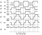
- the control unit 15 When charging the in-vehicle storage battery 4 having a charging voltage of DC 150 V, the control unit 15 performs switching control of the switching elements Q5 to Q8 as shown in FIGS. 3A to 3D to perform a full bridge operation. During the full bridge operation of the switching circuit 12, the control unit 15 maintains the switching elements Q13 and Q14 in the off state.
- Switching elements Q5 and Q6 have an on-duty of about 50%, and the on / off states are opposite to each other. That is, when the switching element Q5 is in the on state, the switching element Q6 is in the off state, and when the switching element Q5 is in the off state, the switching element Q6 is in the on state. Further, a dead time is provided during which the switching elements Q5 and Q6 are simultaneously turned off when the states of the switching elements Q5 and Q6 are reversed (not shown in FIGS. 3A and 3B).
- Switching elements Q7 and Q8 have an on-duty of about 50%, and the on / off states are opposite to each other. That is, when the switching element Q7 is in the on state, the switching element Q8 is in the off state, and when the switching element Q7 is in the off state, the switching element Q8 is in the on state. Further, when the switching elements Q7 and Q8 are inverted, there is a dead time during which the switching elements Q7 and Q8 are simultaneously turned off (not shown in FIGS. 3C and 3D).
- FIG. 3E shows the waveform of the voltage Vn2 of the second winding N2 of the transformer Tr1
- FIG. 3F shows the waveform of the voltage Vn1 of the first winding N1 of the transformer Tr1.
- Vn1 ⁇ 240 V is generated in the first winding N1 of the transformer Tr1, which is stepped down according to the turn ratio of the transformer Tr1. That is, a substantially trapezoidal voltage having a peak voltage of 240V and a substantially trapezoidal voltage having a peak voltage of ⁇ 240V are alternately generated in the first winding N1.
- the control unit 15 maintains the switching elements Q1 to Q4 and the switching elements Q11 and Q12 in the off state, and the voltage Vn1 is full-wave rectified by the diodes D1 to D4.
- the full-wave rectified voltage by the diodes D1 to D4 is applied across the series circuit of the capacitors C1 and C2 and smoothed.
- the voltage across the series circuit of the capacitors C1 and C2 is output as a voltage V1 between the terminals T11 and T12 as shown in FIG. 3G.
- the switching elements Q1 to Q4 may perform full-wave rectification operation by synchronous rectification linked to the on / off operation of the switching elements Q5 to Q8.
- a period in which the switching elements Q5 and Q8 are in the on state and the switching elements Q6 and Q7 are in the off state is defined as T1.
- a period during which the switching elements Q6 and Q7 are on and the switching elements Q5 and Q8 are off is T2.
- These two periods T1 and T2 are energy supply periods from the second winding N2 to the first winding N1.
- a period other than the two periods T1 and T2 is an energy stop period from the second winding N2 to the first winding N1.
- the control unit 15 controls the voltage V1 output from between the terminals T11 and T12 by adjusting the ratio between the energy supply period [T1 + T2] and the energy stop period [T3 + T4]. Specifically, the control unit 15 changes the state inversion phase of the switching elements Q5 and Q6 and the state inversion phase of the switching elements Q7 and Q8 in order to adjust the ratio between the energy supply period and the energy stop period. Perform phase shift operation.
- the terminal T11 ⁇ The voltage V1 output from between T12 is DC240V.
- the phase difference between the ON period of switching element Q5 and the ON period of Q8 is 180 ° and the phase difference between the ON period of switching element Q6 and the ON period of Q7 is 180 °, from between terminals T11 and T12
- the output voltage V1 is approximately 0V.
- the control unit 15 performs on / off control of the switching elements Q5 to Q8 so that the voltage V1 output from between the terminals T11 and T12 becomes DC 150V.
- the control unit 15 When discharging the in-vehicle storage battery 4 having a discharge voltage of DC 150V, the control unit 15 performs switching control of the switching elements Q1 to Q4 as shown in FIGS. 4A to 4D to perform a full bridge operation. During the full bridge operation of the switching circuit 11, the control unit 15 maintains the switching elements Q11 and Q12 in the off state.
- Switching elements Q1 and Q2 have an on-duty of about 50%, and the on / off states are opposite to each other. That is, when the switching element Q1 is in the on state, the switching element Q2 is in the off state, and when the switching element Q1 is in the off state, the switching element Q2 is in the on state. Further, when the switching elements Q1 and Q2 are inverted, a dead time is provided during which the switching elements Q1 and Q2 are simultaneously turned off (not shown in FIGS. 4A and 4B).
- Switching elements Q3 and Q4 have an on-duty of about 50%, and the on / off states are opposite to each other. That is, when the switching element Q3 is in the on state, the switching element Q4 is in the off state, and when the switching element Q3 is in the off state, the switching element Q4 is in the on state.
- a dead time is provided during which the switching elements Q3 and Q4 are simultaneously turned off when the states of the switching elements Q3 and Q4 are reversed (not shown in FIGS. 4C and 4D).
- FIG. 4E shows the waveform of the voltage Vn1 of the first winding N1 of the transformer Tr1
- FIG. 4F shows the waveform of the voltage Vn2 of the second winding N2 of the transformer Tr1.
- the control unit 15 maintains the switching elements Q5 to Q8 in the off state and maintains the switching elements Q13 and Q14 in the on state.
- double voltage rectification is performed in which the voltage of the second winding N2 is applied to each of the capacitors C3 and C4 via the inductor L1 every half cycle, and is smoothed by the capacitors C3 and C4.
- the voltage across the series circuit of the capacitors C3 and C4 is output from the terminals T21 to T22 as the voltage V2 as shown in FIG. 4G.
- a period in which the switching elements Q1, Q4 are in the on state and the switching elements Q2, Q3 are in the off state is defined as T11.
- a period in which the switching elements Q2 and Q3 are on and the switching elements Q1 and Q4 are off is T12.
- These two periods T11 and T12 are energy supply periods from the first winding N1 to the second winding N2.
- the voltage Vn2 is applied to the capacitor C3
- the voltage Vn2 is applied to the capacitor C4.
- a period other than the two periods T11 and T12 is an energy stop period from the first winding N1 to the second winding N2.
- control unit 15 controls the voltage V2 output from between the terminals T21 and T22 by adjusting the ratio between the energy supply period [T11 + T12] and the energy stop period [T13 + T14]. Specifically, the control unit 15 changes the state inversion phase of the switching elements Q1 and Q2 and the state inversion phase of the switching elements Q3 and Q4 in order to adjust the ratio between the energy supply period and the energy stop period. Perform phase shift operation.
- the terminal T21 ⁇ The voltage V2 output from between T22 is DC400V.
- the phase difference between the ON period of the switching element Q1 and the ON period of Q4 is 180 ° and the phase difference between the ON period of the switching element Q2 and the ON period of Q3 is 180 °, from between the terminals T21 and T22
- the output voltage V2 is approximately 0V.
- control unit 15 performs on / off control of the switching elements Q1 to Q4 so that the voltage V2 output from between the terminals T21 and T22 becomes DC320V (capacitor C3: DC160V, capacitor C4: DC160V).
- the control unit 15 When charging the in-vehicle storage battery 4 whose charging voltage is DC450V, the control unit 15 causes the switching elements Q5 to Q8 to perform a full bridge operation (see FIGS. 3A to 3D). During the full bridge operation of the switching circuit 12, the control unit 15 maintains the switching elements Q13 and Q14 in the off state.
- Vn2 320V is applied to the second winding N2 of the transformer Tr1.
- Vn1 240V is generated which is stepped down according to the turn ratio of the transformer Tr1.
- Vn2 ⁇ 320 V is applied to the second winding N2 of the transformer Tr1.
- Vn1 ⁇ 240 V is generated in the first winding N1 of the transformer Tr1, which is stepped down according to the turn ratio of the transformer Tr1. That is, a substantially trapezoidal voltage having a peak voltage of 240V and a substantially trapezoidal voltage having a peak voltage of ⁇ 240V are alternately generated in the first winding N1 (see FIGS. 3E and 3F).
- the control unit 15 maintains the switching elements Q1 to Q4 in the off state and maintains the switching elements Q11 and Q12 in the on state.
- double-wave voltage doubler rectification is performed in which the voltage of the first winding N1 is applied to the capacitors C1 and C2 every half cycle and is smoothed by the capacitors C1 and C2.
- the voltage across the series circuit of the capacitors C1 and C2 is output as a voltage V1 between the terminals T11 and T12.
- the control unit 15 performs on / off control of the switching elements Q5 to Q8 so that the voltage V1 output from between the terminals T11 and T12 becomes DC450V (capacitor C1: DC225V, capacitor C2: DC225V). Specifically, the control unit 15 changes the state inversion phase of the switching elements Q5 and Q6 and the state inversion phase of the switching elements Q7 and Q8 in order to adjust the ratio between the energy supply period and the energy stop period. Perform phase shift operation.
- the control unit 15 When discharging the in-vehicle storage battery 4 whose discharge voltage is DC450V, the control unit 15 causes the switching elements Q1 to Q4 to perform a full bridge operation (see FIGS. 4A to 4D). During the full bridge operation of the switching circuit 11, the control unit 15 maintains the switching elements Q11 and Q12 in the off state.
- Vn2 450V is applied to the first winding N1 of the transformer Tr1.
- Vn2 ⁇ 450 V is applied to the first winding N1 of the transformer Tr1.
- Vn2 ⁇ 600 V, which is boosted according to the turn ratio of the transformer Tr1, is generated. That is, a substantially trapezoidal voltage having a peak voltage of 600V and a substantially trapezoidal voltage having a peak voltage of ⁇ 600V are alternately generated in the second winding N2.
- the control unit 15 maintains the switching elements Q5 to Q8 in the off state and maintains the switching elements Q13 and Q14 in the off state, and the voltage Vn2 is full-wave rectified by the diodes D5 to D8.
- the full-wave rectified voltage by the diodes D5 to D8 is applied across the series circuit of the capacitors C3 and C4 and smoothed.
- the voltage across the series circuit of the capacitors C3 and C4 is output as a voltage V2 from between the terminals T21 and T22.
- the switching elements Q5 to Q8 may perform full-wave rectification operation by synchronous rectification linked to the on / off operation of the switching elements Q1 to Q4.
- the control unit 15 performs on / off control of the switching elements Q1 to Q4 so that the voltage V2 output between the terminals T21 and T22 becomes DC 320V. Specifically, the control unit 15 changes the state inversion phase of the switching elements Q1 and Q2 and the state inversion phase of the switching elements Q3 and Q4 in order to adjust the ratio between the energy supply period and the energy stop period. Perform phase shift operation.
- the control unit 15 switches between the full-wave rectification operation and the double-wave voltage doubler rectification operation based on the magnitude relationship between the DC voltage between the terminals T11 and T12 and the DC voltage between the terminals T21 and T22. Therefore, the bidirectional DC / DC converter 1 can widen the range of the input voltage and the range of the output voltage. it can.
- control unit 15 may switch the full bridge operation and the half bridge operation of the switching circuits 11 and 12 based on the magnitude relationship between the DC voltage between the terminals T11 and T12 and the DC voltage between the terminals T21 and T22. Good.
- the bidirectional DC / DC converter can further widen the input voltage range and the output voltage range.
- the in-vehicle storage battery 4 has a discharge voltage of DC450V
- the control unit 15 When discharging the in-vehicle storage battery 4 having a discharge voltage of DC450V, the control unit 15 maintains the switching elements Q3 and Q4 in the off state and maintains the switching elements Q11 and Q12 in the on state. And the control part 15 controls the on-duty of the switching element Q1 to 50% or less, and controls the on-duty of the switching element Q2 to the same value as the on-duty of the switching element Q1. Furthermore, the control unit 15 performs switching control of the switching elements Q1 and Q2 so that the phase of the on state of the switching element Q1 and the phase of the on state of the switching element Q2 are shifted from each other by 180 degrees. That is, the control unit 15 causes the switching circuit 11 to perform a half bridge operation.
- Vn1 225V (half of 450V) is applied to the first winding N1 of the transformer Tr1.
- Vn2 300 V, which is boosted according to the turns ratio of the transformer Tr1 is generated.
- Vn1 ⁇ 225V is applied to the first winding N1 of the transformer Tr1.
- Vn2 ⁇ 300 V, which is boosted according to the turns ratio of the transformer Tr1, is generated. That is, a substantially trapezoidal voltage having a peak voltage of 300V and a substantially trapezoidal voltage having a peak voltage of ⁇ 300V are alternately generated in the second winding N2.
- the control unit 15 maintains the switching elements Q5 to Q8 in the off state and maintains the switching elements Q13 and Q14 in the on state.
- double voltage rectification is performed in which the voltage of the second winding N2 is applied to each of the capacitors C3 and C4 every half cycle, and is smoothed by the capacitors C3 and C4.
- the voltage across the series circuit of the capacitors C3 and C4 is output as a voltage V1 between the terminals T11 and T12.
- Switching elements Q5 and Q6 may perform synchronous rectification in conjunction with the on / off operation of switching elements Q1 and Q2.
- the bidirectional DC / DC converter 1 described above performs bidirectional voltage conversion by switching between the first operation and the second operation.
- a DC voltage (second DC voltage) obtained by DC / DC conversion of a DC voltage (first DC voltage) between the first terminals (between terminals T11 and T12) is applied between the second terminals (terminal T21). -T22).
- a DC voltage (fourth DC voltage) obtained by DC / DC conversion of a DC voltage (third DC voltage) between the second terminals is output between the first terminals.
- the bidirectional DC / DC converter 1 includes a first switching circuit 11.
- the first switching circuit 11 includes a series circuit of a first switching element Q1 and a second switching element Q2 connected between the first terminals, a third switching element Q3 connected between the first terminals, and This is a circuit composed of a series circuit of the fourth switching element Q4. Further, the bidirectional DC / DC converter 1 is connected between a connection point of the first switching element Q1 and the second switching element Q2 and a connection point of the third switching element Q3 and the fourth switching element Q4. The first winding N1 of the transformer Tr1 is provided. Further, the bidirectional DC / DC converter 1 includes a second switching circuit 12.
- the second switching circuit 12 includes a series circuit of a fifth switching element Q5 and a sixth switching element Q6 connected between the second terminals, a seventh switching element Q7 connected between the second terminals, and This is a circuit composed of a series circuit of eighth switching elements Q8. Further, the bidirectional DC / DC converter 1 is connected between the connection point of the fifth switching element Q5 and the sixth switching element Q6 and the connection point of the seventh switching element Q7 and the eighth switching element Q8. A second winding N2 of the transformer Tr1 is provided. Furthermore, the bidirectional DC / DC converter 1 includes first to eighth rectifier elements D1 to D8 connected in antiparallel to the first to eighth switching elements Q1 to Q8 in a one-to-one manner.
- the bidirectional DC / DC converter 1 includes a series circuit of a first capacitor C1 and a second capacitor C2 connected between the first terminals, and a third capacitor C3 connected between the second terminals. And a series circuit of a fourth capacitor C4. Furthermore, the bidirectional DC / DC converter 1 conducts and cuts off between the connection point of the third switching element Q3 and the fourth switching element Q4 and the connection point of the first capacitor C1 and the second capacitor C2. A first short circuit 13 is provided. Furthermore, the bidirectional DC / DC converter 1 conducts and cuts off between the connection point of the seventh switching element Q7 and the eighth switching element Q8 and the connection point of the third capacitor C3 and the fourth capacitor C4. A second short circuit 14 is provided. Further, the bidirectional DC / DC converter 1 includes a control unit 15 that performs drive control of the first to eighth switching elements Q1 to Q8 and conduction / cutoff control of the first and second short-circuit circuits 13 and 14. .
- the control unit 15 performs the full-wave rectification operation and the double-wave voltage doubler rectification operation during the first operation, with the direct current voltage between the first terminals (first direct current voltage) and the direct current between the second terminals. Switching is performed based on the magnitude relationship with the voltage (second DC voltage).
- the full-wave rectification operation during the first operation the full-wave rectified voltage obtained by full-wave rectifying the voltage of the second winding N2 while maintaining the second short circuit 14 in the cut-off state is converted into the third capacitor C3 and the second 4 is applied to the series circuit of the capacitor C4.
- the second short circuit 14 is maintained in the conductive state, and the voltage of the second winding N2 is applied to each of the third capacitor C3 and the fourth capacitor C4. Apply.
- the control unit 15 performs a full-wave rectification operation and a double-wave voltage doubler rectification operation, a direct current voltage between the first terminals (fourth direct current voltage) and a direct current between the second terminals. Switching is performed based on the magnitude relationship with the voltage (third DC voltage).
- the full-wave rectification operation in the second operation the full-wave rectified voltage obtained by full-wave rectifying the voltage of the first winding N1 while maintaining the first short circuit 13 in the cut-off state is used as the first capacitor C1 and the first capacitor C1.
- the first short circuit 13 is maintained in the conductive state, and the voltage of the first winding N1 is applied to each of the first capacitor C1 and the second capacitor C2.
- the bidirectional DC / DC converter 1 has a DC voltage (first or fourth DC voltage) between the first terminals and a DC voltage (second or third) between the second terminals.
- the full-wave rectification operation and the double-wave voltage doubler rectification operation are switched based on the magnitude relationship with the DC voltage. Therefore, since the bidirectional DC / DC converter can widen the range of the input voltage and the range of the output voltage, the bidirectional DC / DC converter can bidirectionally step up and step down corresponding to the wide range of the input voltage and the output voltage. There is an effect.
- the control unit 15 performs a full-bridge operation and a half-bridge operation by performing a DC voltage between the first terminals (first DC voltage) and a DC voltage between the second terminals ( It is preferable to switch based on the magnitude relationship with the second DC voltage.
- the full bridge operation the first short circuit 13 is maintained in the cut-off state, and switching control is performed as follows.
- the first switching element Q1 and the second switching element Q2 are set so that the on / off state of the first switching element Q1 and the on / off state of the second switching element Q2 are opposite to each other. Switching control.
- the third switching element Q3 and the fourth switching element are switched so that the on / off state of the third switching element Q3 and the on / off state of the fourth switching element Q4 are opposite to each other.
- Switching control is performed on the element Q4.
- the half-bridge operation is performed as follows while maintaining the first short circuit 13 in a conducting state. In the half-bridge operation, the on-duty of the first switching element Q1 is set to 50% or less, and the on-duty of the second switching element Q2 is set to the same value as the on-duty of the first switching element Q1.
- the first switching element Q1 and the second switching element Q2 are set so that the phase difference between the ON state of the first switching element Q1 and the ON state of the second switching element Q2 is 180 degrees. Control switching. In the half-bridge operation, the third switching element Q3 and the fourth switching element Q4 are maintained in the off state.
- the bidirectional DC / DC converter 1 performs a full-bridge operation and a half-bridge operation between the direct current voltage between the first terminals (first direct current voltage) and the second terminal during the first operation. Is switched based on the magnitude relationship with the DC voltage (second DC voltage). Thereby, the bidirectional DC / DC converter 1 can further widen the range of the input voltage and the range of the output voltage.
- the control unit 15 performs a full-bridge operation and a half-bridge operation by performing a DC voltage between the first terminals (fourth DC voltage) and a DC voltage between the second terminals ( It is preferable to switch based on the magnitude relationship with the (third DC voltage).
- the full bridge operation the second short circuit 14 is maintained in the cut-off state, and switching control is performed as follows.
- the fifth switching element Q5 and the sixth switching element Q6 are set so that the on / off state of the fifth switching element Q5 and the on / off state of the sixth switching element Q6 are opposite to each other. Switching control.
- the seventh switching element Q7 and the eighth switching element Q8 are set so that the on / off state of the seventh switching element Q7 and the on / off state of the eighth switching element Q8 are opposite to each other.
- the half-bridge operation operates as follows while maintaining the second short circuit 14 in a conductive state.
- the on-duty of the fifth switching element Q5 is set to 50% or less
- the on-duty of the sixth switching element Q6 is set to the same value as the on-duty of the fifth switching element Q5.
- the fifth switching element Q5 and the sixth switching element Q6 are set so that the phase difference between the on state of the fifth switching element Q5 and the on state of the sixth switching element Q6 becomes 180 degrees.
- the seventh switching element Q7 and the eighth switching element Q8 are maintained in the off state.
- the bidirectional DC / DC converter 1 performs the full-bridge operation and the half-bridge operation between the first terminal and the second terminal during the second operation. Is switched based on the magnitude relationship with the DC voltage (third DC voltage). Thereby, the bidirectional DC / DC converter 1 can further widen the range of the input voltage and the range of the output voltage.
- the bidirectional power converter includes a bidirectional DC / DC converter 1 and a bidirectional inverter 2 according to the present invention.
- the bidirectional DC / DC converter 1 performs bidirectional voltage conversion by switching between the first operation and the second operation.
- a DC voltage (second DC voltage) obtained by DC / DC conversion of a DC voltage (first DC voltage) between the first terminals (between terminals T11 and T12) is applied between the second terminals (terminal T21).
- a DC voltage (fourth DC voltage) obtained by DC / DC conversion of a DC voltage (third DC voltage) between the second terminals is output between the first terminals.
- the bidirectional inverter 2 converts a DC voltage between the second terminals (second DC voltage) into an AC voltage during the first operation and outputs the AC voltage, and converts the AC voltage into a DC voltage (third DC voltage) during the second operation. ) And applied between the second terminals.
- the bidirectional power converter according to the present invention includes a DC voltage (first or fourth DC voltage) between the first terminals and a DC voltage (second or third DC voltage) between the second terminals. )
- a DC voltage first or fourth DC voltage
- a DC voltage second or third DC voltage
Landscapes
- Engineering & Computer Science (AREA)
- Power Engineering (AREA)
- Dc-Dc Converters (AREA)
Abstract
制御部は、車載蓄電池の放電時では、第2の短絡回路を遮断状態に維持して第2巻線の電圧を全波整流する全波整流動作と、第2の短絡回路を導通状態に維持して第2巻線の電圧を両波倍電圧整流する両波倍電圧整流動作とを、第1の端子間の直流電圧と第2の端子間の直流電圧との大小関係に基づいて切り替え、充電時では、第1の短絡回路を遮断状態に維持して第1巻線の電圧を全波整流する全波整流動作と、第1の短絡回路を導通状態に維持して第1巻線の電圧を両波倍電圧整流する両波倍電圧整流動作とを、第1の端子間の直流電圧と第2の端子間の直流電圧との大小関係に基づいて切り替える。
Description
本発明は、一般に双方向DC/DCコンバータおよび双方向電力変換器、より詳細には商用電力系に接続して連系動作を行う双方向DC/ACインバータと連動して動作する双方向DC/DCコンバータ、およびこの双方向DC/DCコンバータを備える双方向電力変換器に関する発明である。
近年、電気自動車(EV)やプラグインハイブリット車(PHEV)などの電動自動車が普及している。そして、電動自動車に搭載した車載蓄電池を家庭用電源として利用するために、V2H(Vehicle to Home)システムに用いるパワーコンディショナ(Power Conditioner)が種々提案されている。
パワーコンディショナは、一般に、商用電力系統に接続して連系動作を行う双方向DC/ACインバータ(以下、双方向インバータという。)と、電動自動車の車載蓄電池に接続した双方向DC/DCコンバータとで構成される。そして、双方向DC/DCコンバータには、車載蓄電池の電池電圧を双方向インバータの入力に必要な直流電圧に電力変換する機能、双方向インバータが出力する直流電圧を車載蓄電池の充電電圧に変換する機能が必要になる。
従来の双方向DC/DCコンバータは、ハーフブリッジ接続のスイッチング素子、倍電圧整流回路を設けた第1の変換回路と、フルブリッジ接続のスイッチング素子を設けた第2の変換回路とを備える。この第1の変換回路と第2の変換回路との間の電力授受はトランスを介して行われており、このトランスによって電気的に絶縁されている(例えば、日本国特許公開番号2011-120370参照)。
V2Hシステムに用いるパワーコンディショナは、商用電力系統と電動自動車との間に接続されて、車載蓄電池と商用電力系統との間の充放電を管理する。パワーコンディショナは、一般に、商用電力系統に接続して連系動作を行う双方向インバータと、電動自動車の車載蓄電池に接続した双方向DC/DCコンバータとで構成される。
そして、双方向DC/DCコンバータには、様々な電池電圧(DC150~450V)の車載蓄電池と接続して、車載蓄電池の放電時に双方向インバータの入力に必要な直流電圧に電力変換する機能が必要になる。双方向インバータの交流出力の仕様がAC200Vである場合、双方向インバータの入力に必要な直流電圧は、DC300~400V程度になる。また、双方向インバータの交流出力の仕様がAC100Vである場合、双方向インバータの入力に必要な直流電圧は、DC150V~200V程度となる。
また、双方向インバータが接続する商用電力系統の電圧は、AC200VまたはAC100Vとなる。したがって、双方向DC/DCコンバータには、車載蓄電池の充電時に、AC200VまたはAC100Vの商用電力系統に接続した双方向インバータが出力する直流電圧を、車載蓄電池の充電電圧に電力変換する機能も必要になる。
したがって、双方向DC/DCコンバータには、様々な電池電圧の車載蓄電池、様々な系統電圧の商用電力系統に対応するために、入力電圧および出力電圧の広範囲化が求められている。すなわち、双方向DC/DCコンバータには、車載蓄電池の広い電池電圧範囲及び商用電力系統の広い電圧範囲に対応して、双方向に昇圧及び降圧する機能が要求されている。
本発明は、上記事由に鑑みてなされており、その目的は、入力電圧および出力電圧の広範囲化に対応して、双方向に昇圧及び降圧することができる双方向DC/DCコンバータ、双方向電力変換器を提供することにある。
本発明の双方向DC/DCコンバータは、第1の端子間の第1直流電圧をDC/DC変換した第2直流電圧を第2の端子間に出力する第1の動作と、前記第2の端子間の第3直流電圧をDC/DC変換した第4直流電圧を前記第1の端子間に出力する第2の動作とを切り換えて、双方向の電圧変換を行う双方向DC/DCコンバータであって、前記第1の端子間に接続された第1のスイッチング素子及び第2のスイッチング素子の直列回路、前記第1の端子間に接続された第3のスイッチング素子及び第4のスイッチング素子の直列回路からなる第1のスイッチング回路と、前記第1のスイッチング素子及び前記第2のスイッチング素子の接続点と前記第3のスイッチング素子及び前記第4のスイッチング素子の接続点との間に接続されたトランスの第1巻線と、前記第2の端子間に接続された第5のスイッチング素子及び第6のスイッチング素子の直列回路、前記第2の端子間に接続された第7のスイッチング素子及び第8のスイッチング素子の直列回路からなる第2のスイッチング回路と、前記第5のスイッチング素子及び前記第6のスイッチング素子の接続点と前記第7のスイッチング素子及び前記第8のスイッチング素子の接続点との間に接続された前記トランスの第2巻線と、前記第1~第8のスイッチング素子に1対1に逆並列接続された第1~第8の整流素子と、前記第1の端子間に接続された第1のコンデンサ及び第2のコンデンサの直列回路と、前記第2の端子間に接続された第3のコンデンサ及び第4のコンデンサの直列回路と、前記第3のスイッチング素子及び前記第4のスイッチング素子の接続点と前記第1のコンデンサ及び前記第2のコンデンサの接続点との間を導通・遮断する第1の短絡回路と、前記第7のスイッチング素子及び前記第8のスイッチング素子の接続点と前記第3のコンデンサ及び前記第4のコンデンサの接続点との間を導通・遮断する第2の短絡回路と、前記第1~第8のスイッチング素子の駆動制御、及び前記第1,第2の短絡回路の導通・遮断制御を行う制御部とを備え、前記制御部は、前記第1の動作時において、前記第2の短絡回路を遮断状態に維持して前記第2巻線の電圧を全波整流した全波整流電圧を、前記第3のコンデンサ及び前記第4のコンデンサの直列回路に印加する全波整流動作と、前記第2の短絡回路を導通状態に維持して、前記第2巻線の電圧を前記第3のコンデンサ及び前記第4のコンデンサのそれぞれに印加する両波倍電圧整流動作とを、前記第1の端子間の前記第1直流電圧と前記第2の端子間の前記第2直流電圧との大小関係に基づいて切り替え、前記第2の動作時において、前記第1の短絡回路を遮断状態に維持して前記第1巻線の電圧を全波整流した全波整流電圧を、前記第1のコンデンサ及び前記第2のコンデンサの直列回路に印加する全波整流動作と、前記第1の短絡回路を導通状態に維持して、前記第1巻線の電圧を前記第1のコンデンサ及び前記第2のコンデンサのそれぞれに印加する両波倍電圧整流動作とを、前記第1の端子間の前記第4直流電圧と前記第2の端子間の前記第3直流電圧との大小関係に基づいて切り替えることを特徴とする。
本発明の双方向電力変換器は、第1の端子間の第1直流電圧をDC/DC変換した第2直流電圧を第2の端子間に出力する第1の動作と、前記第2の端子間の第3直流電圧をDC/DC変換した第4直流電圧を前記第1の端子間に出力する第2の動作とを切り換えて、双方向の電圧変換を行う本発明の双方向DC/DCコンバータと、前記第1の動作時に前記第2の端子間の前記第2直流電圧を交流電圧に変換して出力し、前記第2の動作時に交流電圧を前記第3直流電圧に変換して前記第2の端子間に印加する双方向インバータとを備えることを特徴とする。
以下、本発明の実施の形態を図面に基づいて説明する。
(実施形態)
図2は、双方向電力変換器(パワーコンディショナ)のブロック構成を示す。双方向電力変換器は、双方向DC/DCコンバータ1と、双方向インバータ2と、コンデンサ3とで構成される。
図2は、双方向電力変換器(パワーコンディショナ)のブロック構成を示す。双方向電力変換器は、双方向DC/DCコンバータ1と、双方向インバータ2と、コンデンサ3とで構成される。
双方向DC/DCコンバータ1は、端子T11-T12間(第1の端子間)に、電動自動車の車載蓄電池4を接続し、端子T21-T22間(第2の端子間)に、コンデンサ3を接続している。双方向インバータ2は、端子T31-T32間にコンデンサ3を接続し、端子T41-T42間に商用電源5から商用電力が供給される商用電力系統を接続している。
車載蓄電池4の放電時(第1の動作)において、双方向DC/DCコンバータ1は、端子T11,T12に入力される車載蓄電池4の電池電圧を任意の直流電圧に変換して端子T21,T22から出力する。端子T21,T22から出力された直流電圧はコンデンサ3で平滑されて、双方向インバータ2の端子T31,T32に印加される。そして、双方向インバータ2は、端子T31,T32に入力される直流電圧を、商用電力系統に連系させた交流電圧に変換して端子T41,T42から出力する。
車載蓄電池4の充電時(第2の動作)において、双方向インバータ2は、端子T41,T42に入力される商用電圧(交流電圧)を直流電圧に変換して端子T31,T32から出力する。端子T31,T32から出力された直流電圧はコンデンサ3で平滑されて、双方向DC/DCコンバータ1の端子T21,T22に印加される。そして、双方向DC/DCコンバータ1は、端子T21,T22に入力される直流電圧を充電電圧に変換して端子T11,T12から出力し、車載蓄電池4を充電する。
図1は、双方向DC/DCコンバータ1の回路構成を示す。この双方向DC/DCコンバータ1は、スイッチング回路11,12と、トランスTr1と、ダイオードD1~D8と、コンデンサC1~C4と、短絡回路13,14と、制御部15とを主構成として備える。
スイッチング回路11(第1のスイッチング回路)は、直列接続したスイッチング素子Q1,Q2と直列接続したスイッチング素子Q3,Q4との並列回路を備え、この並列回路が端子T11-T12間に接続されている。スイッチング素子Q1,Q4がフルブリッジの対角に位置し、スイッチング素子Q2,Q3がフルブリッジの対角に位置する。スイッチング素子Q1~Q4は、MOSFET(Metal-Oxide-Semiconductor Field-Effect Transistor)素子で構成される。なお、スイッチング素子Q1~Q4は、MOSFET素子の他、IGBT(Insulated Gate Bipolar Transistor)素子等で構成されてもよい。スイッチング素子Q1~Q4が、本発明の第1~第4のスイッチング素子に1対1に対応している。
スイッチング素子Q1~Q4には、ダイオードD1~D4(第1~第4の整流素子)が1対1に逆並列接続されている。
スイッチング素子Q1,Q2の接続点とスイッチング素子Q3,Q4の接続点との間には、トランスTr1の第1巻線N1が接続されている。
端子T11-T12間には、コンデンサC1,C2(第1,第2のコンデンサ)の直列回路が接続されている。コンデンサC1,C2の容量は、同じである。
短絡回路13(第1の短絡回路)は、スイッチング素子Q3,Q4の接続点とコンデンサC1,C2の接続点との間に設けられて、両接続点間を導通・遮断する。短絡回路13は、スイッチング素子Q3,Q4の接続点とコンデンサC1,C2の接続点との間に接続されたスイッチング素子Q11,Q12の直列回路と、スイッチング素子Q11,Q12に1対1に逆並列接続されたダイオードD11,D12とで構成される。スイッチング素子Q11,Q12は、MOSFET素子、IGBT素子等で構成される。
次に、スイッチング回路12(第2のスイッチング回路)は、直列接続したスイッチング素子Q5,Q6と直列接続したスイッチング素子Q7,Q8との並列回路を備え、この並列回路が端子T21-T22間に接続されている。スイッチング素子Q5,Q8がフルブリッジの対角に位置し、スイッチング素子Q6,Q7がフルブリッジの対角に位置する。スイッチング素子Q5~Q8は、MOSFET、IGBT素子等素子で構成される。スイッチング素子Q5~Q8が、本発明の第5~第8のスイッチング素子に1対1に対応している。
スイッチング素子Q5~Q8には、ダイオードD5~D8(第5~第8の整流素子)が1対1に逆並列接続されている。
スイッチング素子Q5,Q6の接続点とスイッチング素子Q7,Q8の接続点との間には、トランスTr1の第2巻線N2と、インダクタL1との直列回路が接続されている。
端子T21-T22間には、コンデンサC3,C4(第3,第4のコンデンサ)の直列回路が接続されている。コンデンサC3,C4の容量は、同じである。
短絡回路14(第2の短絡回路)は、スイッチング素子Q7,Q8の接続点とコンデンサC3,C4の接続点との間に設けられて、両接続点間を導通・遮断する。短絡回路14は、スイッチング素子Q7,Q8の接続点とコンデンサC3,C4の接続点との間に接続されたスイッチング素子Q13,Q14の直列回路と、スイッチング素子Q13,Q14に1対1に逆並列接続されたダイオードD13,D14とで構成される。スイッチング素子Q13,Q14は、MOSFET素子、IGBT素子等で構成される。
制御部15は、端子T11-T12間の電圧V1、端子T21-T22間の電圧V2、車載蓄電池4の充放電電流に基づいて、スイッチング素子Q1~Q8のオン・オフ駆動を制御することによって、スイッチング回路11,12のスイッチング動作を制御する。さらに、制御部15は、スイッチング素子Q11~Q14のオン・オフ駆動を制御することによって、短絡回路13,14の導通・遮断動作を制御する。なお、図1において、制御部15とスイッチング素子Q1~Q8,Q11~Q14との間の制御線、電圧V1,V2の検出部、車載蓄電池4の充放電電流の検出部は省略している。
本実施形態において、制御部15は、端子T11-T12間の直流電圧と端子T21-T22間の直流電圧との大小関係に基づいて、短絡回路13,14による導通・遮断を切り替えることにより、全波整流動作と両波倍電圧整流とを切り替える。
以下、双方向DC/DCコンバータ1の動作について説明する。
車載蓄電池4の充電電圧および放電電圧(端子T11-T12間の電圧V1)は、車載蓄電池4の仕様や状態に応じて、DC150V~450Vの範囲をとる。また、商用電源5の系統電圧はAC200Vであるので、コンデンサ3の両端電圧はDC320Vとする。また、トランスTr1の巻線N1,N2の巻数比を、N1の巻数:N2の巻数=3:4に設定している。
まず、車載蓄電池4の充電電圧がDC150Vである場合、この車載蓄電池4の充電時の動作について、図3A~図3Gの波形図を用いて説明する。双方向インバータ2が端子T31,T32から出力する電圧はDC320Vである。双方向DC/DCコンバータ1は、端子T21-T22間の電圧V2=DC320V(入力電圧)を、端子T11-T12間の電圧V1=DC150V(出力電圧)に降圧する。
充電電圧がDC150Vである車載蓄電池4の充電時において、制御部15は、スイッチング素子Q5~Q8を、図3A~図3Dに示すようにスイッチング制御して、フルブリッジ動作させる。このスイッチング回路12のフルブリッジ動作時において、制御部15は、スイッチング素子Q13,Q14をオフ状態に維持する。
スイッチング素子Q5,Q6は、オンデューティが約50%で、オン・オフ状態が互いに逆になっている。すなわち、スイッチング素子Q5がオン状態であるとき、スイッチング素子Q6はオフ状態となり、スイッチング素子Q5がオフ状態であるとき、スイッチング素子Q6はオン状態となる。また、スイッチング素子Q5,Q6の状態反転時には、スイッチング素子Q5,Q6が同時にオフ状態となるデッドタイムが設けられている(図3A、図3Bでは図示せず)。
スイッチング素子Q7,Q8は、オンデューティが約50%で、オン・オフ状態が互いに逆になっている。すなわち、スイッチング素子Q7がオン状態であるとき、スイッチング素子Q8はオフ状態となり、スイッチング素子Q7がオフ状態であるとき、スイッチング素子Q8はオン状態となる。また、スイッチング素子Q7,Q8の状態反転時には、スイッチング素子Q7,Q8が同時にオフ状態となるデッドタイムが設けられている(図3C、図3Dでは図示せず)。
図3Eは、トランスTr1の第2巻線N2の電圧Vn2の波形を示し、図3Fは、トランスTr1の第1巻線N1の電圧Vn1の波形を示す。スイッチング素子Q5,Q8が同時にオン状態であり、且つスイッチング素子Q6,Q7が同時にオフ状態であるとき、トランスTr1の第2巻線N2には、Vn2=320Vが印加される。このとき、トランスTr1の第1巻線N1には、トランスTr1の巻数比に応じて降圧されたVn1=240Vが発生する。また、スイッチング素子Q6,Q7が同時にオン状態であり、且つスイッチング素子Q5,Q8が同時にオフ状態であるとき、トランスTr1の第2巻線N2には、Vn2=-320Vが印加される。このとき、トランスTr1の第1巻線N1には、トランスTr1の巻数比に応じて降圧されたVn1=-240Vが発生する。すなわち、第1巻線N1には、ピーク電圧が240Vの略台形状の電圧と、ピーク電圧が-240Vの略台形状の電圧とが、交互に発生する。
そして、制御部15は、スイッチング素子Q1~Q4、スイッチング素子Q11,Q12をオフ状態に維持しており、電圧Vn1はダイオードD1~D4によって全波整流される。ダイオードD1~D4による全波整流電圧は、コンデンサC1,C2の直列回路の両端間に印加されて平滑される。このコンデンサC1,C2の直列回路の両端電圧は、図3Gに示すように電圧V1として端子T11-T12間から出力される。なお、スイッチング素子Q1~Q4は、スイッチング素子Q5~Q8のオン・オフ動作に連動した同期整流によって全波整流動作を行ってもよい。
ここで、スイッチング素子Q5,Q8がオン状態であり、且つスイッチング素子Q6,Q7がオフ状態である期間をT1とする。また、スイッチング素子Q6,Q7がオン状態であり、且つスイッチング素子Q5,Q8がオフ状態である期間をT2とする。この2つの期間T1,T2が、第2巻線N2から第1巻線N1へのエネルギー供給期間となる。2つの期間T1,T2以外の期間(図3中の期間T3,T4)は、第2巻線N2から第1巻線N1へのエネルギー停止期間となる。そして、制御部15は、エネルギー供給期間[T1+T2]とエネルギー停止期間[T3+T4]との比率を調整することによって、端子T11-T12間から出力される電圧V1を制御している。具体的に、制御部15は、エネルギー供給期間とエネルギー停止期間との比率を調整するために、スイッチング素子Q5,Q6の状態反転の位相、及びスイッチング素子Q7,Q8の状態反転の位相を変化させるフェーズシフトの動作を行う。
本実施形態では、スイッチング素子Q5のオン期間とQ8のオン期間との位相差が0°、且つスイッチング素子Q6のオン期間とQ7のオン期間との位相差が0°である場合、端子T11-T12間から出力される電圧V1は、DC240Vとなる。また、スイッチング素子Q5のオン期間とQ8のオン期間との位相差が180°、且つスイッチング素子Q6のオン期間とQ7のオン期間との位相差が180°である場合、端子T11-T12間から出力される電圧V1は、略0Vとなる。そして、制御部15は、端子T11-T12間から出力される電圧V1がDC150Vとなるように、スイッチング素子Q5~Q8をオン・オフ制御する。
次に、車載蓄電池4の放電電圧がDC150Vである場合、この車載蓄電池4の放電時の動作について、図4A~図4Gの波形図を用いて説明する。双方向DC/DCコンバータ1は、端子T11-T12間の電圧V1=DC150V(入力電圧)を、端子T21-T22間の電圧V2=DC320V(出力電圧)に昇圧する。
放電電圧がDC150Vである車載蓄電池4の放電時において、制御部15は、スイッチング素子Q1~Q4を、図4A~図4Dに示すようにスイッチング制御して、フルブリッジ動作させる。このスイッチング回路11のフルブリッジ動作時において、制御部15は、スイッチング素子Q11,Q12をオフ状態に維持する。
スイッチング素子Q1,Q2は、オンデューティが約50%で、オン・オフ状態が互いに逆になっている。すなわち、スイッチング素子Q1がオン状態であるとき、スイッチング素子Q2はオフ状態となり、スイッチング素子Q1がオフ状態であるとき、スイッチング素子Q2はオン状態となる。また、スイッチング素子Q1,Q2の状態反転時には、スイッチング素子Q1,Q2が同時にオフ状態となるデッドタイムが設けられている(図4A、図4Bでは図示せず)。
スイッチング素子Q3,Q4は、オンデューティが約50%で、オン・オフ状態が互いに逆になっている。すなわち、スイッチング素子Q3がオン状態であるとき、スイッチング素子Q4はオフ状態となり、スイッチング素子Q3がオフ状態であるとき、スイッチング素子Q4はオン状態となる。また、スイッチング素子Q3,Q4の状態反転時には、スイッチング素子Q3,Q4が同時にオフ状態となるデッドタイムが設けられている(図4C、図4Dでは図示せず)。
図4Eは、トランスTr1の第1巻線N1の電圧Vn1の波形を示し、図4Fは、トランスTr1の第2巻線N2の電圧Vn2の波形を示す。スイッチング素子Q1,Q4が同時にオン状態であり、且つスイッチング素子Q2,Q3が同時にオフ状態であるとき、トランスTr1の第1巻線N1には、Vn1=150Vが印加される。このとき、トランスTr1の第2巻線N2には、トランスTr1の巻数比に応じて昇圧されたVn2=200Vが発生する。また、スイッチング素子Q2,Q3が同時にオン状態であり、且つスイッチング素子Q1,Q4が同時にオフ状態であるとき、トランスTr1の第1巻線N1には、Vn1=-150Vが印加される。このとき、トランスTr1の第2巻線N2には、トランスTr1の巻数比に応じて昇圧されたVn2=-200Vが発生する。すなわち、第2巻線N2には、ピーク電圧が200Vの略台形状の電圧と、ピーク電圧が-200Vの略台形状の電圧とが、交互に発生する。
そして、制御部15は、スイッチング素子Q5~Q8をオフ状態に維持し、スイッチング素子Q13,Q14をオン状態に維持している。而して、第2巻線N2の電圧がコンデンサC3,C4のそれぞれにインダクタL1を介して半周期毎に印加される両波倍電圧整流が行われ、コンデンサC3,C4によって平滑される。そして、このコンデンサC3,C4の直列回路の両端電圧が、図4Gに示すように電圧V2として端子T21-T22間から出力される。
ここで、スイッチング素子Q1,Q4がオン状態であり、且つスイッチング素子Q2,Q3がオフ状態である期間をT11とする。また、スイッチング素子Q2,Q3がオン状態であり、且つスイッチング素子Q1,Q4がオフ状態である期間をT12とする。この2つの期間T11,T12が、第1巻線N1から第2巻線N2へのエネルギー供給期間となる。期間T11では、コンデンサC3に電圧Vn2が印加され、期間T12では、コンデンサC4に電圧Vn2が印加される。2つの期間T11,T12以外の期間(図4中の期間T13,T14)は、第1巻線N1から第2巻線N2へのエネルギー停止期間となる。そして、制御部15は、エネルギー供給期間[T11+T12]とエネルギー停止期間[T13+T14]との比率を調整することによって、端子T21-T22間から出力される電圧V2を制御している。具体的に、制御部15は、エネルギー供給期間とエネルギー停止期間との比率を調整するために、スイッチング素子Q1,Q2の状態反転の位相、及びスイッチング素子Q3,Q4の状態反転の位相を変化させるフェーズシフトの動作を行う。
本実施形態では、スイッチング素子Q1のオン期間とQ4のオン期間との位相差が0°、且つスイッチング素子Q2のオン期間とQ3のオン期間との位相差が0°である場合、端子T21-T22間から出力される電圧V2は、DC400Vとなる。また、スイッチング素子Q1のオン期間とQ4のオン期間との位相差が180°、且つスイッチング素子Q2のオン期間とQ3のオン期間との位相差が180°である場合、端子T21-T22間から出力される電圧V2は、略0Vとなる。そして、制御部15は、端子T21-T22間から出力される電圧V2がDC320V(コンデンサC3:DC160V、コンデンサC4:DC160V)となるように、スイッチング素子Q1~Q4をオン・オフ制御する。
次に、車載蓄電池4の充電電圧がDC450Vである場合、この車載蓄電池4の充電時の動作について説明する。双方向DC/DCコンバータ1は、端子T21-T22間の電圧V2=DC320V(入力電圧)を、端子T11-T12間の電圧V1=DC450V(出力電圧)に昇圧する。
充電電圧がDC450Vである車載蓄電池4の充電時において、制御部15は、スイッチング素子Q5~Q8をフルブリッジ動作させる(図3A~図3D参照)。このスイッチング回路12のフルブリッジ動作時において、制御部15は、スイッチング素子Q13,Q14をオフ状態に維持する。
スイッチング素子Q5,Q8が同時にオン状態であり、且つスイッチング素子Q6,Q7が同時にオフ状態であるとき、トランスTr1の第2巻線N2には、Vn2=320Vが印加される。このとき、トランスTr1の第1巻線N1には、トランスTr1の巻数比に応じて降圧されたVn1=240Vが発生する。また、スイッチング素子Q6,Q7が同時にオン状態であり、且つスイッチング素子Q5,Q8が同時にオフ状態であるとき、トランスTr1の第2巻線N2には、Vn2=-320Vが印加される。このとき、トランスTr1の第1巻線N1には、トランスTr1の巻数比に応じて降圧されたVn1=-240Vが発生する。すなわち、第1巻線N1には、ピーク電圧が240Vの略台形状の電圧と、ピーク電圧が-240Vの略台形状の電圧とが、交互に発生する(図3E,図3F参照)。
そして、制御部15は、スイッチング素子Q1~Q4をオフ状態に維持し、スイッチング素子Q11,Q12をオン状態に維持している。而して、第1巻線N1の電圧がコンデンサC1,C2のそれぞれに半周期毎に印加される両波倍電圧整流が行われ、コンデンサC1,C2によって平滑される。そして、このコンデンサC1,C2の直列回路の両端電圧が、電圧V1として端子T11-T12間から出力される。
制御部15は、端子T11-T12間から出力される電圧V1がDC450V(コンデンサC1:DC225V、コンデンサC2:DC225V)となるように、スイッチング素子Q5~Q8をオン・オフ制御する。具体的に、制御部15は、エネルギー供給期間とエネルギー停止期間との比率を調整するために、スイッチング素子Q5,Q6の状態反転の位相、及びスイッチング素子Q7,Q8の状態反転の位相を変化させるフェーズシフトの動作を行う。
次に、車載蓄電池4の放電電圧がDC450Vである場合、この車載蓄電池4の放電時の動作について説明する。双方向DC/DCコンバータ1は、端子T11-T12間の電圧V1=DC450V(入力電圧)を、端子T21-T22間の電圧V2=DC320V(出力電圧)に降圧する。
放電電圧がDC450Vである車載蓄電池4の放電時において、制御部15は、スイッチング素子Q1~Q4をフルブリッジ動作させる(図4A~図4D参照)。このスイッチング回路11のフルブリッジ動作時において、制御部15は、スイッチング素子Q11,Q12をオフ状態に維持する。
スイッチング素子Q1,Q4が同時にオン状態であり、且つスイッチング素子Q2,Q3が同時にオフ状態であるとき、トランスTr1の第1巻線N1には、Vn2=450Vが印加される。このとき、トランスTr1の第2巻線N2には、トランスTr1の巻数比に応じて昇圧されたVn1=600Vが発生する。また、スイッチング素子Q2,Q3が同時にオン状態であり、且つスイッチング素子Q1,Q4が同時にオフ状態であるとき、トランスTr1の第1巻線N1には、Vn2=-450Vが印加される。このとき、トランスTr1の第2巻線N2には、トランスTr1の巻数比に応じて昇圧されたVn2=-600Vが発生する。すなわち、第2巻線N2には、ピーク電圧が600Vの略台形状の電圧と、ピーク電圧が-600Vの略台形状の電圧とが、交互に発生する。
そして、制御部15は、スイッチング素子Q5~Q8をオフ状態に維持し、スイッチング素子Q13,Q14をオフ状態に維持しており、電圧Vn2はダイオードD5~D8によって全波整流される。ダイオードD5~D8による全波整流電圧は、コンデンサC3,C4の直列回路の両端間に印加されて平滑される。このコンデンサC3,C4の直列回路の両端電圧は、電圧V2として端子T21-T22間から出力される。なお、スイッチング素子Q5~Q8は、スイッチング素子Q1~Q4のオン・オフ動作に連動した同期整流によって全波整流動作を行ってもよい。
制御部15は、端子T21-T22間から出力される電圧V2がDC320Vとなるように、スイッチング素子Q1~Q4をオン・オフ制御する。具体的に、制御部15は、エネルギー供給期間とエネルギー停止期間との比率を調整するために、スイッチング素子Q1,Q2の状態反転の位相、及びスイッチング素子Q3,Q4の状態反転の位相を変化させるフェーズシフトの動作を行う。
上述のように、制御部15は、端子T11-T12間の直流電圧と端子T21-T22間の直流電圧との大小関係に基づいて、全波整流動作と両波倍電圧整流動作とを切り替える。したがって、双方向DC/DCコンバータ1は、入力電圧の範囲及び出力電圧の範囲を広くすることができるので、入力電圧および出力電圧の広範囲化に対応して、双方向に昇圧及び降圧することができる。
また、制御部15は、端子T11-T12間の直流電圧と端子T21-T22間の直流電圧との大小関係に基づいて、スイッチング回路11,12のフルブリッジ動作とハーフブリッジ動作とを切り替えてもよい。この場合、双方向DC/DCコンバータは、入力電圧の範囲および出力電圧の範囲をさらに広くすることができる。
例えば、車載蓄電池4の放電電圧がDC450Vであり、双方向DC/DCコンバータ1は、端子T11-T12間の電圧V1=DC450V(入力電圧)を、端子T21-T22間の電圧V2=DC320V(出力電圧)に降圧する。
放電電圧がDC450Vである車載蓄電池4の放電時において、制御部15は、スイッチング素子Q3,Q4をオフ状態に維持し、スイッチング素子Q11,Q12をオン状態に維持する。そして、制御部15は、スイッチング素子Q1のオンデューティを50%以下に制御し、スイッチング素子Q2のオンデューティを、スイッチング素子Q1のオンデューティと同じ値に制御する。さらに制御部15は、スイッチング素子Q1のオン状態の位相とスイッチング素子Q2のオン状態の位相とが互いに180度ずれるように、スイッチング素子Q1,Q2をスイッチング制御する。すなわち、制御部15は、スイッチング回路11をハーフブリッジ動作させる。
スイッチング素子Q1がオン状態、且つスイッチング素子Q2がオフ状態であるとき、トランスTr1の第1巻線N1には、Vn1=225V(450Vの半分)が印加される。このとき、トランスTr1の第2巻線N2には、トランスTr1の巻数比に応じて昇圧されたVn2=300Vが発生する。また、スイッチング素子Q2がオン状態、且つスイッチング素子Q1がオフ状態であるとき、トランスTr1の第1巻線N1には、Vn1=-225Vが印加される。このとき、トランスTr1の第2巻線N2には、トランスTr1の巻数比に応じて昇圧されたVn2=-300Vが発生する。すなわち、第2巻線N2には、ピーク電圧が300Vの略台形状の電圧と、ピーク電圧が-300Vの略台形状の電圧とが、交互に発生する。
そして、制御部15は、スイッチング素子Q5~Q8をオフ状態に維持し、スイッチング素子Q13,Q14をオン状態に維持している。而して、第2巻線N2の電圧がコンデンサC3,C4のそれぞれに半周期毎に印加される両波倍電圧整流が行われ、コンデンサC3,C4によって平滑される。そして、このコンデンサC3,C4の直列回路の両端電圧が、電圧V1として端子T11-T12間から出力される。なお、スイッチング素子Q5,Q6は、スイッチング素子Q1,Q2のオン・オフ動作に連動した同期整流を行ってもよい。
制御部15は、端子T21-T22間から出力される電圧V2がDC320V(コンデンサC3:DC160V、コンデンサC4:DC160V)となるように、スイッチング素子Q1,Q2をオン・オフ制御する。具体的に、制御部15は、エネルギー供給期間とエネルギー停止期間との比率を調整するために、スイッチング素子Q1,Q2のオンデューティ制御を行う。
また、車載蓄電池4の充電時においても、制御部15は、端子T11-T12間の直流電圧と端子T21-T22間の直流電圧との大小関係に基づいて、スイッチング回路12のフルブリッジ動作とハーフブリッジ動作とを切り替えてもよい。
なお、上述の各実施形態は本発明の一例である。このため、本発明は、上述の実施形態に限定されることはなく、この実施の形態以外であっても、本発明に係る技術的思想を逸脱しない範囲であれば、設計等に応じて種々の変更が可能であることは勿論である。
(まとめ)
上述の双方向DC/DCコンバータ1は、第1の動作と第2の動作とを切り換えて、双方向の電圧変換を行う。第1の動作は、第1の端子間(端子T11-T12間)の直流電圧(第1直流電圧)をDC/DC変換した直流電圧(第2直流電圧)を第2の端子間(端子T21-T22間)に出力する。第2の動作は、第2の端子間の直流電圧(第3直流電圧)をDC/DC変換した直流電圧(第4直流電圧)を第1の端子間に出力する。双方向DC/DCコンバータ1は、第1のスイッチング回路11を備える。第1のスイッチング回路11は、第1の端子間に接続された第1のスイッチング素子Q1及び第2のスイッチング素子Q2の直列回路、第1の端子間に接続された第3のスイッチング素子Q3及び第4のスイッチング素子Q4の直列回路からなる回路である。さらに、双方向DC/DCコンバータ1は、第1のスイッチング素子Q1及び第2のスイッチング素子Q2の接続点と第3のスイッチング素子Q3及び第4のスイッチング素子Q4の接続点との間に接続されたトランスTr1の第1巻線N1を備える。さらに、双方向DC/DCコンバータ1は、第2のスイッチング回路12を備える。第2のスイッチング回路12は、第2の端子間に接続された第5のスイッチング素子Q5及び第6のスイッチング素子Q6の直列回路、第2の端子間に接続された第7のスイッチング素子Q7及び第8のスイッチング素子Q8の直列回路からなる回路である。さらに、双方向DC/DCコンバータ1は、第5のスイッチング素子Q5及び第6のスイッチング素子Q6の接続点と第7のスイッチング素子Q7及び第8のスイッチング素子Q8の接続点との間に接続されたトランスTr1の第2巻線N2を備える。さらに、双方向DC/DCコンバータ1は、第1~第8のスイッチング素子Q1~Q8に1対1に逆並列接続された第1~第8の整流素子D1~D8を備える。さらに、双方向DC/DCコンバータ1は、第1の端子間に接続された第1のコンデンサC1及び第2のコンデンサC2の直列回路と、第2の端子間に接続された第3のコンデンサC3及び第4のコンデンサC4の直列回路とを備える。さらに、双方向DC/DCコンバータ1は、第3のスイッチング素子Q3及び第4のスイッチング素子Q4の接続点と第1のコンデンサC1及び第2のコンデンサC2の接続点との間を導通・遮断する第1の短絡回路13を備える。さらに、双方向DC/DCコンバータ1は、第7のスイッチング素子Q7及び第8のスイッチング素子Q8の接続点と第3のコンデンサC3及び第4のコンデンサC4の接続点との間を導通・遮断する第2の短絡回路14を備える。さらに、双方向DC/DCコンバータ1は、第1~第8のスイッチング素子Q1~Q8の駆動制御、及び第1,第2の短絡回路13,14の導通・遮断制御を行う制御部15を備える。
上述の双方向DC/DCコンバータ1は、第1の動作と第2の動作とを切り換えて、双方向の電圧変換を行う。第1の動作は、第1の端子間(端子T11-T12間)の直流電圧(第1直流電圧)をDC/DC変換した直流電圧(第2直流電圧)を第2の端子間(端子T21-T22間)に出力する。第2の動作は、第2の端子間の直流電圧(第3直流電圧)をDC/DC変換した直流電圧(第4直流電圧)を第1の端子間に出力する。双方向DC/DCコンバータ1は、第1のスイッチング回路11を備える。第1のスイッチング回路11は、第1の端子間に接続された第1のスイッチング素子Q1及び第2のスイッチング素子Q2の直列回路、第1の端子間に接続された第3のスイッチング素子Q3及び第4のスイッチング素子Q4の直列回路からなる回路である。さらに、双方向DC/DCコンバータ1は、第1のスイッチング素子Q1及び第2のスイッチング素子Q2の接続点と第3のスイッチング素子Q3及び第4のスイッチング素子Q4の接続点との間に接続されたトランスTr1の第1巻線N1を備える。さらに、双方向DC/DCコンバータ1は、第2のスイッチング回路12を備える。第2のスイッチング回路12は、第2の端子間に接続された第5のスイッチング素子Q5及び第6のスイッチング素子Q6の直列回路、第2の端子間に接続された第7のスイッチング素子Q7及び第8のスイッチング素子Q8の直列回路からなる回路である。さらに、双方向DC/DCコンバータ1は、第5のスイッチング素子Q5及び第6のスイッチング素子Q6の接続点と第7のスイッチング素子Q7及び第8のスイッチング素子Q8の接続点との間に接続されたトランスTr1の第2巻線N2を備える。さらに、双方向DC/DCコンバータ1は、第1~第8のスイッチング素子Q1~Q8に1対1に逆並列接続された第1~第8の整流素子D1~D8を備える。さらに、双方向DC/DCコンバータ1は、第1の端子間に接続された第1のコンデンサC1及び第2のコンデンサC2の直列回路と、第2の端子間に接続された第3のコンデンサC3及び第4のコンデンサC4の直列回路とを備える。さらに、双方向DC/DCコンバータ1は、第3のスイッチング素子Q3及び第4のスイッチング素子Q4の接続点と第1のコンデンサC1及び第2のコンデンサC2の接続点との間を導通・遮断する第1の短絡回路13を備える。さらに、双方向DC/DCコンバータ1は、第7のスイッチング素子Q7及び第8のスイッチング素子Q8の接続点と第3のコンデンサC3及び第4のコンデンサC4の接続点との間を導通・遮断する第2の短絡回路14を備える。さらに、双方向DC/DCコンバータ1は、第1~第8のスイッチング素子Q1~Q8の駆動制御、及び第1,第2の短絡回路13,14の導通・遮断制御を行う制御部15を備える。
そして、制御部15は、第1の動作時において、全波整流動作と両波倍電圧整流動作とを、第1の端子間の直流電圧(第1直流電圧)と第2の端子間の直流電圧(第2直流電圧)との大小関係に基づいて切り替える。第1の動作時における全波整流動作は、第2の短絡回路14を遮断状態に維持して第2巻線N2の電圧を全波整流した全波整流電圧を、第3のコンデンサC3及び第4のコンデンサC4の直列回路に印加する。第1の動作時における両波倍電圧整流動作は、第2の短絡回路14を導通状態に維持して、第2巻線N2の電圧を第3のコンデンサC3及び第4のコンデンサC4のそれぞれに印加する。
さらに、制御部15は、第2の動作時において、全波整流動作と両波倍電圧整流動作とを、第1の端子間の直流電圧(第4直流電圧)と第2の端子間の直流電圧(第3直流電圧)との大小関係に基づいて切り替える。第2の動作時における全波整流動作は、第1の短絡回路13を遮断状態に維持して第1巻線N1の電圧を全波整流した全波整流電圧を、第1のコンデンサC1及び第2のコンデンサC2の直列回路に印加する。第2の動作時における両波倍電圧整流動作は、第1の短絡回路13を導通状態に維持して、第1巻線N1の電圧を第1のコンデンサC1及び第2のコンデンサC2のそれぞれに印加する。
この構成によると、本発明に係る双方向DC/DCコンバータ1は、第1の端子間の直流電圧(第1または第4直流電圧)と第2の端子間の直流電圧(第2または第3直流電圧)との大小関係に基づいて、全波整流動作と両波倍電圧整流動作とを切り替える。したがって、双方向DC/DCコンバータは、入力電圧の範囲及び出力電圧の範囲を広くすることができるので、入力電圧および出力電圧の広範囲化に対応して、双方向に昇圧及び降圧することができるという効果がある。
ここで、制御部15は、第1の動作時において、フルブリッジ動作と、ハーフブリッジ動作とを、第1の端子間の直流電圧(第1直流電圧)と第2の端子間の直流電圧(第2直流電圧)との大小関係に基づいて切り替えることが好ましい。フルブリッジ動作は、第1の短絡回路13を遮断状態に維持して、以下のようにして、スイッチング制御を行う。フルブリッジ動作は、第1のスイッチング素子Q1のオン・オフ状態と第2のスイッチング素子Q2のオン・オフ状態とが互いに逆になるように、第1のスイッチング素子Q1及び第2のスイッチング素子Q2をスイッチング制御する。さらに、フルブリッジ動作は、第3のスイッチング素子Q3のオン・オフ状態と第4のスイッチング素子Q4のオン・オフ状態とが互いに逆になるように、第3のスイッチング素子Q3及び第4のスイッチング素子Q4をスイッチング制御する。ハーフブリッジ動作は、第1の短絡回路13を導通状態に維持して、以下のように動作する。ハーフブリッジ動作は、第1のスイッチング素子Q1のオンデューティを50%以下に設定し、第2のスイッチング素子Q2のオンデューティを第1のスイッチング素子Q1のオンデューティと同じ値に設定する。ハーフブリッジ動作は、第1のスイッチング素子Q1のオン状態と第2のスイッチング素子Q2のオン状態との位相差が180度になるように、第1のスイッチング素子Q1及び第2のスイッチング素子Q2をスイッチング制御する。ハーフブリッジ動作は、第3のスイッチング素子Q3及び第4のスイッチング素子Q4をオフ状態に維持する。
この構成によると、双方向DC/DCコンバータ1は、第1の動作時において、フルブリッジ動作とハーフブリッジ動作とを第1の端子間の直流電圧(第1直流電圧)と第2の端子間の直流電圧(第2直流電圧)との大小関係に基づいて切り替える。これにより、双方向DC/DCコンバータ1は、入力電圧の範囲および出力電圧の範囲をさらに広くすることができる。
ここで、制御部15は、第2の動作時において、フルブリッジ動作と、ハーフブリッジ動作とを、第1の端子間の直流電圧(第4直流電圧)と第2の端子間の直流電圧(第3直流電圧)との大小関係に基づいて切り替えることが好ましい。フルブリッジ動作は、第2の短絡回路14を遮断状態に維持して、以下のようにして、スイッチング制御を行う。フルブリッジ動作は、第5のスイッチング素子Q5のオン・オフ状態と第6のスイッチング素子Q6のオン・オフ状態とが互いに逆になるように、第5のスイッチング素子Q5及び第6のスイッチング素子Q6をスイッチング制御する。フルブリッジ動作は、第7のスイッチング素子Q7のオン・オフ状態と第8のスイッチング素子Q8のオン・オフ状態とが互いに逆になるように、第7のスイッチング素子Q7及び第8のスイッチング素子Q8をスイッチング制御する。ハーフブリッジ動作は、第2の短絡回路14を導通状態に維持して、以下のように動作する。ハーフブリッジ動作は、第5のスイッチング素子Q5のオンデューティを50%以下に設定し、第6のスイッチング素子Q6のオンデューティを第5のスイッチング素子Q5のオンデューティと同じ値に設定する。ハーフブリッジ動作は、第5のスイッチング素子Q5のオン状態と第6のスイッチング素子Q6のオン状態との位相差が180度になるように、第5のスイッチング素子Q5及び第6のスイッチング素子Q6をスイッチング制御する。ハーフブリッジ動作は、第7のスイッチング素子Q7及び第8のスイッチング素子Q8をオフ状態に維持する。
この構成によると、双方向DC/DCコンバータ1は、第2の動作時において、フルブリッジ動作とハーフブリッジ動作とを第1の端子間の直流電圧(第4直流電圧)と第2の端子間の直流電圧(第3直流電圧)との大小関係に基づいて切り替える。これにより、双方向DC/DCコンバータ1は、入力電圧の範囲および出力電圧の範囲をさらに広くすることができる。
また、双方向電力変換器は、本発明に係る双方向DC/DCコンバータ1と、双方向インバータ2とを備える。双方向DC/DCコンバータ1は、第1の動作と、第2の動作とを切り換えて、双方向の電圧変換を行う。第1の動作は、第1の端子間(端子T11-T12間)の直流電圧(第1直流電圧)をDC/DC変換した直流電圧(第2直流電圧)を第2の端子間(端子T21-T22間)に出力する。第2の動作は、第2の端子間の直流電圧(第3直流電圧)をDC/DC変換した直流電圧(第4直流電圧)を第1の端子間に出力する。双方向インバータ2は、第1の動作時に第2の端子間の直流電圧(第2直流電圧)を交流電圧に変換して出力し、第2の動作時に交流電圧を直流電圧(第3直流電圧)に変換して第2の端子間に印加する。
この構成によると、本発明に係る双方向電力変換器は、第1の端子間の直流電圧(第1または第4直流電圧)と第2の端子間の直流電圧(第2または第3直流電圧)との大小関係に基づいて、全波整流動作と両波倍電圧整流動作とを切り替える。したがって、双方向DC/DCコンバータは、入力電圧の範囲及び出力電圧の範囲を広くすることができるので、入力電圧および出力電圧の広範囲化に対応して、双方向に昇圧及び降圧することができるという効果がある。
Claims (4)
- 第1の端子間の第1直流電圧をDC/DC変換した第2直流電圧を第2の端子間に出力する第1の動作と、前記第2の端子間の第3直流電圧をDC/DC変換した第4直流電圧を前記第1の端子間に出力する第2の動作とを切り換えて、双方向の電圧変換を行う双方向DC/DCコンバータであって、
前記第1の端子間に接続された第1のスイッチング素子及び第2のスイッチング素子の直列回路、前記第1の端子間に接続された第3のスイッチング素子及び第4のスイッチング素子の直列回路からなる第1のスイッチング回路と、
前記第1のスイッチング素子及び前記第2のスイッチング素子の接続点と前記第3のスイッチング素子及び前記第4のスイッチング素子の接続点との間に接続されたトランスの第1巻線と、
前記第2の端子間に接続された第5のスイッチング素子及び第6のスイッチング素子の直列回路、前記第2の端子間に接続された第7のスイッチング素子及び第8のスイッチング素子の直列回路からなる第2のスイッチング回路と、
前記第5のスイッチング素子及び前記第6のスイッチング素子の接続点と前記第7のスイッチング素子及び前記第8のスイッチング素子の接続点との間に接続された前記トランスの第2巻線と、
前記第1~第8のスイッチング素子に1対1に逆並列接続された第1~第8の整流素子と、
前記第1の端子間に接続された第1のコンデンサ及び第2のコンデンサの直列回路と、
前記第2の端子間に接続された第3のコンデンサ及び第4のコンデンサの直列回路と、
前記第3のスイッチング素子及び前記第4のスイッチング素子の接続点と前記第1のコンデンサ及び前記第2のコンデンサの接続点との間を導通・遮断する第1の短絡回路と、
前記第7のスイッチング素子及び前記第8のスイッチング素子の接続点と前記第3のコンデンサ及び前記第4のコンデンサの接続点との間を導通・遮断する第2の短絡回路と、
前記第1~第8のスイッチング素子の駆動制御、及び前記第1,第2の短絡回路の導通・遮断制御を行う制御部とを備え、
前記制御部は、
前記第1の動作時において、前記第2の短絡回路を遮断状態に維持して前記第2巻線の電圧を全波整流した全波整流電圧を、前記第3のコンデンサ及び前記第4のコンデンサの直列回路に印加する全波整流動作と、前記第2の短絡回路を導通状態に維持して、前記第2巻線の電圧を前記第3のコンデンサ及び前記第4のコンデンサのそれぞれに印加する両波倍電圧整流動作とを、前記第1の端子間の前記第1直流電圧と前記第2の端子間の前記第2直流電圧との大小関係に基づいて切り替え、
前記第2の動作時において、前記第1の短絡回路を遮断状態に維持して前記第1巻線の電圧を全波整流した全波整流電圧を、前記第1のコンデンサ及び前記第2のコンデンサの直列回路に印加する全波整流動作と、前記第1の短絡回路を導通状態に維持して、前記第1巻線の電圧を前記第1のコンデンサ及び前記第2のコンデンサのそれぞれに印加する両波倍電圧整流動作とを、前記第1の端子間の前記第4直流電圧と前記第2の端子間の前記第3直流電圧との大小関係に基づいて切り替える
ことを特徴とする双方向DC/DCコンバータ。 - 前記制御部は、
前記第1の動作時において、前記第1の短絡回路を遮断状態に維持して、前記第1のスイッチング素子のオン・オフ状態と前記第2のスイッチング素子のオン・オフ状態とが互いに逆になるように、前記第1のスイッチング素子及び前記第2のスイッチング素子をスイッチング制御し、前記第3のスイッチング素子のオン・オフ状態と前記第4のスイッチング素子のオン・オフ状態とが互いに逆になるように、前記第3のスイッチング素子及び前記第4のスイッチング素子をスイッチング制御するフルブリッジ動作と、前記第1の短絡回路を導通状態に維持して、前記第1のスイッチング素子のオンデューティを50%以下に設定し、前記第2のスイッチング素子のオンデューティを前記第1のスイッチング素子のオンデューティと同じ値に設定し、前記第1のスイッチング素子のオン状態と前記第2のスイッチング素子のオン状態との位相差が180度になるように、前記第1のスイッチング素子及び前記第2のスイッチング素子をスイッチング制御し、前記第3のスイッチング素子及び前記第4のスイッチング素子をオフ状態に維持するハーフブリッジ動作とを、前記第1の端子間の前記第1直流電圧と前記第2の端子間の前記第2直流電圧との大小関係に基づいて切り替えることを特徴とする請求項1記載の双方向DC/DCコンバータ。 - 前記制御部は、
前記第2の動作時において、前記第2の短絡回路を遮断状態に維持して、前記第5のスイッチング素子のオン・オフ状態と前記第6のスイッチング素子のオン・オフ状態とが互いに逆になるように、前記第5のスイッチング素子及び前記第6のスイッチング素子をスイッチング制御し、前記第7のスイッチング素子のオン・オフ状態と前記第8のスイッチング素子のオン・オフ状態とが互いに逆になるように、前記第7のスイッチング素子及び前記第8のスイッチング素子をスイッチング制御するフルブリッジ動作と、前記第2の短絡回路を導通状態に維持して、前記第5のスイッチング素子のオンデューティを50%以下に設定し、前記第6のスイッチング素子のオンデューティを前記第5のスイッチング素子のオンデューティと同じ値に設定し、前記第5のスイッチング素子のオン状態と前記第6のスイッチング素子のオン状態との位相差が180度になるように、前記第5のスイッチング素子及び前記第6のスイッチング素子をスイッチング制御し、前記第7のスイッチング素子及び前記第8のスイッチング素子をオフ状態に維持するハーフブリッジ動作とを、前記第1の端子間の前記第4直流電圧と前記第2の端子間の前記第3直流電圧との大小関係に基づいて切り替えることを特徴とする請求項1または2記載の双方向DC/DCコンバータ。 - 第1の端子間の前記第1直流電圧をDC/DC変換した前記第2直流電圧を第2の端子間に出力する第1の動作と、前記第2の端子間の前記第3直流電圧をDC/DC変換した前記第4直流電圧を前記第1の端子間に出力する第2の動作とを切り換えて、双方向の電圧変換を行う請求項1乃至3いずれか記載の双方向DC/DCコンバータと、
前記第1の動作時に前記第2の端子間の前記第2直流電圧を交流電圧に変換して出力し、前記第2の動作時に交流電圧を前記第3直流電圧に変換して前記第2の端子間に印加する双方向インバータと
を備えることを特徴とする双方向電力変換器。
Priority Applications (2)
| Application Number | Priority Date | Filing Date | Title |
|---|---|---|---|
| EP14819461.6A EP3018812B1 (en) | 2013-07-02 | 2014-07-01 | Bidirectional dc/dc converter, and bidirectional power converter |
| US14/899,808 US9654015B2 (en) | 2013-07-02 | 2014-07-01 | Bidirectional DC/DC converter, and bidirectional power converter |
Applications Claiming Priority (2)
| Application Number | Priority Date | Filing Date | Title |
|---|---|---|---|
| JP2013-139122 | 2013-07-02 | ||
| JP2013139122A JP6179054B2 (ja) | 2013-07-02 | 2013-07-02 | 双方向dc/dcコンバータ、双方向電力変換器 |
Publications (1)
| Publication Number | Publication Date |
|---|---|
| WO2015001792A1 true WO2015001792A1 (ja) | 2015-01-08 |
Family
ID=52143392
Family Applications (1)
| Application Number | Title | Priority Date | Filing Date |
|---|---|---|---|
| PCT/JP2014/003482 Ceased WO2015001792A1 (ja) | 2013-07-02 | 2014-07-01 | 双方向dc/dcコンバータ、双方向電力変換器 |
Country Status (4)
| Country | Link |
|---|---|
| US (1) | US9654015B2 (ja) |
| EP (1) | EP3018812B1 (ja) |
| JP (1) | JP6179054B2 (ja) |
| WO (1) | WO2015001792A1 (ja) |
Families Citing this family (22)
| Publication number | Priority date | Publication date | Assignee | Title |
|---|---|---|---|---|
| WO2010111433A2 (en) * | 2009-03-25 | 2010-09-30 | Powergetics, Inc. | Bidirectional energy converter |
| EP2924863A1 (en) * | 2014-03-27 | 2015-09-30 | Kone Corporation | A bidirectional switched mode power supply |
| FR3033102B1 (fr) * | 2015-02-20 | 2018-05-11 | Devialet | Alimentation a decoupage a branches commandees |
| KR102421163B1 (ko) * | 2015-05-19 | 2022-07-14 | 엘지이노텍 주식회사 | 양방향 직류-직류 컨버터 |
| US10272788B2 (en) * | 2015-08-28 | 2019-04-30 | General Electric Company | Hybrid system with multiple energy storage devices |
| CA3059572C (en) * | 2017-04-10 | 2023-04-04 | Vertiv Energy Systems, Inc. | Dc-dc converters having bullet terminals |
| DE102017214024A1 (de) * | 2017-08-11 | 2019-02-14 | Audi Ag | Wechselspannungsadapter für ein Kraftfahrzeug |
| US11095117B2 (en) | 2018-07-20 | 2021-08-17 | Vertiv Corporation | DC-DC converters having DIN rail mounts |
| CN111446860B (zh) * | 2019-01-16 | 2021-09-21 | 台达电子企业管理(上海)有限公司 | 直流/直流变换器及其控制方法 |
| CN111446861B (zh) | 2019-01-16 | 2021-02-26 | 台达电子企业管理(上海)有限公司 | 直流/直流变换器及其控制方法 |
| US12263799B2 (en) | 2019-06-26 | 2025-04-01 | Volvo Truck Corporation | Vehicle power supply system, vehicle comprising such system and method for recharging a vehicle battery |
| JP7262054B2 (ja) * | 2019-09-18 | 2023-04-21 | パナソニックIpマネジメント株式会社 | 電力変換装置 |
| JP7368218B2 (ja) * | 2019-12-16 | 2023-10-24 | ニチコン株式会社 | 双方向dc/dcコンバータ回路および蓄電システム |
| CN111181408B (zh) * | 2020-01-22 | 2021-06-15 | 湖北工业大学 | 一种基于混合整流结构的谐振变换器及控制方法 |
| DE102021116288A1 (de) * | 2021-06-23 | 2022-12-29 | Compleo Charging Solutions Ag | Betriebsverfahren für eine Versorgungsstation |
| DE102021116287A1 (de) * | 2021-06-23 | 2022-12-29 | Compleo Charging Solutions Ag | Gleichspannungswandler und Betriebsverfahren für eine Versorgungsstation |
| CN116388588B (zh) * | 2023-05-29 | 2023-08-18 | 成都市易冲半导体有限公司 | 整流控制电路、电能接收装置和电子设备 |
| DE102023131000A1 (de) * | 2023-11-08 | 2025-05-08 | Compleo Charging Solutions Gmbh & Co. Kg | Schnellladestation für Elektrofahrzeuge |
| KR102790854B1 (ko) * | 2023-11-27 | 2025-04-07 | 주식회사 미래이앤아이 | 양방향 충전 시스템 |
| WO2025127860A1 (ko) * | 2023-12-15 | 2025-06-19 | 엘지이노텍 주식회사 | 컨버터 |
| DE102024113482A1 (de) * | 2024-05-14 | 2025-11-20 | Compleo Charging Solutions Gmbh & Co. Kg | Verfahren zur Ansteuerung einer Ladestation für Elektrofahrzeuge |
| CN118659665A (zh) * | 2024-06-07 | 2024-09-17 | 阳光乐充科技有限公司 | 一种变压电路、充电桩和充电桩的控制方法 |
Citations (4)
| Publication number | Priority date | Publication date | Assignee | Title |
|---|---|---|---|---|
| JP2009033800A (ja) * | 2007-07-24 | 2009-02-12 | Toyota Industries Corp | 双方向dc/acインバータ |
| JP2010252450A (ja) * | 2009-04-13 | 2010-11-04 | Fuji Electric Systems Co Ltd | 電力変換装置 |
| JP2011120370A (ja) | 2009-12-03 | 2011-06-16 | Origin Electric Co Ltd | 直流―直流双方向コンバータ回路 |
| JP2013099069A (ja) * | 2011-10-31 | 2013-05-20 | Sharp Corp | Dc/dcコンバータ、ソーラー充電システム、及び移動体 |
Family Cites Families (24)
| Publication number | Priority date | Publication date | Assignee | Title |
|---|---|---|---|---|
| US4855888A (en) * | 1988-10-19 | 1989-08-08 | Unisys Corporation | Constant frequency resonant power converter with zero voltage switching |
| JP2677075B2 (ja) * | 1991-08-30 | 1997-11-17 | 富士電機株式会社 | ハーフブリッジ形電力変換回路 |
| US6091615A (en) * | 1997-11-28 | 2000-07-18 | Denso Corporation | Resonant power converter |
| JP3697112B2 (ja) | 1999-07-23 | 2005-09-21 | 株式会社千代田 | 直流双方向コンバータ |
| US7379309B2 (en) * | 2004-01-14 | 2008-05-27 | Vanner, Inc. | High-frequency DC-DC converter control |
| JP5308682B2 (ja) | 2008-01-24 | 2013-10-09 | 新電元工業株式会社 | 双方向dc/dcコンバータ |
| JP2010093952A (ja) | 2008-10-08 | 2010-04-22 | Shindengen Electric Mfg Co Ltd | 双方向dc/dcコンバータ |
| KR20120128667A (ko) * | 2010-02-08 | 2012-11-27 | 낫코 파마 리미티드 | 라코사미드의 제조방법 |
| CN102906983B (zh) * | 2010-07-15 | 2015-06-03 | Abb技术有限公司 | 基于单元的dc/dc转换器 |
| WO2012026134A1 (ja) * | 2010-08-27 | 2012-03-01 | 三洋電機株式会社 | 電源装置およびそれを用いた電力変換装置 |
| JP5857212B2 (ja) * | 2010-09-15 | 2016-02-10 | パナソニックIpマネジメント株式会社 | Dc/dcコンバータ |
| JP5450329B2 (ja) * | 2010-09-15 | 2014-03-26 | パナソニック株式会社 | 直流電源システム |
| US9184662B2 (en) * | 2010-10-19 | 2015-11-10 | Panasonic Intellectual Property Management Co., Ltd. | Electric power supply apparatus |
| JP5828220B2 (ja) * | 2011-04-28 | 2015-12-02 | 富士電機株式会社 | 直流−交流変換回路及びこれを用いた電力変換装置 |
| JP5919750B2 (ja) * | 2011-11-17 | 2016-05-18 | 富士電機株式会社 | 電源装置 |
| US20140362626A1 (en) * | 2011-12-28 | 2014-12-11 | Panasonic Corporation | Multilevel inverter device |
| JP5934000B2 (ja) * | 2012-03-16 | 2016-06-15 | サンケン電気株式会社 | 双方向dc−dcコンバータ |
| JP5938746B2 (ja) * | 2012-10-02 | 2016-06-22 | パナソニックIpマネジメント株式会社 | 電力制御システム及び太陽光発電システム |
| JP2014113006A (ja) * | 2012-12-05 | 2014-06-19 | Panasonic Corp | 充放電管理装置、パワーコンディショナ、蓄電装置、プログラム |
| US9584047B2 (en) * | 2013-03-14 | 2017-02-28 | Hdt Expeditionary Systems, Inc. | Bidirectional power converter having a charger and export modes of operation |
| JP6292497B2 (ja) * | 2013-03-18 | 2018-03-14 | パナソニックIpマネジメント株式会社 | 電力変換器、パワーコンディショナ |
| JP6098011B2 (ja) * | 2013-03-27 | 2017-03-22 | パナソニックIpマネジメント株式会社 | 車両用電力装置 |
| JP2014217196A (ja) * | 2013-04-26 | 2014-11-17 | パナソニック株式会社 | 双方向dc/dcコンバータ |
| JP2014222956A (ja) * | 2013-05-13 | 2014-11-27 | パナソニック株式会社 | パワーコンディショナ |
-
2013
- 2013-07-02 JP JP2013139122A patent/JP6179054B2/ja active Active
-
2014
- 2014-07-01 EP EP14819461.6A patent/EP3018812B1/en active Active
- 2014-07-01 WO PCT/JP2014/003482 patent/WO2015001792A1/ja not_active Ceased
- 2014-07-01 US US14/899,808 patent/US9654015B2/en active Active
Patent Citations (4)
| Publication number | Priority date | Publication date | Assignee | Title |
|---|---|---|---|---|
| JP2009033800A (ja) * | 2007-07-24 | 2009-02-12 | Toyota Industries Corp | 双方向dc/acインバータ |
| JP2010252450A (ja) * | 2009-04-13 | 2010-11-04 | Fuji Electric Systems Co Ltd | 電力変換装置 |
| JP2011120370A (ja) | 2009-12-03 | 2011-06-16 | Origin Electric Co Ltd | 直流―直流双方向コンバータ回路 |
| JP2013099069A (ja) * | 2011-10-31 | 2013-05-20 | Sharp Corp | Dc/dcコンバータ、ソーラー充電システム、及び移動体 |
Non-Patent Citations (1)
| Title |
|---|
| See also references of EP3018812A4 |
Also Published As
| Publication number | Publication date |
|---|---|
| JP6179054B2 (ja) | 2017-08-16 |
| EP3018812B1 (en) | 2017-10-25 |
| JP2015012786A (ja) | 2015-01-19 |
| US9654015B2 (en) | 2017-05-16 |
| EP3018812A1 (en) | 2016-05-11 |
| US20160149502A1 (en) | 2016-05-26 |
| EP3018812A4 (en) | 2016-07-06 |
Similar Documents
| Publication | Publication Date | Title |
|---|---|---|
| JP6179054B2 (ja) | 双方向dc/dcコンバータ、双方向電力変換器 | |
| JP5556677B2 (ja) | バッテリ充電回路 | |
| US10224818B2 (en) | Power conversion apparatus and control method for power conversion apparatus | |
| US9425641B2 (en) | Battery charging apparatus | |
| JP5855133B2 (ja) | 充電装置 | |
| CN105659484B (zh) | 电力变换装置 | |
| US9209698B2 (en) | Electric power conversion device | |
| JP2008206304A (ja) | スイッチング電源装置 | |
| US10924024B2 (en) | Regenerative power conversion system with inverter and converter | |
| JP2012516671A (ja) | Dc/dc変換器およびac/dc変換器 | |
| CN113799629A (zh) | 用于对车辆的电池充电的装置及方法 | |
| JP2013247817A (ja) | 充電器制御システム | |
| CN112997396B (zh) | 用于双向运行的适配器设备 | |
| CN106416036A (zh) | 用于推挽转换器的升压转换器运行的调制方法 | |
| CN106487227A (zh) | 电能变换电路 | |
| JP2021097465A (ja) | 双方向dc/dcコンバータ回路および蓄電システム | |
| JP2013179805A (ja) | 双方向電力変換回路 | |
| JP2012157118A (ja) | 電力変換装置 | |
| JP2014155308A (ja) | 充電装置 | |
| KR101100000B1 (ko) | 전력 변환 장치 | |
| JP2015139312A (ja) | スイッチング電源装置、電力変換装置 | |
| JP2006149074A (ja) | インバータ回路 | |
| JP2012178949A (ja) | 充電装置 | |
| CN105703419A (zh) | 控制电路及其控制方法和汽车 | |
| JPH11146660A (ja) | 単相インバータ装置 |
Legal Events
| Date | Code | Title | Description |
|---|---|---|---|
| 121 | Ep: the epo has been informed by wipo that ep was designated in this application |
Ref document number: 14819461 Country of ref document: EP Kind code of ref document: A1 |
|
| WWE | Wipo information: entry into national phase |
Ref document number: 14899808 Country of ref document: US |
|
| REEP | Request for entry into the european phase |
Ref document number: 2014819461 Country of ref document: EP |
|
| WWE | Wipo information: entry into national phase |
Ref document number: 2014819461 Country of ref document: EP |
|
| NENP | Non-entry into the national phase |
Ref country code: DE |