WO2015005559A1 - 유기 화합물, 유기 광전자 소자 및 표시 장치 - Google Patents
유기 화합물, 유기 광전자 소자 및 표시 장치 Download PDFInfo
- Publication number
- WO2015005559A1 WO2015005559A1 PCT/KR2014/001391 KR2014001391W WO2015005559A1 WO 2015005559 A1 WO2015005559 A1 WO 2015005559A1 KR 2014001391 W KR2014001391 W KR 2014001391W WO 2015005559 A1 WO2015005559 A1 WO 2015005559A1
- Authority
- WO
- WIPO (PCT)
- Prior art keywords
- substituted
- unsubstituted
- group
- formula
- organic
- Prior art date
- Legal status (The legal status is an assumption and is not a legal conclusion. Google has not performed a legal analysis and makes no representation as to the accuracy of the status listed.)
- Ceased
Links
Classifications
-
- C—CHEMISTRY; METALLURGY
- C07—ORGANIC CHEMISTRY
- C07D—HETEROCYCLIC COMPOUNDS
- C07D405/00—Heterocyclic compounds containing both one or more hetero rings having oxygen atoms as the only ring hetero atoms, and one or more rings having nitrogen as the only ring hetero atom
- C07D405/02—Heterocyclic compounds containing both one or more hetero rings having oxygen atoms as the only ring hetero atoms, and one or more rings having nitrogen as the only ring hetero atom containing two hetero rings
- C07D405/04—Heterocyclic compounds containing both one or more hetero rings having oxygen atoms as the only ring hetero atoms, and one or more rings having nitrogen as the only ring hetero atom containing two hetero rings directly linked by a ring-member-to-ring-member bond
-
- H—ELECTRICITY
- H10—SEMICONDUCTOR DEVICES; ELECTRIC SOLID-STATE DEVICES NOT OTHERWISE PROVIDED FOR
- H10K—ORGANIC ELECTRIC SOLID-STATE DEVICES
- H10K85/00—Organic materials used in the body or electrodes of devices covered by this subclass
- H10K85/60—Organic compounds having low molecular weight
- H10K85/649—Aromatic compounds comprising a hetero atom
- H10K85/657—Polycyclic condensed heteroaromatic hydrocarbons
- H10K85/6572—Polycyclic condensed heteroaromatic hydrocarbons comprising only nitrogen in the heteroaromatic polycondensed ring system, e.g. phenanthroline or carbazole
-
- C—CHEMISTRY; METALLURGY
- C07—ORGANIC CHEMISTRY
- C07D—HETEROCYCLIC COMPOUNDS
- C07D213/00—Heterocyclic compounds containing six-membered rings, not condensed with other rings, with one nitrogen atom as the only ring hetero atom and three or more double bonds between ring members or between ring members and non-ring members
- C07D213/02—Heterocyclic compounds containing six-membered rings, not condensed with other rings, with one nitrogen atom as the only ring hetero atom and three or more double bonds between ring members or between ring members and non-ring members having three double bonds between ring members or between ring members and non-ring members
- C07D213/04—Heterocyclic compounds containing six-membered rings, not condensed with other rings, with one nitrogen atom as the only ring hetero atom and three or more double bonds between ring members or between ring members and non-ring members having three double bonds between ring members or between ring members and non-ring members having no bond between the ring nitrogen atom and a non-ring member or having only hydrogen or carbon atoms directly attached to the ring nitrogen atom
- C07D213/06—Heterocyclic compounds containing six-membered rings, not condensed with other rings, with one nitrogen atom as the only ring hetero atom and three or more double bonds between ring members or between ring members and non-ring members having three double bonds between ring members or between ring members and non-ring members having no bond between the ring nitrogen atom and a non-ring member or having only hydrogen or carbon atoms directly attached to the ring nitrogen atom containing only hydrogen and carbon atoms in addition to the ring nitrogen atom
- C07D213/16—Heterocyclic compounds containing six-membered rings, not condensed with other rings, with one nitrogen atom as the only ring hetero atom and three or more double bonds between ring members or between ring members and non-ring members having three double bonds between ring members or between ring members and non-ring members having no bond between the ring nitrogen atom and a non-ring member or having only hydrogen or carbon atoms directly attached to the ring nitrogen atom containing only hydrogen and carbon atoms in addition to the ring nitrogen atom containing only one pyridine ring
-
- C—CHEMISTRY; METALLURGY
- C07—ORGANIC CHEMISTRY
- C07D—HETEROCYCLIC COMPOUNDS
- C07D239/00—Heterocyclic compounds containing 1,3-diazine or hydrogenated 1,3-diazine rings
- C07D239/02—Heterocyclic compounds containing 1,3-diazine or hydrogenated 1,3-diazine rings not condensed with other rings
- C07D239/24—Heterocyclic compounds containing 1,3-diazine or hydrogenated 1,3-diazine rings not condensed with other rings having three or more double bonds between ring members or between ring members and non-ring members
- C07D239/26—Heterocyclic compounds containing 1,3-diazine or hydrogenated 1,3-diazine rings not condensed with other rings having three or more double bonds between ring members or between ring members and non-ring members with only hydrogen atoms, hydrocarbon or substituted hydrocarbon radicals, directly attached to ring carbon atoms
-
- C—CHEMISTRY; METALLURGY
- C07—ORGANIC CHEMISTRY
- C07D—HETEROCYCLIC COMPOUNDS
- C07D251/00—Heterocyclic compounds containing 1,3,5-triazine rings
- C07D251/02—Heterocyclic compounds containing 1,3,5-triazine rings not condensed with other rings
- C07D251/12—Heterocyclic compounds containing 1,3,5-triazine rings not condensed with other rings having three double bonds between ring members or between ring members and non-ring members
- C07D251/14—Heterocyclic compounds containing 1,3,5-triazine rings not condensed with other rings having three double bonds between ring members or between ring members and non-ring members with hydrogen or carbon atoms directly attached to at least one ring carbon atom
- C07D251/24—Heterocyclic compounds containing 1,3,5-triazine rings not condensed with other rings having three double bonds between ring members or between ring members and non-ring members with hydrogen or carbon atoms directly attached to at least one ring carbon atom to three ring carbon atoms
-
- C—CHEMISTRY; METALLURGY
- C07—ORGANIC CHEMISTRY
- C07D—HETEROCYCLIC COMPOUNDS
- C07D405/00—Heterocyclic compounds containing both one or more hetero rings having oxygen atoms as the only ring hetero atoms, and one or more rings having nitrogen as the only ring hetero atom
- C07D405/02—Heterocyclic compounds containing both one or more hetero rings having oxygen atoms as the only ring hetero atoms, and one or more rings having nitrogen as the only ring hetero atom containing two hetero rings
- C07D405/10—Heterocyclic compounds containing both one or more hetero rings having oxygen atoms as the only ring hetero atoms, and one or more rings having nitrogen as the only ring hetero atom containing two hetero rings linked by a carbon chain containing aromatic rings
-
- C—CHEMISTRY; METALLURGY
- C07—ORGANIC CHEMISTRY
- C07D—HETEROCYCLIC COMPOUNDS
- C07D405/00—Heterocyclic compounds containing both one or more hetero rings having oxygen atoms as the only ring hetero atoms, and one or more rings having nitrogen as the only ring hetero atom
- C07D405/14—Heterocyclic compounds containing both one or more hetero rings having oxygen atoms as the only ring hetero atoms, and one or more rings having nitrogen as the only ring hetero atom containing three or more hetero rings
-
- C—CHEMISTRY; METALLURGY
- C07—ORGANIC CHEMISTRY
- C07D—HETEROCYCLIC COMPOUNDS
- C07D409/00—Heterocyclic compounds containing two or more hetero rings, at least one ring having sulfur atoms as the only ring hetero atoms
- C07D409/02—Heterocyclic compounds containing two or more hetero rings, at least one ring having sulfur atoms as the only ring hetero atoms containing two hetero rings
- C07D409/04—Heterocyclic compounds containing two or more hetero rings, at least one ring having sulfur atoms as the only ring hetero atoms containing two hetero rings directly linked by a ring-member-to-ring-member bond
-
- C—CHEMISTRY; METALLURGY
- C07—ORGANIC CHEMISTRY
- C07D—HETEROCYCLIC COMPOUNDS
- C07D409/00—Heterocyclic compounds containing two or more hetero rings, at least one ring having sulfur atoms as the only ring hetero atoms
- C07D409/02—Heterocyclic compounds containing two or more hetero rings, at least one ring having sulfur atoms as the only ring hetero atoms containing two hetero rings
- C07D409/10—Heterocyclic compounds containing two or more hetero rings, at least one ring having sulfur atoms as the only ring hetero atoms containing two hetero rings linked by a carbon chain containing aromatic rings
-
- C—CHEMISTRY; METALLURGY
- C07—ORGANIC CHEMISTRY
- C07D—HETEROCYCLIC COMPOUNDS
- C07D409/00—Heterocyclic compounds containing two or more hetero rings, at least one ring having sulfur atoms as the only ring hetero atoms
- C07D409/14—Heterocyclic compounds containing two or more hetero rings, at least one ring having sulfur atoms as the only ring hetero atoms containing three or more hetero rings
-
- C—CHEMISTRY; METALLURGY
- C09—DYES; PAINTS; POLISHES; NATURAL RESINS; ADHESIVES; COMPOSITIONS NOT OTHERWISE PROVIDED FOR; APPLICATIONS OF MATERIALS NOT OTHERWISE PROVIDED FOR
- C09K—MATERIALS FOR MISCELLANEOUS APPLICATIONS, NOT PROVIDED FOR ELSEWHERE
- C09K11/00—Luminescent materials, e.g. electroluminescent or chemiluminescent
- C09K11/02—Use of particular materials as binders, particle coatings or suspension media therefor
- C09K11/025—Use of particular materials as binders, particle coatings or suspension media therefor non-luminescent particle coatings or suspension media
-
- C—CHEMISTRY; METALLURGY
- C09—DYES; PAINTS; POLISHES; NATURAL RESINS; ADHESIVES; COMPOSITIONS NOT OTHERWISE PROVIDED FOR; APPLICATIONS OF MATERIALS NOT OTHERWISE PROVIDED FOR
- C09K—MATERIALS FOR MISCELLANEOUS APPLICATIONS, NOT PROVIDED FOR ELSEWHERE
- C09K11/00—Luminescent materials, e.g. electroluminescent or chemiluminescent
- C09K11/06—Luminescent materials, e.g. electroluminescent or chemiluminescent containing organic luminescent materials
-
- H—ELECTRICITY
- H10—SEMICONDUCTOR DEVICES; ELECTRIC SOLID-STATE DEVICES NOT OTHERWISE PROVIDED FOR
- H10K—ORGANIC ELECTRIC SOLID-STATE DEVICES
- H10K50/00—Organic light-emitting devices
- H10K50/10—OLEDs or polymer light-emitting diodes [PLED]
- H10K50/11—OLEDs or polymer light-emitting diodes [PLED] characterised by the electroluminescent [EL] layers
- H10K50/12—OLEDs or polymer light-emitting diodes [PLED] characterised by the electroluminescent [EL] layers comprising dopants
-
- H—ELECTRICITY
- H10—SEMICONDUCTOR DEVICES; ELECTRIC SOLID-STATE DEVICES NOT OTHERWISE PROVIDED FOR
- H10K—ORGANIC ELECTRIC SOLID-STATE DEVICES
- H10K59/00—Integrated devices, or assemblies of multiple devices, comprising at least one organic light-emitting element covered by group H10K50/00
- H10K59/30—Devices specially adapted for multicolour light emission
- H10K59/32—Stacked devices having two or more layers, each emitting at different wavelengths
-
- H—ELECTRICITY
- H10—SEMICONDUCTOR DEVICES; ELECTRIC SOLID-STATE DEVICES NOT OTHERWISE PROVIDED FOR
- H10K—ORGANIC ELECTRIC SOLID-STATE DEVICES
- H10K85/00—Organic materials used in the body or electrodes of devices covered by this subclass
- H10K85/60—Organic compounds having low molecular weight
- H10K85/615—Polycyclic condensed aromatic hydrocarbons, e.g. anthracene
- H10K85/622—Polycyclic condensed aromatic hydrocarbons, e.g. anthracene containing four rings, e.g. pyrene
-
- H—ELECTRICITY
- H10—SEMICONDUCTOR DEVICES; ELECTRIC SOLID-STATE DEVICES NOT OTHERWISE PROVIDED FOR
- H10K—ORGANIC ELECTRIC SOLID-STATE DEVICES
- H10K85/00—Organic materials used in the body or electrodes of devices covered by this subclass
- H10K85/60—Organic compounds having low molecular weight
- H10K85/615—Polycyclic condensed aromatic hydrocarbons, e.g. anthracene
- H10K85/624—Polycyclic condensed aromatic hydrocarbons, e.g. anthracene containing six or more rings
-
- H—ELECTRICITY
- H10—SEMICONDUCTOR DEVICES; ELECTRIC SOLID-STATE DEVICES NOT OTHERWISE PROVIDED FOR
- H10K—ORGANIC ELECTRIC SOLID-STATE DEVICES
- H10K85/00—Organic materials used in the body or electrodes of devices covered by this subclass
- H10K85/60—Organic compounds having low molecular weight
- H10K85/631—Amine compounds having at least two aryl rest on at least one amine-nitrogen atom, e.g. triphenylamine
-
- H—ELECTRICITY
- H10—SEMICONDUCTOR DEVICES; ELECTRIC SOLID-STATE DEVICES NOT OTHERWISE PROVIDED FOR
- H10K—ORGANIC ELECTRIC SOLID-STATE DEVICES
- H10K85/00—Organic materials used in the body or electrodes of devices covered by this subclass
- H10K85/60—Organic compounds having low molecular weight
- H10K85/649—Aromatic compounds comprising a hetero atom
- H10K85/654—Aromatic compounds comprising a hetero atom comprising only nitrogen as heteroatom
-
- H—ELECTRICITY
- H10—SEMICONDUCTOR DEVICES; ELECTRIC SOLID-STATE DEVICES NOT OTHERWISE PROVIDED FOR
- H10K—ORGANIC ELECTRIC SOLID-STATE DEVICES
- H10K85/00—Organic materials used in the body or electrodes of devices covered by this subclass
- H10K85/60—Organic compounds having low molecular weight
- H10K85/649—Aromatic compounds comprising a hetero atom
- H10K85/657—Polycyclic condensed heteroaromatic hydrocarbons
- H10K85/6574—Polycyclic condensed heteroaromatic hydrocarbons comprising only oxygen in the heteroaromatic polycondensed ring system, e.g. cumarine dyes
-
- H—ELECTRICITY
- H10—SEMICONDUCTOR DEVICES; ELECTRIC SOLID-STATE DEVICES NOT OTHERWISE PROVIDED FOR
- H10K—ORGANIC ELECTRIC SOLID-STATE DEVICES
- H10K85/00—Organic materials used in the body or electrodes of devices covered by this subclass
- H10K85/60—Organic compounds having low molecular weight
- H10K85/649—Aromatic compounds comprising a hetero atom
- H10K85/657—Polycyclic condensed heteroaromatic hydrocarbons
- H10K85/6576—Polycyclic condensed heteroaromatic hydrocarbons comprising only sulfur in the heteroaromatic polycondensed ring system, e.g. benzothiophene
-
- C—CHEMISTRY; METALLURGY
- C09—DYES; PAINTS; POLISHES; NATURAL RESINS; ADHESIVES; COMPOSITIONS NOT OTHERWISE PROVIDED FOR; APPLICATIONS OF MATERIALS NOT OTHERWISE PROVIDED FOR
- C09K—MATERIALS FOR MISCELLANEOUS APPLICATIONS, NOT PROVIDED FOR ELSEWHERE
- C09K2211/00—Chemical nature of organic luminescent or tenebrescent compounds
- C09K2211/10—Non-macromolecular compounds
- C09K2211/1003—Carbocyclic compounds
- C09K2211/1011—Condensed systems
-
- C—CHEMISTRY; METALLURGY
- C09—DYES; PAINTS; POLISHES; NATURAL RESINS; ADHESIVES; COMPOSITIONS NOT OTHERWISE PROVIDED FOR; APPLICATIONS OF MATERIALS NOT OTHERWISE PROVIDED FOR
- C09K—MATERIALS FOR MISCELLANEOUS APPLICATIONS, NOT PROVIDED FOR ELSEWHERE
- C09K2211/00—Chemical nature of organic luminescent or tenebrescent compounds
- C09K2211/10—Non-macromolecular compounds
- C09K2211/1018—Heterocyclic compounds
- C09K2211/1025—Heterocyclic compounds characterised by ligands
- C09K2211/1029—Heterocyclic compounds characterised by ligands containing one nitrogen atom as the heteroatom
-
- C—CHEMISTRY; METALLURGY
- C09—DYES; PAINTS; POLISHES; NATURAL RESINS; ADHESIVES; COMPOSITIONS NOT OTHERWISE PROVIDED FOR; APPLICATIONS OF MATERIALS NOT OTHERWISE PROVIDED FOR
- C09K—MATERIALS FOR MISCELLANEOUS APPLICATIONS, NOT PROVIDED FOR ELSEWHERE
- C09K2211/00—Chemical nature of organic luminescent or tenebrescent compounds
- C09K2211/10—Non-macromolecular compounds
- C09K2211/1018—Heterocyclic compounds
- C09K2211/1025—Heterocyclic compounds characterised by ligands
- C09K2211/1044—Heterocyclic compounds characterised by ligands containing two nitrogen atoms as heteroatoms
-
- C—CHEMISTRY; METALLURGY
- C09—DYES; PAINTS; POLISHES; NATURAL RESINS; ADHESIVES; COMPOSITIONS NOT OTHERWISE PROVIDED FOR; APPLICATIONS OF MATERIALS NOT OTHERWISE PROVIDED FOR
- C09K—MATERIALS FOR MISCELLANEOUS APPLICATIONS, NOT PROVIDED FOR ELSEWHERE
- C09K2211/00—Chemical nature of organic luminescent or tenebrescent compounds
- C09K2211/10—Non-macromolecular compounds
- C09K2211/1018—Heterocyclic compounds
- C09K2211/1025—Heterocyclic compounds characterised by ligands
- C09K2211/1059—Heterocyclic compounds characterised by ligands containing three nitrogen atoms as heteroatoms
-
- C—CHEMISTRY; METALLURGY
- C09—DYES; PAINTS; POLISHES; NATURAL RESINS; ADHESIVES; COMPOSITIONS NOT OTHERWISE PROVIDED FOR; APPLICATIONS OF MATERIALS NOT OTHERWISE PROVIDED FOR
- C09K—MATERIALS FOR MISCELLANEOUS APPLICATIONS, NOT PROVIDED FOR ELSEWHERE
- C09K2211/00—Chemical nature of organic luminescent or tenebrescent compounds
- C09K2211/10—Non-macromolecular compounds
- C09K2211/1018—Heterocyclic compounds
- C09K2211/1025—Heterocyclic compounds characterised by ligands
- C09K2211/1088—Heterocyclic compounds characterised by ligands containing oxygen as the only heteroatom
-
- C—CHEMISTRY; METALLURGY
- C09—DYES; PAINTS; POLISHES; NATURAL RESINS; ADHESIVES; COMPOSITIONS NOT OTHERWISE PROVIDED FOR; APPLICATIONS OF MATERIALS NOT OTHERWISE PROVIDED FOR
- C09K—MATERIALS FOR MISCELLANEOUS APPLICATIONS, NOT PROVIDED FOR ELSEWHERE
- C09K2211/00—Chemical nature of organic luminescent or tenebrescent compounds
- C09K2211/10—Non-macromolecular compounds
- C09K2211/1018—Heterocyclic compounds
- C09K2211/1025—Heterocyclic compounds characterised by ligands
- C09K2211/1092—Heterocyclic compounds characterised by ligands containing sulfur as the only heteroatom
-
- C—CHEMISTRY; METALLURGY
- C09—DYES; PAINTS; POLISHES; NATURAL RESINS; ADHESIVES; COMPOSITIONS NOT OTHERWISE PROVIDED FOR; APPLICATIONS OF MATERIALS NOT OTHERWISE PROVIDED FOR
- C09K—MATERIALS FOR MISCELLANEOUS APPLICATIONS, NOT PROVIDED FOR ELSEWHERE
- C09K2211/00—Chemical nature of organic luminescent or tenebrescent compounds
- C09K2211/18—Metal complexes
- C09K2211/185—Metal complexes of the platinum group, i.e. Os, Ir, Pt, Ru, Rh or Pd
-
- H—ELECTRICITY
- H10—SEMICONDUCTOR DEVICES; ELECTRIC SOLID-STATE DEVICES NOT OTHERWISE PROVIDED FOR
- H10K—ORGANIC ELECTRIC SOLID-STATE DEVICES
- H10K2101/00—Properties of the organic materials covered by group H10K85/00
- H10K2101/10—Triplet emission
-
- H—ELECTRICITY
- H10—SEMICONDUCTOR DEVICES; ELECTRIC SOLID-STATE DEVICES NOT OTHERWISE PROVIDED FOR
- H10K—ORGANIC ELECTRIC SOLID-STATE DEVICES
- H10K2101/00—Properties of the organic materials covered by group H10K85/00
- H10K2101/30—Highest occupied molecular orbital [HOMO], lowest unoccupied molecular orbital [LUMO] or Fermi energy values
-
- H—ELECTRICITY
- H10—SEMICONDUCTOR DEVICES; ELECTRIC SOLID-STATE DEVICES NOT OTHERWISE PROVIDED FOR
- H10K—ORGANIC ELECTRIC SOLID-STATE DEVICES
- H10K50/00—Organic light-emitting devices
- H10K50/10—OLEDs or polymer light-emitting diodes [PLED]
- H10K50/14—Carrier transporting layers
- H10K50/15—Hole transporting layers
-
- H—ELECTRICITY
- H10—SEMICONDUCTOR DEVICES; ELECTRIC SOLID-STATE DEVICES NOT OTHERWISE PROVIDED FOR
- H10K—ORGANIC ELECTRIC SOLID-STATE DEVICES
- H10K50/00—Organic light-emitting devices
- H10K50/10—OLEDs or polymer light-emitting diodes [PLED]
- H10K50/14—Carrier transporting layers
- H10K50/16—Electron transporting layers
-
- H—ELECTRICITY
- H10—SEMICONDUCTOR DEVICES; ELECTRIC SOLID-STATE DEVICES NOT OTHERWISE PROVIDED FOR
- H10K—ORGANIC ELECTRIC SOLID-STATE DEVICES
- H10K50/00—Organic light-emitting devices
- H10K50/10—OLEDs or polymer light-emitting diodes [PLED]
- H10K50/17—Carrier injection layers
-
- H—ELECTRICITY
- H10—SEMICONDUCTOR DEVICES; ELECTRIC SOLID-STATE DEVICES NOT OTHERWISE PROVIDED FOR
- H10K—ORGANIC ELECTRIC SOLID-STATE DEVICES
- H10K50/00—Organic light-emitting devices
- H10K50/10—OLEDs or polymer light-emitting diodes [PLED]
- H10K50/17—Carrier injection layers
- H10K50/171—Electron injection layers
-
- H—ELECTRICITY
- H10—SEMICONDUCTOR DEVICES; ELECTRIC SOLID-STATE DEVICES NOT OTHERWISE PROVIDED FOR
- H10K—ORGANIC ELECTRIC SOLID-STATE DEVICES
- H10K50/00—Organic light-emitting devices
- H10K50/10—OLEDs or polymer light-emitting diodes [PLED]
- H10K50/18—Carrier blocking layers
-
- H—ELECTRICITY
- H10—SEMICONDUCTOR DEVICES; ELECTRIC SOLID-STATE DEVICES NOT OTHERWISE PROVIDED FOR
- H10K—ORGANIC ELECTRIC SOLID-STATE DEVICES
- H10K85/00—Organic materials used in the body or electrodes of devices covered by this subclass
- H10K85/30—Coordination compounds
- H10K85/321—Metal complexes comprising a group IIIA element, e.g. Tris (8-hydroxyquinoline) gallium [Gaq3]
- H10K85/324—Metal complexes comprising a group IIIA element, e.g. Tris (8-hydroxyquinoline) gallium [Gaq3] comprising aluminium, e.g. Alq3
-
- H—ELECTRICITY
- H10—SEMICONDUCTOR DEVICES; ELECTRIC SOLID-STATE DEVICES NOT OTHERWISE PROVIDED FOR
- H10K—ORGANIC ELECTRIC SOLID-STATE DEVICES
- H10K85/00—Organic materials used in the body or electrodes of devices covered by this subclass
- H10K85/30—Coordination compounds
- H10K85/341—Transition metal complexes, e.g. Ru(II)polypyridine complexes
- H10K85/342—Transition metal complexes, e.g. Ru(II)polypyridine complexes comprising iridium
-
- H—ELECTRICITY
- H10—SEMICONDUCTOR DEVICES; ELECTRIC SOLID-STATE DEVICES NOT OTHERWISE PROVIDED FOR
- H10K—ORGANIC ELECTRIC SOLID-STATE DEVICES
- H10K85/00—Organic materials used in the body or electrodes of devices covered by this subclass
- H10K85/60—Organic compounds having low molecular weight
- H10K85/631—Amine compounds having at least two aryl rest on at least one amine-nitrogen atom, e.g. triphenylamine
- H10K85/633—Amine compounds having at least two aryl rest on at least one amine-nitrogen atom, e.g. triphenylamine comprising polycyclic condensed aromatic hydrocarbons as substituents on the nitrogen atom
Definitions
- An organic compound an organic optoelectronic device, and a display device.
- An organic optoelectric diode is a device capable of converting electrical energy and light energy.
- Organic optoelectronic devices can be divided into two types according to the principle of operation.
- Examples of the organic optoelectronic device may be an organic photoelectric device, an organic light emitting device, an organic solar cell and an organic photo conductor drum.
- the organic light emitting device converts electrical energy into light by applying an electric current to the organic light emitting material.
- the organic light emitting device has a structure in which an organic layer is inserted between an anode and a cathode.
- the organic layer may include a light emitting layer and an auxiliary layer, and the auxiliary layer may include, for example, a hole injection layer, a hole transport layer, an electron blocking layer, an electron transport layer, and an electron injection layer to increase efficiency and stability of the organic light emitting diode. And at least .1 layer selected from the hole blocking layer.
- the performance of the organic light emitting device is greatly influenced by the specificity of the organic layer, and in particular, by the organic material included in the organic layer.
- One embodiment provides an organic compound capable of implementing high efficiency and long life organic optoelectronic devices.
- Another embodiment provides an organic optoelectronic device including the organic compound.
- Another embodiment provides a display device including the organic optoelectronic device.
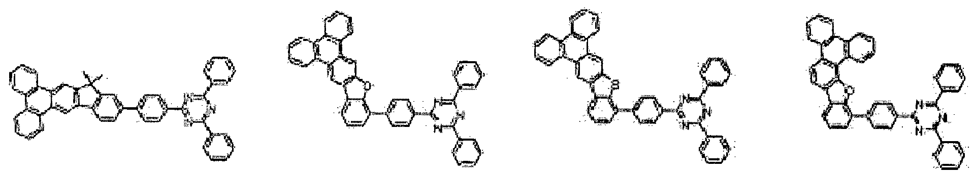
- organic compounds represented by a combination of moieties represented:
- X is CR a R b , SiR c R d , 0, S, SO or S0 2 ,
- Z are each independently N or CR e ,
- At least one of Z is N,
- R 1 to R 8 and R a to R e are each independently hydrogen, deuterium, a substituted or unsubstituted C1 to C20 alkyl group, a substituted or unsubstituted C6 to C30 aryl group, a substituted or unsubstituted C3 to C30 heteroaryl Groups or a combination thereof,
- L is a substituted or unsubstituted C1 to C20 alkylene group, a substituted or unsubstituted C6 to C30 arylene group, a substituted or unsubstituted C3 to C30 heteroarylene group, or a combination thereof,
- nl to n3 are each independently 0 or 1
- Adjacent two * of Chemical Formula 1 combines with two * of Chemical Formula 2 to form a fused ring.
- An organic optoelectronic device including at least one organic layer positioned therebetween, wherein the organic layer comprises the organic compound.
- a display device including the organic optoelectronic device is provided.
- FIG. 1 and 2 illustrate an organic light emitting diode according to an embodiment, respectively.
- substituted means that at least one hydrogen in a substituent or compound is a deuterium, halogen group, hydroxy group, amino group, substituted or unsubstituted C1 to C30 amine group, nitro group, substituted or unsubstituted C1 to C40 silyl group, C1 to C30 alkyl group, C1 to C10 alkylsilyl group, C3 to C30 cycloalkyl group C3 to C30 heterocycloalkyl group, C6 to C30 aryl group, C6 to C30 aryl group, C6 to C30
- C1 to C10 trifluoroalkyl group or cyano group such as heteroaryl group, C1 to C20 alkoxy group, fluoro group, trifluoromethyl group.
- substituted halogen group hydroxy group, amino group, substituted or unsubstituted C1 to C20 amine group, nitro group, substituted or unsubstituted C3 to C40 silyl group, C1 to C30 alkyl group, C1 to C10 alkylsilyl group, C3 to C1 to C10 such as C30 cycloalkyl group, C3 to C30 heterocycloalkyl group, C6 to C30 aryl group, C6 to C30 heteroaryl group, C1 to C20 alkoxy group, fluoro group, trifluoromethyl group, etc.
- Two adjacent substituents of the trifluoroalkyl group or the cyano group may be fused to form a ring.
- the substituted C6 to C30 aryl group may be fused to another adjacent substituted C6 to C30 aryl group to form a substituted or unsubstituted fluorene ring.
- hetero means N in one functional group, unless otherwise defined. It contains 1 to 3 hetero atoms selected from the group consisting of O, S, P and Si, and the rest means carbon.
- an "alkyl group” is aliphatic.
- the alkyl group may be a "saturated alkyl group" which does not contain any double or triple bonds.
- the alkyl group may be an alkyl group of C1 to C30. More specifically, the alkyl group may be a C1 to C20 alkyl group or a C1 to C10 alkyl group.
- a C1 to C4 alkyl group means that the alkyl chain contains from 1 to 4 carbon atoms, with methyl, ethyl, propyl, iso-propyl, ⁇ -butyl, iso-butyl, sec-butyl and t-butyl Selected from the group consisting of:
- alkyl group examples include methyl group, ethyl group, propyl group, isopropyl group, butyl group, isobutyl group, t-butyl group, pentyl group, nucleosil group, cyclopropyl group, cyclobutyl group, cyclopentyl group and cyclohex It means a practical skill.
- an "aryl group” refers to a substituent in which all elements of a cyclic substituent have a p-orbital and these P-orbitals form a conjugate, and are monocyclic, polycyclic or Fused ring polycyclic (ie, rings that divide adjacent pairs of carbon atoms) functional groups.
- heteroaryl group '' means containing 1 to 3 heteroatoms selected from the group consisting of N, 0, S, P and Si in the aryl group, and the rest is carbon.
- each ring may include 1 to 3 heteroatoms.
- a substituted or unsubstituted C6 to C30 aryl group and / or a substituted or unsubstituted C2 to C30 heteroaryl group is a substituted or unsubstituted phenyl group, a substituted or unsubstituted naphthyl group, a substituted or unsubstituted anthra Senyl group, substituted or unsubstituted phenanthryl group, substituted or unsubstituted naphthacenyl group, substituted or unsubstituted pyrenyl group, substituted or unsubstituted biphenyl group, substituted or unsubstituted P-terphenyl group, substituted or unsubstituted Substituted m-terphenyl group, substituted or unsubstituted chrysenyl group, substituted or unsubstituted Triphenylenyl group, substituted or unsubstituted pery
- Imidazolyl group substituted or unsubstituted triazolyl group, substituted or unsubstituted oxazolyl group, substituted or unsubstituted thiazolyl group, substituted or unsubstituted oxadiazolyl group, substituted or unsubstituted thiadiazoleyl group , Substituted or unsubstituted pyridyl group, substituted or unsubstituted pyrimidinyl group, substituted or unsubstituted pyrazinyl group, substituted or unsubstituted triazinyl group, substituted or unsubstituted benzofuranyl group, substituted or unsubstituted Benzothiophenyl group, substituted or unsubstituted benzimidazolyl group, substituted or unsubstituted indolyl group, substituted or unsubstituted quinolinyl group, substituted or unsubstitute
- Naphthyridinyl group substituted or unsubstituted benzoxazineyl group, substituted or unsubstituted benzthiazinyl group, substituted or unsubstituted acridinyl group, substituted or unsubstituted
- Phenazineyl group substituted or unsubstituted phenothiazineyl group, substituted or unsubstituted
- It may be, but is not limited to, a dibenzofuranyl group, a substituted or unsubstituted dibenzothiophenyl group, a substituted or unsubstituted carbazole group, or a combination thereof.
- the hole characteristic refers to a characteristic capable of forming holes by donating electrons when an electric field is applied, and injecting holes formed at the anode into the light emitting layer having conductive properties along the HOMO level, It means a property that facilitates the movement of the hole formed in the light emitting layer to the anode and the movement in the light emitting impingement.
- electron talkability refers to a property that can receive electrons when an electric field is applied, and has conductivity characteristics along the LUMO level. It means a property that facilitates movement.
- An organic compound according to one embodiment is represented by a combination of a moiety represented by Chemical Formula 1 and a moiety represented by Chemical Formula.
- X is CR a R b , SiR c R d , O, S, SO or S0 2 ,
- Z are each independently N or CR e ,
- At least one of Z is N,
- R 1 to R 8 and R a to R e are each independently hydrogen, deuterium, a substituted or unsubstituted C1 to C20 alkyl group, a substituted or unsubstituted C6 to C30 aryl group, a substituted or unsubstituted C3 to C30 heteroaryl Groups or a combination thereof,
- L is a substituted or unsubstituted C1 to C20 alkylene group, a substituted or unsubstituted C6 to C30 arylene group, a substituted or unsubstituted C3 to C30 heteroarylene group, or a combination thereof,
- nl to n3 are each independently 0 or 1
- Adjacent two * of Chemical Formula 1 combines with two * of Chemical Formula 2 to form a fused ring.
- the organic compound may be represented by, for example, the following Chemical Formula 3 or the following Chemical Formula 4, depending on the bonding position of the moiety represented by Chemical Formula 1 and the moiety represented by Chemical Formula 2.
- the organic compound includes indenotriphenylene and at least one nitrogen-containing heteroaryl group.
- the organic compound may include a ring containing at least one nitrogen, and thus may have a structure in which electrons are easily received when an electric field is applied, thereby lowering a driving voltage of the organic optoelectronic device to which the organic compound is applied.
- the organic compound includes an indenotriphenylene portion, which is easy to receive holes, and a nitrogen-containing ring portion, which is easy to accept electrons, to form a bipolar structure, thereby properly balancing the flow of holes and electrons.
- the efficiency of the organic optoelectronic device to which the organic compound is applied can be improved.
- the organic compound may exhibit excellent bipolar characteristics by appropriately localizing the indenotriphenylene portion susceptible to holes and the portion susceptible to electrons and controlling the flow of the conjugated system. Accordingly, the lifespan of the organic optoelectronic device to which the organic compound is applied can be improved.
- the organic compound may have a structure capable of effectively preventing stacking of organic compounds, thereby lowering process stability and lowering deposition temperature. .
- the moiety represented by Formula 2 may be, for example, represented by one of Formula 2 ′ I to Formula 2-III:
- X 1 , X 2 , X 3 , Z, R 5 to R 8 , R a to R e , L, nl to n 3 are as described above.
- X 1 and X 2 are each independently CR a R b or SiR c R d , X 3 is 0, S, SO or S0 2 , Z, R 5 to R 8 , to R e , L, nl to n3 are as described above.
- Formula 2 may be represented by, for example, a combination selected from Formula 2a and Group 1 below.
- L of Formula 2 may be, for example, a substituted or unsubstituted C6 to C30 arylene group, for example, a substituted or unsubstituted phenylene group, a substituted or unsubstituted biphenylene group, or a substituted or unsubstituted terphenylene group. It is not limited to this.
- R 1 to R 4 of Formula 1 may each independently be hydrogen, deuterium or a substituted or unsubstituted C1 to C20 alkyl group.
- the organic compound may be, for example, a compound listed in Group 2, but is not limited thereto.
- the organic compound may have a LUMO energy of about -2.0 to -2.5 eV. By having LUMO energy of the said range, an electron injection characteristic can be improved.
- the organic optoelectronic device is not particularly limited as long as the device can switch electrical energy and light energy. Examples thereof include an organic photoelectric device, an organic light emitting device, an organic solar cell, and an organic photosensitive drum.
- an organic optoelectronic device 100 includes an anode 120 and a cathode 110 facing each other, and an organic layer 105 positioned between the anode 120 and the cathode 1 10. It includes.
- the anode 120 may be made of a high work function conductor, for example, to facilitate hole injection, and may be made of metal, metal oxide, and / or conductive polymer, for example.
- the anode 120 is, for example, a metal such as nickel, platinum, vanadium, chromium, copper, zinc, gold or an alloy thereof; Zinc oxide, indium oxide, indium tin oxide ( ⁇ ),
- Metal oxides such as rhodium zinc oxide (IZO); Combinations of oxides with metals such as ZnO and A1 or Sn0 2 and Sb; Poly (3-methylthiophene), poly (3,4- (ethylene-1,2- Conductive polymers such as dioxy) thiophene Xpolyehtylenedioxythiophene (PEDT), polypyrrole and polyaniline, and the like, but are not limited thereto.
- Cathode 110 may be made of a low work function conductor, for example, to facilitate residue injection, and may be made of a metal, metal oxide, and / or conductive polymer, for example.
- Metals such as potassium, titanium, indium, yttrium, lithium, gadolinium, aluminum, silver, tin, lead, cesium, barium, or alloys thereof; Multilayer structure materials such as LiF / Al, Li0 2 / Al, LiF / Ca, LiF / Al, and BaF 2 / Ca, but are not limited thereto.
- the organic layer 105 includes a light emitting layer 130 including the above-described organic compound.
- the light emitting layer 130 may include the above-described organic compound alone, may include at least two kinds of the above-described organic compounds in combination, or may include the above-mentioned organic compound and other compounds in combination.
- the above-mentioned organic compound and other compounds are mixed and included, for example, it may be included in the form of a host and a dopant, and the above-described organic compound may be included as a host, for example.
- the host can be, for example, a phosphorescent host or a fluorescent host, for example a phosphorescent host.
- the dopant may be an inorganic, organic, or inorganic compound, and may be selected from known dopants.
- the organic light emitting diode 200 may have holes in addition to the light emitting layer 130.
- the hole auxiliary layer 140 may further increase hole injection and / or hole mobility between the anode 120 and the light emitting layer 130 and block electrons.
- the hole auxiliary layer 140 may be, for example, a hole transport layer, a hole injection layer, and / or an electron blocking layer, and may include at least one layer.
- the organic compound described above may be included in the emission layer 130 and / or the hole auxiliary layer 140.
- FIG. 1 In addition, in one embodiment of the present invention in FIG. 1
- the organic thin film layer 105 may further be an organic light emitting device further including an auxiliary electron transport layer, an electron transport layer, an electron injection layer, an auxiliary hole transport layer, a hole injection layer, and the like.
- the above-mentioned organic compound may be an auxiliary electron transport layer, an electron transport layer, an electron injection layer, an auxiliary hole transport layer and / or included in or additionally included in the light emitting layer 130 and / or the hole auxiliary layer 140.
- the organic light emitting diodes 100 and 200 may include a dry film method such as an anode or a cathode formed on a substrate and then vacuum evaporation, sputtering, plasma plating and ion plating; Or after forming an organic layer by wet coating such as spin coating, slit coating, dipping, flow coating, and inkjet printing, and the like, and thereon It can be prepared by forming a cathode or an anode.
- the organic light emitting diode described above may be applied to an organic light emitting diode display.
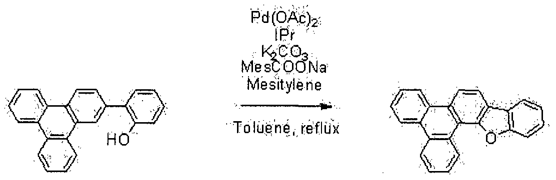
- Example 5 Synthesis of Compound 12 In a nitrogen environment, 20 g (55.2 mmol) of compound l-4 are dissolved in 200 mL of tetrahydrofuran (THF), followed by 2-chloro-4,6-diphenylpyrimidine. 14.7 g (55.2 mmol) and
- An organic light emitting device was manufactured using Compound 4 obtained in Example 1 as a host and Ir (PPy) 3 as a dopant.
- a positive electrode [pi] was used to a thickness of 1000 A
- a negative electrode a thickness of 1000 A of aluminum (A1) ol was used.
- the anode is 15 Q / cm 2
- the sheet resistance value of bedroomsn ⁇ glass substrate was cut into 50 mm X 50 mm X 0.7 mm, ultrasonically cleaned in acetone, isopropyl alcohol and pure water for 15 minutes, and then used by UV ozone cleaning for 30 minutes.
- N4'-di (naphthalen-l-yl) -N4, N4'-diphenylbiphenyl-4,4'-dia ⁇ (subject to vacuum of 650x lO-7Pa and deposition rate of 0.1 to 0.3 nm / s on the substrate)
- NPB 80 nm
- a light emitting layer having a film thickness of 300 A was formed using the compound 4 obtained in Example 1 under the same vacuum deposition conditions.
- Ir (PPy) 3 which is a phosphorescent dopant, was simultaneously deposited.
- Bis (2-methyl-8-quinolinolate) -4- (phenylphenolato) alummium (BAlq) was deposited on the emission layer to form a hole blocking layer having a thickness of 50 A.
- Alq3 was deposited under the same vacuum deposition conditions to form an electron transport layer having a thickness of 200 A.
- An organic photoelectric device was manufactured by sequentially depositing LiF and A1 as a cathode on the electron transport layer.
- the structure of the organic photoelectric device is ⁇ / NPB (80 nm) / EML ( Compound 4 (93 parts by weight 0/0) + Ir (PPy ) 3 (7 parts by weight 0 / o), 30 nm) / Balq (5 nm) / It was produced in the structure of Alq3 (20 nm) / LiF (1 nm) I Al (100 nm).
- Example 10 an organic light emitting diode was manufactured according to the same method as Example 1 except for using the compound 6 of Example 2 instead of the compound 4 of Example 1.
- Example 10 the organic light emitting device was manufactured in the same manner as in Example 1, except that Compound 7 of Example 3 was used instead of Compound 4 of Example 1.
- An organic light emitting diode was manufactured according to the same method as Example 10 except for using the compound 8 of Example 4 instead of the compound 4 of Example 1.
- An organic light emitting diode was manufactured according to the same method as Example 10 except for using the compound 12 of Example 5 instead of the compound 4 of Example 1.
- Example 15
- An organic light emitting diode was manufactured according to the same method as Example 10 except for using the compound 20 of Example 6 instead of the compound 4 of Example 1.
- An organic light emitting diode was manufactured according to the same method as Example 10 except for using the compound 44 of Example 7 instead of the compound 4 of Example 1.
- An organic light emitting diode was manufactured according to the same method as Example 10 except for using the compound 52 of Example 8 instead of the compound 4 of Example 1.
- An organic light emitting diode was manufactured according to the same method as Example 10 except for using Compound 60 of Example 9 instead of Compound 4 of Example 1.
- An organic light emitting diode was manufactured according to the same method as Example 10 except for using CBP instead of Compound 4 of Example 1.
- the structure of the CBP is described below.
- An organic light emitting diode was manufactured according to the same method as Example 10 except for using HOST1 instead of Compound 4 of Example 1.
- the structure of HOST1 is described below.
- An organic light emitting diode was manufactured according to the same method as Example 10 except for using HOST2 instead of Compound 4 of Example 1.
- the structure of HOST2 is described below.
- NPB, BAlq, CBP, Ir (PPy) 3, HOST 1 and HOST 2 used in the organic light emitting device fabrication is as follows.
- the current value flowing through the unit device was measured using a current-voltmeter (Keithley 2400) while increasing the voltage from 0V to 10V, and the measured current value was divided by the area to obtain a result.
- the luminance was measured by using a luminance meter (Minolta Cs-IOOOA) while increasing the voltage from 0V to 10V to obtain a result.
- a luminance meter Minolta Cs-IOOOA
- the current efficiency (cd / A) of the same current density (10 mA / cm 2) was calculated using the brightness, current density and voltage measured from (1) and (2) above.
- the organic light emitting diode according to Example 11 or Example 12 including Compound 6 or Compound 7 containing fluorine 3 ⁇ 41 group has the most excellent efficiency and low driving voltage.
- the present invention is not limited to the above embodiments, but may be manufactured in various forms, and a person skilled in the art to which the present invention pertains has another specific form without changing the technical spirit or essential features of the present invention. It will be appreciated that the present invention may be practiced as. Therefore, it should be understood that the embodiments described above are exemplary in all respects and not restrictive.
Landscapes
- Chemical & Material Sciences (AREA)
- Organic Chemistry (AREA)
- Engineering & Computer Science (AREA)
- Materials Engineering (AREA)
- Physics & Mathematics (AREA)
- Spectroscopy & Molecular Physics (AREA)
- Optics & Photonics (AREA)
- Electroluminescent Light Sources (AREA)
- Pyridine Compounds (AREA)
- Plural Heterocyclic Compounds (AREA)
Abstract
Description


Claims


Priority Applications (4)
| Application Number | Priority Date | Filing Date | Title |
|---|---|---|---|
| JP2016525262A JP6335288B2 (ja) | 2013-07-10 | 2014-02-20 | 有機化合物、有機光電子素子および表示装置 |
| CN201480039630.8A CN105377822B (zh) | 2013-07-10 | 2014-02-20 | 有机组合物、有机光电子元件及显示装置 |
| US14/786,379 US10032990B2 (en) | 2013-07-10 | 2014-02-20 | Organic composition, and organic optoelectronic element and display device |
| EP14823854.6A EP3020708B1 (en) | 2013-07-10 | 2014-02-20 | Organic compound, and organic optoelectronic element and display device |
Applications Claiming Priority (2)
| Application Number | Priority Date | Filing Date | Title |
|---|---|---|---|
| KR10-2013-0081176 | 2013-07-10 | ||
| KR1020130081176A KR101627761B1 (ko) | 2013-07-10 | 2013-07-10 | 유기 화합물, 유기 광전자 소자 및 표시 장치 |
Publications (1)
| Publication Number | Publication Date |
|---|---|
| WO2015005559A1 true WO2015005559A1 (ko) | 2015-01-15 |
Family
ID=52280207
Family Applications (1)
| Application Number | Title | Priority Date | Filing Date |
|---|---|---|---|
| PCT/KR2014/001391 Ceased WO2015005559A1 (ko) | 2013-07-10 | 2014-02-20 | 유기 화합물, 유기 광전자 소자 및 표시 장치 |
Country Status (6)
| Country | Link |
|---|---|
| US (1) | US10032990B2 (ko) |
| EP (1) | EP3020708B1 (ko) |
| JP (1) | JP6335288B2 (ko) |
| KR (1) | KR101627761B1 (ko) |
| CN (1) | CN105377822B (ko) |
| WO (1) | WO2015005559A1 (ko) |
Cited By (10)
| Publication number | Priority date | Publication date | Assignee | Title |
|---|---|---|---|---|
| CN105801430A (zh) * | 2015-01-19 | 2016-07-27 | 机光科技股份有限公司 | 菲并[9,10-b]联亚四苯衍生物以及其用途 |
| JP2016155797A (ja) * | 2014-12-30 | 2016-09-01 | 機光科技股▲分▼有限公司 | 有機材料およびそれを用いた有機エレクトロルミネッセンス素子 |
| US20160380207A1 (en) * | 2015-06-29 | 2016-12-29 | Feng-wen Yen | Triphenylene-based fused biscarbazole derivative and use thereof |
| JP2017513242A (ja) * | 2014-04-04 | 2017-05-25 | エルジー・ケム・リミテッド | 有機発光素子 |
| JP2017517486A (ja) * | 2014-04-04 | 2017-06-29 | エルジー・ケム・リミテッド | 複素環化合物及びこれを含む有機発光素子 |
| TWI601710B (zh) * | 2015-01-26 | 2017-10-11 | 機光科技股份有限公司 | 化合物及使用其的有機電激發光裝置 |
| JP2018507174A (ja) * | 2014-12-24 | 2018-03-15 | ドゥーサン コーポレイション | 有機化合物及びこれを含む有機電界発光素子 |
| US10381572B2 (en) | 2014-04-04 | 2019-08-13 | Lg Chem, Ltd. | Heterocyclic compound and organic light-emitting element comprising same |
| US11271167B2 (en) | 2014-04-04 | 2022-03-08 | Lg Chem, Ltd. | Organic light-emitting device |
| EP3259786B1 (en) * | 2015-02-18 | 2023-08-30 | Novaled GmbH | Semiconducting material and naphtofurane matrix compound for it |
Families Citing this family (22)
| Publication number | Priority date | Publication date | Assignee | Title |
|---|---|---|---|---|
| US9929349B2 (en) * | 2014-12-08 | 2018-03-27 | Samsung Display Co., Ltd. | Organic light emitting device and display device including the same |
| KR102041588B1 (ko) * | 2016-09-29 | 2019-11-06 | 삼성에스디아이 주식회사 | 유기 광전자 소자용 화합물, 유기 광전자 소자용 조성물, 유기 광전자 소자 및 표시 장치 |
| KR101970000B1 (ko) * | 2016-10-12 | 2019-04-17 | 삼성에스디아이 주식회사 | 유기 광전자 소자용 화합물, 유기 광전자 소자 및 표시 장치 |
| US10103337B1 (en) * | 2017-04-28 | 2018-10-16 | Feng-wen Yen | Organic electroluminescent material and using the same |
| CN107163057A (zh) * | 2017-06-30 | 2017-09-15 | 中节能万润股份有限公司 | 一种含有氮杂二苯并呋喃并邻菲罗啉结构的oled材料、其制备方法及应用 |
| KR102020029B1 (ko) * | 2017-07-10 | 2019-09-10 | 주식회사 엘지화학 | 신규한 헤테로 고리 화합물 및 이를 이용한 유기발광 소자 |
| WO2019013509A1 (ko) * | 2017-07-10 | 2019-01-17 | 주식회사 엘지화학 | 신규한 헤테로 고리 화합물 및 이를 이용한 유기발광 소자 |
| CN110997648B (zh) * | 2017-08-10 | 2023-12-19 | 东曹株式会社 | 稠环化合物 |
| US10428269B2 (en) | 2017-12-27 | 2019-10-01 | Feng-wen Yen | Indenotriphenylene derivative and organic electroluminescence device using the same |
| KR102217250B1 (ko) * | 2018-06-12 | 2021-02-18 | 삼성에스디아이 주식회사 | 유기 광전자 소자용 조성물, 유기 광전자 소자 및 표시 장치 |
| EP3582280B1 (en) * | 2018-06-14 | 2024-03-20 | Novaled GmbH | Organic material for an electronic optoelectronic device and electronic device comprising the organic material |
| US11236075B2 (en) * | 2018-12-17 | 2022-02-01 | Luminescence Technology Corp. | Organic compound and organic electroluminescence device using the same |
| US11296282B2 (en) * | 2018-12-17 | 2022-04-05 | Luminescence Technology Corp. | Organic compound and organic electroluminescence device using the same |
| EP3670510A3 (en) * | 2018-12-20 | 2020-07-01 | Duk San Neolux Co., Ltd. | Benzo[b]naphtho[2,3-d]furanyl- or benzo[b]naphtho[2,3-d]thiophenyl-triazine compounds for organic electronic elements |
| KR102397215B1 (ko) * | 2018-12-20 | 2022-05-12 | 덕산네오룩스 주식회사 | 유기전기 소자용 화합물, 이를 이용한 유기전기소자 및 그 전자 장치 |
| US11108001B2 (en) * | 2019-01-17 | 2021-08-31 | Luminescence Technology Corp. | Organic compound and organic electroluminescence device using the same |
| EP3992190A4 (en) | 2019-06-28 | 2023-07-19 | Samsung SDI Co., Ltd. | COMPOUND FOR ORGANIC OPTOELECTRONIC DIODE, COMPOSITION FOR ORGANIC OPTOELECTRONIC DIODE, ORGANIC OPTOELECTRONIC DIODE AND INDICATOR |
| KR102701842B1 (ko) * | 2019-06-28 | 2024-09-02 | 삼성에스디아이 주식회사 | 유기 광전자 소자용 화합물, 유기 광전자 소자용 조성물, 유기 광전자 소자 및 표시 장치 |
| KR102442580B1 (ko) * | 2020-04-09 | 2022-09-13 | 주식회사 엘지화학 | 신규한 화합물 및 이를 이용한 유기 발광 소자 |
| WO2021206502A1 (ko) * | 2020-04-09 | 2021-10-14 | 주식회사 엘지화학 | 유기 발광 소자 |
| TWI792166B (zh) * | 2021-01-29 | 2023-02-11 | 機光科技股份有限公司 | 有機化合物和以其作為材料的紅光有機發光裝置 |
| CN116730996A (zh) * | 2022-03-01 | 2023-09-12 | 宁波卢米蓝新材料有限公司 | 一种有机化合物、有机电致发光材料及其应用 |
Citations (3)
| Publication number | Priority date | Publication date | Assignee | Title |
|---|---|---|---|---|
| JP2002043061A (ja) * | 2000-07-31 | 2002-02-08 | Mitsui Chemicals Inc | 炭化水素化合物および有機電界発光素子 |
| US20060115680A1 (en) * | 2004-11-29 | 2006-06-01 | Seok-Hwan Hwang | Phenylcarbazole-based compound and organic electroluminescent device employing the same |
| US20130099206A1 (en) * | 2011-10-19 | 2013-04-25 | Samsung Mobile Display Co., Ltd. | Heterocyclic compound, organic light-emitting diode including the heterocyclic compound, and flat display device including the organic light-emitting diode |
Family Cites Families (18)
| Publication number | Priority date | Publication date | Assignee | Title |
|---|---|---|---|---|
| TWI501943B (zh) | 2007-08-08 | 2015-10-01 | Universal Display Corp | 磷光發光二極體內之單聯伸三苯發色團 |
| JP2009114068A (ja) | 2007-11-01 | 2009-05-28 | Canon Inc | トリフェニレン化合物及びこれを用いた有機発光素子 |
| TWI448534B (zh) * | 2009-09-28 | 2014-08-11 | Ritdisplay Corp | 有機電致發光元件 |
| KR101724304B1 (ko) | 2009-10-16 | 2017-04-10 | 에스에프씨 주식회사 | 축합방향족 화합물 및 이를 포함하는 유기전계발광소자 |
| KR101134575B1 (ko) | 2009-11-17 | 2012-04-16 | 주식회사 이엘엠 | 유기 전기 발광 조성물 및 이를 포함하는 유기 전기 발광 소자 |
| US8968887B2 (en) * | 2010-04-28 | 2015-03-03 | Universal Display Corporation | Triphenylene-benzofuran/benzothiophene/benzoselenophene compounds with substituents joining to form fused rings |
| KR101196093B1 (ko) | 2010-05-06 | 2012-11-01 | 주식회사 두산 | 페난스로카바졸 화합물 및 이를 이용한 유기 전계 발광 소자 |
| KR101218029B1 (ko) | 2010-05-06 | 2013-01-02 | 주식회사 두산 | 방향족 아민을 포함하는 트리페닐렌계 화합물 및 이를 포함하는 유기 전계 발광 소자 |
| JP5735241B2 (ja) | 2010-09-08 | 2015-06-17 | ユー・ディー・シー アイルランド リミテッド | 有機電界発光素子及び電荷輸送材料 |
| JP5729957B2 (ja) | 2010-09-29 | 2015-06-03 | キヤノン株式会社 | ジベンゾチオフェン化合物およびそれを有する有機発光素子 |
| JP5773638B2 (ja) | 2010-12-24 | 2015-09-02 | キヤノン株式会社 | 縮合多環化合物及びこれを用いた有機発光素子 |
| KR101866851B1 (ko) | 2010-12-24 | 2018-06-14 | 에스에프씨 주식회사 | 이형고리 화합물 및 이를 포함하는 유기전계발광소자 |
| JP5804797B2 (ja) * | 2011-06-28 | 2015-11-04 | キヤノン株式会社 | ベンゾトリフェニレノフラン化合物およびそれを有する有機発光素子 |
| KR101366368B1 (ko) | 2011-07-08 | 2014-02-21 | 주식회사 두산 | 신규 유기 전계 발광 화합물 및 이를 포함하는 유기 전계 발광 소자 |
| KR20130007951A (ko) | 2011-07-11 | 2013-01-21 | 주식회사 두산 | 트리페닐렌계 화합물 및 이를 이용한 유기 전계 발광 소자 |
| KR101470055B1 (ko) | 2011-07-11 | 2014-12-08 | 주식회사 두산 | 트리페닐렌계 화합물 및 이를 이용한 유기 전계 발광 소자 |
| KR101618683B1 (ko) | 2013-05-16 | 2016-05-09 | 제일모직 주식회사 | 유기 화합물, 유기 광전자 소자 및 표시 장치 |
| KR102078365B1 (ko) * | 2013-07-01 | 2020-04-03 | 삼성디스플레이 주식회사 | 유기 발광 장치 |
-
2013
- 2013-07-10 KR KR1020130081176A patent/KR101627761B1/ko active Active
-
2014
- 2014-02-20 WO PCT/KR2014/001391 patent/WO2015005559A1/ko not_active Ceased
- 2014-02-20 US US14/786,379 patent/US10032990B2/en active Active
- 2014-02-20 CN CN201480039630.8A patent/CN105377822B/zh active Active
- 2014-02-20 EP EP14823854.6A patent/EP3020708B1/en active Active
- 2014-02-20 JP JP2016525262A patent/JP6335288B2/ja active Active
Patent Citations (3)
| Publication number | Priority date | Publication date | Assignee | Title |
|---|---|---|---|---|
| JP2002043061A (ja) * | 2000-07-31 | 2002-02-08 | Mitsui Chemicals Inc | 炭化水素化合物および有機電界発光素子 |
| US20060115680A1 (en) * | 2004-11-29 | 2006-06-01 | Seok-Hwan Hwang | Phenylcarbazole-based compound and organic electroluminescent device employing the same |
| US20130099206A1 (en) * | 2011-10-19 | 2013-04-25 | Samsung Mobile Display Co., Ltd. | Heterocyclic compound, organic light-emitting diode including the heterocyclic compound, and flat display device including the organic light-emitting diode |
Non-Patent Citations (2)
| Title |
|---|
| See also references of EP3020708A4 * |
| ZHOU, Y. ET AL.: "Selective Oxidative Cyclization by FeC13 in the Construction of 10H-Indeno [1,2-b]triphynylene Skeletons in Polycyclic Aromatic Hydrocarbons", JOURNAL OF ORGANIC CHEMISTRY, vol. 71, no. 18, 1 August 2006 (2006-08-01), pages 6822 - 6828, XP055306629 * |
Cited By (21)
| Publication number | Priority date | Publication date | Assignee | Title |
|---|---|---|---|---|
| US11342508B2 (en) | 2014-04-04 | 2022-05-24 | Lg Chem, Ltd. | Organic light-emitting device |
| US10510963B2 (en) | 2014-04-04 | 2019-12-17 | Lg Chem, Ltd. | Heterocyclic compound and organic light-emitting element comprising same |
| US11877510B2 (en) | 2014-04-04 | 2024-01-16 | Lg Chem, Ltd. | Heterocyclic compound and organic light-emitting element comprising same |
| JP2017513242A (ja) * | 2014-04-04 | 2017-05-25 | エルジー・ケム・リミテッド | 有機発光素子 |
| JP2017517486A (ja) * | 2014-04-04 | 2017-06-29 | エルジー・ケム・リミテッド | 複素環化合物及びこれを含む有機発光素子 |
| US11362280B2 (en) | 2014-04-04 | 2022-06-14 | Lg Chem, Ltd. | Organic light-emitting device |
| US10916710B2 (en) | 2014-04-04 | 2021-02-09 | Lg Chem, Ltd. | Heterocyclic compound and organic light-emitting element comprising same |
| US11271167B2 (en) | 2014-04-04 | 2022-03-08 | Lg Chem, Ltd. | Organic light-emitting device |
| US10964892B2 (en) | 2014-04-04 | 2021-03-30 | Lg Chem, Ltd. | Heterocyclic compound and organic light-emitting device comprising same |
| US10381572B2 (en) | 2014-04-04 | 2019-08-13 | Lg Chem, Ltd. | Heterocyclic compound and organic light-emitting element comprising same |
| JP2018507174A (ja) * | 2014-12-24 | 2018-03-15 | ドゥーサン コーポレイション | 有機化合物及びこれを含む有機電界発光素子 |
| US10916709B2 (en) | 2014-12-24 | 2021-02-09 | Doosan Solus Co., Ltd. | Organic compound and organic electroluminescent element comprising same |
| US11832514B2 (en) | 2014-12-24 | 2023-11-28 | Solus Advanced Materials Co., Ltd. | Organic compound and organic electroluminescent element comprising same |
| US11997924B2 (en) | 2014-12-24 | 2024-05-28 | Solus Advanced Materials Co., Ltd. | Organic compound and organic electroluminescent element comprising same |
| JP2016155797A (ja) * | 2014-12-30 | 2016-09-01 | 機光科技股▲分▼有限公司 | 有機材料およびそれを用いた有機エレクトロルミネッセンス素子 |
| CN105801430B (zh) * | 2015-01-19 | 2018-08-28 | 机光科技股份有限公司 | 菲并[9,10-b]联亚四苯衍生物以及其用途 |
| CN105801430A (zh) * | 2015-01-19 | 2016-07-27 | 机光科技股份有限公司 | 菲并[9,10-b]联亚四苯衍生物以及其用途 |
| US10164194B2 (en) * | 2015-01-26 | 2018-12-25 | Luminescence Technology Corporation | Compound for organic electroluminescent device |
| TWI601710B (zh) * | 2015-01-26 | 2017-10-11 | 機光科技股份有限公司 | 化合物及使用其的有機電激發光裝置 |
| EP3259786B1 (en) * | 2015-02-18 | 2023-08-30 | Novaled GmbH | Semiconducting material and naphtofurane matrix compound for it |
| US20160380207A1 (en) * | 2015-06-29 | 2016-12-29 | Feng-wen Yen | Triphenylene-based fused biscarbazole derivative and use thereof |
Also Published As
| Publication number | Publication date |
|---|---|
| KR20150007139A (ko) | 2015-01-20 |
| EP3020708A4 (en) | 2017-03-01 |
| JP6335288B2 (ja) | 2018-05-30 |
| JP2016525512A (ja) | 2016-08-25 |
| CN105377822B (zh) | 2017-05-31 |
| EP3020708B1 (en) | 2021-04-07 |
| US10032990B2 (en) | 2018-07-24 |
| KR101627761B1 (ko) | 2016-06-07 |
| EP3020708A1 (en) | 2016-05-18 |
| US20160072073A1 (en) | 2016-03-10 |
| CN105377822A (zh) | 2016-03-02 |
Similar Documents
| Publication | Publication Date | Title |
|---|---|---|
| JP6335288B2 (ja) | 有機化合物、有機光電子素子および表示装置 | |
| JP6431530B2 (ja) | 有機光電子素子用発光材料、有機光電子素子および表示装置 | |
| JP6257113B2 (ja) | 有機化合物、有機光電子素子および表示装置 | |
| KR101627755B1 (ko) | 유기 화합물, 유기 광전자 소자 및 표시 장치 | |
| JP6402192B2 (ja) | 有機光電子素子用組成物、有機光電子素子および表示装置 | |
| US10147891B2 (en) | Organic compound, organic optoelectronic device, and display device | |
| KR101653338B1 (ko) | 유기 화합물, 유기 광전자 소자 및 표시 장치 | |
| WO2015156449A1 (ko) | 유기 화합물, 조성물, 유기 광전자 소자 및 표시 장치 | |
| KR20140135532A (ko) | 유기 화합물, 유기 광전자 소자 및 표시 장치 | |
| WO2015186882A1 (ko) | 유기 화합물, 유기 광전자 소자 및 표시 장치 | |
| WO2017099326A1 (ko) | 유기 광전자 소자용 화합물, 유기 광전자 소자 및 표시 장치 | |
| KR102061246B1 (ko) | 유기 광전자 소자용 화합물, 유기 광전자 소자용 조성물, 유기 광전자 소자 및 표시 장치 | |
| KR102162401B1 (ko) | 유기 광전자 소자용 조성물, 유기 광전자 소자 및 표시 장치 | |
| KR102008895B1 (ko) | 유기 광전자 소자용 화합물, 유기 광전자 소자 및 표시 장치 | |
| KR102146791B1 (ko) | 유기 광전자 소자용 화합물, 유기 광전자 소자 및 표시 장치 | |
| KR102027962B1 (ko) | 유기 광전자 소자용 화합물, 유기 광전자 소자 및 표시 장치 | |
| KR101733651B1 (ko) | 화합물, 이를 포함하는 유기 광전자 소자 및 표시장치 | |
| KR20150024669A (ko) | 화합물, 이를 포함하는 유기발광소자 및 상기 유기발광소자를 포함하는 표시장치 |
Legal Events
| Date | Code | Title | Description |
|---|---|---|---|
| 121 | Ep: the epo has been informed by wipo that ep was designated in this application |
Ref document number: 14823854 Country of ref document: EP Kind code of ref document: A1 |
|
| WWE | Wipo information: entry into national phase |
Ref document number: 14786379 Country of ref document: US |
|
| ENP | Entry into the national phase |
Ref document number: 2016525262 Country of ref document: JP Kind code of ref document: A |
|
| NENP | Non-entry into the national phase |
Ref country code: DE |
|
| WWE | Wipo information: entry into national phase |
Ref document number: 2014823854 Country of ref document: EP |