WO2015012239A1 - Procédé et dispositif de production d'élément électroluminescent organique - Google Patents
Procédé et dispositif de production d'élément électroluminescent organique Download PDFInfo
- Publication number
- WO2015012239A1 WO2015012239A1 PCT/JP2014/069249 JP2014069249W WO2015012239A1 WO 2015012239 A1 WO2015012239 A1 WO 2015012239A1 JP 2014069249 W JP2014069249 W JP 2014069249W WO 2015012239 A1 WO2015012239 A1 WO 2015012239A1
- Authority
- WO
- WIPO (PCT)
- Prior art keywords
- organic
- sealing member
- substrate
- adhesive layer
- adhesive
- Prior art date
- Legal status (The legal status is an assumption and is not a legal conclusion. Google has not performed a legal analysis and makes no representation as to the accuracy of the status listed.)
- Ceased
Links
Images




Classifications
-
- H—ELECTRICITY
- H10—SEMICONDUCTOR DEVICES; ELECTRIC SOLID-STATE DEVICES NOT OTHERWISE PROVIDED FOR
- H10K—ORGANIC ELECTRIC SOLID-STATE DEVICES
- H10K71/00—Manufacture or treatment specially adapted for the organic devices covered by this subclass
-
- H—ELECTRICITY
- H10—SEMICONDUCTOR DEVICES; ELECTRIC SOLID-STATE DEVICES NOT OTHERWISE PROVIDED FOR
- H10K—ORGANIC ELECTRIC SOLID-STATE DEVICES
- H10K59/00—Integrated devices, or assemblies of multiple devices, comprising at least one organic light-emitting element covered by group H10K50/00
- H10K59/80—Constructional details
- H10K59/87—Passivation; Containers; Encapsulations
- H10K59/871—Self-supporting sealing arrangements
- H10K59/8722—Peripheral sealing arrangements, e.g. adhesives, sealants
-
- H—ELECTRICITY
- H10—SEMICONDUCTOR DEVICES; ELECTRIC SOLID-STATE DEVICES NOT OTHERWISE PROVIDED FOR
- H10K—ORGANIC ELECTRIC SOLID-STATE DEVICES
- H10K77/00—Constructional details of devices covered by this subclass and not covered by groups H10K10/80, H10K30/80, H10K50/80 or H10K59/80
- H10K77/10—Substrates, e.g. flexible substrates
- H10K77/111—Flexible substrates
Definitions
- the present invention relates to a method for manufacturing an organic electroluminescent element and a manufacturing apparatus, and more particularly to a method for sealing an organic electroluminescent element.
- organic electroluminescence (hereinafter also referred to as organic EL) elements as self-luminous elements have attracted attention.
- a light emitting layer of an organic compound hereinafter also referred to as an organic light emitting layer or simply a light emitting layer
- the organic light emitting layer emits light by arranging the organic EL structure having the structure and supplying a current between the anode and the cathode.
- the roll-to-roll manufacturing method here refers to a substrate wound in a roll shape, an organic EL structure is formed on the substrate, and the substrate on which the organic EL structure is formed is wound around a roll again.
- the manufacturing method of a form is pointed out.
- the roll-to-roll manufacturing method has the advantage that production efficiency can be improved because continuous production is possible.
- the organic light emitting layer constituting the organic EL element is easily affected by moisture and oxygen, and if left in the air, the quality is deteriorated by moisture and oxygen. Therefore, in the manufacturing process of the organic EL element, an external environment called sealing is used. A step of forming a protective layer on the organic EL structure for reducing the influence is added.
- a sealing technique of the organic EL structure for example, a sheet-like sealing that blocks moisture and oxygen based on a flexible material mainly made of a plastic film so as to keep the flexibility of the organic EL structure.
- a technique is known in which a stop substrate is bonded to an organic EL structure using an adhesive having sealing performance to perform sealing (see, for example, Patent Document 1).
- a flexible organic EL element can be created by bonding a sheet-shaped sealing substrate to an organic EL structure.
- the sealing substrate in order to obtain the required sealing performance, it is required that the sealing substrate be uniformly bonded to the organic EL structure without bubbles or wrinkles.
- Patent Document 1 requires an operation of discharging a liquid resin material onto a substrate on which the organic EL structure is formed when sealing the organic EL structure. For this reason, the handling of the resin material (adhesive) at the time of sealing is not easy, and there is a risk of reducing the production efficiency.
- the present invention provides a method for producing an organic EL element capable of uniformly bonding a flexible sealing substrate having an adhesive layer formed in advance to an organic EL structure while suppressing bubbles and wrinkles, and It is an object to provide a manufacturing apparatus.
- the organic electroluminescence structure is sealed by bonding a sealing member to the organic electroluminescence structure having at least the first electrode, the organic functional layer including the light emitting layer, and the second electrode formed on the substrate.
- a method of manufacturing an organic electroluminescence device by stopping the sealing member, wherein the sealing member includes a flexible sealing substrate and a thermosetting adhesive previously formed on one surface of the sealing substrate.
- the adhesive layer includes a second step in which both of them are brought into close contact under a condition where the adhesive layer has a second adhesiveness higher than the first adhesive property, and a third step in which the adhesive layer is cured in this order.
- the organic electroluminescence structure and the sealing member are brought into close contact with each other at a first temperature
- the organic electroluminescence at a second temperature higher than the first temperature 4.
- Said 2nd temperature is 80 degreeC or more and 130 degrees C or less, The manufacturing method of the said organic electroluminescent element of 4 or 5 characterized by the above-mentioned.
- the organic electroluminescence structure is sealed by bonding a sealing member to the organic electroluminescence structure having at least the first electrode, the organic functional layer including the light emitting layer, and the second electrode formed on the substrate.
- a first treatment part that adheres both under the condition that the adhesive layer has first adhesiveness, the organic electroluminescence structure, and the sealing member And a second processing unit that causes the adhesive layer to adhere to each other under a condition that the second adhesiveness is higher than the first adhesiveness, and a third processing unit that cures the adhesive layer.
- the organic electroluminescence structure is sealed by bonding a sealing member to the organic electroluminescence structure having at least the first electrode, the organic functional layer including the light emitting layer, and the second electrode formed on the substrate.
- Apparatus for producing an organic electroluminescent device characterized by having an adhesion processing section for close contact with each other, and a curing treatment unit for curing the adhesive layer.
- a method for producing an organic EL element capable of uniformly bonding a flexible sealing substrate in which an adhesive layer is formed in advance to an organic EL structure while suppressing bubbles and wrinkles, and A manufacturing apparatus can be provided.
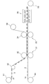
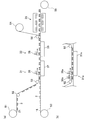
- FIG. 1 It is a schematic sectional drawing which shows an example of a structure of an organic EL element. It is a process line figure showing an example of the 1st process, the 2nd process, and the 3rd process concerning a 1st embodiment of a manufacturing method of an organic EL device concerning the present invention. It is the flowchart concerning 1st Embodiment and 2nd Embodiment of the manufacturing method of the organic EL element which concerns on this invention. (A) is a process line figure showing an example of the 1st process, the 2nd process, and the 3rd process concerning a 2nd embodiment of a manufacturing method of an organic EL device concerning the present invention.
- (B) is the partial process line figure which shows the 1st process of 2nd Embodiment, and the modification of a 2nd process. It is a process line figure showing the 1st process, the 2nd process, and the 3rd process concerning a 3rd embodiment of a manufacturing method of an organic EL device concerning the present invention. It is a flowchart which concerns on 3rd Embodiment of the manufacturing method of the organic EL element concerning this invention.
- Embodiments of the present invention will be described with reference to FIGS. 1 to 6, but the present invention is not limited to the following.
- the present invention provides the organic electroluminescence by bonding a sealing member to an organic electroluminescence structure having at least a first electrode, an organic functional layer including a light emitting layer, and a second electrode formed on a substrate.
- An adhesive layer containing an adhesive, and a surface side of the substrate on which the organic electroluminescence structure is formed and an adhesive layer side of the sealing member are opposed to each other, and the organic electroluminescence structure and the sealing
- the organic EL structure and the sealing member which is the sealing substrate on which the adhesive layer including the thermosetting adhesive is formed are bonded via the adhesive layer including the thermosetting adhesive. Adhering in a state where the adhesiveness of the layer is low makes it difficult for air bubbles to be included between the organic EL structure and the adhesive layer, and the adhesive layer is less likely to become wrinkles. That is, it becomes possible to adhere the organic EL structure and the sealing substrate while eliminating bubbles and wrinkles.
- the organic EL structure and the sealing substrate adhered to the organic EL structure are further adhered in a state where the adhesive layer is high in adhesive state.
- the uniformity of the adhesive force of the adhesive layer with the sealing substrate is improved.
- the organic EL element 1 manufactured according to the present invention includes an organic EL structure 2 provided on a substrate 16 and a sealing member 3 bonded to the organic EL structure 2.
- the organic EL structure 2 includes at least a first electrode 11, a second electrode 13, and an organic functional layer 12 including a light emitting layer, and includes a first electrode 11 provided on a substrate 16, a second electrode 11, and a second electrode 11.
- the organic functional layer 12 is sandwiched between the electrodes 13.
- the first electrode 11 and the second electrode 13 are a pair of an anode and a cathode.
- the sealing member 3 includes a flexible sealing substrate 15 and an adhesive layer 14 including a thermosetting adhesive formed in advance on one surface of the sealing substrate 15.
- the sealing substrate 15 has a support substrate and a barrier layer (both not shown).
- the substrate 16 is a member that serves as a support for the organic EL element 1.
- the substrate 16 is not limited to quartz, glass, plastic, or the like. In the case of a long strip, a flexible synthetic resin film is often used. When light is extracted from the substrate 16 side, the substrate is preferably transparent.
- the substrate 16 When the substrate 16 is made of a synthetic resin film, it can be formed of a film applied to a known organic EL element.
- a film applied to a known organic EL element For example, it can be formed of polyester such as polyethylene terephthalate (PET) or polyethylene naphthalate (PEN), polyethylene, or the like.
- PET polyethylene terephthalate
- PEN polyethylene naphthalate
- the first electrode 11 (anode) side is usually the observation side.
- an electrode material made of a metal, an alloy, an electrically conductive compound, or a mixture thereof having a large work function (4 eV or more) and a transmittance of 40% or more is preferably used.
- the first electrode anode
- a known substance can be used for the first electrode (anode).
- the substance described in Paragraph 0046 of JP2012-22783A, Paragraph 0077 of International Publication WO2011-132631 is used. Is possible.
- the second electrode 13 is connected to a power source and functions as, for example, a cathode.
- a known substance can be used.
- JP2012-22783A and paragraphs 0127 to 0130 of JP2012-128954A It is possible to use the substances described.
- the organic functional layer 12 is a light emitting layer (not shown) that emits light by recombination of holes injected from the first electrode 11 (anode) and electrons injected from the second electrode 13 (cathode). Contains.
- the organic functional layer 12 includes an electron transport layer, a hole transport layer, a hole injection layer (anode buffer layer), an electron injection layer (cathode buffer layer), a hole blocking layer, an electron blocking layer, and the like ( Any of them can be appropriately laminated.
- the light emitting layer is a layer that emits light by recombination of holes injected from the first electrode 11 (anode) and electrons injected from the second electrode 13 (cathode).
- the portion that emits light may be within the layer of the light emitting layer or at the interface between the light emitting layer and the adjacent layer.
- the light emitting layer may be a single layer or may be a multilayer using a plurality of light emitting layers. In the case of a multilayer structure, a non-light emitting intermediate layer may be provided between the light emitting layers.
- the organic functional layer 12 including the light emitting layer can be used as one light emitting unit, and a plurality of light emitting units can be stacked.
- the plurality of stacked light emitting units may have a non-light emitting intermediate layer between the light emitting units, and the intermediate layer may further include a charge generation layer.
- a known substance can be used for the light emitting layer constituting the organic functional layer 12, for example, paragraph 0022 of JP 2013-58673 A, paragraphs 0093 to 0096 of JP 2012-186212 A, It can be formed of a material that satisfies the conditions described in paragraph 0053 of JP 2012-22783, paragraph 0180 of JP 2009-37751 A, paragraph 0022 of JP 2013-89608 A.
- the hole transport layer has a role of moving holes to an effective recombination region and a role of blocking electrons locally as an energy barrier to strengthen light emission.
- the hole transport layer is made of a hole transport material having a function of transporting holes, and in a broad sense, a hole injection layer and an electron blocking layer are also included in the hole transport layer.
- the hole transport layer can be provided as a single layer or a plurality of layers. These are described in detail in Volume 2, Chapter 2, “Electrode Materials” (pages 123 to 166) of “Organic EL devices and their forefront of industrialization” (NTS Inc., issued on November 30, 1998). Are listed.
- a known substance can be used, for example, paragraphs 0148 to 0150 of JP 2013-84962 A, paragraph 0110 of JP 2013-128954 A, and so on. It is possible to use substances satisfying the conditions described in paragraphs 0083 to 0089 of JP-A-2013-89608 and paragraph 0048 of JP-A-2012-22783.
- the electron transport layer plays a role of moving holes to an effective recombination region and a role of blocking holes as an energy barrier and locally retaining light to enhance light emission.
- the electron transport layer is made of a material having a function of transporting electrons (electron transport material), and includes an electron injection layer and a hole blocking layer in a broad sense.
- the electron transport layer can be provided as a single layer or a plurality of layers. These are described in detail in “Organic EL elements and their industrialization front line” (issued by NTT, Inc. on November 30, 1998).
- Electrode buffer layer For the electron injection layer (cathode buffer layer) constituting the organic functional layer 12, a known substance can be used, for example, a substance described in paragraph 0100 of JP 2012-128954 A is used. Is possible.
- the hole blocking layer As the hole blocking layer constituting the organic functional layer 12, a known substance can be used. For example, the substances described in paragraphs 0143 to 0145 of JP 2013-84962 A can be used. is there.
- the hole blocking layer can be implemented using the one described in the electron transport layer.
- the hole blocking layer is preferably provided adjacent to the light emitting layer.
- the thickness of the hole blocking layer is preferably 3 to 100 nm, more preferably 5 to 30 nm.
- the sealing substrate 15 of the organic EL element 1 has a barrier layer (not shown) on the side in contact with the organic EL structure 2. Furthermore, a protective layer (not shown) may be provided on the barrier layer.
- the support substrate is preferably a flexible resin substrate, and examples thereof include a resin film and a transparent resin film.
- the support substrate may be a single body or a laminate, and can be appropriately selected as necessary.
- the barrier layer may be a single body or a laminate, and can be appropriately selected as necessary.
- the thickness of the support substrate is preferably 10 ⁇ m to 500 ⁇ m in consideration of handling at the time of manufacture, tensile strength, stress cracking resistance of the barrier layer, and the like.
- the water vapor permeability of the support substrate is preferably 0.01 g / m 2 ⁇ day or less in consideration of gas barrier properties and the like required for commercialization as an organic EL element.
- the water vapor permeability indicates a value measured mainly by the MOCON method by a method based on the JIS K7129B method (1992).
- the oxygen permeability of the support substrate is preferably 0.01 ml / m 2 ⁇ day ⁇ atm or less.
- the oxygen permeability is a value measured mainly by the MOCON method by a method based on the JIS K7126B method (1987).
- the rigidity (Young's modulus) of the support substrate is preferably 1 ⁇ 10 ⁇ 3 GPa to 80 GPa in consideration of handleability during manufacturing, tensile strength, stress cracking resistance of the barrier layer, and the like.
- the support substrate constituting the sealing substrate 15 used in the present invention is not particularly limited as long as it has flexibility and satisfies the above numerical values.
- This support substrate includes, for example, unstretched polypropylene (CPP), polyvinyl alcohol, which is a polymer film described in “New trends in functional packaging material development” (Toray Research Center, Inc.). (PVA), cellophane, expanded vinylon (OV), ethylene-vinyl alcohol copolymer (EVOH), ethylene-propylene copolymer, ethylene-acrylic acid copolymer, ethylene-methacrylic acid copolymer, vinylidene chloride (PVDC) ) Etc. can be used.
- this support substrate includes oriented polypropylene (OPP), oriented nylon (ONy), polyethylene terephthalate (PET), polystyrene (PS), polymethyl methacrylate (PMMA), ethylene tetrafluoroethyl copolymer (ETFE), polycarbonate. (PC), polyimide, polyether styrene (PES) and the like can also be used.
- OPP oriented polypropylene
- nylon ONy
- PET polyethylene terephthalate
- PS polystyrene
- PMMA polymethyl methacrylate
- ETFE ethylene tetrafluoroethyl copolymer
- PC polyimide
- PES polyether styrene
- barrier layer examples include an inorganic vapor deposition film and a metal foil.
- inorganic vapor deposition films “Thin Film Handbook” (published by Japan Society for the Promotion of Science, published by Ohm, p879-p901), “Vacuum Technology Handbook” (published by Nikkan Kogyo Shimbun, p502-p509, p612, p810), “Vacuum Handbook Revised Plate ”(published by Ohvac, edited by ULVAC Japan Vacuum Technology Co., Ltd., p132 to p134).
- a material of the metal foil for example, a metal material such as aluminum, copper, or nickel, or an alloy material such as stainless steel or an aluminum alloy can be used, but aluminum is preferable in terms of workability and cost.
- the film thickness is about 1 ⁇ m to 100 ⁇ m, preferably about 10 ⁇ m to 50 ⁇ m.
- the adhesive layer 14 that bonds the substrate 16 on which the organic EL structure 2 is formed and the sealing substrate 15 contains a thermosetting adhesive.
- the thermosetting adhesive preferably has temperature-dependent adhesiveness (tackiness).
- the adhesive layer 14 containing a thermosetting adhesive has low adhesiveness (adhesiveness) at room temperature, and the adhesiveness (adhesiveness) is increased by raising the temperature. Furthermore, it has a property of reactive hardening when the temperature is raised.
- thermosetting adhesive contained in the adhesive layer there is an adhesive formed into a sheet shape having low tackiness at 0 ° C. or more and 50 ° C. or less and increasing tackiness within a range of 80 ° C. or more and 130 ° C. or less. preferable.
- a sheet-like thermosetting adhesive it exhibits non-flowability at 0 ° C. or more and 30 ° C. or less, and when heated, exhibits fluidity in a range of 90 ° C. or more and 120 ° C. or less, and is formed into a sheet An agent is more preferable.
- the substrate bonded to the sealing substrate 15 in advance.
- the adhesive to be used include an epoxy sheet-like thermosetting adhesive (1600 series manufactured by Three Bond Co., Ltd.).
- the adhesive layer 14 may be formed by applying a liquid thermosetting adhesive on the sealing substrate 15 and drying it.
- the adhesive layer 14 may be formed by bonding these liquid thermosetting adhesives into a film and then bonding them to the sealing substrate 15.
- the laminating method can be made by using various generally known methods such as a wet laminating method, a dry laminating method, a hot melt laminating method, an extrusion laminating method, and a thermal laminating method.
- the adhesiveness of the adhesive layer 14 in the present invention is obtained by measuring according to the adhesive tape / adhesive sheet test method defined in JIS Z 0237 (2009), assuming that the sealing member 3 is similar to an adhesive sheet. It is done.
- the unit is a peeling force (N) with respect to the width (mm) of the sealing member 3 (N / 25 mm).
- Test equipment uses a tensile tester specified in JIS B 7721.
- As the test plate instead of the specified SUS304 plate, a test plate in which the substrate 16 on which the organic EL structure 2 is formed is attached to the specified SUS304 plate is used.
- the contact condition between the test plate (organic EL structure 2) and the test piece (sealing member 3) is a temperature environment to be measured and conditions such as a pressure prescribed in JIS Z 0237 (2009).
- the close contact apparatus uses the close contact processing portion of the sealing device described later.
- the peel angle is 90 ° as defined in JIS Z 0237 (2009) 10.4.
- the environmental temperature of the installation environment of the test apparatus is adjusted to the contact condition between the test plate (organic EL structure 2) and the test piece (sealing member 3).
- the adhesive strength of the adhesive is temperature-dependent
- a temperature range in which the adhesive strength measured by the above method is 2 N / 25 mm or less is preferable.
- the adhesive force measured by the said method should just be a temperature range larger than 0 N / 25mm, and the temperature range where the adhesive force measured by the said method becomes 0.05 N / 25mm or more is preferable.
- the adhesive strength of the adhesive layer 14 is 2 N / 25 mm or less, the adhesive layer 14 is in a low adhesive state, so that the sealing member 3 is easy to extend while maintaining a flat state, and the organic EL structure 2 and the adhesive layer It becomes difficult to contain air bubbles between 14 and the adhesive layer is difficult to become wrinkles. That is, the organic EL structure 2 and the sealing substrate 15 can be brought into close contact with each other while eliminating bubbles and wrinkles. Further, no peeling occurs during the conveyance in the apparatus.
- the organic EL structure 2 and the sealing substrate 15 can be brought into close contact with each other while eliminating bubbles and wrinkles. If the adhesive strength of the adhesive layer 14 is 1 N / 25 mm or less, it is more preferable because the adhesiveness becomes lower and bubbles and wrinkles can be easily removed.
- the adhesive strength of the adhesive layer 14 is more preferable as it is closer to 0 N / 25 mm because bubbles and wrinkles can be easily removed.
- the adhesive strength of the adhesive layer 14 is set to 0.05 N / 25 mm or more, the minimum required adhesive strength can be obtained when the organic EL structure 2 is transported in a state of being in close contact with the organic EL structure 2.
- the first step S105 and the second step S106 described later are performed in different devices or different regions of the same device. The case where it performs is mentioned.
- the adhesive strength of the adhesive is temperature-dependent
- a temperature range in which the adhesive strength measured by the above method is 5 N / 25 mm or more is preferable.
- the temperature range where the adhesive force measured by the method is 50 N / 25 mm or less is preferable.
- the adhesive strength of the adhesive layer 14 is 5 N / 25 mm or more, the adhesive layer 14 is highly adhesive, so the uniformity of the adhesive strength is improved. If the adhesive strength of the adhesive layer 14 is 8 N / 25 mm or more, it is more preferable because the uniformity of the adhesive strength of the adhesive layer 14 is further improved and the sealing performance is improved.
- the upper limit value of the adhesive strength of the adhesive layer 14 may be as high as it is not too high. If the adhesive strength of the adhesive layer 14 is 50 N / 25 mm, the adhesive strength is too high when the organic EL structure 2 is conveyed in a state of being in close contact with the organic EL structure 2. By setting the adhesive strength of the adhesive to 50 N / 25 mm, the adhesive is not heated more than necessary to increase the adhesive strength, and the production efficiency is improved.
- the flexibility of the adhesive layer 14 is increased, and the thickness uniformity of the adhesive layer 14 between the substrate 16 and the sealing substrate 15 is improved.
- the organic EL structure 2 and the sealing member 3 are in close contact with each other without being displaced, and the adhesive performance of the adhesive layer 14 is high and the fluidity of the adhesive layer 14 further improves the sealing performance.
- the temperature range in which the adhesive strength of the adhesive layer 14 is 2 N / 25 mm or less is preferably 0 ° C. or higher and 50 ° C. or lower, although it depends on the type of adhesive contained in the adhesive layer 14.
- thermal deformation of the substrate 16 and the sealing member 3 is small.
- positional deviation and dimensional deviation are also reduced, and sealing performance is improved.
- the sealing area is a large area, the effect of reducing positional deviation and dimensional deviation due to small thermal deformation is significant. Therefore, when the sealing area is a large area, the sealing performance is further improved. 0 degreeC or more and 30 degrees C or less are more preferable.
- the temperature range in which the adhesive strength of the adhesive layer 14 is 5 N / 25 mm or more is preferably 80 ° C. or higher and 130 ° C. or lower, although it depends on the type of adhesive contained in the adhesive layer 14. 90 degreeC or more and 120 degrees C or less are more preferable.
- the sealing member 3 is a sealing substrate 15 on which an adhesive layer 14 is formed in advance, and seals the organic EL structure 2 by being bonded to the organic EL structure 2.
- the sealing member 3 is cut into a shape that covers the display area of the organic EL element 1.
- the size of the sealing member 3 is such that the light emitting region of the organic EL structure 2 formed on the substrate 16 and the first electrode 11 and the second electrode 13 excluding the portion where the extraction electrode portion is formed. A size including a part is preferable.
- the sealing member 3 may be cut into a shape that covers the plurality of organic EL elements 1.
- a long sealing member 3 wound in a roll shape may be used.
- the sealing device of the manufacturing apparatus for the organic EL element 1 includes a first processing unit 31 and an adhesion processing unit having a second processing unit 33 and a curing processing unit that cures the adhesive layer 14.
- a third processing unit 35 is provided.
- the adhesion processing unit is an apparatus that performs an adhesion process on the organic EL structure 2 formed on the substrate 16 and the sealing member 3.
- the first processing unit 31 includes a pair of upper and lower contact rolls 32, a plurality of alignment mark detectors (not shown), and a temperature control device (not shown).
- the first processing unit 31 may include a vacuum exhaust unit or an inert gas supply unit (not shown).
- the second processing unit 33 includes a pair of upper and lower contact rolls 34, a temperature control device (not shown), and a plurality of alignment mark detectors (not shown).
- the second processing unit 33 may include a vacuum exhaust unit or an inert gas supply unit (not shown).
- the third processing unit 35 includes a heating unit that cures the thermosetting adhesive included in the adhesive layer 14.
- Examples of the heating means of the third processing unit 35 include radiant heat heating such as a surface heater, a heating roller, a heating belt, a heating oven, a halogen heater, and a far infrared heater.
- the alignment mark detector detects alignment marks attached to the substrate 16 and the carrier substrate 21.
- the alignment control between the organic EL structure 2 and the sealing member 3 can be performed based on the information detected by the alignment mark detector.
- the sealing member 3 is disposed on the carrier substrate 21.
- the first processing unit 31 rotates while contacting and pressing the contact rolls 32 with a constant pressure so that the organic EL structure 2 and the sealing member 3 passing between the pair of upper and lower contact rolls 32 can be uniformly and continuously pressed. It has a structure to do.
- the surface pressure (surface pressure) at this time is preferably 0.05 MPa or more and 0.5 MPa or less. More preferably, it is 0.1 MPa or more and 0.4 MPa or less.
- a preferable range of the conveyance speed at this time is 0.1 to 30 m / min.
- the 1st process part 31 can adhere
- the second processing unit 33 rotates while contacting and pressing the contact rolls 34 with a constant pressure so that the organic EL structure 2 and the sealing member 3 passing between the pair of upper and lower contact rolls 34 can be uniformly and continuously pressed. It has a structure to do.
- the surface pressure at this time is preferably 0.05 MPa or more and 0.5 MPa or less. More preferably, it is 0.1 MPa or more and 0.4 MPa or less.
- a preferable range of the conveyance speed at this time is 0.1 to 30 m / min.
- the second processing unit 33 can further adhere the organic EL structure 2 and the sealing member 3 passing between the pair of upper and lower contact rolls 34 under the condition of becoming a highly adhesive region defined in the present invention. It has become.
- the pair of upper and lower contact rolls 32 and 34 can move toward and away from each other, and the surface pressure can be adjusted.
- the pair of upper and lower contact rolls 32, 34 can be adjusted to a surface pressure in which wrinkles and bubbles are sufficiently extended during contact and do not affect (damage) the organic EL element 1.
- the first processing unit 31 and the second processing unit 33 include the temperature adjusting device, thereby adjusting the adhesiveness of the adhesive layer 14 when the organic EL structure 2 and the sealing member 3 are in close contact with each other. It is possible to do. That is, the adjustment can be performed so that the adhesiveness is low and high.
- the temperature adjusting device is preferably provided in a pair of upper and lower contact rolls 32 and 34, and is preferably provided at least in the contact roll on the sealing member 3 side.
- the first processing unit 31 and the second processing unit 33 may all be provided in one device, or may be provided in a separate device for each processing unit.
- FIG. 3 is a flowchart of the method for manufacturing the organic EL element 1 according to the present invention. As shown in FIG. 3, the method for manufacturing the organic EL element 1 according to the present invention includes a first step S105, a second step S106, a third step S107, and the like.
- the substrate 16 is fed out from the feeding roll 53, and the organic EL structure 2 is formed in the light emitting layer forming process S114 and the like.
- the sealing member 3 is formed in the adhesive layer forming step S102, and the sealing member 3 is arranged on the peelable adhesive layer on the carrier substrate 21 in the arranging step S104.
- the sealing member 3 is brought into close contact with the organic EL structure 2 while keeping out the bubbles so as not to cause wrinkles, and in the second step S106, the adhesive force of the adhesive layer 14 is made uniform.
- the adhesive layer 14 is cured in the third step S107, and the organic EL element 1 is wound up in a roll shape.
- the sealing member 3 is closely adhered to the organic EL structure 2 on the substrate 16 while suppressing wrinkles so that there are no bubbles and wrinkles in the low-adhesive region of the adhesive layer 14. It is a process to make. Since the adhesive layer 14 has low adhesiveness, it is possible to detect the alignment mark and the like, adjust the contact position, expel bubbles, and bring the organic EL structure 2 and the sealing member 3 into close contact with each other while extending the folds. It becomes.
- the substrate 16 on which the organic EL structure 2 conveyed at the same speed and the carrier substrate 21 on which the sealing member 3 is disposed are moved up and down via a support roll 52.
- the sealing member 3 can be adhered to the organic EL structure 2 on the substrate 16 by being sandwiched by the first processing unit 31 having the adhesion roll 32.
- bubbles are driven out from one end where the organic EL structure 2 and the sealing member 3 are overlapped by the contact roll 32 toward the other end, and are gradually brought into close contact with each other so as not to generate wrinkles.
- the organic EL structure 2 is fed out by the feeding roll 53 from the state formed on the substrate 16 and wound up in a roll shape.
- the sealing member 3 is a carrier substrate 21 on which a peelable adhesive layer is formed, and is disposed at a position corresponding to the organic EL structure 2 on the substrate 16 on the peelable adhesive layer.
- the carrier substrate 21 is sent out from the feeding roll 51.
- the sealing member 3 when the sealing member 3 is brought into close contact with the organic EL structure 2, it is performed in the low adhesive region of the adhesive layer 14.
- Conditions under which the adhesive strength of the adhesive layer 14 is 2 N / 25 mm or less are preferable.
- the temperature is preferably 0 ° C. or higher and 50 ° C. or lower.
- the surface pressure at this time is preferably 0.05 MPa or more and 0.5 MPa or less.
- the conveyance speed at this time is preferably 3 m / min.
- the second step S ⁇ b> 106 is a step of closely attaching the sealing member 3 to the organic EL structure 2 on the substrate 16 in the highly adhesive region of the adhesive layer 14. Since the adhesion of the adhesive layer 14 is in close contact with the organic EL structure 2 in a state higher than that in the first step, the variation in the adhesive force of the adhesive layer 14 between the substrate 16 and the sealing substrate 15 is reduced. Improves uniformity. When the fluidity of the adhesive layer 14 is higher than that in the first step, the adhesive layer 14 can easily adjust the thickness of the adhesive layer 14 between the substrate 16 and the sealing substrate due to the fluidity of the adhesive layer 14. The uniformity of the thickness is improved.
- the second step S106 is performed by the second processing unit 33, for example.
- the substrate 16 having the organic EL structure 2 to which the sealing member 3 is adhered in the first step is sandwiched by the second processing unit 33 having the adhesion rolls 34 on the substrate 16.
- the sealing member 3 can be further adhered to the organic EL structure 2.
- the organic EL structure 2 and the sealing member 3 are brought into close contact with each other from one end to the other end by the contact roll 34.
- the carrier substrate 21 is peeled off and taken up by the take-up roll 54.
- the sealing member 3 when the sealing member 3 is brought into close contact with the organic EL structure 2, it is performed in the highly adhesive region of the adhesive layer 14.
- Conditions under which the adhesive strength of the adhesive layer 14 is 5 N / 25 mm or more are preferable.
- the temperature is preferably 80 ° C. or higher and 130 ° C. or lower.
- the surface pressure at this time is 0.05 MPa or more and 0.5 MPa or less.
- the conveyance speed at this time is preferably 3 m / min.
- Determination of the contact position in the first step S105 and the second step S106 can be performed based on alignment marks (not shown) provided on the substrate 16 and the carrier substrate 21.
- the first step S105 and the second step S106 may be performed not only in a vacuum but also in an inert gas atmosphere.
- the adhesion of the sealing member 3 to the organic EL structure 2 on the substrate 16 is performed under a reduced pressure environment of 200 Pa or more and 1 ⁇ 10 ⁇ 4 Pa or less, or an oxygen concentration of 10 ppm or less in order to thoroughly exclude oxygen, moisture, and bubbles. It is preferably carried out in an inert gas environment having a moisture concentration of 10 ppm or less.
- the substrate 16 on which the organic EL structure 2 is formed and the carrier substrate 21 on which the sealing member 3 is disposed, which are respectively wound up in a roll shape, are illustrated for convenience.
- 1st process S105 and 2nd process S106 may be performed by the different process part isolate
- the apparatus is downsized.
- the adhesive layer 14 of the sealing member 3 bonded to the organic EL structure 2 on the substrate 16 is cured. Since the material constituting the adhesive layer 14 is a sheet-like thermosetting adhesive, it is heated to a desired temperature using the heating means of the third processing unit 35 which is a curing processing unit of the sealing device. It can be cured. Then, the organic EL element 1 in which the sealing member 3 is bonded to the organic EL structure 2 is wound around the winding roll 55.
- the heating temperature depends on the type of material constituting the adhesive layer, but is preferably 60 ° C. or higher and 120 ° C. or lower, and more preferably 80 ° C. or higher and 120 ° C. or lower.
- the substrate preparation step S111 for example, the substrate 16 wound in a roll shape is fed out to the cleaning unit, immersed in an ultrasonic cleaning tank and subjected to ultrasonic cleaning, and then rinsed with pure water in the rinse tank, Rinse with a shower head and dry in the drying section.
- the transfer speed with the post-process is adjusted by the buffer unit, and is transferred to the plasma tank through the preliminary chamber a and the preliminary chamber b (both not shown).
- a gate valve for allowing the substrate 16 (film) to pass is provided between each preliminary chamber entrance, between the preliminary chambers, and between the preliminary chamber and the plasma tank.
- the gate valve is provided with an orifice (a valve is formed so that the gap can be adjusted) so that the surface of the substrate 16, particularly the surface on the organic EL element 1 formation side, can pass through without contact.
- the degree of decompression is adjusted by the differential evacuation, and the substrate 16 is carried into the plasma tank by the decompression preliminary chamber, another decompression preliminary chamber, and the differential exhaust.
- Each decompression preparatory chamber and the plasma chamber are differentially evacuated by a vacuum pump (not shown) provided, so that the vacuum chamber required by the plasma chamber is changed from the atmospheric pressure environment to the plasma chamber. Adjusted.
- the substrate 16 is cleaned with oxygen plasma in a vacuum environment of 1 ⁇ 10 ⁇ 4 Pa, for example.
- the substrate 16 is then transferred to the first electrode formation step S112.
- the first electrode 11 (anode) having the extraction electrode portion is formed by a sputtering method using a pattern mask.
- the film is formed using a mask having a necessary shape in advance.
- hole transport layer forming step S113 for example, a hole transport layer that is an organic compound is laminated on the entire surface of the first electrode 11 (anode) except for a portion that becomes an electrode by a vacuum deposition method using a pattern mask. Is done.
- the light emitting layer, the electron transport layer, the electron injection layer, and the second electrode 13 are formed on the hole transport layer formed as described above, and the organic EL structure 2 is manufactured. .
- a light emitting layer is formed by vacuum deposition on the hole transport layer excluding the extraction electrode portion of the substrate 16 on which the hole transport layer is formed.
- an electron injection layer is formed on the light emitting layer already formed on the substrate 16 continuously supplied from the feeding portion by, for example, a vacuum evaporation method.
- the thickness of the electron injection layer is preferably in the range of 0.1 nm to 5 ⁇ m.
- the second electrode 13 (cathode) having an extraction electrode on the substrate 16 continuously supplied from the electron injection layer formation step S115 is formed on the already formed electron injection layer.
- a mask pattern is formed.
- the sheet resistance as the second electrode 13 (cathode) is preferably several hundred ⁇ / ⁇ or less, and the film thickness is usually selected in the range of 10 nm to 5 ⁇ m, preferably 50 to 200 nm.
- the organic EL structure 2 having the configuration of the first electrode (anode) / hole transport layer / light emitting layer / electron injection layer / second electrode (cathode) is produced on the substrate 16.
- the second electrode (cathode) forming step S116 and the electron injection layer (cathode buffer layer) forming step S115 the case of the vapor deposition apparatus is shown.
- the second electrode 13 (cathode) and the electron injection layer (cathode buffer layer) are shown.
- the forming method There is no particular limitation on the forming method. About these formation methods, for example, sputtering method, reactive sputtering method, molecular beam epitaxy method, cluster ion beam method, ion plating method, plasma polymerization method, atmospheric pressure plasma polymerization method, plasma CVD method, laser CVD method, A thermal CVD method, a coating method, or the like can be used.
- the substrate 16 having the organic EL structure 2 formed up to the second electrode sequentially passes through a preliminary chamber having a gate valve for adjusting the degree of decompression, and the decompression is gradually released by the differential exhaust, and the vacuum It is taken out from the environment to the atmospheric pressure environment.
- the extracted substrate 16 is transported to the next process.
- sealing substrate preparation step S101 to the placement step S104 shown in FIG. 3 will be described.
- the sealing substrate preparation step S101 is a step of preparing the sealing substrate 15 that seals the organic EL structure 2. As in the substrate preparation step S111, it is preferable to clean and dry the flexible support substrate.
- the sealing substrate 15 is produced by providing a barrier layer on the support substrate surface by a dry laminating method, a vapor deposition method or the like.
- the adhesive layer forming step S102 is a step of forming the adhesive layer 14 in close contact with the organic EL structure 2 on the support substrate.
- the method of bonding a sheet-like thermosetting adhesive by the dry laminating method is mentioned.
- a general laminator can be used, and generally a sheet-like thermosetting adhesive of about 1.0 to 2.5 ⁇ m is used.
- the sealing member cutting step S103 is a step of cutting the produced sealing member 3 into a predetermined shape.
- the sealing member 3 cut into a predetermined shape in the sealing member cutting step S103 is placed on the peelable adhesive layer on the carrier substrate 21 in the next placement step S104.
- the sealing member 3 is cut into a shape that covers the display area of the organic EL element 1.
- the size of the sealing member 3 is such that the light emitting region of the organic EL structure 2 formed on the substrate 16 and the first electrode 11 and the second electrode 13 excluding the portion where the extraction electrode portion is formed. A size including a part is preferable.
- the hollow blade method is a blade that is punched with a blade from above, and has a blade edge angle of about 30 ° when punched.
- the punch die method uses a die having a pair of upper and lower blades, and the angle of the upper and lower blades is around 90 °.
- the punch die method is preferable because of the durability of the blade.
- the placement step S104 is a step of placing the sealing member 3 cut in the sealing member cutting step S103 at a position corresponding to the organic EL structure 2 on the substrate 16 on the peelable adhesive layer of the carrier substrate 21.
- the method for arranging the sealing member 3 on the carrier substrate 21 is performed by, for example, a robot having a suction pad. By disposing the sealing member 3 on the carrier substrate 21 in advance, a plurality of organic EL elements 1 can be brought into close contact with each other at once, and work efficiency can be improved.
- the substrate 16 having the organic EL structure 2 formed from the substrate preparation step S111 to the second electrode formation step S116 to the second electrode and the steps from the sealing substrate preparation step S101 to the placement step S104 are manufactured.
- the sealing member 3 thus bonded is bonded in the steps after the first step S105.
- the first step S105, the second step S106, and the third step S107 are as described above.
- the flexible sealing substrate 15 (sealing member 3) in which the adhesive layer 14 is formed in advance is uniformly bonded and sealed to the organic EL structure 2 while suppressing bubbles and wrinkles.
- the organic EL element 1 can be manufactured.
- Second Embodiment A second embodiment of the present invention will be described below.
- description is abbreviate
- the adhesion processing unit is an apparatus that performs an adhesion treatment between the organic EL structure 2 formed on the substrate 16 and the sealing member 3.
- the 1st process part 31 is provided with the contact
- a vacuum exhaust means or an inert gas supply means may be provided (not shown).
- the second processing unit 33 includes a contact roll 38, a support base 39, a temperature adjustment device (not shown), and a plurality of alignment mark detectors (not shown).
- a vacuum exhaust means or an inert gas supply means may be provided (not shown).
- the first processing unit 31 rotates and moves while the contact roll 36 is in constant contact pressure with the contact roll 36 and the support base 37 so that the organic EL structure 2 and the sealing member 3 can be uniformly and continuously pressurized. It has a structure to do.
- the organic EL structure 2 and the sealing member 3 sandwiched between the contact roll 36, the support base 37, and the sealing member 3 can be brought into close contact with each other under the condition of a low-adhesive region defined in the present invention.
- the second processing unit 33 rotates and moves while the contact roll 38 is in constant contact pressure so that the organic EL structure 2 and the sealing member 3 can be uniformly and continuously pressurized by the contact roll 38 and the support 39. It has a structure to do. Further, the second processing unit 33 further brings the organic EL structure 2 and the sealing member 3 sandwiched between the contact roll 38, the support base 39, and the sealing member 3 under the condition of becoming a highly adhesive region defined in the present invention. It is possible.
- the contact rolls 36 and 38 can move up and down, and the surface pressure can be adjusted. At the same time, the contact rolls 36 and 38 are movable in the transport direction of the organic EL structure 2 and the sealing member 3. The contact rolls 36 and 38 can be adjusted to a surface pressure in which wrinkles and bubbles are sufficiently extended during contact and do not affect (damage) the organic EL element 1.
- the sealing device can adjust the adhesiveness of the adhesive layer 14 when the organic EL structure 2 and the sealing member 3 are brought into close contact with each other. That is, the adjustment can be performed so that the area is low and the area is low.
- the temperature adjusting device is preferably provided in the contact rolls 36 and 38 and the support bases 37 and 39, and is preferably provided in at least the contact rolls 36 and 38.
- the first processing unit and the second processing unit may be integrated as shown in FIG.
- the support base 37a corresponds to the support bases 37 and 39 shown in FIG.
- the contact rolls 36a and 38a correspond to the contact rolls 36 and 38 in FIG. 4A, respectively, and the contact rolls 36a and 38a can operate independently. It is also possible for the contact roll 38a to operate after the contact roll 36a operates from end to end of the support base 37a.
- the contact roll 36a and the contact roll 38a can be continuously operated while being adjacent to each other.
- the close-contact roll 36a and the close-contact roll 38a can also operate with an interval.
- the movement range of the contact rolls 36a and 38a and the support range of the support base 37a may be widened. Even when the first processing unit and the second processing unit are integrated, there is no difference in basic configuration, function, and the like.
- the sealing member 3 is closely adhered to the organic EL structure 2 on the substrate 16 while suppressing wrinkles so that there are no bubbles and wrinkles in the low-adhesive region of the adhesive layer 14. It is a process to make. Since the adhesive layer 14 has low adhesiveness, it is possible to detect the alignment mark and the like, adjust the contact position, expel bubbles, and bring the organic EL structure 2 and the sealing member 3 into close contact with each other while extending the folds. It becomes.
- the substrate 16 on which the organic EL structure 2 is formed and the carrier substrate 21 on which the sealing member 3 is arranged are transported onto a support base 37.
- the substrate 16 and the carrier substrate 21 transported on the support base 37 are temporarily stopped at the first processing unit, and the contact position is adjusted.
- the contact roll 36 descends onto the carrier substrate 21 and adheres with a predetermined surface pressure.
- prescribed surface pressure the organic EL structure 2 and the sealing member 3 of the organic EL structure 2 and the sealing member 3 from the one end which accumulated the organic EL structure 2 and the sealing member 3 toward the other end Move in the transport direction.
- the bubbles are driven out and are gradually brought into close contact while suppressing soot so as not to cause soot.
- the contact roll 36 is raised, and the substrate 16 and the carrier substrate 21 can be transported.
- the substrate 16 and the carrier substrate 21 that have been brought into close contact with each other are transported to the second processing unit, and the contact roller 36 that has moved up moves to the initial position.
- the sealing member 3 when the sealing member 3 is brought into close contact with the organic EL structure 2, it is performed in the low adhesive region of the adhesive layer 14.
- Conditions under which the adhesive strength of the adhesive layer 14 is 2 N / 25 mm or less are preferable.
- the temperature is preferably 0 ° C. or higher and 50 ° C. or lower.
- the surface pressure at this time is preferably 0.05 MPa or more and 0.5 MPa or less.
- the conveyance speed at this time is preferably 3 m / min.
- the second step S ⁇ b> 106 is a step of closely attaching the sealing member 3 to the organic EL structure 2 on the substrate 16 in the highly adhesive region of the adhesive layer 14. Since the adhesion of the adhesive layer 14 is in close contact with the organic EL structure 2 in a state higher than that in the first step, the variation in the adhesive force of the adhesive layer 14 between the substrate 16 and the sealing substrate 15 is reduced. This improves the uniformity of the adhesive strength. When the fluidity of the adhesive layer 14 is higher than that in the first step, the adhesive layer 14 can easily adjust the thickness of the adhesive layer 14 between the substrate 16 and the sealing substrate due to the fluidity of the adhesive layer 14. The uniformity of the thickness is improved.
- the second step S106 is performed by the second processing unit 33, for example.
- the organic EL structure 2 and the sealing member 3 conveyed from the first processing unit onto the support 39 are processed under the same conditions as in the first embodiment by the same processing mechanism as in the first step S105. Done.
- 3rd process S107 is performed similarly to 1st Embodiment by the 3rd process part 45 of the sealing device of the structure similar to the 3rd process part 35 of the sealing apparatus of 1st Embodiment.
- the substrate 16 can be similarly formed even if it is changed from a long strip shape to a single wafer shape.
- the substrate 16 is preferably in the form of a single wafer in which one or a plurality of organic EL structures 2 can be formed.
- the sealing member 3 is a single wafer.
- the arrangement step S104 is not performed.
- the sealing device of the manufacturing apparatus of the organic EL element 1 includes a first processing unit 41 and an adhesion processing unit having a second processing unit 43 and a curing processing unit that cures the adhesive layer 14.
- a third processing unit 45 is provided.
- the organic EL structure 2 (organic EL element 1) formed on the sheet-like substrate 16 by the conveying means 59 such as a conveyor is converted into the first processing unit 41, the second processing unit 43, and the third processing unit.
- the processing unit 45 can be moved.
- the adhesion processing unit is an apparatus that performs an adhesion process on the organic EL structure 2 formed on the substrate 16 and the sealing member 3.
- the first processing unit 41 includes a pressing member 42 for close contact in the vacuum chamber, a cylinder (not shown) that drives the support member 46, a support base 46 that supports the organic EL structure 2 and the sealing member 3 to be in close contact, A temperature control device (not shown) and a plurality of alignment mark detectors (not shown) are provided.
- the temperature adjusting device is preferably provided on the pressing member 42 and the support base 46, and is preferably provided on at least the pressing member 42.
- a vacuum exhaust means or an inert gas supply means may be provided (not shown).
- the second processing unit 43 includes a pressing member 44 for pressing in the vacuum chamber, a cylinder (not shown) that drives the pressing member, the organic EL structure 2 to be in close contact with the sealing member 3 and the like.
- a support base 47 a temperature control device (not shown), and a plurality of alignment mark detectors (not shown).
- the temperature adjusting device is preferably provided in the pressing member 44 and the support base 47, and is preferably provided in at least the pressing member 44.
- a vacuum exhaust means or an inert gas supply means may be provided (not shown).
- the third processing unit 45 has a heating unit that cures the thermosetting adhesive contained in the adhesive layer 14.
- Examples of the heating means of the third processing unit 45 include a surface heater, a heating roller, a heating belt, a heating oven, radiant heat heating such as a halogen heater and a far infrared heater, and the like.
- the pressing members 42 and 44 are members whose bottom surfaces are made of an elastic material such as silicon rubber or silicon sponge.
- the cylinder moves the pressing members 42 and 44 up and down, thereby pressing the organic EL structure 2 and the sealing member 3 to release the gas between them.
- the organic EL structure 2 and the sealing member 3 can be brought into close contact with the support bases 46 and 47.
- the third processing unit 45 may be provided with a heater that is arranged to surround the organic EL structure 2 in substantially the same shape as the sealing member 3 (adhesive layer 14).
- the heater may also include a cylinder, and may have a function of heating by moving the heater up and down by the cylinder, bonding the heater to the back surface of the sealing member 3, and moving the heater.
- the vacuum chamber (not shown) can be evacuated by a decompression device (not shown) after being sealed, and the vacuum chamber can be decompressed by shutting it out from the outside air.
- the supply unit 48 includes a storage unit for the sheet-like flexible sealing member 3 that is a sealing substrate on which the adhesive layer 14 is formed, and a sheet-like sheet that is a sealing substrate on which the adhesive layer 14 is formed.
- the placement robot attaches an arm having an adsorption plate at the tip of the sheet-like sheet-like flexible sealing member 3 that is a sealing substrate on which the adhesive layer 14 is formed and holds the arm, and the vertical direction And a movable guide post.
- the arm can also be moved by aligning the sheet-like flexible sealing member 3 which is a sealing substrate on which the adhesive layer 14 on the support 49 is formed.
- the supply unit 48 is not particularly limited to the configuration described above.
- the heating and pressing surfaces opposed to each other may be used. Good (not shown). By pressing the organic EL structure 2 and the sealing member 3 from above and below with this heating and pressing surface, the structure can be pressed uniformly.
- the first processing unit 41 and the second processing unit 43 may all be provided in one device, or may be provided in a separate device for each processing unit.
- the first processing unit 41 and the supply unit 48 may be an integrated device or may be separate devices.
- the first step S ⁇ b> 105 is a step of closely attaching the sealing member 3 to the organic EL structure 2 on the substrate 16 in the low adhesive region of the adhesive layer 14. Since the adhesive layer 14 has low tackiness, the organic EL structure 2 and the sealing member 3 can be brought into close contact with each other while expelling bubbles and suppressing wrinkles while stretching the wrinkles.
- 1st process S105 is performed by the supply part 48 of the sheet-like sheet-like flexible sealing member 3 which is the sealing substrate in which the contact bonding layer 14 was formed, and the 1st process part 41, for example.
- the sealing member 3 is supplied as follows. First, the single-sheet flexible sealing member 3 which is the sealing substrate 15 on which the adhesive layer 14 is formed is taken out from the storage unit by the placement robot of the supply unit 48. Next, the sheet-like flexible sealing member 3 on the support base 49 is overlaid on the organic EL structure 2 formed by patterning on the substrate 16.
- the close contact of the sealing member 3 in the first step S105 is performed as follows. First, the substrate 16 having the organic EL structure 2 to which the sealing member 3 is supplied by the supply unit 48 is supported by the support base 46 in the vacuum chamber of the first processing unit 41. Next, a vacuum chamber (not shown) is closed, shut off from the surroundings, and exhausted to an absolute pressure of 0 kPa to 50 kPa (gauge pressure of ⁇ 99 kPa to ⁇ 50 kPa).
- the pressing member 42 is lowered and gradually pressed against the sealing member 3 so as to prevent bubbles and wrinkles from being generated between the organic EL structure 2 and the sealing member 3 and is brought into close contact therewith.
- the conditions for bringing the sealing member 3 into close contact with the organic EL structure 2 are the same as those in the first step in the first embodiment. Then, after returning the pressing member 42 to the original position, the decompression is released and the first step is completed.
- the second step S ⁇ b> 106 is a step of closely attaching the sealing member 3 to the organic EL structure 2 on the substrate 16 in the highly adhesive region of the adhesive layer 14. Since the adhesiveness of the adhesive layer 14 is in close contact with the organic EL structure 2 in a state higher than that in the first step, the variation in the adhesive force of the adhesive layer 14 between the substrate 16 and the sealing substrate is reduced. Uniformity is improved. When the fluidity of the adhesive layer 14 is higher than that in the first step, the adhesive layer 14 can easily adjust the thickness of the adhesive layer 14 between the substrate 16 and the sealing substrate due to the fluidity of the adhesive layer 14. The uniformity of the thickness is improved.
- the second step S106 is performed by the second processing unit 43, for example.
- the adhesion of the sealing member 3 is performed as follows, for example.
- the substrate 16 having the organic EL structure 2 to which the sealing member 3 is adhered in the first step is supported by the support 47 in the vacuum chamber (not shown) of the second processing unit 43.
- the vacuum chamber is closed, shut off from the surroundings, and evacuated to an absolute pressure of 0 kPa to 50 kPa (gauge pressure of ⁇ 99 kPa to ⁇ 50 kPa).
- the pressing member 44 is lowered and gradually pressed against the sealing member 3 so as to prevent bubbles and wrinkles from being generated between the organic EL structure 2 and the sealing member 3 so as to be brought into close contact therewith.
- the conditions for bringing the sealing member 3 into close contact with the organic EL structure 2 are the same as those in the second step in the first embodiment. Then, after returning the pressing member 44 to the original position, the decompression is released, and the second step is completed.
- the first step S104 and the second step S105 may be performed not only in a vacuum but also in an inert gas atmosphere.
- the adhesion of the sealing member 3 to the organic EL structure 2 on the substrate 16 is performed under a reduced pressure environment of 10 Pa to 1 ⁇ 10 ⁇ 5 Pa or an oxygen concentration of 10 ppm or less in order to thoroughly exclude oxygen, moisture, and bubbles. It is preferably carried out in an inert gas environment having a moisture concentration of 10 ppm or less.
- the third step S107 is performed in the same manner as in the first embodiment by, for example, a heating oven of the third processing unit 45.
- the substrate 16 can be similarly formed even if it is changed from a single wafer shape to a long belt shape.
- the winding process may be performed between the end of the second process S106 and the start of the third process S107.
- This winding process is a process of winding the organic EL element 1 formed on the flexible substrate 16 into a roll shape. By winding up the organic EL element 1 in a roll shape, it is easy to maintain production facilities, and it is easy to cope with any troubles. Moreover, since the sealing member 3 has been adhered to the organic EL structure 2, the organic EL element 1 is not affected by moisture, oxygen, or the like. The next process can also be processed with a roll, increasing productivity.
- the division position of the manufacturing process is preferably after the second step S106 in which the organic EL structure 2 is protected by the sealing member 3.
- the organic EL structure 2 before sealing is very sensitive to oxygen and moisture, it is preferable to seal as soon as possible.
- the third step S107 for curing the adhesive layer 14 of the sealing substrate 15 in the manufacture of the organic EL element 1 is also performed continuously after the second step S106, the production line is stagnant for some reason such as a failure in the previous step. In some cases, the heat curing time tends to be unstable.
- the process may be divided between the second process S106 and the third process S107.
- the sealing member 3 is cut into a shape that covers the display area of each organic EL element 1 and disposed on the carrier substrate 21, and then the organic material on the substrate 16. It transfers to EL structure 2 and is bonded.
- the long sealing member 3 wound around the roll may be configured to be attached to the organic EL structure 2 on the substrate 16. In this case, the sealing member 3 is preliminarily processed with holes in the electrode extraction portion.
- substrate 16 after the hardening process of 3rd process S107 is the winding roll 55. It is designed to be wound up by However, a cutting process may be performed after the curing process to produce a sheet-like (individual) organic EL element.
- the sealing member 3 when the sealing member 3 is brought into close contact with the organic EL structure 2 in the first step S105 and the second step S106, a surface pressure is applied.
- the adhesive layer 14 is made highly adhesive even if the contact pressure is lower than the contact pressure in the first step S105 or not applied in the second step S106.
- the sealing member 3 can be brought into close contact with the organic EL structure 2 on the substrate 16 by the adhesiveness (adhesive force) of the adhesive layer 14.
- the adhesiveness of the adhesive layer 14 is temperature-dependent, the adhesive layer 14 becomes a highly adhesive region by setting the adhesive layer 14 in the temperature range.
- sealing is performed using a sealing member 3 having a flexible sealing substrate 15 and an adhesive layer 14 including a thermosetting adhesive on one surface of the sealing substrate 15. It is carried out.
- Example 1 An organic EL structure in which a first electrode, a hole transport layer, a light emitting layer, an electron transport layer, and a second electrode are formed on a substrate in this order by the method described below, and a flexible sealing member The organic EL element sealed with was produced.
- the adhesiveness of the adhesive layer of the sealing member was measured using a Konica Minolta Co., Ltd. in-house peel test apparatus that can carry out a measurement method based on JIS Z 0237 (2009).
- a test plate a substrate on which an organic EL structure described later was formed was attached to a SUS304 plate and used.
- a sealing member described later having a width of 25 mm was used.
- the adhesion processing portion of the sealing device the organic EL structure on the substrate attached to the SUS304 plate and the sealing member were adhered to each other under predetermined adhesion conditions (temperature, pressure, humidity, etc.). The measurement was performed immediately after the organic EL structure and the sealing member were brought into close contact with each other. The peeling angle was 90 °.
- the environmental temperature of the installation environment of the test apparatus was adjusted to the contact condition between the organic EL structure and the sealing member.
- a substrate of the organic EL structure As a substrate of the organic EL structure, a polyethylene terephthalate film (manufactured by Teijin DuPont Films, Ltd., hereinafter abbreviated as PET) having a length of 30 m, a width of 1000 mm, and a thickness of 100 ⁇ m is prepared. An inorganic gas barrier film made of SiOx is continuously formed on a flexible substrate on the entire surface on the electrode forming side using a commercially available general vacuum plasma discharge treatment apparatus so that the thickness becomes 500 nm. Formed. As a result, a gas barrier flexible substrate having an oxygen permeability of 0.001 mL / m 2 / day or less and a water vapor permeability of 0.001 mL / m 2 / day or less was produced.
- the organic EL structure was 250 mm ⁇ 250 mm in size, and was produced on the substrate by the following procedure so that the width was 3 rows evenly and the interval was 350 mm.
- a first electrode (anode) and a hole transport layer were continuously formed.
- An element region is approximately 30 mm wide ⁇ 60 mm long on a flexible substrate having a gas barrier property under a vacuum condition of 5 ⁇ 10 ⁇ 1 Pa by sputtering, and is made of ITO (indium tin oxide) having a thickness of 120 nm.
- the first electrodes formed were continuously formed at regular intervals of 4 rows.
- N, N'-diphenyl-N, N'-m-tolyl-4,4'-diamino-as a hole transport layer forming material under vacuum conditions of 5 ⁇ 10 ⁇ 4 Pa by vapor deposition (vapor phase deposition) 1,1′-biphenyl was deposited on the first electrode to form a 30 nm thick hole transport layer.
- CBP as a host agent and Ir (ppy) 3 as a dopant agent were laminated by a co-evaporation method so that the doping concentration was 6% and the thickness was 40 nm.
- the material which has green light emission was used in the present Example, it is possible to produce a white organic EL element by laminating
- LiF was deposited on the light emitting layer as a material for forming an electron injection layer under a vacuum condition of 5 ⁇ 10 ⁇ 4 Pa on the formed light emitting layer by a vapor deposition method (vapor phase deposition method).
- An electron injection layer (LiF layer) was formed.
- Second electrode layer (Formation of second electrode layer) Subsequently, on the formed electron injection layer, a mask pattern is formed by using aluminum as a second electrode forming material under a vacuum condition of 5 ⁇ 10 ⁇ 4 Pa by a vapor deposition method (vapor phase deposition method) so as to have an extraction electrode. A second electrode layer having a thickness of 100 nm was formed by deposition on the electron injection layer. Thus, an organic EL structure was produced.
- sealing substrate Drying using a polyester adhesive, a polyethylene terephthalate film (made by Teijin DuPont Films, Inc.) having a width of 1000 mm and a thickness of 50 ⁇ m as a support substrate, and an aluminum foil of a conductive material having a thickness of 12.5 ⁇ m as a barrier layer.
- a laminating method By bonding by a laminating method, a sheet-shaped sealing substrate having a two-layer structure was manufactured.
- the water vapor permeability of the produced sealing substrate was below the measurement limit of the MOCON method based on JIS K 7129B method (1992).
- thermosetting adhesive (1600 series manufactured by ThreeBond Co., Ltd.) was bonded to the produced sealing member by a dry laminating method to form an adhesive layer having a thickness of 20 ⁇ m.
- the produced sealing member was cut into a size of about 250 mm ⁇ about 250 mm covering the organic EL structure.
- a Thomson type machined to the above size was used for cutting. Hole processing of the electrode extraction part of the organic EL element was performed in advance on the manufactured sealing substrate. And it arrange
- the first processing unit and the second processing unit of the organic EL structure and the sealing member have a structure in which the organic EL structure and the sealing member are overlapped and adhered between a pair of adhesion rolls. Both the substrate on which the organic EL structure is formed and the carrier substrate to which the sealing member is in close contact are continuously conveyed at the same speed and sent to the first processing unit.
- the first processing unit has an upper contact roll and a lower contact roll.
- the contact rolls rotate while contacting and pressing at a constant pressure so that the substrate passing between the upper and lower contact rolls and the carrier substrate can be uniformly and continuously pressed.
- the surface of the contact roll was rubber-lined, the rubber hardness (JIS K 6253) was 70 degrees, and the outer diameter was ⁇ 100 mm.
- the first treatment unit was adjusted so that the temperature of the contact roll was 30 ° C. both above and below, and the pressure of the contact roll was adjusted to 0.3 MPa as the surface pressure applied to the organic EL structure.
- the conveyance speed of the first processing unit was 1 m / min.
- the surface pressure was measured using a Fuji film prescale (for ultra-low pressure) and a roll at normal temperature and humidity (23 ° C., relative humidity 50%). It was 1.5 (N / 25mm) when the adhesive force of the adhesive layer of the sealing member was measured according to JIS Z 0237 (2009) under these conditions.
- the substrate on which the organic EL structure in which the sealing member discharged from the first processing unit is in close contact is formed is subsequently transported to the second processing unit.
- the structure of the second processing unit is the same as the structure of the first laminating unit.
- the temperature of the close-contact roll was adjusted to 100 ° C. on both the upper and lower sides, and the pressure of the close-contact roll was adjusted to 0.3 MPa as the surface pressure applied to the organic EL structure.
- the second processing section conveyance speed was 1 m / min.
- the surface pressure was measured in the same manner as the first laminate roll. It was 11 (N / 25mm) when the adhesive force of the contact bonding layer of the sealing member was measured based on JISZ0237 (2009) on this condition.
- the substrate on which the organic EL structure having the sealing member passed through the second processing unit was adhered was passed through an oven serving as heating means for the third processing unit in order to cure the adhesive layer.
- the inside of the third processing part was adjusted so that the temperature of the sealing member was stabilized at 120 ° C.
- the time for passing through the oven was 10 minutes.
- Example 2 An organic EL element was fabricated under the same conditions as in Example 1 with the width of the substrate of the organic EL structure being 350 mm.
- Example 3 The width of the substrate of the organic EL structure is 350 mm, the adhesive force of the adhesive layer of the sealing member in the first processing part is 1.8 (N / 25 mm), and the adhesive force of the adhesive layer of the sealing member in the first processing part was set to 5.5 (N / 25 mm), and an organic EL device was produced under the same conditions as in Example 1.
- Example 4 The width of the substrate of the organic EL structure is 350 mm, the adhesive force of the adhesive layer of the sealing member in the first processing part is 3.0 (N / 25 mm), and the adhesive force of the adhesive layer of the sealing member in the first processing part was set to 4.0 (N / 25 mm), and an organic EL device was produced under the same conditions as in Example 1.
- Example 3 no bubbles or wrinkles were seen in the bonded sealing member, and the sealing state was good.
- the adhesive strength in the second processing part was weaker than in Example 2, but no bubbles were observed and no wrinkles were observed as in Example 2, confirming the effectiveness of the present invention. .
- Example 4 the adhesive strength in the first treatment part was stronger than that in Example 2, but no bubbles were found in the bonded sealing member. Moreover, although the wrinkle was seen in the sealing member very slightly, the organic EL structure was sealed. This is a sealed state that can be used practically without any problem, and the effectiveness of the present invention was confirmed.
- Comparative Example 1 bubbles and wrinkles were observed as a whole in the adhesive layer of the bonded sealing member. In Comparative Example 2, bubbles and wrinkles were partially seen in the adhesive layer of the bonded sealing member. In the conventional method, when the width is increased (when the area is increased), the generation amount of bubbles and wrinkles increases. Further, in Comparative Example 1, there was a shift in pitch between the organic EL structure and the sealing member.
Landscapes
- Engineering & Computer Science (AREA)
- Manufacturing & Machinery (AREA)
- Electroluminescent Light Sources (AREA)
Abstract
Cette invention concerne un procédé de production et un dispositif de production d'un élément électroluminescent organique, assurant l'adhésion uniforme d'un substrat souple d'encapsulation et d'une couche adhésive préformée sur celui-ci à un corps de structure électroluminescente organique par suppression des bulles et des plis. Ledit procédé de production d'un élément électroluminescent organique (1) consiste à faire adhérer un élément d'encapsulation (3) comprenant un substrat d'encapsulation (15) et une couche adhésive (14) contenant un adhésif thermodurcissable, à un corps de structure électroluminescente organique (2) formé sur un substrat (16), de manière à encapsuler le corps de structure électroluminescente organique (2). Ledit procédé est caractérisé en ce qu'il comprend, dans cet ordre : une première étape (S105) consistant à orienter le substrat (16) et l'élément d'encapsulation (3) de manière à ce qu'ils soient disposés face à face, superposer le corps de structure électroluminescente organique (2) et la couche adhésive (14) de l'élément d'encapsulation (3) et mettre les deux parties en contact serré dans des conditions telles que la première couche adhésive (14) présente une première adhésivité ; une deuxième étape (S106) consistant à mettre en contact serré le corps de structure électroluminescente organique (2) et l'élément d'encapsulation (3) dans des conditions telles que la couche adhésive (14) présente une seconde adhésivité supérieure à la première adhésivité ; et une troisième étape (S107) consistant à faire durcir la couche adhésive (14).
Priority Applications (1)
| Application Number | Priority Date | Filing Date | Title |
|---|---|---|---|
| JP2015528280A JP6269674B2 (ja) | 2013-07-24 | 2014-07-18 | 有機エレクトロルミネッセンス素子の製造方法、及び、製造装置 |
Applications Claiming Priority (2)
| Application Number | Priority Date | Filing Date | Title |
|---|---|---|---|
| JP2013153604 | 2013-07-24 | ||
| JP2013-153604 | 2013-07-24 |
Publications (1)
| Publication Number | Publication Date |
|---|---|
| WO2015012239A1 true WO2015012239A1 (fr) | 2015-01-29 |
Family
ID=52393278
Family Applications (1)
| Application Number | Title | Priority Date | Filing Date |
|---|---|---|---|
| PCT/JP2014/069249 Ceased WO2015012239A1 (fr) | 2013-07-24 | 2014-07-18 | Procédé et dispositif de production d'élément électroluminescent organique |
Country Status (2)
| Country | Link |
|---|---|
| JP (1) | JP6269674B2 (fr) |
| WO (1) | WO2015012239A1 (fr) |
Cited By (1)
| Publication number | Priority date | Publication date | Assignee | Title |
|---|---|---|---|---|
| JP2016035508A (ja) * | 2014-08-01 | 2016-03-17 | 日東電工株式会社 | 可撓性薄膜構造の表示セルに光学機能フィルムを貼り合わせる方法 |
Citations (4)
| Publication number | Priority date | Publication date | Assignee | Title |
|---|---|---|---|---|
| JP2010221611A (ja) * | 2009-03-25 | 2010-10-07 | Toshiba Corp | ラミネート装置及び封止構造体の製造方法 |
| WO2011114882A1 (fr) * | 2010-03-17 | 2011-09-22 | コニカミノルタホールディングス株式会社 | Panneau électroluminescent organique et procédé de production de panneau électroluminescent organique |
| JP2011526629A (ja) * | 2008-06-02 | 2011-10-13 | スリーエム イノベイティブ プロパティズ カンパニー | 接着剤封入組成物及びそれを用いて作製される電子デバイス |
| JP2013064078A (ja) * | 2011-09-20 | 2013-04-11 | Fujimori Kogyo Co Ltd | 接着シート |
-
2014
- 2014-07-18 WO PCT/JP2014/069249 patent/WO2015012239A1/fr not_active Ceased
- 2014-07-18 JP JP2015528280A patent/JP6269674B2/ja active Active
Patent Citations (4)
| Publication number | Priority date | Publication date | Assignee | Title |
|---|---|---|---|---|
| JP2011526629A (ja) * | 2008-06-02 | 2011-10-13 | スリーエム イノベイティブ プロパティズ カンパニー | 接着剤封入組成物及びそれを用いて作製される電子デバイス |
| JP2010221611A (ja) * | 2009-03-25 | 2010-10-07 | Toshiba Corp | ラミネート装置及び封止構造体の製造方法 |
| WO2011114882A1 (fr) * | 2010-03-17 | 2011-09-22 | コニカミノルタホールディングス株式会社 | Panneau électroluminescent organique et procédé de production de panneau électroluminescent organique |
| JP2013064078A (ja) * | 2011-09-20 | 2013-04-11 | Fujimori Kogyo Co Ltd | 接着シート |
Cited By (1)
| Publication number | Priority date | Publication date | Assignee | Title |
|---|---|---|---|---|
| JP2016035508A (ja) * | 2014-08-01 | 2016-03-17 | 日東電工株式会社 | 可撓性薄膜構造の表示セルに光学機能フィルムを貼り合わせる方法 |
Also Published As
| Publication number | Publication date |
|---|---|
| JP6269674B2 (ja) | 2018-01-31 |
| JPWO2015012239A1 (ja) | 2017-03-02 |
Similar Documents
| Publication | Publication Date | Title |
|---|---|---|
| EP1943881B1 (fr) | Procédé de fabrication d'un dispositif comprenant un substrat souple | |
| TWI586527B (zh) | Glass laminate and manufacturing method of electronic device | |
| JP2015093795A (ja) | ガラス積層体の製造方法および電子デバイスの製造方法 | |
| US20170266943A1 (en) | Substrate suction device, substrate bonding device, substrate bonding method, and electronic device manufacturing method | |
| JP6648752B2 (ja) | 封止構造体 | |
| CN104718797A (zh) | 有机电致发光装置的制造方法 | |
| JP6384328B2 (ja) | 有機エレクトロルミネッセンスパネルの製造方法 | |
| CN105845845B (zh) | 一种粘接型阻隔膜的图形化方法、显示面板、显示装置 | |
| JP2015215952A (ja) | 有機エレクトロルミネッセンス素子の製造方法、及び、有機エレクトロルミネッセンス素子 | |
| CN106374055B (zh) | Oled显示面板的制作方法 | |
| JP6269674B2 (ja) | 有機エレクトロルミネッセンス素子の製造方法、及び、製造装置 | |
| JP6213254B2 (ja) | 有機エレクトロルミネッセンス素子の製造方法 | |
| JP4952377B2 (ja) | エレクトロルミネッセンス素子の製造方法 | |
| CN106159114A (zh) | 柔性显示器的封装方法 | |
| CN104885567B (zh) | 有机电致发光面板及其制造方法和制造装置 | |
| KR101216498B1 (ko) | 유기발광소자용 접착층 부착 장치 및 방법 | |
| JP4696832B2 (ja) | 有機エレクトロルミネッセンスパネルの製造方法 | |
| KR101532328B1 (ko) | 초박막 평판표시장치 제조용 봉지필름의 클리닝 장치 | |
| KR20150110878A (ko) | 합착장치 | |
| JP2008218309A (ja) | 有機el基板の製造方法 | |
| KR20150035234A (ko) | 보호필름 박리장치 및 이를 이용하는 유기발광표시장치 제조방법 | |
| US10403858B2 (en) | Method for manufacturing organic electronic device and method for manufacturing sealing member | |
| JPWO2015159887A1 (ja) | 有機エレクトロルミネッセンス素子の製造方法 | |
| KR20150036921A (ko) | 초박막 평판표시장치 제조장치 및 제조방법 | |
| JP2015111508A (ja) | 有機エレクトロルミネッセンス用の封止フィルム、その製造方法及びそれを用いた有機エレクトロルミネッセンス素子の製造方法 |
Legal Events
| Date | Code | Title | Description |
|---|---|---|---|
| 121 | Ep: the epo has been informed by wipo that ep was designated in this application |
Ref document number: 14829696 Country of ref document: EP Kind code of ref document: A1 |
|
| ENP | Entry into the national phase |
Ref document number: 2015528280 Country of ref document: JP Kind code of ref document: A |
|
| NENP | Non-entry into the national phase |
Ref country code: DE |
|
| 122 | Ep: pct application non-entry in european phase |
Ref document number: 14829696 Country of ref document: EP Kind code of ref document: A1 |