WO2015015985A1 - Dispositif à faisceau de particules chargées et procédé de mesure d'aberration dans un dispositif à faisceau de particules chargées - Google Patents
Dispositif à faisceau de particules chargées et procédé de mesure d'aberration dans un dispositif à faisceau de particules chargées Download PDFInfo
- Publication number
- WO2015015985A1 WO2015015985A1 PCT/JP2014/067493 JP2014067493W WO2015015985A1 WO 2015015985 A1 WO2015015985 A1 WO 2015015985A1 JP 2014067493 W JP2014067493 W JP 2014067493W WO 2015015985 A1 WO2015015985 A1 WO 2015015985A1
- Authority
- WO
- WIPO (PCT)
- Prior art keywords
- charged particle
- particle beam
- aberration
- sample
- bright field
- Prior art date
- Legal status (The legal status is an assumption and is not a legal conclusion. Google has not performed a legal analysis and makes no representation as to the accuracy of the status listed.)
- Ceased
Links
Images










Classifications
-
- H—ELECTRICITY
- H01—ELECTRIC ELEMENTS
- H01J—ELECTRIC DISCHARGE TUBES OR DISCHARGE LAMPS
- H01J37/00—Discharge tubes with provision for introducing objects or material to be exposed to the discharge, e.g. for the purpose of examination or processing thereof
- H01J37/02—Details
- H01J37/04—Arrangements of electrodes and associated parts for generating or controlling the discharge, e.g. electron-optical arrangement or ion-optical arrangement
- H01J37/09—Diaphragms; Shields associated with electron or ion-optical arrangements; Compensation of disturbing fields
-
- H—ELECTRICITY
- H01—ELECTRIC ELEMENTS
- H01J—ELECTRIC DISCHARGE TUBES OR DISCHARGE LAMPS
- H01J37/00—Discharge tubes with provision for introducing objects or material to be exposed to the discharge, e.g. for the purpose of examination or processing thereof
- H01J37/02—Details
- H01J37/04—Arrangements of electrodes and associated parts for generating or controlling the discharge, e.g. electron-optical arrangement or ion-optical arrangement
- H01J37/147—Arrangements for directing or deflecting the discharge along a desired path
-
- H—ELECTRICITY
- H01—ELECTRIC ELEMENTS
- H01J—ELECTRIC DISCHARGE TUBES OR DISCHARGE LAMPS
- H01J37/00—Discharge tubes with provision for introducing objects or material to be exposed to the discharge, e.g. for the purpose of examination or processing thereof
- H01J37/02—Details
- H01J37/04—Arrangements of electrodes and associated parts for generating or controlling the discharge, e.g. electron-optical arrangement or ion-optical arrangement
- H01J37/153—Electron-optical or ion-optical arrangements for the correction of image defects, e.g. stigmators
-
- H—ELECTRICITY
- H01—ELECTRIC ELEMENTS
- H01J—ELECTRIC DISCHARGE TUBES OR DISCHARGE LAMPS
- H01J37/00—Discharge tubes with provision for introducing objects or material to be exposed to the discharge, e.g. for the purpose of examination or processing thereof
- H01J37/02—Details
- H01J37/22—Optical, image processing or photographic arrangements associated with the tube
- H01J37/222—Image processing arrangements associated with the tube
-
- H—ELECTRICITY
- H01—ELECTRIC ELEMENTS
- H01J—ELECTRIC DISCHARGE TUBES OR DISCHARGE LAMPS
- H01J37/00—Discharge tubes with provision for introducing objects or material to be exposed to the discharge, e.g. for the purpose of examination or processing thereof
- H01J37/02—Details
- H01J37/244—Detectors; Associated components or circuits therefor
-
- H—ELECTRICITY
- H01—ELECTRIC ELEMENTS
- H01J—ELECTRIC DISCHARGE TUBES OR DISCHARGE LAMPS
- H01J37/00—Discharge tubes with provision for introducing objects or material to be exposed to the discharge, e.g. for the purpose of examination or processing thereof
- H01J37/26—Electron or ion microscopes; Electron or ion diffraction tubes
- H01J37/28—Electron or ion microscopes; Electron or ion diffraction tubes with scanning beams
Definitions
- the present invention relates to a charged particle beam apparatus and a method for obtaining an optical state (aberration) in the charged particle beam apparatus.
- the probe shape for each incident angle is estimated, and the defocus is calculated with the two-fold astigmatism at the incident electron beam inclination.
- the axial aberration coefficient is calculated using this as aberration information at the tilt angle.
- the aberration graphic method the shift amount of the scanning microscope image of each incident electron beam tilt is examined, and the axial aberration coefficient is calculated using these as aberration information at the tilt angle.
- Patent Document 1 On the other hand, in the method using Ronchigram (for example, Patent Document 1), it is necessary to extract image shift caused by a plurality of aberrations, or defocus and astigmatism for a plurality of electron beam incident angles. A set of on-axis aberration coefficients is calculated. However, as described in Patent Document 1, information on the plurality of electron beam incident angles is expressed in a single Ronchigram. Therefore, a set of axial aberration coefficients can be calculated by obtaining necessary information with a relatively small number of measurements (shooting Ronchigrams) without repeating many measurements as in the probe table method described above. .
- Ronchigram only one Ronchigram is insufficient because of the request for the measurement procedure.
- Patent Document 1 at least two Ronchigrams with different defocus are required for calculating the aberration coefficient.
- a plurality of Ronchigrams may be taken for the purpose of statistically increasing the measurement accuracy.
- it is an advantage of the Ronchigram method that a set of necessary on-axis aberration coefficients can be obtained with a significantly smaller number of measurements compared to the probe tableau method.
- one piece of Ronchigram since one piece of Ronchigram includes aberration information corresponding to a large number of electron beam incident angles, it is necessary to devise and pay attention to image analysis for extracting each piece of information from the Ronchigram.
- an amorphous thin film is used as a measurement sample.
- the region to be measured is further divided into a lattice shape, and aberration information necessary for calculating the on-axis aberration is obtained in each region.
- each of the divided gratings corresponds to observation at different incident angles by the above-described probe tableau method or the like.
- the aberration information extracted from the Ronchigram is a feature amount related to the average image distortion in the section.
- the feature amount related to the image distortion is related to the deformation of the electron probe at the incident angle corresponding to the section or the change of the local magnification.
- Non-Patent Document 2 the measurement method using a diffractogram tableau
- the diffractogram tableau method is also measured at a plurality of electron beam incident angles with respect to the sample in the same manner as the STEM probe tableau method.
- the defocus and astigmatism in the TEM image obtained in the above are obtained, and the axial aberration coefficient is calculated therefrom.
- the diffractogram tableau method needs to be repeated many times, and it can be said that there are problems in the complexity of the measurement procedure and the measurement time.
- the extraction of aberration information from each diffractogram is simpler than that of each measurement method in the STEM described above. Therefore, if a diffractogram with a certain level of image quality is obtained, the extraction can be performed relatively easily and with high accuracy. Therefore, it can be expected that the aberration measurement error caused by the aberration information extraction can be suppressed to a small level.
- the diffractogram tableau is an aberration measurement method in the TEM and cannot be applied in the STEM as it is.
- the existing aberration measurement method in the STEM is a complicated method that requires a large number of measurements, or the number of times of measurement is small, but errors are easily included in the aberration information extraction process. Therefore, it can be said that the existing aberration measurement method still has a problem.
- an operation of asymptotically approaching a desired aberration correction state is performed by repeating aberration measurement and aberration adjustment a plurality of times. This is due to imperfections in aberration adjustment, but at the same time, it is also caused by the lack of accuracy and accuracy of aberration measurement, which is the problem described above.
- An object of the present invention is to provide a charged particle beam apparatus and an aberration measurement method that can easily extract aberration information and can perform aberration measurement with high measurement accuracy as compared with existing aberration measurement methods.
- the present application includes a plurality of means for solving the above problems.
- an electron optical system that converges a charged particle beam emitted from a charged particle source and scans the converged charged particle beam on a sample.
- a detection system that detects a charged particle beam transmitted or scattered from the sample, an aberration corrector that corrects aberrations of the electron optical system, and a control device that forms an image of the sample from a signal from the detection system;
- the control device creates a plurality of images by Fourier transforming each of a plurality of images acquired at a plurality of detection angles with respect to the sample, and uses the plurality of images to generate the plurality of detection angles.
- a charged particle beam device is provided for determining aberration information for each of the above.
- an aberration measurement method in a charged particle beam apparatus the irradiation step of converging a charged particle beam emitted from a charged particle source and scanning the focused charged particle beam on a sample;
- a detection step of detecting a charged particle beam transmitted or scattered from the sample an image formation step of forming an image of the sample from a signal obtained in the detection step, and acquisition at a plurality of detection angles with respect to the sample
- An aberration including: an image creation step of creating a plurality of images by Fourier transforming each of the plurality of images; and an aberration information calculation step of obtaining aberration information for each of the plurality of detection angles using the plurality of images.
- a measurement method is provided.
- FIG. 6A It is a figure which shows the outline of TEM whole structure provided with the spherical aberration corrector. It is a figure which shows the outline of the whole STEM structure provided with the spherical aberration corrector. It is a figure explaining formation and acquisition principle of a TEM diffractogram. It is an example of the sample used by TEM. It is an example of the TEM image at the time of vertical irradiation in TEM. It is a diffractogram of the TEM image of FIG. 5A. It is an example of the TEM image at the time of inclination irradiation in TEM. It is a diffractogram of the TEM image of FIG. 6A.
- the charged particle beam apparatus is an apparatus that accelerates particles (charged particles) having charges such as electrons and cations with an electric field and irradiates a sample.
- a charged particle beam apparatus performs observation, analysis, processing, and the like of a sample by utilizing an interaction between the sample and charged particles.
- an example applied to the STEM will be described.
- the present invention focuses on scanning a charged particle probe on the surface of an observation sample, for example, a scanning electron microscope (SEM), a focused ion beam device (FIB), Or it can apply to the apparatus which applied these by the device of a measurement sample.
- SEM scanning electron microscope
- FIB focused ion beam device
- an aberration measurement method equivalent to the diffractogram tableau method used in the aberration correction TEM can be used in the STEM by using the reciprocity of the TEM and STEM. Therefore, first, an outline of the diffractogram method in TEM will be described.
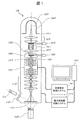
- FIG. 1 shows a schematic diagram of the overall configuration of the TEM 100.
- Each component of the TEM 100 is controlled by the electron microscope control system 117T as follows.
- the electron beam emitted from the electron source 103T at the top of the TEM mirror 101T is accelerated to an energy determined by the electron gun and the acceleration tube 102T.
- the convergence of the accelerated electron beam is adjusted by the front magnetic field of the converging lenses 104T and 107T and the objective lens 110T.
- the electron beam is deflected by the deflector 106T.
- the sample 109T held by the sample holder 108T is placed in the magnetic field of the objective lens 110T, which is a magnetic field electron lens, and the magnetic field up to the sample surface of the sample 109T is referred to as a “front magnetic field”. Is called “post-magnetic field”.
- the electron beam is guided to irradiate the observation region of the sample 109T as the irradiation electron beam 120T under conditions desired by the user such as brightness.
- the angle limit of the irradiation electron beam 120T is determined by the converging lens aperture device 105T.
- the electron beam 121T transmitted or scattered by the sample 109T is enlarged by the rear magnetic field of the objective lens 110T and the projection lens group 112T further downstream, and forms an enlarged image of the sample 109T on the fluorescent plate (projection surface) 115T.
- This image can be directly observed using the observation binoculars 113T and the like through the observation window 114T, and can further be recorded from below the projection surface by an imaging detector (CCD camera or the like) 116T or a two-dimensional imaging means such as a film.
- CCD camera CCD camera or the like
- the spherical aberration corrector 111T which has become widespread in recent years, is placed between the objective lens 110T and the projection lens group 112T in the TEM 100, and corrects on-axis aberrations up to the third order in addition to the spherical surface formed by the objective lens 110T. .
- the spherical aberration corrector 111T is controlled by the aberration correction control system 118T. This achieves a high resolution of less than 0.1 nm in the TEM100.
- FIG. 2 shows a schematic diagram of the overall configuration of the STEM 200. 2, the same components as those in FIG. 1 are denoted by the same reference numerals except “T”, and the description thereof is omitted unless particularly necessary.
- the STEM 200 includes an electron optical system that converges the electron beam emitted from the electron source 103 and scans the focused electron beam on the sample 109. Similar to the TEM, the electron beam emitted from the electron source 103 at the top of the STEM mirror 101 is guided to the electron gun and the acceleration tube 102 and the converging lenses 104 and 107 as the irradiation electron beam 120. The electron beam 120 is imaged so as to form a micro electron probe on the sample 109 by the front magnetic field of the objective lens 110.
- this micro electron probe is scanned two-dimensionally on the sample surface using a scan coil 127 (shown in FIGS. 12 and 13) disposed between the sample 109 and the aberration corrector 111. . Then, an electron beam transmitted or scattered at each point in the sample 109 is detected by an electron beam detector such as a bright field detector 126 and an annular dark field detector 125 downstream, and the intensity signal is acquired according to the raster scan. To do.
- a control device such as an electron microscope control system 117 or a control PC (Personal Computer) 119 forms an image of the sample 109 from an electron beam intensity signal from an electron beam detector. That is, the electron beam intensity signal is reconstructed into a two-dimensional image by the electron microscope control system 117 or the control PC 119. Thereby, for example, a two-dimensional image of the electron beam intensity, that is, a STEM image can be obtained on the screen of the control PC 119.
- the aberration corrector 111 is placed between the converging lens 107 and the objective lens 110, and removes the aberration in the objective lens 110 in advance (that is, cancels the aberration of the opposite sign equivalent to the objective lens aberration in advance). 111 is applied to the irradiation electron beam 120), and a finer electron probe free from blur due to aberration is imaged on the sample 109.
- the convergence angle of the irradiated electron beam on the sample surface is still limited by the converging lens aperture device 105.
- the projection lens group 112 downstream from the sample 109 is used to transmit the scattered or transmitted electron beams 121 and 122 to the detectors 125 and 126 under appropriate detection conditions.
- the imaging detector 116 is provided for aberration measurement or Ronchigram observation, but may be omitted if not required.
- FIG. 3 is a diagram for explaining a method for acquiring a diffractogram in a conventional TEM.
- FIG. 7 is a diagram for explaining a method for acquiring an image equivalent to a TEM diffractogram (hereinafter referred to as “STEM diffractogram”) in the STEM of this embodiment.
- STEM diffractogram TEM diffractogram
- the incident electron beam 120Ta irradiates the sample 109T in parallel with the front magnetic field 110Ta of the objective lens 110T.
- the sample 109T is a uniform amorphous thin film such as carbon, or a thin film mainly composed thereof.
- the carbon amorphous thin film has little absorption and can be regarded as a phase object with a good approximation, and since it has a random structure at the atomic level, the incident electrons are approximately isotropic. Scattered. Accordingly, a scattered electron beam 121Ta and a transmitted electron beam 122Ta that are uniform over a wide scattering angle range are generated downstream of the sample 109T. These are intermediately imaged on the intermediate image plane 150T by the back magnetic field 110Tb of the objective lens 110T. This intermediate image is further enlarged by the downstream projection lens group 112T (not shown in FIG. 3), and finally a TEM image is formed on the projection surface 115T (not shown in FIG. 3). The TEM image is observed using an imaging detector 116T or the like.
- And A ( ⁇ , z) are the electrostatic potential and vector potential of the sample, respectively.
- m, e, and h are the electron mass, charge, and Planck's constant, respectively.
- Equation 5 means taking along the electron trajectory passing through the sample and projecting it onto the exit surface. That is, the phase change of the formula 1 Can be said to directly represent the electromagnetic field information in the sample, and thus the structure.
- the electron wave function at the exit surface of the objective lens 110T is given by the Fourier transform of the equation (1). That is, It becomes.
- f 0 is the focal length of the objective lens
- F [] denotes the Fourier transform
- ⁇ ( ⁇ , ⁇ ) is an electron beam scattering angle. If the objective lens 110T and the projection lens group 112T form a complete image without lens aberration, the image can be obtained by inverse Fourier transform of the equation (8). Can be obtained.
- the objective lens 110T has an aberration, and the scattering angle is limited to a finite value. It becomes.
- a ( ⁇ ) is a transmission function determined by an objective aperture (not shown in FIG. 1)
- ⁇ ( ⁇ ) is an aberration function
- ⁇ is an electron beam wavelength.
- Equation (10) is that an extra phase change corresponding to the scattering angle is given to the electron beam due to the aberration, and as shown in FIG. 3, the ideal electron wavefront 130Ta includes an aberrational electron wavefront 130Tb. Will change. Equation (10) can be rewritten as follows based on the weak phase object approximation of the sample.
- an amorphous TEM image such as 500Ta shown in FIG. 5A is obtained on the projection surface 115T using the amorphous sample 109T shown in FIG.
- an amorphous TEM image such as 500Ta shown in FIG. 5A
- the above enhancement and suppression occur alternately as the scattering angle increases, so a ring-shaped (concentric) pattern (501Ta shown in FIG. 5B) that becomes a dark line at the scattering frequency at which the intensity is suppressed. Will get.
- An image obtained by Fourier transforming such a TEM image of an amorphous sample is called a “diffractogram”.
- the transmitted electron beam and the scattered electron beam are also correspondingly changed. It passes through another part of the objective lens 110T.
- the transmitted electron beam and the scattered electron beam are shifted at an angle ⁇ from 122Ta and 121Ta to 122Tb and 121Tb, respectively.
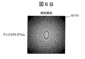
- a TEM image 600Tb shown in FIG. 6A is obtained.
- the frequency components included with different aberrations change while observing the same portion of the sample 109T.
- a TEM image 600Tb is obtained, and this is subjected to Fourier transform, whereby a diffractogram 601Tb shown in FIG. 6B is obtained.
- the diffractogram it is possible to know the local aberration (phase variation due to the position of the objective lens 110T through which the electron beam is transmitted), so that the diffract can be obtained at a plurality of electron beam incident angles.
- the phase variation ⁇ ( ⁇ ) due to the objective lens aberration by combining them.
- the least-order component of ⁇ ( ⁇ ) can be written as follows using the coefficients of defocus C 1 and two-fold astigmatism A 1 .
- ⁇ is a complex representation of angular space, It is. Also, Represents the conjugate complex value.
- the equation (14) By applying the equation (14) to the conditions of the equation (13) and analyzing the diffractograms 501Ta (FIG. 5B), 601Tb (FIG. 6B), etc., the defocus C 1 ( ⁇ ) and the electron beam incident angle ⁇
- the two-fold astigmatism A 1 ( ⁇ ) can be determined.
- ( ⁇ ) indicates an aberration determined at the incident angle ⁇ .
- C 1 ( ⁇ ) and A 1 ( ⁇ ) at the incident angle ⁇ are related to the axial aberration including the higher order as follows.
- This method can be extended to higher order aberration measurement in the same way. If the equation of Eq. 18 is supplemented so as to include the aberration of the desired order, the electron beam incident angle is changed as much as necessary to determine the aberration coefficient of the desired order, and the simultaneous equations of Eq.
- the axial aberration coefficient can be obtained as a solution of the linear simultaneous equations.
- the method of measuring aberrations by the above procedure is called the diffractogram tableau aberration measurement method, and is currently used as a standard method for measuring aberrations with high accuracy using the aberration correction TEM. Has been.
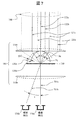
- FIG. 7 is a diagram for explaining an embodiment of the present invention, and is a diagram for explaining the principle that an aberration measuring method equivalent to the diffractogram tableau in the TEM explained in FIG. 3 can be applied in the STEM.
- the incident electron beam (bundle) 700 from above is converged mainly by the converging action of the front magnetic field 110a of the objective lens 110, and a micro electron probe is imaged on the sample 109.
- the micro electron probe is scanned on the sample 109 by using the scan coil (see FIGS. 12 and 13) to obtain the STEM image.
- both an electron beam transmitted through the sample 109 and an electron beam scattered by the sample 109 are taken into a detector and measured.
- the bright field detector 126a placed directly below the sample 109 and on the optical axis includes (i) an electron beam (irradiated electron beam 122a) perpendicularly incident on and transmitted through the sample 109, and (ii) a sample surface. From Incident at an angle of As a result, the scattered electron beam (irradiated electron beam 121a) vertically descending from the sample 109 reaches through the electron beam path 701a. These are signals for creating a bright field STEM image.
- the front magnetic field 110a of the objective lens 110 that contributes strongly in the formation of the STEM image as described above. If this has aberration as a lens, an extra phase variation due to the aberration is given to the electron beam when the electron beam passes, and the electron wavefront converging on the sample 109 is changed from the ideal wavefront 130a to the wavefront 130b including the variation due to the aberration. Deform. When this is applied to the bright field image observation conditions with the irradiation electron beam 122a and the irradiation electron beam 121a, each electron beam passes through a different part of the front magnetic field 110a of the objective lens 110 and thus converges on the sample 109.
- the irradiation electron beam 122a and the irradiation electron beam 121a are incident on the bright field detector 126a with different phase variations due to the aberration of the objective lens. This relationship is just the reverse of the relationship between electron beam irradiation and image formation described in TEM in FIG.
- the parallel incident electron beam is scattered by the sample 109T and passes through different positions of the back magnetic field 110Tb of the objective lens 110T together with the incident angle ⁇ of the electron beam and the scattered angle transmission electron beam.
- the phase variation due to the aberration is obtained, and an image is formed on the projection surface 115T.
- the electron beam incident in parallel is first converged by the front magnetic field 110a of the objective lens 110, it undergoes phase variation due to lens aberration.
- the electron beam scattered by the sample 109 and emitted in a specific direction is selectively detected by the bright field detector according to the position of the detector.
- an electron beam reaching one bright-field detector includes a scattered electron beam and a transmitted electron beam having a plurality of scattering angles ⁇ in the sample 109, and each of the electron beams is transmitted through an object transmitted in advance.
- Phase variation due to different lens aberrations depending on the location of the front magnetic field 110a of the lens 110 is received. Therefore, the enhancement and suppression of the electron beam intensity appear at a specific electron beam scattering angle due to the aberration of the objective lens 110, similar to that seen in the TEM.
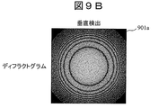
- the bright field image obtained by the bright field detector 126a obtains the STEM bright field image 900a of FIG. 9A in which a specific spatial frequency is suppressed.
- the suppressed spatial frequency can be confirmed as a dark concentric ring pattern in the image 901a of FIG. 9B obtained by Fourier transforming the STEM bright field image 900a as in TEM.
- this image 901a is an image equivalent to a diffractogram obtained by TEM, and is hereinafter referred to as a STEM diffractogram in this specification.
- the process of taking the diffractogram by changing the electron beam incident angle with TEM can be similarly performed by changing the selection of the electron beam emission angle ⁇ to be detected by changing the position of the detector.
- the transmitted electron beam incident on and transmitted through the sample 109 at the angle ⁇ when viewed with the bright field detector 126b at the position where the electron beam emitted from the sample 109 at the emission angle ⁇ in FIG. 7 is taken in, (i) the transmitted electron beam incident on and transmitted through the sample 109 at the angle ⁇ . (Irradiated electron beam 122b) and (ii) a scattered electron beam (irradiated electron beam 121b) incident on the sample 109 at an angle of ⁇ + ⁇ and turned back by ⁇ by scattering through the electron beam path 701b. It will reach the detector 126b.
- STEM bright field image 1000b (FIG. 10A) and STEM diffractogram 1001b (FIG. 10B) are obtained. Therefore, the angle of the electron beam emitted downward from the sample 109 is selected by means such as changing the position of the bright field detector.
- the axial aberration coefficient up to a desired order can be obtained even in the case of the STEM.
- FIG. 11 is a diagram in which a relationship between a sample and a detector for obtaining a bright field image used in the present invention is drawn by adding an electron beam.
- the electron beams 1101 and 1102 converged by the front magnetic field of the objective lens 110 have a half-angle cone shape and form a micro electron probe that scans the sample 109 at the tip.
- the electron beam 1111 transmitted through the sample 109 spreads at the same half angle ⁇ in the form of extending the cone of the incident electron beam below the sample 109.
- the electron beam 1112 scattered by the sample 109 is radiated into a cone inclined at a scattering angle ⁇ although it is still a half angle ⁇ .
- a scattering angle ⁇ for the sake of simplicity, only one scattered electron beam is drawn, but actually, a plurality of scatterings occur simultaneously according to the sample 109, and the cones of scattered electrons are inclined at the respective scattering angles accordingly. It will appear superimposed.
- substantially uniform scattering occurs in a wide angle range. Therefore, the cone-shaped electron beam 1112 shown in FIG. 11 is distributed almost continuously in the angular range.
- a bright field stop plate 1122 having a small hole 1121 for selection is disposed on the bright field detector 126. Is done. In the example of FIG. 11, there is a small hole 1121 in a region where the transmission electron beam and the scattered electron beam overlap on the bright field stop plate 1122, and only the transmission electron beam 1111b and the scattered electron beam 1112b that have passed therethrough are detected in the bright field. Reach vessel 126.
- the hole diameter of the small hole 1121 is determined according to the size of the structure to be observed. If the representative length of the sample structure to be observed is d, the half-angle ⁇ for viewing the small hole 1121 from the sample 109 is It becomes.
- ⁇ is the electron beam wavelength
- C s is the spherical aberration coefficient of the objective lens (110a in FIG. 7) in the optical system that performs aberration measurement.
- the hole diameter must be limited so that If the distance from the sample 109 to the bright field stop plate 1122, that is, the so-called camera length L, is 200 mm, the small hole diameter is 1.7 mm.
- the bright field detector 126 main body that detects the electron beam that has passed through the small hole 1121 of the bright field stop plate 1122 is a scintillator, a semiconductor detector, or the like for detecting electrons.
- the electron intensity signal detected by the bright field detector 126 is subjected to preprocessing such as amplification by the preamplifier 128 and is sent to the control PC 119.
- the control PC 119 performs STEM image formation and diffractogram calculation processing.
- the control PC 119 creates a plurality of images (FIG. 9B and FIG. 10B) by Fourier transforming each of the plurality of images acquired at a plurality of transmission angles with respect to the sample 109, and uses the plurality of images to transmit a plurality of transmissions.
- control PC119 obtains the aberration coefficients based on the defocus C 1 for each of a plurality of transmission angle (tau) and dyad symmetry astigmatism A 1 ( ⁇ ).
- the control PC 119 is a general-purpose computer.
- the process of the control PC 119 may be realized as a function of a program executed on the computer. That is, the process of the control PC 119 may be realized by storing a program code in a storage unit such as a memory and executing a program code by a processor such as a CPU (Central Processing Unit).
- a processor such as a CPU (Central Processing Unit).
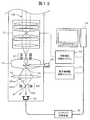
- FIG. 12 is a diagram showing the configuration of an embodiment of the present invention.
- a configuration example using a bright field detector array 1260 in which a plurality of bright field detectors 126a, 126b, and 126c are arranged in an array is shown.
- FIG. 12 shows a portion below the aberration corrector 111 of FIG. 2 for explaining the general structure of the STEM.
- the incident electron beam bundle 1200 is given a negative spherical aberration that cancels out the spherical aberration of the objective lens 110 in advance by the aberration corrector 111, and the micro electron probe is converged on the sample 109 by the front magnetic field of the objective lens 110.
- the electrons transmitted or scattered through the sample 109 are appropriately adjusted in magnification / camera length by the projection lens 112 and are incident on the lowermost bright field detector array 1260.
- FIG. 12 shows a bright field detector array 1260 including three bright field detectors 126a, 126b, and 126c.
- bright field images must be acquired at a plurality of emission angles corresponding to the number of aberrations to be measured.
- projection is performed so that the emission angle from the sample 109 to each bright field detector 126a, 126b, and 126c is appropriate.
- the lens 112 is adjusted.
- each of the bright field detectors 126a, 126b, and 126c can obtain an electron intensity signal at a different emission angle.
- reference numerals 1201 a, 1201 b, and 1201 c in FIG. 12 indicate three transmission and scattered electron beam paths emitted from the sample 109.
- Signals obtained by the bright field detectors 126a, 126b, and 126c are amplified by the preamplifiers 128a, 128b, and 128c, and sent to the control PC 119.
- the control PC 119 can simultaneously obtain a bright field image, and thus a diffractogram, from the signals obtained by the bright field detectors 126a, 126b, and 126c.
- FIG. 12 only three detectors are shown for the sake of simplification, but if nine or more detectors are arranged two-dimensionally, the fifth-order or lower axial aberration can be calculated. . That is, according to the embodiment shown in FIG. 12, a plurality of electron beam incidence conditions can be changed while the electron beam incidence conditions are changed, such as the diffractogram tableau method in the original TEM and the probe measurement method conventionally used in the STEM. There is no need to repeat the measurement. Further, the extraction of aberration information from the obtained STEM image and the calculation of the on-axis aberration can be performed with high accuracy by the same method as the diffractogram tableau method in TEM that has been sufficiently confirmed so far.
- FIG. 13 is a diagram showing the configuration of another embodiment of the present invention.
- this embodiment includes one bright field detector 126 and an electron beam deflector 129 for guiding the transmitted or scattered electron beam to the bright field detector 126 for selection.
- the electron beam deflector 129 sequentially selects electron beams having different emission angles, and acquires STEM images for the different emission angles.
- FIG. 13 for the sake of simplicity, three transmitted and scattered electron beams (electron beam paths) 1201a, 1201b, and 1201c emitted from the sample 109 are shown.
- the electron beam deflector 129 is used first.
- One transmitted and scattered electron beam 1201a is guided to the bright field detector 126, and an STEM image corresponding to the emission angle is obtained.
- the electron beam is shaken again so that the second transmitted and scattered electron beam 1201b is again guided to the bright field detector 126, and an STEM image is acquired.
- STEM images are acquired in the same manner for the third transmitted and scattered electron beam 1201c.
- the transmitted and scattered electron beams 1201a, 1201b, and 1201c detected by the electron beam deflector 129 are sequentially selected, and a necessary number of STEM images are acquired. After acquiring the STEM image, the axial aberration coefficient is calculated by the method described above.
- the electron beam to be detected can be selected by adjusting only the electron beam deflector 129 directly above the bright field detector 126 without adjusting the electron optical element such as a detector. That is, it is possible to adjust only the electron beam deflector 129 directly above the bright field detector 126 and acquire a STEM image necessary for measurement.
- the incident electron beam is transmitted using at least two stages of deflectors that place a TEM image or STEM image necessary for measurement above the corrector.
- the electron beam incident angle with respect to the sample must be adjusted with accurate parallel displacement. Therefore, according to the embodiment shown in FIGS. 12 and 13, it is easy to extract aberration information as compared with the existing aberration measurement method, and it is possible to provide an aberration measurement method with high measurement accuracy.
- FIGS. 14A to 14C show examples of the bright field detector array 1260 used in the example of FIG.
- the bright field detector array 1260 used in the aberration measurement method of this embodiment includes the electron detector body and the limit of the electron beam angle to be detected according to the condition of the equation (20). And a diaphragm for carrying out above.
- each of the single hole apertures 1402a, 1402b, 1402c,... Has a hole for limiting the electron beam to an emission angle that is a detection target. Note that the diaphragm need only be capable of limiting the emission angle of the electron beam that is appropriately detected by each of the electron detectors 1401a, 1401b, 1401c,. .
- the bright field detector array 1260B of FIG. 14B includes a plurality of electron detectors 1401a, 1401b, 1401c,..., And a single diaphragm plate 1402.
- the diaphragm plate 1402 has a porous array corresponding to the detector array. Therefore, the bright field detector array 1260B can be configured by inserting the diaphragm plate 1402 on the plurality of electron detectors 1401a, 1401b, 1401c,.
- the diaphragm plate 1402 may be of a mechanism that is inserted later onto the detector array independently of the electron detectors 1401a, 1401b, 1401c,.
- the bright field detector array 1260C of FIG. 14C includes a diaphragm plate 1402, a conversion element 1404, and a two-dimensional imaging sensor 1405.
- a two-dimensional imaging sensor 1405 such as a CCD may be substituted for the detector side.
- an electron beam that has passed through a diaphragm plate 1402 having a porous array of an appropriate arrangement is guided to a two-dimensional imaging sensor 1405 through a conversion element 1404 (in the case of a CCD, from an electron such as a fluorescent plate or a scintillator to light). Conversion element 1404 is used).
- a signal of the pixel of the two-dimensional imaging sensor 1405 corresponding to each hole of the diaphragm plate 1402 is taken out, and a scanning image (STEM image) may be reproduced for each electron beam.
- STEM image scanning image
- FIGS. 15A to 15B show examples of arrangements of electron detectors and apertures in a bright field detector array.
- the number of bright-field detectors may be sufficient to satisfy the simultaneous equations (Equation 18) sufficient to calculate the desired axial aberration coefficient, and the arrangement also calculates the desired axial aberration coefficient. It suffices if it is at a position where an appropriate emission angle can be selected. Note that the selection of the emission angle can also be adjusted as appropriate with the projection lens 112 shown in FIGS.
- an axial aberration coefficient can be obtained in principle.
- FIG. 16A is a flowchart of an aberration corrector adjustment operation using the aberration measurement method according to one embodiment of the present invention.
- the lens excitation and deflector optical conditions that can be determined by prior experiments and simulations are set as preset conditions (1601).
- step 1602 adjustment for obtaining a bright field image is performed (1602).
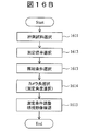
- the contents of step 1602 will be described with reference to FIG. 16B.
- a measurement sample is selected and a measurement location in the sample is selected (1611).
- STEM magnification and irradiation conditions suitable for aberration measurement are set (1612, 1613). The magnification is appropriately adjusted according to the magnitude of the remaining aberration.
- the effective camera length from the sample 109 to the bright field detector is adjusted by adjusting the projection lens 112 (1614). In this operation, particularly when the bright field detector array 1260 is used, the camera length is set so that an electron beam having an appropriate emission angle reaches each detector of the array.
- respective setting values and STEM images are displayed on the monitor of the control PC 119 (1615).
- the operator can adjust various setting conditions via the user interface.
- the STEM diffractogram is acquired (1603).
- the contents of step 1603 will be described with reference to FIG. 16C.
- this process will be described using the bright field detector array 1260 of FIG.
- the bright field detector array 1260 is activated (1621).
- a diaphragm such as a diaphragm plate 1402 in FIG. 14B
- an imaging operation two-dimensional scanning on the sample surface with an electronic probe
- STEM images in the electron beam emission azimuth from the sample 109 corresponding to the respective detectors can be obtained from the signals obtained by the respective detectors of the bright field detector array 1260. This satisfies the requirement based on the measurement principle described in FIG. If each STEM image obtained here is Fourier-transformed (1624) and matched with the electron beam emission angle from the sample 109, the STEM diffractogram table can be obtained (1625).
- the STEM diffractogram table means a table in which the electron beam emission angle from the sample 109 is associated with the STEM diffractogram.
- the control PC 119 calculates an axial aberration coefficient using the STEM diffractogram table obtained in step 1603 (1604). This step is almost the same as the procedure for calculating the on-axis aberration coefficient from the diffractogram tableau in the TEM as described above. Details will be described with reference to FIG. 16D. First, a defocus C 1 ( ⁇ i ) and a two-fold symmetric astigmatism A 1 ( ⁇ i ) with respect to the output angle ⁇ i corresponding to the i-th among a plurality of obtained diffractograms are extracted (1631).
- a multiple simultaneous equation is created from the relational expression of C 1 ( ⁇ i ) and A 1 ( ⁇ i ) and the axial aberration coefficient shown in the equation (18), and means such as the least square method is used.
- the axial aberration coefficient is derived (1632).
- the axial aberration count to be corrected is output (1633), and displayed on the monitor of the control PC 119 by graphical means such as an aberration coefficient, aberration figure, or wavefront aberration (1634).
- the operator can confirm the information displayed on the monitor.
- the STEM diffractogram table is also displayed on the monitor at the same time (1635). Displaying the STEM diffractogram table is useful for grasping the aberration state, and allows the operator to confirm the appropriateness of the aberration measurement regarding what diffractogram was acquired and the aberration measurement was performed. So desirable.
- the control PC 119 determines the correction state from the aberration coefficient obtained through a series of aberration measurements (1605). If the measured value of the aberration coefficient to be corrected is equal to or less than a separately determined tolerance, this aberration adjustment is complete. On the other hand, if the aberration coefficient deviates from the allowable value, residual aberration compensation adjustment is performed to reduce the aberration (1606). Then, in order to confirm whether or not the aberration is sufficiently reduced by the correction performed according to the compensation adjustment, and whether or not another aberration is increased parasitically at the time of tuning, the process returns to step 1602. Repeat the aberration measurement. As the aberration correction progresses and the residual aberration decreases, the appropriate image magnification and camera length also change, so it is better to adjust them appropriately.
- step 1605 After obtaining a diffractogram (1603) and calculating an aberration coefficient (1604), it is determined in step 1605 that all the aberration coefficients to be compensated are equal to or less than an allowable value and the aberration correction adjustment is completed. Until this, the aberration measurement and compensation adjustment steps as described above are repeated. As described above, the aberration states of the STEM aberration corrector 111 and the objective lens 110 can be evaluated.
- aberration measurement is important for evaluating the state of the charged particle optical system.
- a highly accurate aberration (coefficient) measurement technique has been required more than ever before for adjustment of the aberration corrector and evaluation of the aberration correction state.
- these aberration measurement methods there are known an aberration graphic method and a probe tableau method for acquiring aberration-induced displacement and image distortion by changing a plurality of incident conditions of a charged particle beam to a lens to be measured, and deriving an aberration coefficient.
- the measurement procedure is complicated and the measurement time is long. This made it difficult to adjust the aberration corrector itself, which requires repeated measurement.
- STEM aberration measurement an image (STEM diffractogram) equivalent to a diffractogram using the reciprocity of STEM and TEM is acquired, and an axial aberration coefficient is calculated using this. This avoids complex image analysis for aberration information extraction found in the Ronchigram method.
- a bright field detector array 1260 in which a plurality of STEM bright field detectors are arranged, or a detector equivalent thereto is used. Accordingly, STEM images for a plurality of incident angles can be obtained simultaneously in parallel, and a STEM diffractogram for each incident angle can be calculated. Therefore, information equivalent to the diffractogram can be acquired collectively without repeating a plurality of measurements. In other words, the aberration measurement can be completed in a short time in a single measurement. Therefore, the complexity of measurement can be greatly reduced.
- a plurality of transmission and scattering electron beams having different angles are sequentially selected by the electron beam deflector 129, and the transmission and scattered electron beams are detected by one STEM bright field detector 126.
- this configuration it is possible to adjust only the electron beam deflector 129 directly above the bright field detector 126 and obtain a STEM image necessary for measurement.
- This configuration is simpler than the conventional aberration measurement using the diffractogram tableau method with the TEM or the probe tableau method with the STEM, and the complexity of the measurement can be reduced.
- this invention is not limited to the Example mentioned above, Various modifications are included.
- the above-described embodiments have been described in detail for easy understanding of the present invention, and are not necessarily limited to those having all the configurations described.
- a part of the configuration of one embodiment may be replaced with the configuration of another embodiment, and the configuration of another embodiment may be added to the configuration of one embodiment.
- control devices such as the aberration correction control system (118T, 118), the electron microscope control system (117T, 117), and the control PC (119T, 119) of the embodiment are partly or entirely designed by, for example, an integrated circuit. This may be realized by hardware.
- the functions of the control device described above may be realized by software program codes.
- a non-transitory computer readable medium non-transitory computer readable medium in which the program code is recorded is provided to the information processing device (computer), and the information processing device (or CPU) is a non-transitory computer readable medium.
- the program code stored in is read.
- non-transitory computer-readable medium for example, a flexible disk, a CD-ROM, a DVD-ROM, a hard disk, an optical disk, a magneto-optical disk, a CD-R, a magnetic tape, a nonvolatile memory card, a ROM, and the like are used.
- the program code may be supplied to the information processing apparatus by various types of temporary computer-readable media.
- Examples of transitory computer readable media include electrical signals, optical signals, and electromagnetic waves.
- the temporary computer-readable medium can supply the program to the information processing apparatus via a wired communication path such as an electric wire and an optical fiber, or a wireless communication path.
- control lines and information lines in the drawings indicate what is considered necessary for the explanation, and not all control lines and information lines on the product are necessarily shown. All the components may be connected to each other.
- TEM 200 STEM 101, 101T: Mirror body 102, 102T: Electron gun and acceleration tube 103, 103T: Electron source 104, 104T: Converging lens 105, 105T: Converging lens diaphragm 106, 106T: Deflectors 107, 107T: Converging lenses 108, 108T : Sample holder 109, 109T: Sample 110, 110T: Objective lens 110a, 110Ta: Objective lens pre-magnetic field 110b, 110Tb: Objective lens post-magnetic field 111, 111T: Aberration corrector 112, 112T: Projection lens 113T: Observation binoculars 114T: Observation window 115T: Projection surface (fluorescent screen) 116, 116T: Imaging detector (CCD camera, etc.) 117, 117T: Electron microscope control system 118, 118T: Aberration correction control system 119, 119T: Control PC 120, 120T: irradiation electron
Landscapes
- Chemical & Material Sciences (AREA)
- Analytical Chemistry (AREA)
- Engineering & Computer Science (AREA)
- Computer Vision & Pattern Recognition (AREA)
- Analysing Materials By The Use Of Radiation (AREA)
Abstract
La présente invention concerne un dispositif à faisceau de particules chargées au moyen duquel on peut facilement comparer l'extraction d'informations d'aberration à des procédés de mesure d'aberration existants, et pouvant exécuter une mesure extrêmement précise d'aberration. Le dispositif à faisceau de particules chargées comprend les composants suivants : un système optique électronique qui balaie des faisceaux de particules chargées ayant fait l'objet d'une convergence sur un échantillon (109); des systèmes de détection (126a, 126b) qui détectent des faisceaux de particules chargées qui sont passés à travers l'échantillon (109) ou qui ont été diffusés à partir de ce dernier; un dispositif de correction d'aberration qui corrige une aberration du système optique électronique; et un dispositif de commande qui forme une image de l'échantillon (109) à partir de signaux provenant des systèmes de détection (126a, 126b). Dans le dispositif à faisceau de particules chargées, plusieurs images sont formées par application d'une transformation de Fourier à chacune des plusieurs images de l'échantillon (109) ayant fait l'objet d'une acquisition à plusieurs angles de détection, et des informations d'aberration sont trouvées pour chacun des plusieurs angles de détection au moyen des plusieurs images.
Applications Claiming Priority (2)
| Application Number | Priority Date | Filing Date | Title |
|---|---|---|---|
| JP2013159518A JP2015032384A (ja) | 2013-07-31 | 2013-07-31 | 荷電粒子線装置及び荷電粒子線装置における収差測定法 |
| JP2013-159518 | 2013-07-31 |
Publications (1)
| Publication Number | Publication Date |
|---|---|
| WO2015015985A1 true WO2015015985A1 (fr) | 2015-02-05 |
Family
ID=52431526
Family Applications (1)
| Application Number | Title | Priority Date | Filing Date |
|---|---|---|---|
| PCT/JP2014/067493 Ceased WO2015015985A1 (fr) | 2013-07-31 | 2014-07-01 | Dispositif à faisceau de particules chargées et procédé de mesure d'aberration dans un dispositif à faisceau de particules chargées |
Country Status (2)
| Country | Link |
|---|---|
| JP (1) | JP2015032384A (fr) |
| WO (1) | WO2015015985A1 (fr) |
Cited By (2)
| Publication number | Priority date | Publication date | Assignee | Title |
|---|---|---|---|---|
| TWI792070B (zh) * | 2019-10-22 | 2023-02-11 | 荷蘭商Asml荷蘭公司 | 判定帶電粒子束工具所獲得之影像中之像差的方法、判定帶電粒子束工具之設置的方法、及帶電粒子束工具 |
| EP4254467A1 (fr) * | 2022-03-29 | 2023-10-04 | Jeol Ltd. | Microscope électronique et procédé de mesure d'aberration |
Families Citing this family (7)
| Publication number | Priority date | Publication date | Assignee | Title |
|---|---|---|---|---|
| JP6533665B2 (ja) * | 2015-02-03 | 2019-06-19 | 日本電子株式会社 | 電子顕微鏡および収差測定方法 |
| JP6464064B2 (ja) * | 2015-09-07 | 2019-02-06 | 日本電子株式会社 | 荷電粒子装置 |
| JP6647854B2 (ja) * | 2015-12-22 | 2020-02-14 | 日本電子株式会社 | 収差補正方法および荷電粒子線装置 |
| JP6677519B2 (ja) * | 2016-02-03 | 2020-04-08 | 日本電子株式会社 | 電子顕微鏡および収差測定方法 |
| JP6770482B2 (ja) * | 2017-05-22 | 2020-10-14 | 日本電子株式会社 | 荷電粒子線装置および走査像の歪み補正方法 |
| KR102490174B1 (ko) * | 2020-11-25 | 2023-01-19 | 한국기초과학지원연구원 | 전자현미경의 수차 값을 예측하기 위한 장치 및 그 동작 방법 |
| WO2024262601A1 (fr) * | 2023-06-21 | 2024-12-26 | 国立大学法人東京大学 | Procédé de mesure utilisant un microscope électronique à transmission et à balayage, système de microscope électronique à transmission et à balayage, et programme |
Citations (2)
| Publication number | Priority date | Publication date | Assignee | Title |
|---|---|---|---|---|
| JPH07220669A (ja) * | 1994-01-31 | 1995-08-18 | Jeol Ltd | 非点・入射軸補正装置を備えた電子顕微鏡 |
| JP2013089599A (ja) * | 2011-10-19 | 2013-05-13 | Fei Co | 収差補正器を備えたstemの調整方法 |
-
2013
- 2013-07-31 JP JP2013159518A patent/JP2015032384A/ja active Pending
-
2014
- 2014-07-01 WO PCT/JP2014/067493 patent/WO2015015985A1/fr not_active Ceased
Patent Citations (2)
| Publication number | Priority date | Publication date | Assignee | Title |
|---|---|---|---|---|
| JPH07220669A (ja) * | 1994-01-31 | 1995-08-18 | Jeol Ltd | 非点・入射軸補正装置を備えた電子顕微鏡 |
| JP2013089599A (ja) * | 2011-10-19 | 2013-05-13 | Fei Co | 収差補正器を備えたstemの調整方法 |
Cited By (5)
| Publication number | Priority date | Publication date | Assignee | Title |
|---|---|---|---|---|
| TWI792070B (zh) * | 2019-10-22 | 2023-02-11 | 荷蘭商Asml荷蘭公司 | 判定帶電粒子束工具所獲得之影像中之像差的方法、判定帶電粒子束工具之設置的方法、及帶電粒子束工具 |
| US12183540B2 (en) | 2019-10-22 | 2024-12-31 | Asml Netherlands B.V. | Systems and methods of determining aberrations in images obtained by a charged-particle beam tool |
| EP4254467A1 (fr) * | 2022-03-29 | 2023-10-04 | Jeol Ltd. | Microscope électronique et procédé de mesure d'aberration |
| JP2023146461A (ja) * | 2022-03-29 | 2023-10-12 | 日本電子株式会社 | 電子顕微鏡および収差測定方法 |
| JP7498212B2 (ja) | 2022-03-29 | 2024-06-11 | 日本電子株式会社 | 電子顕微鏡および収差測定方法 |
Also Published As
| Publication number | Publication date |
|---|---|
| JP2015032384A (ja) | 2015-02-16 |
Similar Documents
| Publication | Publication Date | Title |
|---|---|---|
| WO2015015985A1 (fr) | Dispositif à faisceau de particules chargées et procédé de mesure d'aberration dans un dispositif à faisceau de particules chargées | |
| JP3867524B2 (ja) | 電子線を用いた観察装置及び観察方法 | |
| US6552340B1 (en) | Autoadjusting charged-particle probe-forming apparatus | |
| JP5103532B2 (ja) | 収差補正器を備えた荷電粒子線装置 | |
| EP2091063B1 (fr) | Dispositif d'observation de faisceau à électrons utilisant un champ magnétique pré-spécimen en tant que lentille de formation d'image et procédé d'observation de spécimen | |
| EP2639814B1 (fr) | Équipement optique à particules chargées et procédé de mesure d'aberration de lentille | |
| JP5603421B2 (ja) | 自動収差補正法を備えた荷電粒子線装置 | |
| JP5727564B2 (ja) | 荷電粒子レンズ系における収差を調査及び補正する方法 | |
| JP4790567B2 (ja) | ロンチグラムを用いた収差測定方法及び収差補正方法及び電子顕微鏡 | |
| JP2007179753A (ja) | 走査透過電子顕微鏡、及び収差測定方法 | |
| CN1979751B (zh) | 用于确定粒子-光学透镜的像差函数的像差系数的方法 | |
| JP2006173027A (ja) | 走査透過電子顕微鏡、及び収差測定方法、ならびに収差補正方法 | |
| JP6163063B2 (ja) | 走査透過電子顕微鏡及びその収差測定方法 | |
| JP5817360B2 (ja) | 走査透過型電子顕微鏡の観察方法及び走査透過型電子顕微鏡 | |
| JP4337832B2 (ja) | 電子線を用いた観察装置及び観察方法 | |
| EP3637452A1 (fr) | Microscope à particules chargées et procédé de réglage d'un microscope à particules chargées | |
| JP5777984B2 (ja) | 多極子測定装置 | |
| JP7285871B2 (ja) | 走査透過電子顕微鏡および光学系の調整方法 | |
| JP4431624B2 (ja) | 荷電粒子線調整方法、及び荷電粒子線装置 | |
| EP1883094A1 (fr) | Appareil à faisceau de particules et procédé pour l'examen d'un échantillon | |
| JP2010016007A (ja) | 荷電粒子線調整方法及び荷電粒子線装置 | |
| TW202605880A (zh) | 帶電粒子線裝置及像差計測方法 | |
| JP2018195546A (ja) | 荷電粒子線装置 |
Legal Events
| Date | Code | Title | Description |
|---|---|---|---|
| 121 | Ep: the epo has been informed by wipo that ep was designated in this application |
Ref document number: 14831769 Country of ref document: EP Kind code of ref document: A1 |
|
| NENP | Non-entry into the national phase |
Ref country code: DE |
|
| 122 | Ep: pct application non-entry in european phase |
Ref document number: 14831769 Country of ref document: EP Kind code of ref document: A1 |