WO2015037266A1 - 過充電保護装置 - Google Patents
過充電保護装置 Download PDFInfo
- Publication number
- WO2015037266A1 WO2015037266A1 PCT/JP2014/060749 JP2014060749W WO2015037266A1 WO 2015037266 A1 WO2015037266 A1 WO 2015037266A1 JP 2014060749 W JP2014060749 W JP 2014060749W WO 2015037266 A1 WO2015037266 A1 WO 2015037266A1
- Authority
- WO
- WIPO (PCT)
- Prior art keywords
- overcharge protection
- voltage
- storage battery
- fet
- protection device
- Prior art date
- Legal status (The legal status is an assumption and is not a legal conclusion. Google has not performed a legal analysis and makes no representation as to the accuracy of the status listed.)
- Ceased
Links
Images


Classifications
-
- H—ELECTRICITY
- H02—GENERATION; CONVERSION OR DISTRIBUTION OF ELECTRIC POWER
- H02J—ELECTRIC POWER NETWORKS; CIRCUIT ARRANGEMENTS OR SYSTEMS FOR SUPPLYING OR DISTRIBUTING ELECTRIC POWER; SYSTEMS FOR STORING ELECTRIC ENERGY
- H02J7/00—Circuit arrangements for charging or discharging batteries or for supplying loads from batteries
- H02J7/60—Circuit arrangements for charging or discharging batteries or for supplying loads from batteries including safety or protection arrangements
- H02J7/61—Circuit arrangements for charging or discharging batteries or for supplying loads from batteries including safety or protection arrangements against overcharge
-
- H—ELECTRICITY
- H02—GENERATION; CONVERSION OR DISTRIBUTION OF ELECTRIC POWER
- H02J—ELECTRIC POWER NETWORKS; CIRCUIT ARRANGEMENTS OR SYSTEMS FOR SUPPLYING OR DISTRIBUTING ELECTRIC POWER; SYSTEMS FOR STORING ELECTRIC ENERGY
- H02J7/00—Circuit arrangements for charging or discharging batteries or for supplying loads from batteries
- H02J7/90—Regulation of charging or discharging current or voltage
- H02J7/96—Regulation of charging or discharging current or voltage in response to battery voltage
- H02J7/963—Regulation of charging or discharging current or voltage in response to battery voltage in response to battery voltage gradient
Definitions
- Embodiments of the present invention relate to an overcharge protection device.
- a fuse with a heater called a fusing resistor is used, and the connection between the storage battery and the main circuit is cut off by energizing the heater and blowing the fuse.
- the overcharge protection device of the embodiment includes a switch unit and a control unit.
- the switch unit connects a plurality of switch elements connected in series to a fuse and a storage battery connected in parallel between the storage battery and a charging unit that charges the storage battery.
- the control unit detects the output voltage of the storage battery and, when the detected output voltage exceeds a predetermined overcharge detection voltage, turns on the plurality of switch elements to short-circuit between the positive electrode terminal and the negative electrode terminal of the storage battery. .
- FIG. 1 is a diagram illustrating a configuration of the storage battery device according to the first embodiment.
- FIG. 2 is a diagram illustrating a specific configuration of the overcharge protection device included in the storage battery device according to the first embodiment.
- FIG. 3 is a flowchart showing a flow of failure detection processing of the overcharge protection FET by the overcharge protection device according to the first embodiment.
- FIG. 4 is a diagram illustrating a specific configuration of the overcharge protection device included in the storage battery device according to the second embodiment.
- FIG. 5 is a diagram illustrating an example of a wiring board included in the overcharge protection device according to the third embodiment.
- FIG. 6 is a diagram illustrating a configuration of a storage battery device according to a modification.
- FIG. 1 is a diagram illustrating a configuration of the storage battery device according to the first embodiment.
- the storage battery device 1 includes a battery module 101, a shunt resistor 103, a charge control FET (Field Effect Transistor) 104, a discharge control FET 105, a fuse F, and a positive main circuit.
- a terminal TP, a negative main circuit terminal TM, an overcharge protection device 100, and a power supply circuit 120 are provided.
- the storage battery device 1 is connected to a storage battery utilization device 117 (an example of a charging unit) that charges and discharges the battery module 101.
- the positive main circuit terminal TP is connected to the positive terminal (positive main circuit) of the storage battery utilization device 117.
- the negative electrode main circuit terminal TM is connected to the negative side terminal (negative side main circuit) of the storage battery utilization device 117.
- the storage battery utilization device 117 is connected to a battery management device 107 described later via a communication line 115.
- the power circuit 120 supplies power from the battery module 101 or the storage battery utilization device 117 to the entire storage battery device 1.
- the battery module 101 (an example of a storage battery), a plurality of battery cells 101a (for example, secondary batteries such as a lithium ion battery and a lead storage battery) are connected in series. And the battery module 101 supplies electric power to the storage battery utilization apparatus 117 connected via the positive electrode main circuit terminal TP and the negative electrode main circuit terminal TM which are mentioned later.
- battery cells 101a for example, secondary batteries such as a lithium ion battery and a lead storage battery
- the positive electrode main circuit terminal TP is connected to the high potential side of the battery module 101 and is a terminal for supplying power from the battery module 101 to the storage battery utilization device 117.
- the negative electrode main circuit terminal TM is a terminal that is connected to the low potential side of the battery module 101 and supplies power from the battery module 101 to the storage battery utilization device 117.
- the fuse F is connected between the battery module 101 and the storage battery utilization device 117.
- the fuse F is connected to the high potential side of the battery module 101.
- the fuse F cuts off the connection between the battery module 101 and the storage battery utilization device 117 when an overcurrent flows from the battery module 101 to the storage battery utilization device 117 or when an overcharge state occurs in the battery module 101.
- the shunt resistor 103 is used to detect the amount of current flowing through the battery module 101.
- the shunt resistor 103 is connected to the low potential side of the battery module 101.
- the charge control FET 104 is composed of an NMOS (Negative channel Metal Oxide Semiconductor) -FET, and is connected between the battery module 101 and the storage battery using device 117.
- the charge control FET 104 is connected in parallel with a rectifying diode (not shown) that flows current when power is supplied from the battery module 101 to the storage battery utilization device 117.
- the discharge control FET 105 is composed of an NMOS-FET and is connected between the battery module 101 and the storage battery utilization device 117.
- the discharge control FET 105 is connected in parallel with a rectifying diode (not shown) that flows current when the battery module 101 is charged with the power supplied from the storage battery utilization device 117.
- the charge control FET 104 and the discharge control FET 105 are configured by NMOS-FETs, but may be configured by PMOS (Positive channel Metal Oxide Semiconductor) -FETs or IGBTs (Insulated Gate Bipolar Transistors).
- bipolar transistors can be used as the charge control FET 104 and the discharge control FET 105. When bipolar transistors are used as the charge control FET 104 and the discharge control FET 105, it is necessary to provide a current control circuit for controlling on / off of the bipolar transistor by flowing a current through the base of the bipolar transistor.
- the overcharge protection device 100 is a device that interrupts the current flowing from the storage battery utilization device 117 to the battery module 101 when the battery module 101 is charged.
- the overcharge protection device 100 includes a wiring board HR, a switch unit 102, a battery management circuit 107, and a high side (high potential side) drive circuit 109.
- the switch unit 102 has two overcharge protection FETs 106 and 108 (an example of a plurality of switch elements) connected in series connected in parallel to the battery module 101 and the fuse F.
- the overcharge protection FETs 106 and 108 are formed of NMOS-FETs, but the present invention is not limited to this, and for example, PMOS-FETs or IGBTs may be used.
- bipolar transistors can be used as the overcharge protection FETs 106 and 108. When a bipolar transistor is used as the overcharge protection FETs 106 and 108, it is necessary to provide a current control circuit for controlling on and off of the bipolar transistor by flowing a current through the base of the bipolar transistor.
- the switch unit 102 includes two overcharge protection FETs 106 and 108, but may have a plurality of switch elements connected in series. For example, the switch unit 102 is connected in series. You may have three or more switch elements.
- the wiring board HR has a current limiting resistor formed by a wiring pattern connected in series to the overcharge protection FETs 106 and 108 included in the switch unit 102.
- the current limiting resistor is configured by the wiring pattern of the wiring board HR.
- the present invention is not limited to this, and a resistive element may be used as the current limiting resistor.
- the high-side drive circuit 109 has two overcharge protections according to a power supply voltage V1 applied by the control power supply G via a terminal T1 (see FIG. 2) and a high-side FET drive signal input from a battery management circuit 107 described later.
- the overcharge protection FET 106 connected to the high potential side of the battery module 101 among the FETs 106 and 108 is controlled.
- the battery management circuit 107 is connected to a storage battery utilization device 117 that controls the entire storage battery device 1 via a communication line 115, and performs charging / discharging of the battery module 101, interruption of current flowing through the battery module 101 when the battery module 101 is charged, and the like. Control. Specifically, the battery management circuit 107 uses the voltage detection lines 114 connected to the low potential side and the high potential side of each of the plurality of battery cells 101a included in the battery module 101 to each of the plurality of battery cells 101a. An output voltage (hereinafter referred to as a cell voltage) is detected. Then, the battery management circuit 107 controls charging and discharging of the battery module 101 based on the detected cell voltage.
- the battery management circuit 107 when the battery management circuit 107 receives a power supply instruction from the battery module 101 for instructing power supply from the battery module 101 to the storage battery utilization device 117, the battery management circuit 107 discharges the battery module 101 in accordance with the power supply instruction. Is output to the discharge control FET 105. Further, the battery management circuit 107 outputs a charge control FET drive signal for instructing charging of the battery module 101 to the charge control FET 104 based on the detection result of the cell voltage of each of the plurality of battery cells 101a.
- the battery management circuit 107 also provides a high-side (high-potential side) FET drive signal to the high-side drive circuit 109 when the cell voltage detected when the battery module 101 is charged exceeds a predetermined overcharge detection voltage. Is output to turn on the overcharge protection FET 106 connected to the high potential side of the battery module 101, and the low side (low potential side) is connected to the gate of the overcharge protection FET 108 connected to the low potential side of the battery module 101. An FET drive signal is output to turn on the overcharge protection FET 108.
- the battery management circuit 107 (an example of a control unit) cannot stop the charging current by the charge control FET drive signal from the battery management circuit 107 due to a short circuit failure of the charge control FET 104 when the battery module 101 is charged,
- the cell voltage of the battery module 101 exceeds a predetermined overcharge detection voltage, between the positive terminal BP that is a terminal on the high potential side of the battery module 101 and the negative terminal BM that is a terminal on the low potential side of the battery module 101
- the fuse F is blown by the short-circuit current of the battery module 101. Therefore, according to the present embodiment, when an overcharged state of the battery module 101 occurs when the battery module 101 is charged, the battery module is obtained by fusing the fuse F without providing a heater or the like for fusing the fuse F. 101 can be protected.
- the plurality of overcharge protection FETs 106 and 108 connected in series are short-circuited between the positive terminal BP and the negative terminal BM of the battery module 101. , 108 even if a short circuit failure occurs, the positive terminal BP and the negative terminal BM of the battery module 101 are not short-circuited. Therefore, any one of the plurality of overcharge protection FETs 106, 108 is short-circuited. It is possible to prevent the fuse F from being blown by mistake due to a failure.
- the battery management circuit 107 turns on the overcharge protection FETs 106 and 108 after the predetermined time has elapsed after turning on.
- the charge protection FETs 106 and 108 may be turned off.
- the overcharge protection FETs 106 and 108 and the wiring board HR are caused by a short-circuit current that flows to blow the fuse F flowing through the overcharge protection FETs 106 and 108 for a long time. Can prevent breakage.
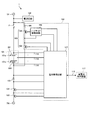
- FIG. 2 is a diagram illustrating a specific configuration of the overcharge protection device included in the storage battery device according to the first embodiment.
- the overcharge protection device 100 has two systems of switch units 102 as shown in FIG.
- Each switch unit 102 includes two overcharge protection FETs 106 and 108 connected in series between a terminal TF connected to the fuse F and a ground terminal GND connected to the negative terminal BM of the battery module 101.
- the switch unit 102 includes a rectifying diode D1 that is connected in parallel to each of the two overcharge protection FETs 106 and 108 and allows a current to flow when the battery module 101 is charged.
- the switch unit 102 is connected between the gate and the source of each of the overcharge protection FETs 106 and 108, and is used for stabilizing the operation for stabilizing the potential difference between the gate and the source of each of the overcharge protection FETs 106 and 108. It has a pull-down resistor R1.
- the overcharge protection device 100 has two systems of the switch unit 102, but it is only necessary to have at least one switch unit 102.
- the overcharge protection device 100 includes a wiring board HR connected in series to two overcharge protection FETs 106 and 108 between a terminal TF and a ground terminal GND.
- the overcharge protection device 100 is connected between a terminal T1 to which a power supply voltage V1 is input by a control power supply G having the same potential as a reference power supply g described later and the gate of the overcharge protection FET 106.
- a high-side drive circuit 109 connected to the. Then, the high side drive circuit 109 applies over power protection voltage G1 of the control power source G to the gate of the over charge protection FET 106 in accordance with the high side FET drive signal input from the battery management circuit 107.
- the FET 106 is turned on.
- the high-side drive circuit 109 includes a backflow prevention diode TD1, a Zener diode TD2, a control transistor 109a (an example of a control switch element), current limiting resistors R2, R3, and R4, and a capacitor C1. ing.
- the control transistor 109a and the capacitor C1 are connected in parallel between the overcharge protection FET 106 connected to the high potential side of the battery module 101 and the terminal T1 (control power supply G).
- the backflow prevention diode TD1 is constituted by a Zener diode, and prevents backflow of current from a reference power source g described later.
- the control transistor 109a is composed of a PNP transistor, and is turned on when a high-side FET drive signal is input from the battery management circuit 107, and applies the power supply voltage V1 to the gate of the overcharge protection FET 106.
- the capacitor C1 is used to apply the power supply voltage V1 input to the terminal T1 to the overcharge protection FET 106 when detecting an open failure of the overcharge protection FET 106.
- the current limiting resistor R2 limits the current flowing through the gate of the overcharge protection FET 106.
- the current limiting resistor R3 limits the current flowing from the capacitor C1 to the emitter of the control transistor 109a.
- the current limiting resistor R4 limits the current flowing to the base of the control transistor 109a when the overcharge protection FET 106 is turned on in response to the high side FET drive signal input from the battery management circuit 107.
- the overcharge protection device 100 includes a first control circuit 110 connected between the base of the control transistor 109a included in the high-side drive circuit 109 and the ground terminal GND. Yes. Then, when the high-side FET on signal instructing to turn on the high-side FET (overcharge protection FET 106) is input from the storage battery utilization device 117 to the terminal T2, the first control circuit 110 sends the high-side driving circuit 109 to the high-side driving circuit 109. On the other hand, a high side FET drive signal is output.
- the first control circuit 110 includes a ground transistor 110a and a current limiting resistor R5.
- the ground transistor 110a is composed of an NPN transistor, and is connected between the base of the control transistor 109a included in the high-side drive circuit 109 and the ground terminal GND.
- the current limiting resistor R5 is connected between the base of the ground transistor 110a and the terminal T2, and limits the current flowing through the base of the ground transistor 110a.
- the first control circuit 110 causes a current to flow from the base of the control transistor 109a of the high-side drive circuit 109 to the ground terminal GND when the high-side FET on signal is input to the terminal T2 and the ground transistor 110a is turned on.
- the high side FET drive signal is output to the high side drive circuit 109.
- the overcharge protection device 100 is connected between the terminal T1 and the gate of the overcharge protection FET 108, and outputs a low-side FET drive signal to the gate of the overcharge protection FET 108.
- 2 control circuit 111 is provided. Then, when the low-side FET on signal instructing to turn on the low-side FET (overcharge protection FET 108) is input from the storage battery utilization device 117 to the terminal T3, the second control circuit 111 connects the gate of the overcharge protection FET 108. In contrast, a low-side FET drive signal is output.
- the second control circuit 111 includes a ground transistor 111a, a driving transistor 111b, current limiting resistors R6, R7, and R8, and a Zener diode TD3.
- the ground transistor 111a is composed of an NPN transistor, and is connected between a base of a driving transistor 111b described later and a ground terminal GND.
- the driving transistor 111b is composed of a PNP transistor, and is connected between the terminal T1 and the gate of the overcharge protection FET.
- the current limiting resistor R6 limits the current flowing through the base of the ground transistor 111a.
- the current limiting resistor R7 limits the current flowing through the base of the driving transistor 111b.
- the current limiting resistor R8 limits the current flowing through the gate of the overcharge protection FET 108.
- the Zener diode TD3 sets the low side FET drive signal (voltage) applied to the gate of the overcharge protection FET 108 to a constant voltage.
- the second control circuit 111 supplies a current to the base of the driving transistor 111b and supplies the power supply voltage V1 to the gate of the overcharge protection FET 108.
- a low-side FET drive signal is output to the gate of the overcharge protection FET 108.
- the overcharge protection device 100 has two systems of failure detection circuits 112 for each switch unit 102.
- the failure detection circuit 112 is connected between the overcharge protection FETs 106 and 108 (an example of adjacent switch elements) and a reference power source g described later.
- the failure detection circuit 112 includes a reference power supply g, a backflow prevention diode D2, voltage dividing resistors R9 and R10, a Zener diode TD4, a capacitor C2, and a terminal T4.
- the reference power source g can apply a reference voltage V2 used for detecting a failure of the overcharge protection FETs 106 and 108 to the voltage dividing resistors R9 and R10.
- the backflow prevention diode D2 prevents the current flowing from the battery module 101 from flowing into the reference power source g via the terminal TF when the overcharge protection FET 106 is on.
- the voltage dividing resistors R9 and R10 are connected in series between the adjacent overcharge protection FETs 106 and 108 and the reference power source g, and can divide the reference voltage V2.
- the terminal T4 outputs a monitor voltage that is a voltage between the two voltage dividing resistors R9 and R10.
- Zener diode TD4 stabilizes the monitor voltage output from terminal T4.
- the capacitor C2 removes noise from the monitor voltage output from the terminal T4.
- the battery management circuit 107 detects the monitor voltage between the voltage dividing resistors R9 and R10, and detects a failure of the overcharge protection FETs 106 and 108 based on the detected monitor voltage.
- FIG. 3 is a flowchart showing a flow of failure detection processing of the overcharge protection FET by the overcharge protection device according to the first embodiment.
- the battery management circuit 107 When the battery management circuit 107 is instructed to start detecting a failure of the overcharge protection FETs 106 and 108 from the storage battery utilization device 117, the battery management circuit 107 first outputs a high side FET drive signal to the high side drive circuit 109 and overcharge protection. The output of the low-side FET drive signal to the FET 108 is prohibited, and an instruction to turn off the overcharge protection FET 106 (high potential side FET) and the overcharge protection FET 108 (low potential side FET) is given (step S301).
- the battery management circuit 107 uses the monitor voltage output from the terminal T4 when the overcharge protection FETs 106 and 108 are instructed to turn off, as a first short-circuit fault detection voltage based on the reference voltage V2 of the reference power supply g. In the present embodiment, it is determined whether or not the reference voltage V2 is equal to or lower than a first threshold that is a voltage stepped down by the backflow prevention diode D2 (step S302).
- the overcharge protection FET 106 when the overcharge protection FET 106 is normally turned off, the current from the battery module 101 does not flow into the terminal T4 via the voltage dividing resistor R10. Therefore, the reference of the reference power source g is supplied from the terminal T4. A monitor voltage obtained by stepping down the voltage V2 by the backflow prevention diode D2 or a monitor voltage obtained by dividing the reference voltage V2 by the voltage dividing resistors R9 and R10 is output.
- the overcharge protection FET 106 when a short circuit failure has occurred in the overcharge protection FET 106, the current from the battery module 101 flows into the terminal T4 via the voltage dividing resistor R10, and therefore the battery voltage of the battery module 101 is supplied from the terminal T4. Is output as a monitor voltage.
- step S302: Yes when the monitor voltage output from the terminal T4 is equal to or lower than the first threshold (step S302: Yes), the battery management circuit 107 determines that no short-circuit failure has occurred in the overcharge protection FET 106. to decide.
- step S302: No when the monitor voltage output from the terminal T4 is higher than the first threshold value (step S302: No), the battery management circuit 107 detects a short circuit failure of the overcharge protection FET 106 (step S303). At this time, the battery management circuit 107 displays a warning indicating that a short-circuit failure has been detected in the overcharge protection FET 106 on a display unit (not shown) and permits charging / discharging of the battery module 101 to allow overcharge protection FET 106. Can be forcibly blown.
- the battery management circuit 107 determines that the monitor voltage output from the terminal T4 when the overcharge protection FETs 106 and 108 are instructed to turn off is divided.
- a second short-circuit fault detection voltage based on the reference voltage V2 divided by the resistors R9 and R10 (in this embodiment, a voltage obtained by dividing the reference voltage V2 by the backflow prevention diode D2 and the voltage dividing resistors R9 and R10) It is determined whether or not a certain second threshold value is reached (step S304).
- the overcharge protection FET 108 when the overcharge protection FET 108 is normally turned off, the current from the reference power supply g does not flow into the overcharge protection FET 108, so that the reference voltage V2 of the reference power supply g flows backward from the terminal T4. The voltage is stepped down by the prevention diode D2 and output as a monitor voltage.
- the current from the reference power source g flows into the ground terminal GND through the voltage dividing resistors R9, R10 and the overcharge protection FET 108, so that the terminal T4
- the reference voltage V2 is divided by the voltage dividing resistors R9 and R10 and output as a monitor voltage.
- step S304: Yes when the monitor voltage output from the terminal T4 is equal to or higher than the second threshold (step S304: Yes), the battery management circuit 107 determines that no short-circuit failure has occurred in the overcharge protection FET 108. .
- step S304: No when the monitor voltage output from the terminal T4 is lower than the second threshold (step S304: No), the battery management circuit 107 detects a short circuit failure of the overcharge protection FET 108 (step S305). At that time, the battery management circuit 107 displays a warning indicating that a short-circuit failure has occurred in the overcharge protection FET 108 on a display unit (not shown), and permits charging / discharging of the battery module 101 to display the overcharge protection FET 108. It can be forcibly blown.
- the battery management circuit 107 prohibits the output of the high side FET drive signal to the high side drive circuit 109 and the low side FET to the overcharge protection FET 108.
- a drive signal is output to instruct to turn off the overcharge protection FET 106 (high potential side FET) and to turn on the overcharge protection FET 108 (low potential side FET) (step S306).
- the overcharge protection FET 106 is instructed to be turned off and the overcharge protection FET 108 is instructed to be turned on, the battery management circuit 107 divides the monitor voltage output from the terminal T4 by the voltage dividing resistors R9 and R10.
- the third threshold is a voltage obtained by dividing the reference voltage V2 by the backflow prevention diode D2 and the voltage dividing resistors R9 and R10). It is determined whether or not (step S307).
- the overcharge protection FET 108 when the overcharge protection FET 108 is normally turned on, the current from the reference power source g flows into the ground terminal GND through the voltage dividing resistors R9 and R10 and the overcharge protection FET 108, so that the terminal T4 The reference voltage V2 is divided by the voltage dividing resistors R9 and R10 and output as a monitor voltage.
- the current from the reference power supply g when an open circuit failure has occurred in the overcharge protection FET 108, the current from the reference power supply g does not flow into the overcharge protection FET 108, so that the reference voltage V2 is supplied from the terminal T4 by the backflow prevention diode D2. The voltage is stepped down and output as a monitor voltage.
- step S307: Yes when the monitor voltage output from the terminal T4 is equal to or lower than the third threshold value (step S307: Yes), the battery management circuit 107 determines that an open failure has not occurred in the overcharge protection FET 108. to decide.
- step S307: No when the monitor voltage output from the terminal T4 is higher than the third threshold value (step S307: No), the battery management circuit 107 detects an open failure of the overcharge protection FET 108 (step S308). At this time, the battery management circuit 107 displays a warning indicating that an open failure has occurred in the overcharge protection FET 108 on a display unit (not shown) and prohibits the battery module 101 from being charged. In this case, since the overcharge protection FET 108 has an open failure, the overcharge protection FET 108 cannot be forcibly blown.
- the battery management circuit 107 prohibits the output of the low side FET drive signal to the overcharge protection FET 108 and then to the high side drive circuit 109 to the high side FET.
- the overcharge protection FET 106 high potential side FET
- the overcharge protection FET 108 low potential side FET
- the battery management circuit 107 uses the second monitor voltage output from the terminal T4 based on the reference voltage V2. It is determined whether or not the voltage is an open failure detection voltage (in the present embodiment, a fourth threshold that is a voltage obtained by stepping down the reference voltage V2 by the backflow prevention diode D2) (step S310).
- the overcharge protection FET 106 cannot be turned on. Therefore, by connecting the capacitor C1 in series to the control transistor 109a, after the overcharge protection FET 108 is instructed to be turned off, the overcharge protection FET 106 is instructed to be on until the capacitor C1 is saturated. The overcharge protection FET 106 is turned on by allowing a current to flow through the control transistor 109a.
- the battery management circuit 107 uses the monitor voltage detected from when the overcharge protection FET 108 is instructed to be turned off to when the capacitor C1 is saturated after the overcharge protection FET 106 is instructed to be on. Thus, an open failure of the overcharge protection FET 106 can be detected.
- the overcharge protection FET 106 when the overcharge protection FET 106 is normally turned on, the current from the battery module 101 flows into the terminal T4 via the voltage dividing resistor R10. Therefore, the battery voltage of the battery module 101 is supplied from the terminal T4. Is output as a monitor voltage. On the other hand, when an open failure has occurred in the overcharge protection FET 106, the current from the battery module 101 does not flow into the terminal T4 via the voltage dividing resistor R10. A voltage obtained by stepping down the voltage V2 by the backflow prevention diode D2 is output as a monitor voltage.
- step S310: Yes when the monitor voltage output from the terminal T4 is equal to or higher than the fourth threshold (step S310: Yes), the battery management circuit 107 determines that no open failure has occurred in the overcharge protection FET 106. to decide.
- step S310: No when the monitor voltage output from the terminal T4 is lower than the fourth threshold (step S310: No), the battery management circuit 107 detects an open failure of the overcharge protection FET 106 (step S311). At this time, the battery management circuit 107 displays a warning indicating that an open failure has occurred in the overcharge protection FET 106 on a display unit (not shown) and prohibits the battery module 101 from being charged. In this case, since the overcharge protection FET 106 has an open failure, the overcharge protection FET 106 cannot be forcibly blown.
- the battery management circuit 107 If no open failure of the overcharge protection FET 106 is detected, the battery management circuit 107 outputs the high side FET drive signal to the high side drive circuit 109 and the low side FET drive signal to the overcharge protection FET 108. By prohibiting the output, the overcharge protection FET 106 (high potential side FET) and the overcharge protection FET 108 (low potential side FET) are instructed to be turned off (step S312).
- the charging current is stopped by the charge control FET drive signal from the battery management circuit 107 due to a short circuit failure of the charge control FET 104 or the like when the battery module 101 is charged.
- the positive terminal BP that is the high potential side terminal of the battery module 101 and the low potential side terminal of the battery module 101 are displayed.
- the fuse F is blown when an overcharged state occurs in the battery module 101 during charging of the battery module 101. Without providing a heater, the fuse F is blown to protect the battery module 101. Can.
- the battery of the battery module when the high-potential side FET is turned on and the low-potential side FET is turned off to detect a failure of the overcharge protection FET (high potential side FET and low potential side FET), the battery of the battery module This is an example of dividing the voltage (monitor voltage) and limiting the battery voltage of the battery module output as the monitor voltage. In the following description, description of the same parts as those in the first embodiment is omitted.
- FIG. 4 is a diagram illustrating a specific configuration of the overcharge protection device included in the storage battery device according to the second embodiment.
- the failure detection circuit 201 of the overcharge protection device 200 includes a reference power source g, a backflow prevention diode D2, voltage dividing resistors R9 and R10, a Zener diode TD4, a capacitor C2, and a terminal T4.
- it has a current limiting resistor R1 and a backflow prevention diode D3.
- the backflow prevention diode D3 prevents a backflow of current from the ground terminal GND to the reference power source g.
- the current limiting resistor R11 limits the current flowing from the reference voltage g (or terminal TF) to the ground transistor 110a when the ground transistor 110a of the first control circuit 110 is turned on.
- the current limiting resistor R11 and the voltage dividing resistor R10 are overcharged when the overcharge protection FET 106 (high potential side FET) is instructed to be turned on and the overcharge protection FET 108 (low potential side FET) is instructed to be off.
- a failure of the protection FETs 106 and 108 is detected (step S309 shown in FIG. 3)
- a voltage obtained by dividing the battery voltage of the battery module 101 is output from the terminal T4 as a monitor voltage.
- the overcharge protection FET 106 (high potential side FET) is instructed to be turned on, and the overcharge protection FET 108 (low potential side FET) is turned off.
- the battery voltage of the battery module 110 output as the monitor voltage from the terminal T4 can be limited, so the overcharge protection FETs 106, 108 faults can be detected.
- This embodiment is an example in which the wiring substrate has a ground layer provided so as to cover a current limiting resistor formed by a wiring pattern connected in series to the overcharge protection FET.
- description of the same parts as those in the first embodiment is omitted.
- FIG. 5 is a diagram illustrating an example of a wiring board provided in the overcharge protection device according to the third embodiment.
- the wiring board HR2 includes a current limiting resistance layer L provided with current limiting resistors (wiring patterns L1, L2) connected in series to the overcharge protection FETs 106, 108; A ground layer GL that sandwiches the current limiting resistance layer L from above and below and electrostatically shields the current limiting resistance layer L, and a wiring layer BL provided with various components and wirings of the storage battery device 1 are provided.
- the ground layer GL is configured by a solid pattern, and by sandwiching the current limiting resistance layer L from above and below, the current flowing through the current limiting resistance (wiring patterns L1, L2) of the current limiting resistance layer L Inductive noise associated with energization or stop is electrostatically shielded to prevent various components and wiring operations provided in the wiring layer BL from being affected.
- the ground layer GL sandwiches the current limiting resistance layer L from above and below, but is not limited to this as long as it is provided so as to cover the current limiting resistance of the current limiting resistance layer L. For example, the entire current limiting resistance layer L may be covered.
- the current limiting resistance layer L is composed of wiring pattern pairs formed by the same wiring patterns L1 and L2 stacked adjacent to each other. As shown in FIG. 5, the two wiring patterns L1 and L2 constituting the wiring pattern pair cancel each other out of the magnetic fields generated by the two wiring patterns L1 and L2 when a current flows in the opposite direction. It is possible. As a result, according to the present embodiment, inductive noise caused by energizing or stopping the current flowing through the current limiting resistor (wiring patterns L1, L2) of the current limiting resistance layer L is caused by various components and wirings provided in the wiring layer BL To prevent the operation of the.
- the current limiting resistance layer L is composed of one wiring pattern pair.
- a plurality of wiring patterns are stacked so as to cancel the magnetic field generated by the current flow,
- it may be configured by two or more wiring pattern pairs.
- the wiring board HR2 of the third embodiment is provided so as to cover the current limiting resistance layer L formed by the wiring patterns L1, L2 connected in series to the overcharge protection FETs 106, 108.
- the ground layer GL By having the ground layer GL, it is possible to electrostatically shield inductive noise caused by energizing or stopping the current flowing through the wiring patterns L1 and L2 of the current limiting resistance layer L, and to operate various components and wirings provided in the wiring layer BL. Prevent influence.
- the overcharge protection FET connected to the high potential side of the battery module is configured by a PMOS-FET.
- description of the same parts as those in the first embodiment will be omitted.
- FIG. 6 is a diagram illustrating a configuration of a storage battery device according to a modification.
- the overcharge protection device 501 provided in the storage battery device 500 according to the present embodiment includes an overcharge protection FET 502 connected to the high potential side of the battery module 101 and configured by a PMOS-FET.
- a Zener diode TD5 connected between the gate and source of the overcharge protection FET 502 and stabilizing the potential difference between the gate and source of the overcharge protection FET 502, and a high side FET drive signal input from the battery management circuit 107
- a control transistor 503 NPN transistor
- R12 current limiting resistor
- R13 control Current limiting resistor
- the battery management circuit 107 controls the control transistor when the cell voltage of the battery module 101 exceeds a predetermined overcharge detection voltage and the fuse F is blown or when a failure of the overcharge protection FETs 502 and 108 is detected.
- a voltage is applied to the gate of the overcharge protection FET 502 to turn on the overcharge protection FET 502.
- the fuse F when the battery module 101 is overcharged when the battery module 101 is charged, the fuse F is not provided without providing a heater for blowing the fuse F. Can be melted.
Landscapes
- Engineering & Computer Science (AREA)
- Power Engineering (AREA)
- Protection Of Static Devices (AREA)
- Charge And Discharge Circuits For Batteries Or The Like (AREA)
- Secondary Cells (AREA)
Abstract
Description
図1は、第1の実施形態にかかる蓄電池装置の構成を示す図である。本実施形態にかかる蓄電池装置1は、図1に示すように、電池モジュール101と、シャント抵抗103と、充電制御FET(Field Effect Transistor)104と、放電制御FET105と、ヒューズFと、正極主回路端子TPと、負極主回路端子TMと、過充電保護装置100と、電源回路120と、を備えている。蓄電池装置1は、電池モジュール101に対して充放電を行う蓄電池利用装置117(充電部の一例)に接続されている。具体的には、正極主回路端子TPが蓄電池利用装置117の正側端子(正側主回路)に接続されている。また、負極主回路端子TMが蓄電池利用装置117の負側端子(負側主回路)に接続されている。また、蓄電池利用装置117は、通信線115を介して後述する電池管理装置107と接続されている。
本実施形態は、高電位側FETをオンしかつ低電位側FETをオフして、過充電保護用FET(高電位側FETおよび低電位側FET)の故障を検出する場合に、電池モジュールの電池電圧(モニタ電圧)を分圧して、モニタ電圧として出力される電池モジュールの電池電圧を制限する例である。以下の説明では、第1の実施形態と同様の箇所については説明を省略する。
本実施形態は、配線基板が、過充電保護用FETに直列接続される配線パターンにより形成される電流制限抵抗を覆うように設けられたグラウンド層を有する例である。以下の説明では、第1の実施形態と同様の箇所については説明を省略する。
本変形例は、電池モジュールの高電位側に接続された過充電保護用FETをPMOS-FETで構成した例である。以下、第1の実施形態と同様の箇所については説明を省略する。
Claims (12)
- 直列接続された複数のスイッチ素子を、蓄電池と当該蓄電池を充電する充電部との間に接続されたヒューズおよび前記蓄電池に対して並列接続したスイッチ部と、
前記蓄電池の出力電圧を検出するとともに、当該検出した出力電圧が所定の過充電検出用電圧を超えた場合、前記複数のスイッチ素子をオンして前記蓄電池の正極端子と負極端子間を短絡させる制御部と、
を備えた過充電保護装置。 - 隣り合う前記スイッチ素子間と基準電源との間に直列接続された複数の分圧抵抗を備え、
前記制御部は、前記基準電源により基準電圧が印加された前記複数の分圧抵抗間のモニタ電圧を検出するとともに、検出した前記モニタ電圧に基づいて、前記スイッチ素子の故障を検出する請求項1に記載の過充電保護装置。 - 前記制御部は、前記複数のスイッチ素子にオフが指示された場合に検出された前記モニタ電圧が、前記基準電圧に基づく第1の短絡故障検出用電圧より高い場合、前記蓄電池の高電位側に接続された前記スイッチ素子の短絡故障を検出する請求項2に記載の過充電保護装置。
- 前記制御部は、前記複数のスイッチ素子のオフが指示された場合に検出された前記モニタ電圧が、前記複数の分圧抵抗により分圧された前記基準電圧に基づく第2の短絡故障検出用電圧より低い場合、前記蓄電池の低電位側に接続された前記スイッチ素子の短絡故障を検出する請求項2に記載の過充電保護装置。
- 前記制御部は、前記蓄電池の高電位側に接続された前記スイッチ素子にオフが指示されかつ前記蓄電池の低電位側に接続された前記スイッチ素子のオンが指示された場合に検出された前記モニタ電圧が、前記複数の分圧抵抗により分圧された前記基準電圧に基づく第1の開放故障検出用電圧より高い場合、前記蓄電池の低電位側に接続された前記スイッチ素子の開放故障を検出する請求項2に記載の過充電保護装置。
- 前記制御部は、前記蓄電池の高電位側に接続された前記スイッチ素子にオンが指示されかつ前記蓄電池の低電位側に接続された前記スイッチ素子にオフが指示された場合に検出された前記モニタ電圧が、前記基準電圧に基づく第2の開放故障検出用電圧より低い場合、前記蓄電池の高電位側に接続された前記スイッチ素子の開放故障を検出する請求項2に記載の過充電保護装置。
- 前記蓄電池の高電位側に接続された前記スイッチ素子と、当該スイッチ素子のオン可能かつ前記基準電源と同電位の制御電源と、の間に並列接続された制御用スイッチ素子およびコンデンサを備え、
前記制御部は、前記蓄電池の低電位側に接続された前記スイッチ素子にオフが指示された後、前記蓄電池の高電位側に接続された前記スイッチ素子にオンが指示されてから、前記コンデンサが飽和状態になるまでに前記モニタ電圧を検出する請求項6に記載の過充電保護装置。 - 前記制御部は、検出した前記出力電圧が前記所定の過充電検出用電圧を超えた場合、前記複数のスイッチ素子をオンしてから所定時間経過後、前記複数のスイッチ素子をオフする請求項1に記載の過充電保護装置。
- 前記複数のスイッチ素子に直列接続される配線パターンにより形成される電流制限抵抗を有する配線基板を備えた請求項1に記載の過充電保護装置。
- 前記配線基板は、前記電流制限抵抗を覆うように設けられたグラウンド層を有する請求項9に記載の過充電保護装置。
- 前記電流制限抵抗は、電流が流れることにより発生する磁界を打ち消し合うように積層された複数の配線パターンにより構成される請求項9に記載の過充電保護装置。
- 前記電流制限抵抗は、隣り合って積層された同一の前記配線パターンにより形成される配線パターン対により構成され、
前記配線パターン対を構成する2つの前記配線パターンは、逆方向に電流が流されることにより、2つの前記配線パターンそれぞれが発生させる磁界を打ち消しあう請求項11に記載の過充電保護装置。
Priority Applications (3)
| Application Number | Priority Date | Filing Date | Title |
|---|---|---|---|
| EP14843251.1A EP3046209A4 (en) | 2013-09-10 | 2014-04-15 | Overcharge protection device |
| US14/917,843 US20160226288A1 (en) | 2013-09-10 | 2014-04-15 | Overcharge protection device |
| CN201480049648.6A CN105531902A (zh) | 2013-09-10 | 2014-04-15 | 过充电保护装置 |
Applications Claiming Priority (2)
| Application Number | Priority Date | Filing Date | Title |
|---|---|---|---|
| JP2013187633A JP2015056928A (ja) | 2013-09-10 | 2013-09-10 | 過充電保護装置 |
| JP2013-187633 | 2013-09-10 |
Publications (1)
| Publication Number | Publication Date |
|---|---|
| WO2015037266A1 true WO2015037266A1 (ja) | 2015-03-19 |
Family
ID=52665391
Family Applications (1)
| Application Number | Title | Priority Date | Filing Date |
|---|---|---|---|
| PCT/JP2014/060749 Ceased WO2015037266A1 (ja) | 2013-09-10 | 2014-04-15 | 過充電保護装置 |
Country Status (5)
| Country | Link |
|---|---|
| US (1) | US20160226288A1 (ja) |
| EP (1) | EP3046209A4 (ja) |
| JP (1) | JP2015056928A (ja) |
| CN (1) | CN105531902A (ja) |
| WO (1) | WO2015037266A1 (ja) |
Cited By (3)
| Publication number | Priority date | Publication date | Assignee | Title |
|---|---|---|---|---|
| WO2017090368A1 (ja) * | 2015-11-25 | 2017-06-01 | ヤマハ発動機株式会社 | リチウムイオン二次電池の保護回路及び電池パック |
| JP6169305B1 (ja) * | 2016-07-01 | 2017-07-26 | 三菱電機株式会社 | 電源遮断装置 |
| CN112165076A (zh) * | 2020-10-22 | 2021-01-01 | 加森电子科技技术(江苏盐城)有限公司 | 锂电池二级过压防过充保护系统及控制方法 |
Families Citing this family (9)
| Publication number | Priority date | Publication date | Assignee | Title |
|---|---|---|---|---|
| DE102013220730A1 (de) * | 2013-10-14 | 2015-04-16 | Robert Bosch Gmbh | Verfahren und Vorrichtung zur spannungsgesteuerten Selbstabschaltung von Elektronikkomponenten oder Batteriezellen |
| KR102363568B1 (ko) * | 2017-02-27 | 2022-02-17 | 에스케이온 주식회사 | 배터리 모듈 과충전 방지 장치 |
| KR102192188B1 (ko) * | 2017-04-17 | 2020-12-16 | 주식회사 엘지화학 | 과충전 방지 장치 및 방법 |
| EP3595046A1 (de) * | 2018-07-09 | 2020-01-15 | Hilti Aktiengesellschaft | Akkuschutzvorrichtung |
| JP7151613B2 (ja) * | 2019-04-26 | 2022-10-12 | 株式会社オートネットワーク技術研究所 | 制御装置 |
| CN112349973A (zh) * | 2019-08-07 | 2021-02-09 | 北京小米移动软件有限公司 | 电池模组,充电方法及装置,电子设备,可读存储介质 |
| CN112310493B (zh) * | 2019-11-29 | 2021-12-07 | 宁德时代新能源科技股份有限公司 | 失效电池单元的处理方法、电池模块、电池组和装置 |
| KR102818359B1 (ko) * | 2021-01-12 | 2025-06-11 | 주식회사 엘지에너지솔루션 | 릴레이 구동회로 및 이를 포함하는 배터리 시스템 |
| KR20230039565A (ko) * | 2021-09-14 | 2023-03-21 | 에이블릭 가부시키가이샤 | 셀 밸런스 회로, 셀 밸런스 장치, 충방전 제어 회로, 충방전 제어 장치 및 배터리 장치 |
Citations (2)
| Publication number | Priority date | Publication date | Assignee | Title |
|---|---|---|---|---|
| JP2012509053A (ja) * | 2008-11-14 | 2012-04-12 | エルジー・ケム・リミテッド | センス抵抗の破壊を感知してバッテリーパックを保護する装置及び方法 |
| JP2012182885A (ja) | 2011-02-28 | 2012-09-20 | Toshiba Corp | 電源制御回路、組電池装置及び車両 |
Family Cites Families (16)
| Publication number | Priority date | Publication date | Assignee | Title |
|---|---|---|---|---|
| US6060864A (en) * | 1994-08-08 | 2000-05-09 | Kabushiki Kaisha Toshiba | Battery set structure and charge/discharge control apparatus for lithium-ion battery |
| FR2731110B1 (fr) * | 1995-02-23 | 1997-05-16 | Texas Instruments France | Dispositif de protection de piles rechargeables et transistor mosfet equipant ce dispositif |
| DE10137875C1 (de) * | 2001-08-02 | 2003-04-30 | Dialog Semiconductor Gmbh | Lade/Entlade-Schutzschaltung |
| DE10158494C1 (de) * | 2001-11-29 | 2003-08-07 | Dialog Semiconductor Gmbh | Lade/Entlade-Schutzschaltung |
| US7426118B2 (en) * | 2005-05-11 | 2008-09-16 | Ricoh Company, Ltd | Printed wiring board |
| US7658247B2 (en) * | 2006-09-20 | 2010-02-09 | Gatekeeper Systems, Inc. | Systems and methods for power storage and management from intermittent power sources |
| EP2292383B1 (en) * | 2009-09-04 | 2016-04-06 | Black & Decker Inc. | Redundant overspeed protection for power tools |
| US20110132645A1 (en) * | 2009-12-04 | 2011-06-09 | Ning Shi | Granular varistor and applications for use thereof |
| JP2011130551A (ja) * | 2009-12-16 | 2011-06-30 | Sanyo Electric Co Ltd | 電源装置及びこれを備える車両 |
| US8350381B2 (en) * | 2010-04-01 | 2013-01-08 | Infineon Technologies Ag | Device and method for manufacturing a device |
| JP6030817B2 (ja) * | 2010-06-04 | 2016-11-24 | エスアイアイ・セミコンダクタ株式会社 | バッテリ状態監視回路およびバッテリ装置 |
| US9393433B2 (en) * | 2011-07-20 | 2016-07-19 | Boston Scientific Neuromodulation Corporation | Battery management for an implantable medical device |
| JP2013074749A (ja) * | 2011-09-28 | 2013-04-22 | Seiko Instruments Inc | 過充電防止回路及び半導体装置 |
| KR101279109B1 (ko) * | 2011-10-11 | 2013-06-26 | 주식회사 아이티엠반도체 | 배터리 보호회로의 패키지모듈 |
| JP5775935B2 (ja) * | 2011-10-20 | 2015-09-09 | 日立オートモティブシステムズ株式会社 | 電池システムの監視装置およびこれを備えた蓄電装置 |
| US20140203786A1 (en) * | 2013-01-22 | 2014-07-24 | Kabushiki Kaisha Toshiba | Power supply apparatus and power supply control apparatus |
-
2013
- 2013-09-10 JP JP2013187633A patent/JP2015056928A/ja not_active Withdrawn
-
2014
- 2014-04-15 EP EP14843251.1A patent/EP3046209A4/en not_active Withdrawn
- 2014-04-15 WO PCT/JP2014/060749 patent/WO2015037266A1/ja not_active Ceased
- 2014-04-15 US US14/917,843 patent/US20160226288A1/en not_active Abandoned
- 2014-04-15 CN CN201480049648.6A patent/CN105531902A/zh active Pending
Patent Citations (2)
| Publication number | Priority date | Publication date | Assignee | Title |
|---|---|---|---|---|
| JP2012509053A (ja) * | 2008-11-14 | 2012-04-12 | エルジー・ケム・リミテッド | センス抵抗の破壊を感知してバッテリーパックを保護する装置及び方法 |
| JP2012182885A (ja) | 2011-02-28 | 2012-09-20 | Toshiba Corp | 電源制御回路、組電池装置及び車両 |
Non-Patent Citations (1)
| Title |
|---|
| See also references of EP3046209A4 |
Cited By (6)
| Publication number | Priority date | Publication date | Assignee | Title |
|---|---|---|---|---|
| WO2017090368A1 (ja) * | 2015-11-25 | 2017-06-01 | ヤマハ発動機株式会社 | リチウムイオン二次電池の保護回路及び電池パック |
| CN108292841A (zh) * | 2015-11-25 | 2018-07-17 | 雅马哈发动机株式会社 | 锂离子二次电池的保护电路和电池组 |
| US10637261B2 (en) | 2015-11-25 | 2020-04-28 | Yamaha Hatsudoki Kabushiki Kaisha | Protection circuit and battery pack of lithium-ion secondary battery |
| JP6169305B1 (ja) * | 2016-07-01 | 2017-07-26 | 三菱電機株式会社 | 電源遮断装置 |
| WO2018003125A1 (ja) * | 2016-07-01 | 2018-01-04 | 三菱電機株式会社 | 電源遮断装置 |
| CN112165076A (zh) * | 2020-10-22 | 2021-01-01 | 加森电子科技技术(江苏盐城)有限公司 | 锂电池二级过压防过充保护系统及控制方法 |
Also Published As
| Publication number | Publication date |
|---|---|
| EP3046209A1 (en) | 2016-07-20 |
| JP2015056928A (ja) | 2015-03-23 |
| EP3046209A4 (en) | 2017-03-29 |
| US20160226288A1 (en) | 2016-08-04 |
| CN105531902A (zh) | 2016-04-27 |
Similar Documents
| Publication | Publication Date | Title |
|---|---|---|
| WO2015037266A1 (ja) | 過充電保護装置 | |
| TWI625910B (zh) | 鋰離子二次電池之保護電路及電池組 | |
| EP3211752B1 (en) | Battery pack | |
| US7679330B2 (en) | Protection circuit | |
| JP5733786B2 (ja) | 二次電池システム | |
| JP5957479B2 (ja) | バッテリーシステムのバッテリーブランチの制御回路及び制御方法 | |
| KR102586102B1 (ko) | 배터리 보호 회로 및 이를 포함하는 배터리 팩 | |
| US20160264012A1 (en) | Vehicle charging device and method for protecting internal circuit of the same | |
| WO2013153889A1 (ja) | 充放電制御スイッチ回路付き電池パック | |
| JP4771096B2 (ja) | 保護回路 | |
| KR20150141824A (ko) | 과전류로부터 배터리를 보호하는 장치 | |
| JP6656834B2 (ja) | パック電池 | |
| JP2016073022A (ja) | 二次電池保護回路およびバッテリ装置 | |
| KR102180652B1 (ko) | 전환 회로 | |
| KR20160036506A (ko) | 충방전 제어 장치 및 배터리 장치 | |
| TW201433044A (zh) | 充放電控制電路及電池裝置 | |
| JP2015035924A (ja) | 過電流保護装置 | |
| JP7192877B2 (ja) | 電気機器システム | |
| JP4359740B2 (ja) | 二次電池の保護回路 | |
| JP6707956B2 (ja) | 充放電保護システムおよび充電式電気掃除機 | |
| JP2012161184A (ja) | 半導体回路、半導体装置、及び電池監視システム | |
| JP2009118608A (ja) | バッテリ充電器 | |
| WO2015015549A1 (ja) | 電池システム監視装置 | |
| JP6656738B2 (ja) | ワイヤ保護機能を有する電源装置 | |
| JP2020025375A (ja) | 回路保護装置 |
Legal Events
| Date | Code | Title | Description |
|---|---|---|---|
| WWE | Wipo information: entry into national phase |
Ref document number: 201480049648.6 Country of ref document: CN |
|
| 121 | Ep: the epo has been informed by wipo that ep was designated in this application |
Ref document number: 14843251 Country of ref document: EP Kind code of ref document: A1 |
|
| REEP | Request for entry into the european phase |
Ref document number: 2014843251 Country of ref document: EP |
|
| WWE | Wipo information: entry into national phase |
Ref document number: 14917843 Country of ref document: US Ref document number: 2014843251 Country of ref document: EP |
|
| NENP | Non-entry into the national phase |
Ref country code: DE |