WO2015052955A1 - 導体接続構造およびこれを用いたスイッチギヤ - Google Patents
導体接続構造およびこれを用いたスイッチギヤ Download PDFInfo
- Publication number
- WO2015052955A1 WO2015052955A1 PCT/JP2014/065195 JP2014065195W WO2015052955A1 WO 2015052955 A1 WO2015052955 A1 WO 2015052955A1 JP 2014065195 W JP2014065195 W JP 2014065195W WO 2015052955 A1 WO2015052955 A1 WO 2015052955A1
- Authority
- WO
- WIPO (PCT)
- Prior art keywords
- conductor
- connection
- hole
- connection surface
- protrusion
- Prior art date
- Legal status (The legal status is an assumption and is not a legal conclusion. Google has not performed a legal analysis and makes no representation as to the accuracy of the status listed.)
- Ceased
Links
Images
Classifications
-
- H—ELECTRICITY
- H01—ELECTRIC ELEMENTS
- H01R—ELECTRICALLY-CONDUCTIVE CONNECTIONS; STRUCTURAL ASSOCIATIONS OF A PLURALITY OF MUTUALLY-INSULATED ELECTRICAL CONNECTING ELEMENTS; COUPLING DEVICES; CURRENT COLLECTORS
- H01R25/00—Coupling parts adapted for simultaneous co-operation with two or more identical counterparts, e.g. for distributing energy to two or more circuits
- H01R25/16—Rails or bus-bars provided with a plurality of discrete connecting locations for counterparts
- H01R25/161—Details
- H01R25/162—Electrical connections between or with rails or bus-bars
-
- H—ELECTRICITY
- H01—ELECTRIC ELEMENTS
- H01R—ELECTRICALLY-CONDUCTIVE CONNECTIONS; STRUCTURAL ASSOCIATIONS OF A PLURALITY OF MUTUALLY-INSULATED ELECTRICAL CONNECTING ELEMENTS; COUPLING DEVICES; CURRENT COLLECTORS
- H01R11/00—Individual connecting elements providing two or more spaced connecting locations for conductive members which are, or may be, thereby interconnected, e.g. end pieces for wires or cables supported by the wire or cable and having means for facilitating electrical connection to some other wire, terminal, or conductive member, blocks of binding posts
- H01R11/11—End pieces or tapping pieces for wires, supported by the wire and for facilitating electrical connection to some other wire, terminal or conductive member
- H01R11/12—End pieces terminating in an eye, hook, or fork
-
- H—ELECTRICITY
- H01—ELECTRIC ELEMENTS
- H01R—ELECTRICALLY-CONDUCTIVE CONNECTIONS; STRUCTURAL ASSOCIATIONS OF A PLURALITY OF MUTUALLY-INSULATED ELECTRICAL CONNECTING ELEMENTS; COUPLING DEVICES; CURRENT COLLECTORS
- H01R4/00—Electrically-conductive connections between two or more conductive members in direct contact, i.e. touching one another; Means for effecting or maintaining such contact; Electrically-conductive connections having two or more spaced connecting locations for conductors and using contact members penetrating insulation
- H01R4/28—Clamped connections, spring connections
- H01R4/30—Clamped connections, spring connections utilising a screw or nut clamping member
- H01R4/34—Conductive members located under head of screw
Definitions
- the present invention relates to a conductor connection structure for connecting, for example, a main bus or a branch bus accommodated in a switch gear or the like, and a switch gear using the conductor connection structure.
- a structure for tightening by contact is disclosed.
- an insertion conductor combining a pair of linear conductors and a flat plate having a positioning portion is also shown as an improvement measure (for example, Patent Documents) 1).
- a connection structure is disclosed in which a groove is formed on a conductor connection surface and the contact resistance of the conductor connection surface is reduced by using an edge formed at the time of the groove processing (see, for example, Patent Document 2).
- JP 2012-38563 A (Page 4, FIGS. 1 to 3)
- the present invention has been made to solve the above-described problems.
- the contact resistance between the conductors can be reduced and the number of bolts can be reduced.
- the object is to obtain a conductor connection structure.
- the conductor connection structure according to the present invention is a conductor connection structure in which a connection surface of one conductor is aligned with a connection surface of one conductor, and is fastened with a fastening member using a through hole provided in each connection surface.
- An annular or polygonal groove is formed concentrically with the through hole by pressing on the connection surface of one conductor, and a protrusion is formed by the rise of the groove, and the protrusion is formed on the connection surface of the other conductor. It is comprised so that a line contact may be carried out.
- an annular or polygonal conductor arranged concentrically with the through hole is joined to the connection surface of one conductor by soldering, brazing, or pressure welding to form a projection, and the projection is It is comprised so that a line contact may be made to the connection surface of the other conductor.
- a small-diameter portion which is provided at the inner edge of the through hole of one conductor and is smaller than the inner diameter of the through hole, is pressed from the opposite side of the connection surface to form a ring on the connection surface of one conductor.
- a protrusion having a diameter larger than the inner diameter of the through hole is formed, and the protrusion is in line contact with the connection surface of the other conductor.
- the switchgear according to the present invention uses the conductor connection structure described above.
- an annular or polygonal groove is formed concentrically with the through hole by pressing on the connection surface of one conductor, and a protrusion is formed by the protrusion of the groove. Since the portion is configured to be in line contact with the connection surface of the other conductor, the contact resistance of the conductor connection portion can be stably reduced by the line contact. For this reason, the number of bolts to be tightened can be reduced, and the working time for connection can be shortened. Also, since the annular or polygonal conductor is joined by soldering, brazing, or pressure welding to form a protrusion, the same effect as described above can be obtained without processing the conductor connection surface itself. Obtainable.
- a small-diameter portion which is provided at the inner edge of the through hole of one conductor and is smaller than the inner diameter of the through hole, is pressed from the opposite side of the connection surface to form a ring on the connection surface of one conductor. Since the protrusion having a diameter larger than the inner diameter of the through hole is formed by being raised, the protrusion can be easily formed, and the same effect as described above can be obtained. Furthermore, according to the switchgear of the present invention, it is possible to reduce the contact resistance of the connection portion of the connection conductor used for the main bus, the branch bus, and the like.
- connection part of the conductor connection structure by Embodiment 1 of this invention It is a perspective view which shows the usage example of the conductor connection structure by Embodiment 1 of this invention. It is explanatory drawing explaining the processing method of the connection part of FIG. It is a principal part perspective view and sectional drawing of the metal mold
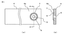
- FIG. 1A and 1B are diagrams showing a connection portion of a conductor connection structure according to Embodiment 1, wherein FIG. 1A is a plan view and FIG. 1B is a cross-sectional view taken along line AA in FIG.
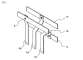
- FIG. 2 is a perspective view showing an example of use of the conductor connection structure of FIG.
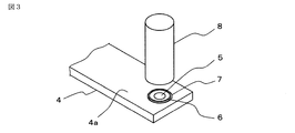
- FIG. 3 is an explanatory view of a method for processing the connecting portion of FIG. 1
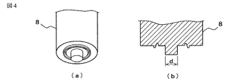
- FIG. 4 is a perspective view of a main part of a mold used for processing.
- the conductor to be connected is a flat plate having a rectangular cross section made of copper, aluminum, or an alloy thereof.
- the conductor is used in a power device such as a switch gear, and the connection portion of the main bus and the branch bus. Applies to However, the present invention is not limited to this, and can be applied to a conductor connection portion of an electric device in general.
- FIG. 2 is an example of a main bus and a branch bus arranged inside the switchgear, for example.
- Branch buses 2a, 2b, and 2c are combined with three-phase main buses 1a, 1b, and 1c arranged in the horizontal direction so that their connection surfaces are aligned, and are fastened and fixed by fastening members 3 including bolts and nuts.
- fastening members 3 including bolts and nuts.
- FIG. 1 is a diagram showing the shape of a through hole for fastening provided in a conductor connecting portion and its peripheral portion.
- the two conductors to be connected are, for example, a main bus and a branch bus, but in the following description, the conductor to be connected will be described as simply the conductor 4.
- a through hole 5 and an annular protrusion 6 concentrically with the through hole 5 are formed on the connection surface 4 a of one of the two conductors 4 to be connected. It is the characteristic part of this application.
- a concentric groove 7 is provided on the outer peripheral side of the protrusion 6, which is formed in the process of forming the protrusion 6 by a method described later.
- the cross-sectional shape of the protrusion 6 is preferably tapered toward the mating connection surface.
- the protrusion 6 is formed by a method such as pressing with a mold 8, for example.
- a through hole 5 is provided in advance in the conductor 4, the mold 8 is pressed so as to be concentric with the through hole 5, and the protrusion 6 is formed by pressing.
- the pressing surface of the mold 8 is as shown in FIG. 4 (a), and the cross-sectional shape of the pressing surface is as shown in FIG. 4 (b).
- the outer diameter d of the central cylindrical portion is a diameter that enters the through hole 5 of the conductor 4.
- the protrusion 6 is preferably subjected to silver plating, tin plating, or nickel plating in order to prevent corrosion and stabilize contact resistance.
- Plating may be applied to the entire conductor 4 or the entire connection surface 4a, but it is sufficient that the plating is applied to at least the protrusion 6 that contacts the connection surface of the mating conductor. By doing so, the plating range can be reduced and the cost can be reduced.
- the other conductor that is the counterpart conductor may be a non-plated conductor, that is, no plating. If there is no plating, an oxide film is formed. However, when the two conductors are bolted, the tip of the protrusion 6 bites into the connection surface of the other conductor and the oxide film is removed, so there is no need to perform plating. .
- connection surface of the other conductor of the connection partner is aligned with one conductor 4 formed as shown in FIG. 1, the bolt of the fastening member 3 is inserted into the through hole 5, and a nut is used.
- the tip of the concentrically formed protrusion 6 is in a state of being in line contact with the connecting surface of the mating conductor, reducing the contact resistance, and Can be stabilized.
- the line contact refers to a state in which at least the top portion of the protrusion 6 is in long contact with the contact surface of the other conductor in a line shape. Therefore, for example, it is possible to reduce the number of bolts to be tightened as compared with the conventional surface contact. Further, if the number of bolts is reduced, the connection work time is shortened.
- the conductor thickness is usually about several mm or more.
- the height of the protrusion 6 is too low, even if the protrusion 6 is provided, when it is tightened with a bolt, it becomes the same as the conventional surface contact without the protrusion 6, and it is possible to contact other than the protrusion 6. Sex comes out.
- the protrusion 6 is to be formed larger, it is necessary to increase the pressing force during processing, and the contact surface is distorted. In addition, the effect of “hanging” of the protrusion when tightened appears.
- the protrusion 6 can surely make a line contact and can be easily processed. I found out.
- the protrusions 6 are concentric circles, that is, concentric circles, but need not be concentric as long as the bolt tightening force is transmitted, and may be polygonal, for example.
- connection surface of the other conductor is aligned with the connection surface of one conductor, and the fastening member is used by using the through holes provided in each connection surface.
- a conductor connection structure to be fastened wherein an annular or polygonal groove is formed concentrically with the through-hole by pressing on the connection surface of one conductor, and a protrusion is formed by the rise of the groove. Is configured to be in line contact with the connection surface of the other conductor, the contact resistance of the conductor connection portion can be reduced in a stable state by line contact. For this reason, the number of bolts to be tightened can be reduced, and the working time for connection can be shortened.
- any one of silver plating, tin plating, and nickel plating is applied to the protrusion, corrosion can be prevented and the contact resistance of the connection surface can be stabilized.
- the other conductor to be connected to the one conductor on which the protruding portion is formed is a non-plated conductor, it is not necessary to perform plating, so that the cost can be reduced.
- the line can be reliably contacted with the protrusion when the conductor is connected, and the protrusion can be easily processed. It can be carried out.
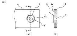
- FIG. 5A and 5B are diagrams showing a connection portion of the conductor connection structure according to the second embodiment, where FIG. 5A is a plan view and FIG. 5B is a cross-sectional view taken along line BB in FIG. It is a figure corresponding to FIG. 1 of Embodiment 1, the same part as FIG. 1 attaches
- the projecting portion is not formed by pressing, but the annular conductor 9 made of another member is used, and the annular conductor 9 is concentric with the through hole 5 on the connection surface 4a of one conductor 4. Arranged and joined by soldering, brazing, or pressure welding.
- the annular conductor 9 can be easily manufactured by punching from a thin plate of copper, aluminum or the like.
- the joined annular conductor 9 is the protrusion of the present embodiment.
- the annular conductor 9 may have a height of 0.1 mm or more and 3 mm or less and a width of 1 mm or more and 3 mm or less.
- the planar shape of the annular conductor 9 is a circular annular conductor in the figure, but is not limited to this and may be a polygonal shape.
- connection surface of one conductor is aligned with the connection surface of one conductor, and the fastening member is used by using the through holes provided in each connection surface.
- a conductor connecting structure to be fastened wherein a ring-shaped or polygonal conductor arranged concentrically with a through-hole is joined to the connecting surface of one conductor by soldering, brazing, or pressure welding Since the protrusion is configured to be in line contact with the connection surface of the other conductor, the protrusion can be formed without any special processing on the connection surface of the conductor, as in the first embodiment. In addition, the contact resistance of the conductor connecting portion can be reduced by line contact. Moreover, it is possible to easily apply plating only to the protrusions.
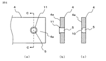
- FIG. 6A and 6B are diagrams showing a connection portion of the conductor connection structure according to the third embodiment, where FIG. 6A is a plan view, FIG. 6B is a cross-sectional view taken along the line CC in FIG. It is sectional drawing of CC in the middle. It is a figure corresponding to FIG. 1 of Embodiment 1, the same part as FIG. 1 attaches
- a small diameter portion 10 having a diameter smaller than the inner diameter of the through hole 5 is provided on the inner edge portion of the through hole 5 on the connection surface 4a side.
- a die not shown
- the protrusion 11 is formed.
- the mold to be pressed it is possible to form the projection 11 at the same time as the formation of the through hole 5, and the projection 11 can be easily formed.
- the size of the protrusion 11 is preferably the same as that of the first embodiment.
- connection surface of the other conductor is aligned with the connection surface of one conductor, and the fastening member is formed using the through holes provided in each connection surface.
- a conductor connection structure to be fastened wherein a small-diameter portion smaller than the inner diameter of the through-hole provided on the inner edge of the through-hole of one conductor is pressed from the opposite side of the connection surface to Since the protrusion is formed in a ring shape on the connection surface of the conductor, a protrusion having a diameter larger than the inner diameter of the through hole is formed, and the protrusion is configured to be in line contact with the connection surface of the other conductor.
- the contact resistance of the conductor connecting portion can be reduced by line contact.
- the contact resistance of the connection portion of the connection conductor used for the main bus, the branch bus, or the like is reduced. Can do.
- the embodiments can be freely combined, or the embodiments can be appropriately changed or omitted.
Landscapes
- Connections By Means Of Piercing Elements, Nuts, Or Screws (AREA)
- Gas-Insulated Switchgears (AREA)
Abstract
電気機器の母線接続等に適用され、一方の導体(4)の接続面(4a)に他方の導体の接続面を合わせ、それぞれの接続面に設けられた貫通穴(5)を利用し締結部材で締結する導体接続構造であって、一方の導体(4)の接続面(4a)に、押し加工によって貫通穴(5)と同心状に環状又は多角形状の溝(7)を形成し、溝(7)の分の盛り上がりにより突起部(6)が形成され、両方の導体が締付されたとき突起部(6)が他方の導体の接続面に線接触するように構成されている。
Description
この発明は、例えば、スイッチギヤ等の内部に収容される主母線や分岐母線等を接続する導体接続構造およびこの導体接続構造を用いたスイッチギヤに関するものである。
一般に、板状導体どうしを接続する場合の接触面は、面接触が広く用いられている。導体に流れる電流が増加すると、接続するボルトの本数を増やし、面接触の面積を増加させる手段がとられている。ボルト本数が増えると、特に導体接続箇所の多い電気設備では、組立作業や保守点検作業に多くの時間が必要となる。そこで、ボルト本数の削減や組立時間,保守点検時間の低減を目的として種々の導体接続構造が提案されている。
従来の導体接続構造として、例えば、貫通穴を有する2枚の導体の接続面間に、貫通穴と同心状に環状の挿入導体を挟み、貫通穴にボルトを挿入し、挿入導体を介して線接触で締め付ける構造が開示されている。環状の挿入導体の場合、組立時に貫通穴との位置調整が面倒なので、改善策として、一対の線状導体と位置決め部を持つ平板とを組み合わせた挿入導体も示されている(例えば、特許文献1参照)。
また、導体接続面に溝加工を施し、溝加工時に形成されたエッジを利用して導体接続面の接触抵抗を低減する接続構造が開示されている(例えば、特許文献2参照)。
従来の導体接続構造として、例えば、貫通穴を有する2枚の導体の接続面間に、貫通穴と同心状に環状の挿入導体を挟み、貫通穴にボルトを挿入し、挿入導体を介して線接触で締め付ける構造が開示されている。環状の挿入導体の場合、組立時に貫通穴との位置調整が面倒なので、改善策として、一対の線状導体と位置決め部を持つ平板とを組み合わせた挿入導体も示されている(例えば、特許文献1参照)。
また、導体接続面に溝加工を施し、溝加工時に形成されたエッジを利用して導体接続面の接触抵抗を低減する接続構造が開示されている(例えば、特許文献2参照)。
特許文献1に示すような、環状の挿入導体を介して導体の両面を接続する構造では、接触界面が2重となり抵抗が増える上、組立時に挿入導体の位置がずれやすく、ずれた場合はボルトの締付が挿入導体の一部に偏った状態で電圧が印加されてしまい、接続部の接触抵抗が増加するという問題があった。
また、特許文献1に示されている、線状導体と平板を組み合わせた挿入導体を介装する構造では、その挿入導体を製作するのにコストが掛かり、ボルトサイズやボルト本数が削減できても、コストメリットが得られないという問題があった。
また、特許文献2の接続構造の場合も、導体接続部の溝加工にコストが掛かるという問題があった。
また、特許文献1に示されている、線状導体と平板を組み合わせた挿入導体を介装する構造では、その挿入導体を製作するのにコストが掛かり、ボルトサイズやボルト本数が削減できても、コストメリットが得られないという問題があった。
また、特許文献2の接続構造の場合も、導体接続部の溝加工にコストが掛かるという問題があった。
この発明は、上記のような問題点を解決するためになされたもので、平板状の導体を重ね合わせてボルト接続する場合に、導体間の接触抵抗を低減し、ボルト本数の削減が可能な導体接続構造を得ることを目的とする。
この発明に係る導体接続構造は、一方の導体の接続面に他方の導体の接続面を合わせ、それぞれの接続面に設けられた貫通穴を利用して締結部材で締結する導体接続構造であって、一方の導体の接続面に、押し加工によって貫通穴と同心状に環状又は多角形状の溝を形成し、溝の分の盛り上がりにより突起部が形成され、突起部が他方の導体の接続面に線接触するように構成されているものである。
また、一方の導体の接続面に、貫通穴と同心状に配置された環状又は多角形状の導体が、はんだ付け,ろう付け,圧接のいずれかによって接合されて突起部が形成され、突起部が他方の導体の接続面に線接触するように構成されているものである。
また、一方の導体の貫通穴の接続面側の内縁部に設けられた、貫通穴の内径より小径の小径部が、接続面側の反対側から押圧されて一方の導体の接続面に環状に立ち上げられることにより貫通穴の内径より大径の突起部が形成され、突起部が他方の導体の接続面に線接触するように構成されているものである。
更に、この発明に係るスイッチギヤは、上記のいずれかに記載の導体接続構造を用いたものである。
また、一方の導体の接続面に、貫通穴と同心状に配置された環状又は多角形状の導体が、はんだ付け,ろう付け,圧接のいずれかによって接合されて突起部が形成され、突起部が他方の導体の接続面に線接触するように構成されているものである。
また、一方の導体の貫通穴の接続面側の内縁部に設けられた、貫通穴の内径より小径の小径部が、接続面側の反対側から押圧されて一方の導体の接続面に環状に立ち上げられることにより貫通穴の内径より大径の突起部が形成され、突起部が他方の導体の接続面に線接触するように構成されているものである。
更に、この発明に係るスイッチギヤは、上記のいずれかに記載の導体接続構造を用いたものである。
この発明の導体接続構造によれば、一方の導体の接続面に、押し加工によって貫通穴と同心状に環状又は多角形状の溝を形成し、溝の分の盛り上がりにより突起部が形成され、突起部が他方の導体の接続面に線接触するように構成されているので、線接触により導体接続部の接触抵抗を安定した状態で低減させることができる。このため、締め付けるボルト本数を削減することが可能となり、また、接続のための作業時間の短縮を図ることができる。
また、環状又は多角形状の導体が、はんだ付け,ろう付け,圧接のいずれかによって接合されて突起部が形成されているので、導体の接続面自体を加工することなく、上記と同様の効果を得ることができる。
また、一方の導体の貫通穴の接続面側の内縁部に設けられた、貫通穴の内径より小径の小径部が、接続面側の反対側から押圧されて一方の導体の接続面に環状に立ち上げられることにより貫通穴の内径より大径の突起部が形成されているので、容易に突起部が形成できて、上記と同様の効果を得ることができる。
更に、この発明のスイッチギヤによれば、主母線や分岐母線等に用いられる接続導体の接続部の接触抵抗を低減させることができる。
また、環状又は多角形状の導体が、はんだ付け,ろう付け,圧接のいずれかによって接合されて突起部が形成されているので、導体の接続面自体を加工することなく、上記と同様の効果を得ることができる。
また、一方の導体の貫通穴の接続面側の内縁部に設けられた、貫通穴の内径より小径の小径部が、接続面側の反対側から押圧されて一方の導体の接続面に環状に立ち上げられることにより貫通穴の内径より大径の突起部が形成されているので、容易に突起部が形成できて、上記と同様の効果を得ることができる。
更に、この発明のスイッチギヤによれば、主母線や分岐母線等に用いられる接続導体の接続部の接触抵抗を低減させることができる。
実施の形態1.
図1は、実施の形態1による導体接続構造の接続部を示す図であり、(a)は平面図、(b)は(a)の矢視A-Aの断面図である。図2は、図1の導体接続構造の使用例を示す斜視図である。また、図3は、図1の接続部の加工方法の説明図、図4は加工に用いる金型の要部斜視図である。
接続される導体は、銅、アルミ、又はそれらの合金から成る断面矩形状の平板であって、例えば、スイッチギヤのような電力機器の内部に使用されて、主母線と分岐母線の接続部等に適用されるものである。ただしこれに限定するものではなく、電気機器一般の導体接続部に適用可能である。
図1は、実施の形態1による導体接続構造の接続部を示す図であり、(a)は平面図、(b)は(a)の矢視A-Aの断面図である。図2は、図1の導体接続構造の使用例を示す斜視図である。また、図3は、図1の接続部の加工方法の説明図、図4は加工に用いる金型の要部斜視図である。
接続される導体は、銅、アルミ、又はそれらの合金から成る断面矩形状の平板であって、例えば、スイッチギヤのような電力機器の内部に使用されて、主母線と分岐母線の接続部等に適用されるものである。ただしこれに限定するものではなく、電気機器一般の導体接続部に適用可能である。
先ず、図2により本願の導体接続部の使用例から説明する。図2は、例えばスイッチギヤの内部に配置された主母線と分岐母線の一例である。
水平方向に向けて配置された3相の主母線1a,1b,1cに、分岐母線2a,2b,2cが、接続面を合わせて組み合わされ、ボルト,ナットからなる締結部材3で締め付けられて固定されている。このような導体どうしの接続部に本願の導体接続構造を適用するものである。
水平方向に向けて配置された3相の主母線1a,1b,1cに、分岐母線2a,2b,2cが、接続面を合わせて組み合わされ、ボルト,ナットからなる締結部材3で締め付けられて固定されている。このような導体どうしの接続部に本願の導体接続構造を適用するものである。
図1は、導体の接続部に設けた締結用の貫通穴とその周辺部の形状を示す図である。上記のように、接続する2枚の導体は、例えば主母線と分岐母線等であるが、以下の説明では接続される導体を単に導体4として説明する。
図1のように、接続する2枚の導体4のうちの一方の導体4の接続面4aに、貫通穴5と、その貫通穴5に対して同心状に環状の突起部6が形成されているのが本願の特徴部である。
突起部6の外周側には、同心状の溝7を有しているが、これは後述する方法で突起部6を形成する過程で形成されるものである。突起部6の断面形状は、相手の接続面側に向けて先細りにするのがよい。
図1のように、接続する2枚の導体4のうちの一方の導体4の接続面4aに、貫通穴5と、その貫通穴5に対して同心状に環状の突起部6が形成されているのが本願の特徴部である。
突起部6の外周側には、同心状の溝7を有しているが、これは後述する方法で突起部6を形成する過程で形成されるものである。突起部6の断面形状は、相手の接続面側に向けて先細りにするのがよい。
図3および図4により、突起部6の形成方法について説明する。
突起部6は、例えば金型8による押し加工等の方法で形成する。予め導体4に貫通穴5を設けておき、この貫通穴5に対して同心となるように金型8を押し付け、押し加工によって突起部6を形成する。金型8の押圧面は、図4(a)に示すとおりであり、押圧面の断面形状は、図4(b)のようになっている。中心の円筒部の外径dは、導体4の貫通穴5に入る径となっている。金型8を押圧して接続面4aに溝7を形成することで、その分が内周側に盛り上がり、環状の突起部6を容易に形成することができる。
なお、金型8の形状を工夫して、貫通穴5の加工と同時に、突起部6を形成するようにしても良い。
突起部6は、例えば金型8による押し加工等の方法で形成する。予め導体4に貫通穴5を設けておき、この貫通穴5に対して同心となるように金型8を押し付け、押し加工によって突起部6を形成する。金型8の押圧面は、図4(a)に示すとおりであり、押圧面の断面形状は、図4(b)のようになっている。中心の円筒部の外径dは、導体4の貫通穴5に入る径となっている。金型8を押圧して接続面4aに溝7を形成することで、その分が内周側に盛り上がり、環状の突起部6を容易に形成することができる。
なお、金型8の形状を工夫して、貫通穴5の加工と同時に、突起部6を形成するようにしても良い。
突起部6には、腐食を防止し接触抵抗を安定させるために銀めっき、錫めっき、ニッケルめっきのいずれかを施すのがよい。めっきは導体4全体、又は接続面4a全体に施しても良いが、少なくとも相手側の導体の接続面と接触する突起部6に施されていればよい。そうすることで、めっき範囲を少なくしコストを低減できる。
相手側導体である他方の導体は、無めっき導体、すなわち、めっき無しでも良い。めっきが無ければ酸化皮膜が形成されるが、両導体をボルト締めしたとき、突起部6の先端が他方の導体の接続面に食い込んで酸化皮膜が除去されるので、めっきを施さなくても良い。
相手側導体である他方の導体は、無めっき導体、すなわち、めっき無しでも良い。めっきが無ければ酸化皮膜が形成されるが、両導体をボルト締めしたとき、突起部6の先端が他方の導体の接続面に食い込んで酸化皮膜が除去されるので、めっきを施さなくても良い。
次に、作用について説明する。
突起部のない平面同士を接触させる場合は、面接触により接触面積が広いように見えるが、実際には不特定の複数箇所で点接触しており、接触部に偏りがあれば結果的に接触抵抗が増してしまう場合があった。また、接触抵抗を少なくするために、ボルト本数を増やす等の措置がとられていた。
これに対し、本実施の形態では、図1のように形成した一方の導体4に、接続相手の他方の導体の接続面を合わせ、貫通穴5に締結部材3のボルトを挿通し、ナットで締付固定されるが、締付力を加えることにより、同心状に形成された突起部6の先端が相手の導体の接続面に対し確実に線接触した状態となり、接触抵抗を低減させ、且つ、安定させることができる。
なお、ここで線接触とは、少なくとも突起部6の頂部が他方の導体の接触面に線状に長く接触する状態を言う。
このため、例えば、従来の面接触と比較して、締め付けるボルト本数を削減することが可能となる。また、ボルト本数が減れば、接続作業時間が短縮される。
突起部のない平面同士を接触させる場合は、面接触により接触面積が広いように見えるが、実際には不特定の複数箇所で点接触しており、接触部に偏りがあれば結果的に接触抵抗が増してしまう場合があった。また、接触抵抗を少なくするために、ボルト本数を増やす等の措置がとられていた。
これに対し、本実施の形態では、図1のように形成した一方の導体4に、接続相手の他方の導体の接続面を合わせ、貫通穴5に締結部材3のボルトを挿通し、ナットで締付固定されるが、締付力を加えることにより、同心状に形成された突起部6の先端が相手の導体の接続面に対し確実に線接触した状態となり、接触抵抗を低減させ、且つ、安定させることができる。
なお、ここで線接触とは、少なくとも突起部6の頂部が他方の導体の接触面に線状に長く接触する状態を言う。
このため、例えば、従来の面接触と比較して、締め付けるボルト本数を削減することが可能となる。また、ボルト本数が減れば、接続作業時間が短縮される。
次に、突起部6の大きさについて説明する。
本願の導体接続構造が適用される、例えばスイッチギヤの場合では、通常、導体厚さが数mm程度以上ある。もっと薄い導体の場合であれば、貫通穴を空けるときにバーリング加工等で、板厚全体を曲げて貫通穴の一面側に突出部を設けることも可能であるが、板厚が厚い場合は、上記のような金型8を用いて押し加工により突起部6を形成するのが効果的である。
ここで、突起部6の高さがあまり低いと、せっかく突起部6を設けてもボルトで締め付けたとき、突起部6のない従来の面接触と同様になり、突起部6以外でも接触する可能性が出てくる。逆に突起部6を大きく形成しようとすれば、加工時の押圧力を大きくする必要があり、接触面に歪みが生じてくる。又締め付けたときの突起部の「へたり」の影響が出てくる。
これらから、突起部6の高さを、0.1mm以上、3mm以下、また、突起部6の幅を1mm以上、3mm以下とすれば、突起部6で確実に線接触でき、加工も容易であることが分かった。
本願の導体接続構造が適用される、例えばスイッチギヤの場合では、通常、導体厚さが数mm程度以上ある。もっと薄い導体の場合であれば、貫通穴を空けるときにバーリング加工等で、板厚全体を曲げて貫通穴の一面側に突出部を設けることも可能であるが、板厚が厚い場合は、上記のような金型8を用いて押し加工により突起部6を形成するのが効果的である。
ここで、突起部6の高さがあまり低いと、せっかく突起部6を設けてもボルトで締め付けたとき、突起部6のない従来の面接触と同様になり、突起部6以外でも接触する可能性が出てくる。逆に突起部6を大きく形成しようとすれば、加工時の押圧力を大きくする必要があり、接触面に歪みが生じてくる。又締め付けたときの突起部の「へたり」の影響が出てくる。
これらから、突起部6の高さを、0.1mm以上、3mm以下、また、突起部6の幅を1mm以上、3mm以下とすれば、突起部6で確実に線接触でき、加工も容易であることが分かった。
図1では突起部6を同心の円形、つまり同心円状としているが、ボルトの締付力が伝達する範囲であれば、同心円状である必要はなく、例えば、多角形であっても良い。
以上のように、実施の形態1による導体接続構造によれば、一方の導体の接続面に他方の導体の接続面を合わせ、それぞれの接続面に設けられた貫通穴を利用して締結部材で締結する導体接続構造であって、一方の導体の接続面に、押し加工によって貫通穴と同心状に環状又は多角形状の溝を形成し、溝の分の盛り上がりにより突起部が形成され、突起部が他方の導体の接続面に線接触するように構成されているので、線接触により導体接続部の接触抵抗を安定した状態で低減させることができる。このため、締め付けるボルト本数を削減することが可能となり、接続のための作業時間の短縮を図ることができる。
また、突起部には、銀めっき、錫めっき、ニッケルめっきのいずれかが施されているので、腐食を防止して接続面の接触抵抗を安定化できる。
また、突起部が形成された一方の導体に対して接続相手となる他方の導体は、無めっき導体としたので、めっきをする必要がないためコストを低減できる。
また、突起部の高さが0.1mm以上,3mm以下であり、幅が1mm以上,3mm以下としたので、導体接続時に突起部で確実に線接触でき、また、突起部の加工を容易に行うことができる。
実施の形態2.
図5は、実施の形態2による導体接続構造の接続部を示す図であり、(a)は平面図、(b)は(a)の矢視B-Bの断面図である。実施の形態1の図1に対応する図であり、図1と同等部分は同一符号を付して説明は省略する。以下相違点を中心に説明する。
図5は、実施の形態2による導体接続構造の接続部を示す図であり、(a)は平面図、(b)は(a)の矢視B-Bの断面図である。実施の形態1の図1に対応する図であり、図1と同等部分は同一符号を付して説明は省略する。以下相違点を中心に説明する。
本実施の形態では、突起部を押し加工で形成するのではなく、別部材からなる環状導体9を用いて、一方の導体4の接続面4aに、環状導体9を貫通穴5に同心状に配置し、はんだ付け,ろう付け,圧接のいずれかにより接合するものである。環状導体9は、銅,アルミ等の薄板から打ち抜き加工で容易に製作することが可能である。接合された環状導体9が本実施の形態の突起部である。
環状導体9の大きさは、実施の形態1と同様に、高さを、0.1mm以上,3mm以下、幅を1mm以上,3mm以下とすればよい。
また、環状導体9の平面形状は、図では円形の環状導体としているが、これに限定せず多角形状であっても良い。
環状導体9の大きさは、実施の形態1と同様に、高さを、0.1mm以上,3mm以下、幅を1mm以上,3mm以下とすればよい。
また、環状導体9の平面形状は、図では円形の環状導体としているが、これに限定せず多角形状であっても良い。
以上のように、実施の形態2による導体接続構造によれば、一方の導体の接続面に他方の導体の接続面を合わせ、それぞれの接続面に設けられた貫通穴を利用して締結部材で締結する導体接続構造であって、一方の導体の接続面に、貫通穴と同心状に配置された環状又は多角形状の導体が、はんだ付け,ろう付け,圧接のいずれかによって接合されて突起部が形成され、突起部が他方の導体の接続面に線接触するように構成されているので、導体の接続面自体に特別な加工をすることなく突起部が形成でき、実施の形態1と同様に、線接触により導体接続部の接触抵抗を低減させることができる。また、突起部のみに容易にめっきを施すことが可能である。
実施の形態3.
図6は、実施の形態3による導体接続構造の接続部を示す図であり、(a)は平面図、(b)は(a)の矢視C-Cの断面図、(c)は加工途中の矢視C-Cの断面図である。実施の形態1の図1に対応する図であり、図1と同等部分は同一符号を付して説明は省略する。以下相違点を中心に説明する。
図6は、実施の形態3による導体接続構造の接続部を示す図であり、(a)は平面図、(b)は(a)の矢視C-Cの断面図、(c)は加工途中の矢視C-Cの断面図である。実施の形態1の図1に対応する図であり、図1と同等部分は同一符号を付して説明は省略する。以下相違点を中心に説明する。
図6(c)に示すように、貫通穴5を加工する際に、接続面4a側の貫通穴5の内縁部に、貫通穴5の内径より径が小さい小径部10を設けておく。
次に、貫通穴5の小径部10の反対側から金型(図示せず)で押圧して、小径部10を接続面4aの表面側に環状に立ち上げることによって、図6(b)のように突起部11を形成するものである。
押圧する金型を工夫することで、貫通穴5の形成と同時の突起部11を形成することも可能であり、突起部11の形成が容易にできる。
なお、突起部11の大きさは、実施の形態1と同様にするのが良い。
次に、貫通穴5の小径部10の反対側から金型(図示せず)で押圧して、小径部10を接続面4aの表面側に環状に立ち上げることによって、図6(b)のように突起部11を形成するものである。
押圧する金型を工夫することで、貫通穴5の形成と同時の突起部11を形成することも可能であり、突起部11の形成が容易にできる。
なお、突起部11の大きさは、実施の形態1と同様にするのが良い。
以上のように、実施の形態3の導体接続構造によれば、一方の導体の接続面に他方の導体の接続面を合わせ、それぞれの接続面に設けられた貫通穴を利用して締結部材で締結する導体接続構造であって、一方の導体の貫通穴の接続面側の内縁部に設けられた、貫通穴の内径より小径の小径部が、接続面側の反対側から押圧されて一方の導体の接続面に環状に立ち上げられることにより貫通穴の内径より大径の突起部が形成され、突起部が他方の導体の接続面に線接触するように構成されているので、突起部を容易に形成でき、実施の形態1と同様に、線接触により導体接続部の接触抵抗を低減させることができる。
また、実施の形態1から実施の形態3のいずれかに記載の導体接続構造を用いたスイッチギヤによれば、主母線や分岐母線等に用いられる接続導体の接続部の接触抵抗を低減させることができる。
なお、本願発明は、その発明の範囲内において、各実施の形態を自由に組み合わせたり、各実施の形態を適宜、変更、省略したりすることが可能である。
1a,1b,1c 主母線、2a,2b,2c 分岐母線、
3 締結部材、4 導体、4a 接続面、5 貫通穴、
6 突起部、7 溝、8 金型、9 環状導体、
10 小径部、11 突起部。
3 締結部材、4 導体、4a 接続面、5 貫通穴、
6 突起部、7 溝、8 金型、9 環状導体、
10 小径部、11 突起部。
Claims (7)
- 一方の導体の接続面に他方の導体の接続面を合わせ、それぞれの前記接続面に設けられた貫通穴を利用して締結部材で締結する導体接続構造であって、
前記一方の導体の接続面に、押し加工によって前記貫通穴と同心状に環状又は多角形状の溝を形成し、前記溝の分の盛り上がりにより突起部が形成され、前記突起部が前記他方の導体の接続面に線接触するように構成されていることを特徴とする導体接続構造。 - 一方の導体の接続面に他方の導体の接続面を合わせ、それぞれの前記接続面に設けられた貫通穴を利用して締結部材で締結する導体接続構造であって、
前記一方の導体の接続面に、前記貫通穴と同心状に配置された環状又は多角形状の導体が、はんだ付け,ろう付け,圧接のいずれかによって接合されて突起部が形成され、前記突起部が前記他方の導体の接続面に線接触するように構成されていることを特徴とする導体接続構造。 - 一方の導体の接続面に他方の導体の接続面を合わせ、それぞれの前記接続面に設けられた貫通穴を利用して締結部材で締結する導体接続構造であって、
前記一方の導体の前記貫通穴の接続面側の内縁部に設けられた、前記貫通穴の内径より小径の小径部が、前記接続面側の反対側から押圧されて前記一方の導体の接続面に環状に立ち上げられることにより前記貫通穴の内径より大径の突起部が形成され、前記突起部が前記他方の導体の接続面に線接触するように構成されていることを特徴とする導体接続構造。 - 請求項1から請求項3のいずれか1項に記載に導体接続構造において、
前記突起部には、銀めっき、錫めっき、ニッケルめっきのいずれかが施されていることを特徴とする導体接続構造。 - 請求項4記載の導体接続構造において、
前記他方の導体は、無めっき導体が用いられていることを特徴とする導体接続構造。 - 請求項1から請求項5のいずれか1項に記載に導体接続構造において、
前記突起部の高さが0.1mm以上,3mm以下であり、幅が1mm以上,3mm以下であることを特徴とする導体接続構造。 - 請求項1から請求項6のいずれか1項に記載の導体接続構造を用いたスイッチギヤ。
Priority Applications (1)
| Application Number | Priority Date | Filing Date | Title |
|---|---|---|---|
| JP2015541449A JP5989255B2 (ja) | 2013-10-09 | 2014-06-09 | 導体接続構造およびこれを用いたスイッチギヤ |
Applications Claiming Priority (2)
| Application Number | Priority Date | Filing Date | Title |
|---|---|---|---|
| JP2013-211793 | 2013-10-09 | ||
| JP2013211793 | 2013-10-09 |
Publications (1)
| Publication Number | Publication Date |
|---|---|
| WO2015052955A1 true WO2015052955A1 (ja) | 2015-04-16 |
Family
ID=52812777
Family Applications (1)
| Application Number | Title | Priority Date | Filing Date |
|---|---|---|---|
| PCT/JP2014/065195 Ceased WO2015052955A1 (ja) | 2013-10-09 | 2014-06-09 | 導体接続構造およびこれを用いたスイッチギヤ |
Country Status (2)
| Country | Link |
|---|---|
| JP (1) | JP5989255B2 (ja) |
| WO (1) | WO2015052955A1 (ja) |
Cited By (2)
| Publication number | Priority date | Publication date | Assignee | Title |
|---|---|---|---|---|
| WO2019101588A1 (de) * | 2017-11-24 | 2019-05-31 | Siemens Aktiengesellschaft | Elektrische kontaktierungsschnittstelle mit einem geringen und stabilen elektrischen übergangswiderstand |
| WO2024131958A1 (zh) * | 2022-12-24 | 2024-06-27 | 长春捷翼汽车科技股份有限公司 | 一种电连接结构 |
Citations (6)
| Publication number | Priority date | Publication date | Assignee | Title |
|---|---|---|---|---|
| JPS56110584U (ja) * | 1980-01-28 | 1981-08-26 | ||
| JPS5976072U (ja) * | 1982-11-15 | 1984-05-23 | 松下電工株式会社 | 端子装置 |
| JPH07192827A (ja) * | 1993-12-24 | 1995-07-28 | Sumitomo Wiring Syst Ltd | 電気自動車の高圧大電流分電装置用接続導体 |
| JP2005222811A (ja) * | 2004-02-05 | 2005-08-18 | Pioneer Electronic Corp | 導通装置 |
| JP2012009411A (ja) * | 2010-05-24 | 2012-01-12 | Japan Aviation Electronics Industry Ltd | 導体接続ワッシャ、それを使った接続機構及び導体接続ワッシャの製造方法 |
| JP2012038563A (ja) * | 2010-08-06 | 2012-02-23 | Auto Network Gijutsu Kenkyusho:Kk | 電気的接続構造 |
Family Cites Families (2)
| Publication number | Priority date | Publication date | Assignee | Title |
|---|---|---|---|---|
| JPH11185842A (ja) * | 1997-12-17 | 1999-07-09 | Yazaki Corp | 板状部材の積層固定構造 |
| JP5665643B2 (ja) * | 2011-04-26 | 2015-02-04 | 三菱電機株式会社 | スイッチギヤ |
-
2014
- 2014-06-09 WO PCT/JP2014/065195 patent/WO2015052955A1/ja not_active Ceased
- 2014-06-09 JP JP2015541449A patent/JP5989255B2/ja active Active
Patent Citations (6)
| Publication number | Priority date | Publication date | Assignee | Title |
|---|---|---|---|---|
| JPS56110584U (ja) * | 1980-01-28 | 1981-08-26 | ||
| JPS5976072U (ja) * | 1982-11-15 | 1984-05-23 | 松下電工株式会社 | 端子装置 |
| JPH07192827A (ja) * | 1993-12-24 | 1995-07-28 | Sumitomo Wiring Syst Ltd | 電気自動車の高圧大電流分電装置用接続導体 |
| JP2005222811A (ja) * | 2004-02-05 | 2005-08-18 | Pioneer Electronic Corp | 導通装置 |
| JP2012009411A (ja) * | 2010-05-24 | 2012-01-12 | Japan Aviation Electronics Industry Ltd | 導体接続ワッシャ、それを使った接続機構及び導体接続ワッシャの製造方法 |
| JP2012038563A (ja) * | 2010-08-06 | 2012-02-23 | Auto Network Gijutsu Kenkyusho:Kk | 電気的接続構造 |
Cited By (3)
| Publication number | Priority date | Publication date | Assignee | Title |
|---|---|---|---|---|
| WO2019101588A1 (de) * | 2017-11-24 | 2019-05-31 | Siemens Aktiengesellschaft | Elektrische kontaktierungsschnittstelle mit einem geringen und stabilen elektrischen übergangswiderstand |
| US11444391B2 (en) | 2017-11-24 | 2022-09-13 | Siemens Aktiengesellschaft | Electrical contacting interface with a low and stable electrical transfer resistance |
| WO2024131958A1 (zh) * | 2022-12-24 | 2024-06-27 | 长春捷翼汽车科技股份有限公司 | 一种电连接结构 |
Also Published As
| Publication number | Publication date |
|---|---|
| JPWO2015052955A1 (ja) | 2017-03-09 |
| JP5989255B2 (ja) | 2016-09-07 |
Similar Documents
| Publication | Publication Date | Title |
|---|---|---|
| US20200021045A1 (en) | Electric wire with terminal and method of manufacturing the same | |
| KR20110128729A (ko) | 도체 접속 와셔, 그것을 사용한 접속기구 및 도체 접속 와셔의 제조방법 | |
| JP6652583B2 (ja) | 端子付き電線 | |
| US11870193B2 (en) | Busbar unit and method of manufacturing busbar unit | |
| US8979602B2 (en) | Electrical male terminal | |
| JP2005353567A (ja) | プレスフィット端子およびそれを用いた回路基板モジュール | |
| US9666956B2 (en) | Minute current crimping terminal and minute current wire harness | |
| JP2017216078A (ja) | プレスフィット端子 | |
| CN102656748B (zh) | 大电流接触组件以及相应的用于制造大电流接触装置的方法 | |
| CN108123242A (zh) | 同轴电连接器及其制造方法 | |
| WO2015118974A1 (ja) | 配電部材 | |
| JP5989255B2 (ja) | 導体接続構造およびこれを用いたスイッチギヤ | |
| EP3553892A1 (en) | Terminalized electric wire | |
| US10069219B2 (en) | Plug-type connection having a conical clamping ring clamping a conical collet | |
| JP6387441B1 (ja) | 端子圧着装置及び端子圧着方法 | |
| WO2017104388A1 (ja) | 端子金具及びコネクタ | |
| JP5063672B2 (ja) | 配線基板及びその製造方法 | |
| JP2010009789A (ja) | 端子金具及び端子付き電線 | |
| JP2019186082A (ja) | 電磁圧接端子および電磁圧接端子の製造方法並びに接続端子 | |
| DE202011106222U1 (de) | Bimetallischer Terminaladapter | |
| JP2018198150A (ja) | 差し込み端子装置および開閉器 | |
| US20250323429A1 (en) | Connection arrangement, in particular for use in electric vehicles or hybrid vehicles | |
| JP2017084576A (ja) | 導電接続構造 | |
| JP2017216212A (ja) | バスバー連結構造 | |
| JP4921247B2 (ja) | コネクタ及びその製造方法、アーク放電低減方法 |
Legal Events
| Date | Code | Title | Description |
|---|---|---|---|
| 121 | Ep: the epo has been informed by wipo that ep was designated in this application |
Ref document number: 14851569 Country of ref document: EP Kind code of ref document: A1 |
|
| ENP | Entry into the national phase |
Ref document number: 2015541449 Country of ref document: JP Kind code of ref document: A |
|
| NENP | Non-entry into the national phase |
Ref country code: DE |
|
| 122 | Ep: pct application non-entry in european phase |
Ref document number: 14851569 Country of ref document: EP Kind code of ref document: A1 |