WO2015052995A1 - Dispositif laser à semi-conducteurs et procédé de fabrication pour ce dernier - Google Patents
Dispositif laser à semi-conducteurs et procédé de fabrication pour ce dernier Download PDFInfo
- Publication number
- WO2015052995A1 WO2015052995A1 PCT/JP2014/071828 JP2014071828W WO2015052995A1 WO 2015052995 A1 WO2015052995 A1 WO 2015052995A1 JP 2014071828 W JP2014071828 W JP 2014071828W WO 2015052995 A1 WO2015052995 A1 WO 2015052995A1
- Authority
- WO
- WIPO (PCT)
- Prior art keywords
- optical member
- semiconductor laser
- cap
- ceiling wall
- laser device
- Prior art date
- Legal status (The legal status is an assumption and is not a legal conclusion. Google has not performed a legal analysis and makes no representation as to the accuracy of the status listed.)
- Ceased
Links
Images






Classifications
-
- H—ELECTRICITY
- H01—ELECTRIC ELEMENTS
- H01S—DEVICES USING THE PROCESS OF LIGHT AMPLIFICATION BY STIMULATED EMISSION OF RADIATION [LASER] TO AMPLIFY OR GENERATE LIGHT; DEVICES USING STIMULATED EMISSION OF ELECTROMAGNETIC RADIATION IN WAVE RANGES OTHER THAN OPTICAL
- H01S5/00—Semiconductor lasers
- H01S5/02—Structural details or components not essential to laser action
- H01S5/022—Mountings; Housings
- H01S5/0225—Out-coupling of light
- H01S5/02253—Out-coupling of light using lenses
-
- H—ELECTRICITY
- H01—ELECTRIC ELEMENTS
- H01S—DEVICES USING THE PROCESS OF LIGHT AMPLIFICATION BY STIMULATED EMISSION OF RADIATION [LASER] TO AMPLIFY OR GENERATE LIGHT; DEVICES USING STIMULATED EMISSION OF ELECTROMAGNETIC RADIATION IN WAVE RANGES OTHER THAN OPTICAL
- H01S5/00—Semiconductor lasers
- H01S5/02—Structural details or components not essential to laser action
- H01S5/022—Mountings; Housings
- H01S5/023—Mount members, e.g. sub-mount members
- H01S5/0231—Stems
-
- H—ELECTRICITY
- H01—ELECTRIC ELEMENTS
- H01S—DEVICES USING THE PROCESS OF LIGHT AMPLIFICATION BY STIMULATED EMISSION OF RADIATION [LASER] TO AMPLIFY OR GENERATE LIGHT; DEVICES USING STIMULATED EMISSION OF ELECTROMAGNETIC RADIATION IN WAVE RANGES OTHER THAN OPTICAL
- H01S5/00—Semiconductor lasers
- H01S5/02—Structural details or components not essential to laser action
- H01S5/022—Mountings; Housings
- H01S5/02208—Mountings; Housings characterised by the shape of the housings
- H01S5/02212—Can-type, e.g. TO-CAN housings with emission along or parallel to symmetry axis
Definitions
- the present invention relates to a semiconductor laser device including an optical member such as a lens and a method for manufacturing the same.
- FIG. 15 is a front sectional view of a conventional semiconductor laser device.
- a semiconductor laser element 4 that emits laser light from an emission region 4 a is fixed to a stem 2 via a submount 3.
- a metal cap 5 that covers the semiconductor laser element 4 is provided on the stem 2.
- the cap 5 is formed in a bottomed cylindrical shape having a peripheral wall 5a and a ceiling wall 5b, and a flange portion 5d protruding in the outer peripheral direction from the lower end of the peripheral wall 5a is fixed to the stem 2.
- a window portion 5c facing the emission region 4a of the semiconductor laser element 4 is opened in the ceiling wall 5b.
- a transparent optical member 6 that closes the window 5c is disposed on the ceiling wall 5b of the cap 5. Thereby, the inside of the cap 5 is sealed.
- the optical member 6 has a curved light exit surface 6a and forms a lens.
- Laser light emitted from the emission region 4a of the semiconductor laser element 4 enters the optical member 6 through the window portion 5c, and is condensed and emitted from the light emission surface 6a of the optical member 6.
- the optical member 6 is generally formed of glass having a small lens aberration for applications such as optical communication.
- the use of infrared lasers is expanding as the output of semiconductor laser devices that emit infrared rays increases, the performance of light receiving sensors increases, or the speed of arithmetic circuits increases.
- the demand as a light source for sensors for the purpose of three-dimensional measurement is rapidly spreading.
- the laser light may be scattered and irradiated over a wide range, and lens aberrations are not a big problem.
- the optical member 6 of the semiconductor laser device 1 is formed of an epoxy or silicone resin, the material cost is low and the processing is easy, so that the cost of the semiconductor laser device 1 can be reduced. Therefore, there is a possibility that the semiconductor laser device 1 using the resin optical member 6 will be widely used in the future.
- the optical member 6 is provided to scatter laser light from the viewpoint of eye-safety to increase the apparent light source (virtual light source) and suppress energy concentration on the retina.
- the optical member 6 may fall off due to an external force F or the like as shown in FIG.
- the laser light emitted from the emission region 4a is directly emitted into the space through the window 5c as indicated by the arrow E, and thus there is a problem that the safety of the semiconductor laser device 1 is low.
- the optical member 6 when the optical member 6 is formed of an epoxy resin, it has a high adhesive force with respect to the metal cap 5. However, when the semiconductor laser device 1 is exposed to a high temperature by reflow or the like after the high temperature and high humidity test, the optical member 6 may be peeled off at the interface with the cap 5. For this reason, similarly to the above, there is a problem that the safety of the semiconductor laser device 1 is low.
- Patent Documents 1 and 2 disclose a semiconductor laser device 1 that can prevent the optical member 6 from falling off the cap 5.
- the base material of the optical member 6 made of glass and the cap 5 are disposed in the space between the upper mold and the lower mold of the mold, and the base material is heated and melted.
- the optical member 6 having convex surfaces on both sides can sandwich the ceiling wall 5b via the window portion 5c, and the optical member 6 can be prevented from falling off.
- the resin-made optical member 6 can also be formed by a similar mold.
- the optical member 6 having a convex shape on both sides and the cap 5 are integrally formed by injection molding in which a resin is injected into the space between the upper mold and the lower mold of the mold. The Thereby, dropping of the optical member 6 can be prevented.
- Japanese Unexamined Patent Publication No. 2006-301352 pages 4 to 7, FIGS. 2 and 3) Japanese Patent Laid-Open No. 9-205251 (pages 3-5, FIG. 3) Japanese Patent Application Laid-Open No. 59-218430 (first page-second page, FIGS. 1 and 4)
- An object of the present invention is to provide a semiconductor laser device that can improve safety and reduce costs, and a manufacturing method thereof.
- the present invention provides a semiconductor laser element that emits laser light from an emission region, a peripheral wall and a ceiling wall that cover the semiconductor laser element, and a window portion that faces the emission region on the ceiling wall.
- a semiconductor laser device including an open cap and a transparent optical member that closes the window, the optical member is formed by curing a liquid resin, and the ceiling wall is sandwiched between the optical member and the optical member.
- a light incident surface facing the emission region of the member is formed by natural flow of the liquid resin.
- the present invention is characterized in that, in the semiconductor laser device having the above configuration, the optical member is made of a thermosetting resin or an ultraviolet curable resin.
- the present invention is also characterized in that, in the semiconductor laser device having the above configuration, the optical member contains a scattering material.
- the optical member has an extending portion that extends continuously on the outer peripheral surface of the peripheral wall from the ceiling wall and is in contact with the inner peripheral surface of the peripheral wall.
- the peripheral wall is sandwiched between the optical members.
- the present invention also includes a semiconductor laser element that emits laser light from an emission region, a cap that has a peripheral wall and a ceiling wall that covers the semiconductor laser element, and a window that faces the emission region and that opens to the ceiling wall;
- a semiconductor laser device comprising a transparent optical member that closes a window, A molding die provided with a concave portion that forms a light emitting surface of the optical member, and a large-diameter portion that is formed with an enlarged diameter at an opening end of the concave portion and into which the cap is fitted, and the liquid resin is formed into the concave portion
- the cap is inserted into the enlarged diameter portion with the ceiling wall facing downward, and the natural fluid flows through the window portion into the inner surface of the ceiling wall.
- the liquid member is cured to form the optical member that sandwiches the ceiling wall.
- the cap in the method of manufacturing a semiconductor laser device having the above-described structure, has a flange portion that protrudes in an outer peripheral direction at an end portion on the opposite side to the ceiling wall, and is hooked on the flange portion so that the cap Is provided with a latching member that is inserted into and removed from the enlarged diameter portion.
- the transparent optical member that closes the opening of the cap sandwiches the ceiling wall of the cap, and the light incident surface of the optical member is formed by the natural flow of the liquid resin.
- the optical member can be prevented from falling off, and the optical member can be formed by a simple device. Therefore, it is possible to improve the safety and reduce the cost of the semiconductor laser device.
- the cap after injecting the liquid resin injected into the concave portion of the mold and on the bottom surface of the enlarged diameter portion, the cap is inserted into the enlarged diameter portion, and the natural fluid flows through the window portion into the inner surface of the ceiling wall.
- the liquid resin is cured.
- the optical member which can prevent the drop-off from the cap can be easily formed. Further, it is possible to prevent the generation of an air layer or bubbles when forming the optical member. Therefore, it is possible to improve the safety and reduce the cost of the semiconductor laser device.
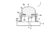
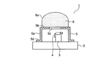
- 1 is a front sectional view showing a semiconductor laser device according to a first embodiment of the present invention.
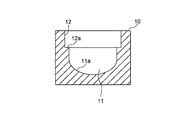
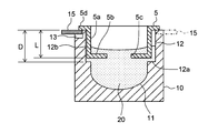
- 1 is a front sectional view showing a molding die for an optical member of a semiconductor laser device according to a first embodiment of the present invention.
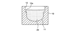
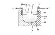
- Front sectional drawing which shows the state which inject
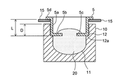
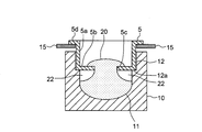
- Front sectional drawing which shows the state which installed the cap in the shaping
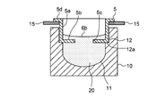
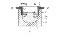
- Front sectional drawing which shows the state at the time of hardening of the optical member of the semiconductor laser apparatus of 1st Embodiment of this invention
- Front sectional drawing which shows the state which inject
- Front sectional drawing which shows the state in which liquid resin is inject
- Front sectional drawing which shows the state by which liquid resin is inject
- Front sectional drawing which shows the state in which the bubble of the optical member of the semiconductor laser apparatus of 1st Embodiment of this invention was formed
- Front sectional drawing which shows the state which applied external force to the optical member of the semiconductor laser apparatus of 1st Embodiment of this invention
- FIG. 1 is a front sectional view of the semiconductor laser device of the first embodiment.
- the same reference numerals are assigned to the same parts as those in the conventional example shown in FIG.
- the semiconductor laser device 1 has a semiconductor laser element 4 that emits laser light such as infrared rays from an emission region 4 a, and the semiconductor laser element 4 is fixed to the stem 2 via a submount 3.
- a metal cap 5 that covers the semiconductor laser element 4 is provided on the stem 2.
- the cap 5 is formed in a bottomed cylindrical shape having a peripheral wall 5a and a ceiling wall 5b. At the lower end of the peripheral wall 5a, which is the opposite end of the ceiling wall 5b, a flange 5d projects outward, and the flange 5d is fixed to the stem 2.
- a window portion 5c facing the emission region 4a of the semiconductor laser element 4 is opened in the ceiling wall 5b.
- a transparent optical member 6 that closes the window 5c is disposed on the ceiling wall 5b of the cap 5. Thereby, the inside of the cap 5 is sealed.
- the optical member 6 sandwiches the ceiling wall 5b through the window 5c, and forms a lens having a convex light exit surface 6a and a substantially flat light entrance surface 6b facing the exit region 4a.
- the optical member 6 is formed of a thermosetting resin, and the light incident surface 6b is formed by natural flow of the thermosetting resin as will be described in detail later.
- the laser light emitted from the emission region 4a of the semiconductor laser element 4 enters the optical member 6 through the light emission surface 6a.
- the laser light incident on the optical member 6 is condensed and emitted from the light emission surface 6 a of the optical member 6.
- the optical member 6 Since the optical member 6 is made of resin, the aberration is large and the amount of scattered scattered light is larger than when the optical member 6 is made of glass. For this reason, the semiconductor laser device 1 is used for applications such as a sensor light source that irradiates laser light over a wide range. At this time, the apparent light source becomes large due to the scattering of the laser light, and the energy concentration on the retina can be suppressed.
- the optical member 6 may contain a scattering material such as silica. Thereby, the amount of scattering of the emitted light can be further increased, and energy concentration on the retina can be further suppressed.
- FIG. 2 shows a front sectional view of a mold for forming the optical member 6.
- the mold 10 is made of resin or the like, and has a recess 11 having an open upper surface and a diameter-enlarged portion 12 formed by expanding the diameter of the opening end of the recess 11.
- the light emitting surface 6a (see FIG. 1) of the optical member 6 is formed by the shape of the inner surface 11a of the recess 11.
- the enlarged diameter portion 12 is formed to have an inner diameter with which the peripheral wall 5a (see FIG. 1) of the cap 5 is fitted, and the cap 5 is inserted.
- FIGS. 3 to 5 are front sectional views sequentially showing steps of forming the optical member 6 by the molding die 10. As shown in FIG. 3, a liquid resin 20 of a thermosetting resin is injected into the concave portion 11 of the mold 10 and the bottom surface 12 a of the enlarged diameter portion 12.
- the flange 5 d of the cap 5 is hooked by the hooking member 15, the hooking member 15 is lowered, the ceiling wall 5 b is directed downward, and the cap 5 becomes the enlarged diameter portion 12. Inserted. As a result, the ceiling wall 5b of the cap 5 is placed on the bottom surface 12a of the enlarged diameter portion 12 and immersed in the liquid resin 20, and the liquid resin 20 enters the inner surface of the ceiling wall 5b through the window portion 5c.
- the distance L between the upper surface (downward in the figure) of the ceiling wall 5b of the cap 5 and the upper surface (downward in the figure) of the flange 5d is greater than the depth D of the enlarged diameter portion 12.
- the retaining member 15 is disposed in the gap between the upper surface of the mold 10 and the flange portion 5 d, and the cap 5 can be easily inserted into the enlarged diameter portion 12.
- the liquid resin 20 naturally flows on the inner surface of the ceiling wall 5b and reaches the inner peripheral surface of the peripheral wall 5a. Thereafter, the liquid resin 20 is cured by raising the temperature of the mold 10, and a resin optical member 6 (see FIG. 1) sandwiching the ceiling wall 5 b is formed. And the optical member 6 is taken out from the shaping
- the light incident surface 6b of the optical member 6 is formed by the natural flow of the liquid resin 20, and is slightly concave and substantially flat due to the surface tension of the liquid resin 20 and the shrinkage during curing. By varying the curing conditions, viscosity, or volatile components of the curing agent of the liquid resin 20, the light incident surface 6b can be formed with a desired curvature.
- the optical member 6 can be easily formed by a simple device having the single mold 10, and the cost of the semiconductor laser device 1 can be reduced.
- the liquid resin 20 when the liquid resin 20 is injected after the cap 5 is inserted into the enlarged diameter portion 12, there are the following problems. That is, as shown in FIG. 7, the liquid resin 20 may block the window portion 5 c due to surface tension, and an air layer 21 may be formed between the ceiling wall 5 b and the liquid resin 20 in the recess 11. For this reason, the optical member 6 is not fixed on the ceiling wall 5b by the air layer 21, and the yield of the optical member 6 is reduced. Although the air layer 21 can be suppressed by making the diameter of the nozzle for injecting the liquid resin 20 smaller than the window portion 5c, the number of steps increases because the nozzle is easily clogged.
- the cap 5 is inserted into the enlarged diameter portion 12 to improve the yield of the optical member 6. it can.
- the optical member 6 is firmly fixed because it sandwiches the ceiling wall 5b of the cap 5, and the optical member 6 can be prevented from dropping due to a decrease in adhesive force or external force. At this time, since the optical member 6 contacts the inner peripheral surface of the peripheral wall 5a of the cap 5, the optical member 6 can be more firmly fixed.
- the transparent optical member 6 that closes the window 5c of the cap 5 sandwiches the ceiling wall 5b of the cap 5, and the light incident surface 6b of the optical member 6 is formed by the natural flow of the liquid resin 20.
- the optical member 6 can be prevented from falling off, and the optical member 6 can be formed by a simple device. Therefore, the safety and cost reduction of the semiconductor laser device 1 can be achieved.
- the optical member 6 is made of a thermosetting resin, the optical member 6 can be easily formed by injecting the liquid resin 20 into one mold 10 and thermosetting.
- the optical member 6 contains a scattering material such as silica, the safety of the retina when using the semiconductor laser device 1 can be improved.
- the cap 5 is inserted in the enlarged diameter part 12, and it penetrate
- the cap 5 can be easily inserted into and removed from the enlarged diameter portion 12 of the mold 10.
- FIG. 11 shows a front sectional view of the semiconductor laser device 1 of the second embodiment.
- the same reference numerals are given to the same parts as those of the first embodiment shown in FIGS.
- the shape of the optical member 6 is different from that of the first embodiment.
- Other parts are the same as those of the first embodiment.
- the optical member 6 has a light exit surface 6 a formed by a flat surface, and seals the inside of the cap 5. As a result, the semiconductor laser device 1 is emitted from the emission region 4 a of the semiconductor laser element 4 without being condensed.
- the same effect as that of the first embodiment can be obtained.
- the same effect can be obtained even if the light emitting surface 6a of the optical member 6 is formed as a concave surface.
- FIG. 12 shows a front sectional view of the semiconductor laser device 1 of the third embodiment.
- the same reference numerals are given to the same parts as those of the first embodiment shown in FIGS.
- the shape of the optical member 6 is different from that of the first embodiment.
- Other parts are the same as those of the first embodiment.
- the optical member 6 has an extending portion 6 c that extends from the ceiling wall 5 b of the cap 5 continuously on the outer peripheral surface of the peripheral wall 5 a.
- the optical member 6 is formed in contact with the inner peripheral surface of the peripheral wall 5 a of the cap 5.
- the ceiling wall 5b and the peripheral wall 5a of the cap 5 are sandwiched by the optical member 6.
- FIG. 13 shows a top view of the mold 10 of the optical member 6.
- FIG. 14 is a cross-sectional view taken along the line AOA in FIG. 13 and shows a state when the optical member 6 is molded by the molding die 10.
- the enlarged diameter portion 12 of the mold 10 is provided with a plurality of protruding portions 12b protruding inward.
- the peripheral wall 5a of the cap 5 is fitted to the inner peripheral surface of the protruding portion 12b, and a space corresponding to the thickness of the extending portion 6c is formed between the inner peripheral surface of the enlarged diameter portion 12 between the protruding portions 12b and the peripheral wall 5a. It is formed.
- the groove part 13 which opened the outer peripheral side is provided in the upper end part of each protrusion part 12b. Further, the distance L between the upper surface (downward in FIG. 14) of the ceiling wall 5b of the cap 5 and the upper surface (downward in FIG. 14) of the flange portion 5d is smaller than the depth D of the enlarged diameter portion 12. For this reason, the flange part 5d latched by the latching member 15 is lowered and placed on the upper surface of the molding die 10, and the extended part 6c is interposed between the ceiling wall 5b and the bottom surface 12a of the enlarged diameter part 12. A space corresponding to the thickness is formed. At this time, the retaining member 15 is disposed in the groove portion 13, and the cap 5 can be easily inserted into and removed from the enlarged diameter portion 12.
- the liquid resin 20 naturally flows on the inner surface of the ceiling wall 5b and reaches the inner peripheral surface of the peripheral wall 5a, and covers the upper portion of the outer peripheral surface of the peripheral wall 5a. And the resin-made optical member 6 which hardens the liquid resin 20 and sandwiches the ceiling wall 5b and the peripheral wall 5a of the cap 5 is formed.
- the same effect as that of the first embodiment can be obtained. Further, since the optical member 6 sandwiches the peripheral wall 5a of the cap 5 by the extending portion 6c, the optical member 6 can be more firmly fixed to the cap 5. Therefore, the safety of the semiconductor laser device 1 can be further improved.
- a similar extending portion 6c may be provided in the semiconductor laser device 1 of the second embodiment.
- the optical member 6 is formed of a thermosetting resin, but may be formed of an ultraviolet curable resin.
- the present invention can be used for a semiconductor laser device provided with an optical member such as a lens.
Landscapes
- Physics & Mathematics (AREA)
- Condensed Matter Physics & Semiconductors (AREA)
- General Physics & Mathematics (AREA)
- Electromagnetism (AREA)
- Optics & Photonics (AREA)
- Semiconductor Lasers (AREA)
- Optical Couplings Of Light Guides (AREA)
Abstract
Priority Applications (3)
| Application Number | Priority Date | Filing Date | Title |
|---|---|---|---|
| US14/892,379 US20160126697A1 (en) | 2013-10-07 | 2014-08-21 | Semiconductor laser device and method for producing same |
| CN201480002382.XA CN104718671B (zh) | 2013-10-07 | 2014-08-21 | 半导体激光装置及其制造方法 |
| JP2015541469A JP6088061B2 (ja) | 2013-10-07 | 2014-08-21 | 半導体レーザ装置及びその製造方法 |
Applications Claiming Priority (2)
| Application Number | Priority Date | Filing Date | Title |
|---|---|---|---|
| JP2013210163 | 2013-10-07 | ||
| JP2013-210163 | 2013-10-07 |
Publications (1)
| Publication Number | Publication Date |
|---|---|
| WO2015052995A1 true WO2015052995A1 (fr) | 2015-04-16 |
Family
ID=52812815
Family Applications (1)
| Application Number | Title | Priority Date | Filing Date |
|---|---|---|---|
| PCT/JP2014/071828 Ceased WO2015052995A1 (fr) | 2013-10-07 | 2014-08-21 | Dispositif laser à semi-conducteurs et procédé de fabrication pour ce dernier |
Country Status (4)
| Country | Link |
|---|---|
| US (1) | US20160126697A1 (fr) |
| JP (1) | JP6088061B2 (fr) |
| CN (1) | CN104718671B (fr) |
| WO (1) | WO2015052995A1 (fr) |
Cited By (2)
| Publication number | Priority date | Publication date | Assignee | Title |
|---|---|---|---|---|
| WO2017179507A1 (fr) * | 2016-04-14 | 2017-10-19 | 株式会社村田製作所 | Capteur optique |
| CN111917002A (zh) * | 2019-05-07 | 2020-11-10 | 光宝光电(常州)有限公司 | 光源装置 |
Families Citing this family (2)
| Publication number | Priority date | Publication date | Assignee | Title |
|---|---|---|---|---|
| US10571696B2 (en) * | 2014-12-26 | 2020-02-25 | Cy Vision Inc. | Near-to-eye display device |
| US10708997B2 (en) * | 2018-06-04 | 2020-07-07 | Sharp Kabushiki Kaisha | Light projecting apparatus |
Citations (6)
| Publication number | Priority date | Publication date | Assignee | Title |
|---|---|---|---|---|
| JPH0215750U (fr) * | 1988-07-18 | 1990-01-31 | ||
| JP2001156378A (ja) * | 1999-11-29 | 2001-06-08 | Sharp Corp | 発光素子、及びそれを搭載した電子機器 |
| JP2001189494A (ja) * | 1999-12-28 | 2001-07-10 | Iwasaki Electric Co Ltd | 発光ダイオード |
| JP2003258352A (ja) * | 2002-02-28 | 2003-09-12 | Shinko Electric Ind Co Ltd | レンズキャップの製造方法 |
| JP2007005716A (ja) * | 2005-06-27 | 2007-01-11 | Matsushita Electric Ind Co Ltd | レンズキャップの製造方法 |
| JP2008241813A (ja) * | 2007-03-26 | 2008-10-09 | Olympus Corp | キャップ部材 |
Family Cites Families (4)
| Publication number | Priority date | Publication date | Assignee | Title |
|---|---|---|---|---|
| JPH0750449A (ja) * | 1993-08-04 | 1995-02-21 | Furukawa Electric Co Ltd:The | 半導体レーザ素子 |
| US20050077535A1 (en) * | 2003-10-08 | 2005-04-14 | Joinscan Electronics Co., Ltd | LED and its manufacturing process |
| JP2006301352A (ja) * | 2005-04-21 | 2006-11-02 | Moritex Corp | レンズキャップ |
| US7923272B2 (en) * | 2007-12-28 | 2011-04-12 | Hwang-Pao Lee | Method of forming a resin cover lens of LED assembly |
-
2014
- 2014-08-21 JP JP2015541469A patent/JP6088061B2/ja active Active
- 2014-08-21 WO PCT/JP2014/071828 patent/WO2015052995A1/fr not_active Ceased
- 2014-08-21 CN CN201480002382.XA patent/CN104718671B/zh active Active
- 2014-08-21 US US14/892,379 patent/US20160126697A1/en not_active Abandoned
Patent Citations (6)
| Publication number | Priority date | Publication date | Assignee | Title |
|---|---|---|---|---|
| JPH0215750U (fr) * | 1988-07-18 | 1990-01-31 | ||
| JP2001156378A (ja) * | 1999-11-29 | 2001-06-08 | Sharp Corp | 発光素子、及びそれを搭載した電子機器 |
| JP2001189494A (ja) * | 1999-12-28 | 2001-07-10 | Iwasaki Electric Co Ltd | 発光ダイオード |
| JP2003258352A (ja) * | 2002-02-28 | 2003-09-12 | Shinko Electric Ind Co Ltd | レンズキャップの製造方法 |
| JP2007005716A (ja) * | 2005-06-27 | 2007-01-11 | Matsushita Electric Ind Co Ltd | レンズキャップの製造方法 |
| JP2008241813A (ja) * | 2007-03-26 | 2008-10-09 | Olympus Corp | キャップ部材 |
Cited By (2)
| Publication number | Priority date | Publication date | Assignee | Title |
|---|---|---|---|---|
| WO2017179507A1 (fr) * | 2016-04-14 | 2017-10-19 | 株式会社村田製作所 | Capteur optique |
| CN111917002A (zh) * | 2019-05-07 | 2020-11-10 | 光宝光电(常州)有限公司 | 光源装置 |
Also Published As
| Publication number | Publication date |
|---|---|
| US20160126697A1 (en) | 2016-05-05 |
| JPWO2015052995A1 (ja) | 2017-03-09 |
| CN104718671A (zh) | 2015-06-17 |
| JP6088061B2 (ja) | 2017-03-01 |
| CN104718671B (zh) | 2017-06-23 |
Similar Documents
| Publication | Publication Date | Title |
|---|---|---|
| JP6088061B2 (ja) | 半導体レーザ装置及びその製造方法 | |
| EP3417486B1 (fr) | Module optoélectronique ayant une double encapsulation comportant une ouverture pour recevoir un ensemble optique | |
| US20170141241A1 (en) | Optical Device | |
| JP2011051353A5 (fr) | ||
| US20170345977A1 (en) | Conversion element and production method thereof | |
| KR20210152400A (ko) | 증가된 전자기 방사선 출력을 갖는 밀봉된 광전자 모듈 | |
| JP2010243631A (ja) | 液体レンズ装置の製造方法及び液体レンズ装置 | |
| CN103635744A (zh) | 具有填料的发光装置 | |
| CN110892237A (zh) | 光学传感器封装件及其制造方法 | |
| US10082266B2 (en) | Vehicle lamp | |
| EP2990843A1 (fr) | Module hybride électro-optique | |
| JP5212811B2 (ja) | 樹脂封止電気部品及びその製造方法 | |
| CN105103315B (zh) | 光电子器件及其制造方法 | |
| EP2372426A1 (fr) | Procédé pour attacher une lentille avec un boîtier optique et dispositif optique incluant la lentille et le boîtier optique | |
| KR101629772B1 (ko) | 고체렌즈가 결합된 전기습윤 액체렌즈와 그 제조 방법 | |
| WO2015156078A1 (fr) | Élément d'émission de lumière de rétroéclairage et dispositif d'affichage à cristaux liquides | |
| JP2008241813A (ja) | キャップ部材 | |
| CN203503636U (zh) | 电子元件及其封装件 | |
| CN107195597A (zh) | 光学式指纹感测封装结构及其制造方法 | |
| JP2006330116A (ja) | 複合光学レンズとその製造方法 | |
| JP2013098120A (ja) | ライトガイド、光源装置及びライトガイドの製造方法 | |
| US20200083401A1 (en) | Method for producing light-emitting semiconductor components and light-emitting semiconductor component | |
| JPH05175360A (ja) | 樹脂封止電子部品 | |
| JP2013179226A (ja) | 光結合装置 | |
| KR20190086209A (ko) | 광학렌즈 어셈블리 |
Legal Events
| Date | Code | Title | Description |
|---|---|---|---|
| ENP | Entry into the national phase |
Ref document number: 2015541469 Country of ref document: JP Kind code of ref document: A |
|
| 121 | Ep: the epo has been informed by wipo that ep was designated in this application |
Ref document number: 14852546 Country of ref document: EP Kind code of ref document: A1 |
|
| WWE | Wipo information: entry into national phase |
Ref document number: 14892379 Country of ref document: US |
|
| NENP | Non-entry into the national phase |
Ref country code: DE |
|
| 122 | Ep: pct application non-entry in european phase |
Ref document number: 14852546 Country of ref document: EP Kind code of ref document: A1 |