WO2015068251A1 - 半導体装置およびその製造方法 - Google Patents
半導体装置およびその製造方法 Download PDFInfo
- Publication number
- WO2015068251A1 WO2015068251A1 PCT/JP2013/080195 JP2013080195W WO2015068251A1 WO 2015068251 A1 WO2015068251 A1 WO 2015068251A1 JP 2013080195 W JP2013080195 W JP 2013080195W WO 2015068251 A1 WO2015068251 A1 WO 2015068251A1
- Authority
- WO
- WIPO (PCT)
- Prior art keywords
- insulating film
- film
- interlayer insulating
- wiring
- semiconductor device
- Prior art date
- Legal status (The legal status is an assumption and is not a legal conclusion. Google has not performed a legal analysis and makes no representation as to the accuracy of the status listed.)
- Ceased
Links
Images








Classifications
-
- H—ELECTRICITY
- H10—SEMICONDUCTOR DEVICES; ELECTRIC SOLID-STATE DEVICES NOT OTHERWISE PROVIDED FOR
- H10W—GENERIC PACKAGES, INTERCONNECTIONS, CONNECTORS OR OTHER CONSTRUCTIONAL DETAILS OF DEVICES COVERED BY CLASS H10
- H10W20/00—Interconnections in chips, wafers or substrates
- H10W20/40—Interconnections external to wafers or substrates, e.g. back-end-of-line [BEOL] metallisations or vias connecting to gate electrodes
- H10W20/41—Interconnections external to wafers or substrates, e.g. back-end-of-line [BEOL] metallisations or vias connecting to gate electrodes characterised by their conductive parts
- H10W20/43—Layouts of interconnections
-
- H—ELECTRICITY
- H10—SEMICONDUCTOR DEVICES; ELECTRIC SOLID-STATE DEVICES NOT OTHERWISE PROVIDED FOR
- H10P—GENERIC PROCESSES OR APPARATUS FOR THE MANUFACTURE OR TREATMENT OF DEVICES COVERED BY CLASS H10
- H10P14/00—Formation of materials, e.g. in the shape of layers or pillars
- H10P14/60—Formation of materials, e.g. in the shape of layers or pillars of insulating materials
- H10P14/63—Formation of materials, e.g. in the shape of layers or pillars of insulating materials characterised by the formation processes
- H10P14/6326—Deposition processes
- H10P14/6328—Deposition from the gas or vapour phase
- H10P14/6334—Deposition from the gas or vapour phase using decomposition or reaction of gaseous or vapour phase compounds, i.e. chemical vapour deposition
-
- H—ELECTRICITY
- H10—SEMICONDUCTOR DEVICES; ELECTRIC SOLID-STATE DEVICES NOT OTHERWISE PROVIDED FOR
- H10P—GENERIC PROCESSES OR APPARATUS FOR THE MANUFACTURE OR TREATMENT OF DEVICES COVERED BY CLASS H10
- H10P14/00—Formation of materials, e.g. in the shape of layers or pillars
- H10P14/60—Formation of materials, e.g. in the shape of layers or pillars of insulating materials
- H10P14/63—Formation of materials, e.g. in the shape of layers or pillars of insulating materials characterised by the formation processes
- H10P14/6326—Deposition processes
- H10P14/6328—Deposition from the gas or vapour phase
- H10P14/6334—Deposition from the gas or vapour phase using decomposition or reaction of gaseous or vapour phase compounds, i.e. chemical vapour deposition
- H10P14/6336—Deposition from the gas or vapour phase using decomposition or reaction of gaseous or vapour phase compounds, i.e. chemical vapour deposition in the presence of a plasma [PECVD]
-
- H—ELECTRICITY
- H10—SEMICONDUCTOR DEVICES; ELECTRIC SOLID-STATE DEVICES NOT OTHERWISE PROVIDED FOR
- H10P—GENERIC PROCESSES OR APPARATUS FOR THE MANUFACTURE OR TREATMENT OF DEVICES COVERED BY CLASS H10
- H10P14/00—Formation of materials, e.g. in the shape of layers or pillars
- H10P14/60—Formation of materials, e.g. in the shape of layers or pillars of insulating materials
- H10P14/66—Formation of materials, e.g. in the shape of layers or pillars of insulating materials characterised by the type of materials
- H10P14/668—Formation of materials, e.g. in the shape of layers or pillars of insulating materials characterised by the type of materials the materials being characterised by the deposition precursor materials
- H10P14/6681—Formation of materials, e.g. in the shape of layers or pillars of insulating materials characterised by the type of materials the materials being characterised by the deposition precursor materials the precursor containing a compound comprising Si
- H10P14/6682—Formation of materials, e.g. in the shape of layers or pillars of insulating materials characterised by the type of materials the materials being characterised by the deposition precursor materials the precursor containing a compound comprising Si the compound being a silane, e.g. disilane, methylsilane or chlorosilane
-
- H—ELECTRICITY
- H10—SEMICONDUCTOR DEVICES; ELECTRIC SOLID-STATE DEVICES NOT OTHERWISE PROVIDED FOR
- H10P—GENERIC PROCESSES OR APPARATUS FOR THE MANUFACTURE OR TREATMENT OF DEVICES COVERED BY CLASS H10
- H10P14/00—Formation of materials, e.g. in the shape of layers or pillars
- H10P14/60—Formation of materials, e.g. in the shape of layers or pillars of insulating materials
- H10P14/69—Inorganic materials
- H10P14/692—Inorganic materials composed of oxides, glassy oxides or oxide-based glasses
- H10P14/6921—Inorganic materials composed of oxides, glassy oxides or oxide-based glasses containing silicon
- H10P14/6922—Inorganic materials composed of oxides, glassy oxides or oxide-based glasses containing silicon the material containing Si, O and at least one of H, N, C, F or other non-metal elements, e.g. SiOC, SiOC:H or SiONC
-
- H—ELECTRICITY
- H10—SEMICONDUCTOR DEVICES; ELECTRIC SOLID-STATE DEVICES NOT OTHERWISE PROVIDED FOR
- H10P—GENERIC PROCESSES OR APPARATUS FOR THE MANUFACTURE OR TREATMENT OF DEVICES COVERED BY CLASS H10
- H10P30/00—Ion implantation into wafers, substrates or parts of devices
- H10P30/20—Ion implantation into wafers, substrates or parts of devices into semiconductor materials, e.g. for doping
-
- H—ELECTRICITY
- H10—SEMICONDUCTOR DEVICES; ELECTRIC SOLID-STATE DEVICES NOT OTHERWISE PROVIDED FOR
- H10P—GENERIC PROCESSES OR APPARATUS FOR THE MANUFACTURE OR TREATMENT OF DEVICES COVERED BY CLASS H10
- H10P34/00—Irradiation with electromagnetic or particle radiation of wafers, substrates or parts of devices
- H10P34/40—Irradiation with electromagnetic or particle radiation of wafers, substrates or parts of devices with high-energy radiation
-
- H—ELECTRICITY
- H10—SEMICONDUCTOR DEVICES; ELECTRIC SOLID-STATE DEVICES NOT OTHERWISE PROVIDED FOR
- H10P—GENERIC PROCESSES OR APPARATUS FOR THE MANUFACTURE OR TREATMENT OF DEVICES COVERED BY CLASS H10
- H10P50/00—Etching of wafers, substrates or parts of devices
- H10P50/73—Etching of wafers, substrates or parts of devices using masks for insulating materials
-
- H—ELECTRICITY
- H10—SEMICONDUCTOR DEVICES; ELECTRIC SOLID-STATE DEVICES NOT OTHERWISE PROVIDED FOR
- H10P—GENERIC PROCESSES OR APPARATUS FOR THE MANUFACTURE OR TREATMENT OF DEVICES COVERED BY CLASS H10
- H10P70/00—Cleaning of wafers, substrates or parts of devices
- H10P70/20—Cleaning during device manufacture
- H10P70/27—Cleaning during device manufacture during, before or after processing of conductive materials, e.g. polysilicon or amorphous silicon layers
- H10P70/277—Cleaning during device manufacture during, before or after processing of conductive materials, e.g. polysilicon or amorphous silicon layers the processing being a planarisation of conductive layers
-
- H—ELECTRICITY
- H10—SEMICONDUCTOR DEVICES; ELECTRIC SOLID-STATE DEVICES NOT OTHERWISE PROVIDED FOR
- H10P—GENERIC PROCESSES OR APPARATUS FOR THE MANUFACTURE OR TREATMENT OF DEVICES COVERED BY CLASS H10
- H10P95/00—Generic processes or apparatus for manufacture or treatments not covered by the other groups of this subclass
-
- H—ELECTRICITY
- H10—SEMICONDUCTOR DEVICES; ELECTRIC SOLID-STATE DEVICES NOT OTHERWISE PROVIDED FOR
- H10W—GENERIC PACKAGES, INTERCONNECTIONS, CONNECTORS OR OTHER CONSTRUCTIONAL DETAILS OF DEVICES COVERED BY CLASS H10
- H10W20/00—Interconnections in chips, wafers or substrates
- H10W20/01—Manufacture or treatment
-
- H—ELECTRICITY
- H10—SEMICONDUCTOR DEVICES; ELECTRIC SOLID-STATE DEVICES NOT OTHERWISE PROVIDED FOR
- H10W—GENERIC PACKAGES, INTERCONNECTIONS, CONNECTORS OR OTHER CONSTRUCTIONAL DETAILS OF DEVICES COVERED BY CLASS H10
- H10W20/00—Interconnections in chips, wafers or substrates
- H10W20/01—Manufacture or treatment
- H10W20/031—Manufacture or treatment of conductive parts of the interconnections
- H10W20/032—Manufacture or treatment of conductive parts of the interconnections of conductive barrier, adhesion or liner layers
- H10W20/033—Manufacture or treatment of conductive parts of the interconnections of conductive barrier, adhesion or liner layers in openings in dielectrics
-
- H—ELECTRICITY
- H10—SEMICONDUCTOR DEVICES; ELECTRIC SOLID-STATE DEVICES NOT OTHERWISE PROVIDED FOR
- H10W—GENERIC PACKAGES, INTERCONNECTIONS, CONNECTORS OR OTHER CONSTRUCTIONAL DETAILS OF DEVICES COVERED BY CLASS H10
- H10W20/00—Interconnections in chips, wafers or substrates
- H10W20/01—Manufacture or treatment
- H10W20/031—Manufacture or treatment of conductive parts of the interconnections
- H10W20/032—Manufacture or treatment of conductive parts of the interconnections of conductive barrier, adhesion or liner layers
- H10W20/047—Manufacture or treatment of conductive parts of the interconnections of conductive barrier, adhesion or liner layers by introducing additional elements therein
- H10W20/051—Manufacture or treatment of conductive parts of the interconnections of conductive barrier, adhesion or liner layers by introducing additional elements therein by ion implantation
-
- H—ELECTRICITY
- H10—SEMICONDUCTOR DEVICES; ELECTRIC SOLID-STATE DEVICES NOT OTHERWISE PROVIDED FOR
- H10W—GENERIC PACKAGES, INTERCONNECTIONS, CONNECTORS OR OTHER CONSTRUCTIONAL DETAILS OF DEVICES COVERED BY CLASS H10
- H10W20/00—Interconnections in chips, wafers or substrates
- H10W20/01—Manufacture or treatment
- H10W20/031—Manufacture or treatment of conductive parts of the interconnections
- H10W20/056—Manufacture or treatment of conductive parts of the interconnections by filling conductive material into holes, grooves or trenches
-
- H—ELECTRICITY
- H10—SEMICONDUCTOR DEVICES; ELECTRIC SOLID-STATE DEVICES NOT OTHERWISE PROVIDED FOR
- H10W—GENERIC PACKAGES, INTERCONNECTIONS, CONNECTORS OR OTHER CONSTRUCTIONAL DETAILS OF DEVICES COVERED BY CLASS H10
- H10W20/00—Interconnections in chips, wafers or substrates
- H10W20/01—Manufacture or treatment
- H10W20/031—Manufacture or treatment of conductive parts of the interconnections
- H10W20/056—Manufacture or treatment of conductive parts of the interconnections by filling conductive material into holes, grooves or trenches
- H10W20/057—Manufacture or treatment of conductive parts of the interconnections by filling conductive material into holes, grooves or trenches by selectively depositing, e.g. by using selective CVD or plating
-
- H—ELECTRICITY
- H10—SEMICONDUCTOR DEVICES; ELECTRIC SOLID-STATE DEVICES NOT OTHERWISE PROVIDED FOR
- H10W—GENERIC PACKAGES, INTERCONNECTIONS, CONNECTORS OR OTHER CONSTRUCTIONAL DETAILS OF DEVICES COVERED BY CLASS H10
- H10W20/00—Interconnections in chips, wafers or substrates
- H10W20/01—Manufacture or treatment
- H10W20/071—Manufacture or treatment of dielectric parts thereof
- H10W20/074—Manufacture or treatment of dielectric parts thereof of dielectric parts comprising thin functional dielectric layers, e.g. dielectric etch-stop, barrier, capping or liner layers
-
- H—ELECTRICITY
- H10—SEMICONDUCTOR DEVICES; ELECTRIC SOLID-STATE DEVICES NOT OTHERWISE PROVIDED FOR
- H10W—GENERIC PACKAGES, INTERCONNECTIONS, CONNECTORS OR OTHER CONSTRUCTIONAL DETAILS OF DEVICES COVERED BY CLASS H10
- H10W20/00—Interconnections in chips, wafers or substrates
- H10W20/01—Manufacture or treatment
- H10W20/071—Manufacture or treatment of dielectric parts thereof
- H10W20/074—Manufacture or treatment of dielectric parts thereof of dielectric parts comprising thin functional dielectric layers, e.g. dielectric etch-stop, barrier, capping or liner layers
- H10W20/075—Manufacture or treatment of dielectric parts thereof of dielectric parts comprising thin functional dielectric layers, e.g. dielectric etch-stop, barrier, capping or liner layers of multilayered thin functional dielectric layers
-
- H—ELECTRICITY
- H10—SEMICONDUCTOR DEVICES; ELECTRIC SOLID-STATE DEVICES NOT OTHERWISE PROVIDED FOR
- H10W—GENERIC PACKAGES, INTERCONNECTIONS, CONNECTORS OR OTHER CONSTRUCTIONAL DETAILS OF DEVICES COVERED BY CLASS H10
- H10W20/00—Interconnections in chips, wafers or substrates
- H10W20/01—Manufacture or treatment
- H10W20/071—Manufacture or treatment of dielectric parts thereof
- H10W20/074—Manufacture or treatment of dielectric parts thereof of dielectric parts comprising thin functional dielectric layers, e.g. dielectric etch-stop, barrier, capping or liner layers
- H10W20/076—Manufacture or treatment of dielectric parts thereof of dielectric parts comprising thin functional dielectric layers, e.g. dielectric etch-stop, barrier, capping or liner layers in via holes or trenches
-
- H—ELECTRICITY
- H10—SEMICONDUCTOR DEVICES; ELECTRIC SOLID-STATE DEVICES NOT OTHERWISE PROVIDED FOR
- H10W—GENERIC PACKAGES, INTERCONNECTIONS, CONNECTORS OR OTHER CONSTRUCTIONAL DETAILS OF DEVICES COVERED BY CLASS H10
- H10W20/00—Interconnections in chips, wafers or substrates
- H10W20/01—Manufacture or treatment
- H10W20/071—Manufacture or treatment of dielectric parts thereof
- H10W20/074—Manufacture or treatment of dielectric parts thereof of dielectric parts comprising thin functional dielectric layers, e.g. dielectric etch-stop, barrier, capping or liner layers
- H10W20/077—Manufacture or treatment of dielectric parts thereof of dielectric parts comprising thin functional dielectric layers, e.g. dielectric etch-stop, barrier, capping or liner layers on sidewalls or on top surfaces of conductors
-
- H—ELECTRICITY
- H10—SEMICONDUCTOR DEVICES; ELECTRIC SOLID-STATE DEVICES NOT OTHERWISE PROVIDED FOR
- H10W—GENERIC PACKAGES, INTERCONNECTIONS, CONNECTORS OR OTHER CONSTRUCTIONAL DETAILS OF DEVICES COVERED BY CLASS H10
- H10W20/00—Interconnections in chips, wafers or substrates
- H10W20/01—Manufacture or treatment
- H10W20/071—Manufacture or treatment of dielectric parts thereof
- H10W20/081—Manufacture or treatment of dielectric parts thereof by forming openings in the dielectric parts
-
- H—ELECTRICITY
- H10—SEMICONDUCTOR DEVICES; ELECTRIC SOLID-STATE DEVICES NOT OTHERWISE PROVIDED FOR
- H10W—GENERIC PACKAGES, INTERCONNECTIONS, CONNECTORS OR OTHER CONSTRUCTIONAL DETAILS OF DEVICES COVERED BY CLASS H10
- H10W20/00—Interconnections in chips, wafers or substrates
- H10W20/01—Manufacture or treatment
- H10W20/071—Manufacture or treatment of dielectric parts thereof
- H10W20/081—Manufacture or treatment of dielectric parts thereof by forming openings in the dielectric parts
- H10W20/084—Manufacture or treatment of dielectric parts thereof by forming openings in the dielectric parts for dual-damascene structures
-
- H—ELECTRICITY
- H10—SEMICONDUCTOR DEVICES; ELECTRIC SOLID-STATE DEVICES NOT OTHERWISE PROVIDED FOR
- H10W—GENERIC PACKAGES, INTERCONNECTIONS, CONNECTORS OR OTHER CONSTRUCTIONAL DETAILS OF DEVICES COVERED BY CLASS H10
- H10W20/00—Interconnections in chips, wafers or substrates
- H10W20/01—Manufacture or treatment
- H10W20/071—Manufacture or treatment of dielectric parts thereof
- H10W20/093—Manufacture or treatment of dielectric parts thereof by modifying materials of the dielectric parts
- H10W20/095—Manufacture or treatment of dielectric parts thereof by modifying materials of the dielectric parts by irradiating with electromagnetic or particle radiation
-
- H—ELECTRICITY
- H10—SEMICONDUCTOR DEVICES; ELECTRIC SOLID-STATE DEVICES NOT OTHERWISE PROVIDED FOR
- H10W—GENERIC PACKAGES, INTERCONNECTIONS, CONNECTORS OR OTHER CONSTRUCTIONAL DETAILS OF DEVICES COVERED BY CLASS H10
- H10W20/00—Interconnections in chips, wafers or substrates
- H10W20/01—Manufacture or treatment
- H10W20/071—Manufacture or treatment of dielectric parts thereof
- H10W20/093—Manufacture or treatment of dielectric parts thereof by modifying materials of the dielectric parts
- H10W20/096—Manufacture or treatment of dielectric parts thereof by modifying materials of the dielectric parts by contacting with gases, liquids or plasmas
-
- H—ELECTRICITY
- H10—SEMICONDUCTOR DEVICES; ELECTRIC SOLID-STATE DEVICES NOT OTHERWISE PROVIDED FOR
- H10W—GENERIC PACKAGES, INTERCONNECTIONS, CONNECTORS OR OTHER CONSTRUCTIONAL DETAILS OF DEVICES COVERED BY CLASS H10
- H10W20/00—Interconnections in chips, wafers or substrates
- H10W20/40—Interconnections external to wafers or substrates, e.g. back-end-of-line [BEOL] metallisations or vias connecting to gate electrodes
- H10W20/41—Interconnections external to wafers or substrates, e.g. back-end-of-line [BEOL] metallisations or vias connecting to gate electrodes characterised by their conductive parts
- H10W20/42—Vias, e.g. via plugs
-
- H—ELECTRICITY
- H10—SEMICONDUCTOR DEVICES; ELECTRIC SOLID-STATE DEVICES NOT OTHERWISE PROVIDED FOR
- H10W—GENERIC PACKAGES, INTERCONNECTIONS, CONNECTORS OR OTHER CONSTRUCTIONAL DETAILS OF DEVICES COVERED BY CLASS H10
- H10W20/00—Interconnections in chips, wafers or substrates
- H10W20/40—Interconnections external to wafers or substrates, e.g. back-end-of-line [BEOL] metallisations or vias connecting to gate electrodes
- H10W20/41—Interconnections external to wafers or substrates, e.g. back-end-of-line [BEOL] metallisations or vias connecting to gate electrodes characterised by their conductive parts
- H10W20/425—Barrier, adhesion or liner layers
-
- H—ELECTRICITY
- H10—SEMICONDUCTOR DEVICES; ELECTRIC SOLID-STATE DEVICES NOT OTHERWISE PROVIDED FOR
- H10W—GENERIC PACKAGES, INTERCONNECTIONS, CONNECTORS OR OTHER CONSTRUCTIONAL DETAILS OF DEVICES COVERED BY CLASS H10
- H10W20/00—Interconnections in chips, wafers or substrates
- H10W20/40—Interconnections external to wafers or substrates, e.g. back-end-of-line [BEOL] metallisations or vias connecting to gate electrodes
- H10W20/41—Interconnections external to wafers or substrates, e.g. back-end-of-line [BEOL] metallisations or vias connecting to gate electrodes characterised by their conductive parts
- H10W20/44—Conductive materials thereof
- H10W20/4403—Conductive materials thereof based on metals, e.g. alloys, metal silicides
- H10W20/4421—Conductive materials thereof based on metals, e.g. alloys, metal silicides the principal metal being copper
-
- H—ELECTRICITY
- H10—SEMICONDUCTOR DEVICES; ELECTRIC SOLID-STATE DEVICES NOT OTHERWISE PROVIDED FOR
- H10W—GENERIC PACKAGES, INTERCONNECTIONS, CONNECTORS OR OTHER CONSTRUCTIONAL DETAILS OF DEVICES COVERED BY CLASS H10
- H10W20/00—Interconnections in chips, wafers or substrates
- H10W20/40—Interconnections external to wafers or substrates, e.g. back-end-of-line [BEOL] metallisations or vias connecting to gate electrodes
- H10W20/45—Interconnections external to wafers or substrates, e.g. back-end-of-line [BEOL] metallisations or vias connecting to gate electrodes characterised by their insulating parts
- H10W20/47—Interconnections external to wafers or substrates, e.g. back-end-of-line [BEOL] metallisations or vias connecting to gate electrodes characterised by their insulating parts comprising two or more dielectric layers having different properties, e.g. different dielectric constants
-
- H—ELECTRICITY
- H10—SEMICONDUCTOR DEVICES; ELECTRIC SOLID-STATE DEVICES NOT OTHERWISE PROVIDED FOR
- H10W—GENERIC PACKAGES, INTERCONNECTIONS, CONNECTORS OR OTHER CONSTRUCTIONAL DETAILS OF DEVICES COVERED BY CLASS H10
- H10W20/00—Interconnections in chips, wafers or substrates
- H10W20/40—Interconnections external to wafers or substrates, e.g. back-end-of-line [BEOL] metallisations or vias connecting to gate electrodes
- H10W20/45—Interconnections external to wafers or substrates, e.g. back-end-of-line [BEOL] metallisations or vias connecting to gate electrodes characterised by their insulating parts
- H10W20/48—Insulating materials thereof
-
- H—ELECTRICITY
- H10—SEMICONDUCTOR DEVICES; ELECTRIC SOLID-STATE DEVICES NOT OTHERWISE PROVIDED FOR
- H10W—GENERIC PACKAGES, INTERCONNECTIONS, CONNECTORS OR OTHER CONSTRUCTIONAL DETAILS OF DEVICES COVERED BY CLASS H10
- H10W20/00—Interconnections in chips, wafers or substrates
- H10W20/01—Manufacture or treatment
- H10W20/071—Manufacture or treatment of dielectric parts thereof
- H10W20/081—Manufacture or treatment of dielectric parts thereof by forming openings in the dielectric parts
- H10W20/084—Manufacture or treatment of dielectric parts thereof by forming openings in the dielectric parts for dual-damascene structures
- H10W20/085—Manufacture or treatment of dielectric parts thereof by forming openings in the dielectric parts for dual-damascene structures involving intermediate temporary filling with material
Definitions
- the present invention relates to a semiconductor device and a manufacturing method thereof, and can be suitably used for a semiconductor device including a Cu wiring and a manufacturing method thereof, for example.
- Cu (copper) wiring is essential for high-speed operation and low power consumption.
- a damascene method is used to form a wiring groove in an interlayer insulating film on a semiconductor substrate, and then a Cu (copper) film is deposited inside the wiring groove and on the interlayer insulating film. It is formed by selectively leaving a Cu film in the wiring trench by using a mechanical polishing (CMP: Chemical-Mechanical-Polishing) method.
- CMP Chemical-Mechanical-Polishing
- the bottom and side surfaces of the Cu wiring are TiN (titanium nitride). It is covered with a conductive barrier film such as a film. Further, the surface of the Cu wiring is covered with an insulating barrier film together with the surface of the adjacent interlayer insulating film.
- TDDB Time Dependence Dielectric Breakdown
- NH 3 ammonia
- the use of an insulating film having a low dielectric constant, for example, SiCOH, is being studied in order to reduce the capacitance between wirings.
- the inventor examined Cu wiring using an insulating film having a low dielectric constant as an interlayer insulating film, and found the following problems.
- the power supply voltage remains substantially constant, and the electric field strength applied to the interlayer insulating film between the Cu wirings tends to increase.
- the Cu wiring has a taper shape in the film thickness direction depending on the manufacturing method, and the electric field applied between the upper end portions of adjacent Cu wirings becomes the highest. That is, it can be said that the interface between the interlayer insulating film and the insulating barrier film is the place where TDDB breakdown (decrease in TDDB life) is most likely to occur.
- the damage dielectric layer is formed by oxidizing and nitriding the surface of the low dielectric constant interlayer insulating film by the ammonia plasma treatment after the CMP process, the dielectric constant of the damaged layer is higher than the dielectric constant of the interlayer insulating film.
- the electric field tends to concentrate on the damaged layer portion, and the TDDB life between Cu wirings is reduced (deteriorated).
- a semiconductor device includes an interlayer insulating film, an adjacent Cu wiring formed in the interlayer insulating film, a surface of the interlayer insulating film and a surface of the Cu wiring, and the interlayer insulating film and the Cu wiring. And an insulating barrier film covering the wiring. And between adjacent Cu wiring, an interlayer insulation film has a damage layer in the surface, and has an electric field relaxation layer which has a nitrogen concentration higher than the nitrogen concentration of a damage layer in a deeper position than a damage layer.
- the TDDB life of a semiconductor device provided with Cu wiring can be improved.
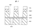
- FIG. 3 is a fragmentary cross-sectional view of the semiconductor device during a manufacturing step following that of FIG. 2;
- FIG. 4 is a fragmentary cross-sectional view of the semiconductor device during a manufacturing step following that of FIG. 3;
- FIG. 5 is a fragmentary cross-sectional view of the semiconductor device during a manufacturing step following that of FIG. 4;
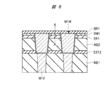
- 6 is a fragmentary cross-sectional view of the semiconductor device during a manufacturing step following that of FIG. 5;
- FIG. 6 is a CN-intensity distribution diagram of an interlayer insulating film of a semiconductor device according to an embodiment;
- FIG. 7 is an essential part cross sectional view of the semiconductor device during a manufacturing step following FIG. 6;
- FIG. 9 is an essential part cross sectional view of the semiconductor device during a manufacturing step following FIG. 8;
- FIG. 10 is an essential part cross sectional view of the semiconductor device during a manufacturing step following FIG. 9;
- FIG. 11 is an essential part cross sectional view of the semiconductor device during a manufacturing step following FIG. 10;
- FIG. 12 is a fragmentary cross-sectional view of the semiconductor device during a manufacturing step following that of FIG. 11;
- FIG. 13 is a fragmentary cross-sectional view of the semiconductor device during a manufacturing step following that of FIG.
- FIG. 12; 6 is a graph showing the relationship between the CN-strength ratio of the interlayer insulating film and the TDDB life of the semiconductor device of one embodiment. It is a gas flow figure concerning the manufacturing method of the semiconductor device of a 2nd embodiment. 6 is a CN-intensity distribution diagram of an interlayer insulating film according to a second embodiment. FIG. It is a modification of the gas flow figure concerning the manufacturing method of the semiconductor device of a 2nd embodiment.
- FIG. 10 is a CN-intensity distribution diagram of an interlayer insulating film according to a third embodiment. It is principal part sectional drawing of the semiconductor device which concerns on 4th Embodiment. FIG.
- FIG. 10 is a CN-intensity distribution diagram of an insulating barrier film according to a fourth embodiment. It is a gas flow figure concerning the manufacturing method of the semiconductor device of a 4th embodiment. It is a modification of the CN-intensity distribution diagram of the insulating barrier film according to the fourth embodiment.
- hatching may be omitted even in a cross-sectional view for easy understanding of the drawings. Further, even a plan view may be hatched to make the drawing easy to see.
- FIG. 1 is a principal cross-sectional view showing a cross-sectional structure of the semiconductor device of the present embodiment.
- a plurality of P-type well regions PW and a plurality of N-type well regions NW are formed on the main surface (front surface) of the P-type semiconductor substrate SUB made of silicon.
- An N-type MISFET (MetalNInsulator Semiconductor Field Effect Transistor) Qn (hereinafter referred to as N-type MISFETQn) is formed in the P-type well region PW, and a P-type MISFET Qp (hereinafter referred to as N-type well region NW).
- P-type MISFET Qp is formed.
- An element isolation film (element isolation region) ST made of an insulating film such as a silicon oxide film is partially formed on the surface of the semiconductor substrate SUB.
- the element isolation film ST defines an N-type MISFET formation region and a P-type MISFET formation region in the P-type well region PW and the N-type well region NW. That is, one or more N-type MISFETs are formed in a region surrounded by the element isolation film ST in the P-type well region PW in plan view. In plan view, one or more P-type MISFETs Qp are formed in a region surrounded by the element isolation film ST in the N-type well region NW.
- the N-type MISFET Qn includes an N-type source region NSD and an N-type drain region NSD in contact with the element isolation film ST, a channel formation region NCH between the source region NSD and the drain region NSD, and a gate insulation on the channel formation region NCH.
- the gate electrode NG is formed through the film NGI.
- a silicide film SIL is formed on the surfaces of the N-type source region NSD, the N-type drain region NSD, and the gate electrode NG.
- the P-type MISFET Qp includes a P-type source region PSD and a P-type drain region PSD that are in contact with the element isolation film ST, a channel formation region PCH between the source region PSD and the drain region PSD, and a gate insulation on the channel formation region PCH.
- the gate electrode PG is formed through the film PGI.
- a silicide film SIL is formed on the surfaces of the P-type source region PSD, the P-type drain region PSD, and the gate electrode PG.
- the N-type MISFET Qn, the P-type MISFET Qp, and the element isolation film ST are covered with a first etching stopper film EST1, which is an insulating film made of a silicon nitride film. Further, a first interlayer insulating film INS1 that is an insulating film is formed on the first etching stopper film EST1, and the first interlayer insulating film INS1 is made of a BP (Boron, Phosphorus) -TEOS film.
- BP Bion, Phosphorus
- a plurality of first contact holes VG1 are formed in the first etching stopper film EST1 and the first interlayer insulating film INS1, and a first plug electrode M1V that is a metal conductor film is provided in the first contact hole VG1. ing.
- the first plug electrode M1V is electrically connected to the source region NSD and drain region NSD of the N-type MISFET Qn, and further to the source region PSD and drain region PSD of the P-type MISFET Qp.
- the first plug electrode M1V has a laminated structure of a titanium nitride film (TiN) and a tungsten film (W).
- the first etching stopper film EST1 functions as an etching stopper when the first contact hole VG1 is formed in the first interlayer insulating film INS1. Etching at the time of forming the first contact hole VG1 is performed in the first contact hole VG1 in the first interlayer insulating film INS1 under the condition that the etching rate of the first interlayer insulating film INS1 is larger than the etching rate of the first etching stopper film EST1. Etching is performed to form. Next, by performing etching for forming the first contact hole VG1 in the first etching stopper EST1 whose thickness is smaller than that of the first interlayer insulating film INS1, it is possible to reduce the chipping of the semiconductor substrate SUB.
- a second etching stopper film EST2 that is an insulating film and a second interlayer insulating film INS2 that is an insulating film are sequentially formed.
- the second etching stopper film EST2 is made of a silicon nitride film
- the second interlayer insulating film INS2 is made of, for example, a low-k insulating film having a dielectric constant of 3.0 or less.
- the second interlayer insulating film INS2 is SiCOH, and other films include organic polymer films (polyarylene, benzocyclobutene, polyimide, etc.), parylene (registered trademark), or BCN (boron nitride carbon). A membrane or the like.
- a plurality of first wiring grooves WG1 are provided in the second etching stopper film EST2 and the second interlayer insulating film INS2, and a first wiring M1W made of a metal conductor film is formed in the first wiring groove WG1. ing.
- the first wiring M1W is a copper having a laminated structure of one or a plurality of laminated films of titanium (Ti), titanium nitride (TiN) film, tantalum (Ta) film, and tantalum nitride (TaN) film and a copper (Cu) film.
- Ti titanium
- TiN titanium nitride
- Ta tantalum
- TaN tantalum nitride
- Cu copper
- Wiring The copper film contains copper as a main component, but may contain additives such as aluminum (Al), manganese (Mn), or palladium (Pd).
- One or more laminated films of titanium (Ti), titanium nitride (TiN) film, tantalum (Ta) film, and tantalum nitride (TaN) film are formed between the copper (Cu) film and the second interlayer insulating film INS2. And has a role of preventing copper (Cu) from diffusing into the second interlayer insulating film INS2. That is, the above-described conductive barrier film.
- the first wiring M1W is electrically connected to the first plug electrode M1V.
- a first insulating barrier film BR1 that is an insulating film and a third interlayer insulating film INS3 that is an insulating film are sequentially formed so as to cover the first wiring M1W and the second interlayer insulating film INS2.
- the first insulating barrier film BR1 is made of a silicon nitride film, a silicon nitride thin film (SiCN thin film), or a laminated film thereof.
- the first insulating barrier film BR1 serves to prevent copper (Cu) constituting the first wiring M1W from diffusing into the third interlayer insulating film INS3. That is, the above-described insulating barrier film.
- the third interlayer insulating film INS3 is made of the same material as that of the second interlayer insulating film INS2, and is made of, for example, SiCOH.
- a plurality of second wiring grooves WG2 are provided in the third interlayer insulating film INS3, and a second wiring M2W made of a metal conductor film is formed in the second wiring groove WG2.
- a second contact hole VG2 is formed in the third interlayer insulating film INS3 and the first barrier film BR1 so as to be connected to the first wiring groove WG1, and the second contact hole VG2 is made of a metal conductor film.
- a second plug electrode M2V is provided.
- the second wiring M2W and the second plug electrode M2V include one or more laminated films of a titanium (Ti) film, a titanium nitride (TiN) film, a tantalum (Ta) film, and a tantalum nitride (TaN) film, and a copper (Cu) film. It is comprised integrally by the copper (Cu) wiring which consists of these laminated structures.
- One or more laminated films of titanium (Ti), titanium nitride (TiN) film, tantalum (Ta) film, and tantalum nitride (TaN) film are formed between the copper (Cu) film and the third interlayer insulating film INS3.
- the copper film contains copper as a main component, but may contain additives such as aluminum (Al), manganese (Mn), or palladium (Pd).
- the second wiring M2W is electrically connected to the first wiring M1W through the second plug electrode M2V.
- a second insulating barrier film BR2 that is an insulating film is formed so as to cover the second wiring M2W and the third interlayer insulating film INS3.
- the second insulating barrier film BR2 is composed of a single layer film or a laminated film of a silicon nitride film and a silicon nitride carbide thin film (SiCN thin film).
- first wiring M1W that is the first layer wiring and the second wiring M2W that is the second layer wiring are shown, but even if a further wiring is formed on the second wiring M2W, good.
- FIGS. 2 to 6 and FIGS. 8 to 13 are cross-sectional views of the main part in the manufacturing process of the semiconductor device of the present embodiment.
- FIG. 7 is a CN-intensity depth profile diagram of time-of-flight secondary ion mass spectrometry (TOF-SIMS) of a SiN / SiCOH stacked structure
- FIG. 14 is a SiCOH of TOF-SIMS.
- 6 is a graph showing a relationship between a ratio of a CN-strength bulk of a film and a SiCOH surface layer portion in the vicinity of SiN and an actual TDDB lifetime between the same layer wirings.
- FIG. 2 is a diagram illustrating a process of forming the second interlayer insulating film INS2 and the first insulating film INS21.
- a semiconductor substrate SUB on which an N-type MISFET Qn and a P-type MISFET Qp are formed is prepared, and a first interlayer insulating film INS1 made of an insulating film is formed on the semiconductor substrate SUB so as to cover the N-type MISFET Qn and the P-type MISFET Qp.
- a first contact hole VG1 is formed in the first interlayer insulating film INS1 so as to expose the source region NSD and drain region NSD of the N-type MISFET Qn, and further the source region PSD and drain region PSD of the P-type MISFET Qp.
- the first plug electrode M1V is formed in the first contact hole VG1.
- a second etching stopper EST2 made of an insulating film, a second interlayer insulating film INS2 made of an insulating film, and an insulating film are sequentially formed on the first plug electrode M1V and the first interlayer insulating film INS1.
- a first insulating film INS21 made of is formed.
- the SiCOH film constituting the second interlayer insulating film INS2 is composed of organic silane gas (3MS: trimethylsilane, 4MS: tetramethylsilane, 1MS: monomethylsilane, 2MS: dimethylsilane) and oxidizing gas (O2, N2O, CO, CO2, etc.) It can be formed by a CVD method using
- the first insulating film INS21 is a film having a higher dielectric constant and higher mechanical strength than the second interlayer insulating film INS2.
- the first insulating film INS21 has a higher dielectric resistance than the silicon oxide film or the second interlayer insulating film INS2 and has excellent processing resistance.
- a SiCOH film can be used.
- the film thickness of the first insulating film INS21 is smaller than the film thickness of the second interlayer insulating film INS2.
- FIG. 3 is a diagram illustrating a process of forming the first wiring groove WG1.
- a first resist film PR1 made of an insulating film having an opening corresponding to the pattern of the first wiring M1W is formed on the first insulating film INS21.
- the first resist film PR1 as a mask, the first insulating film INS21 and the second interlayer insulating film INS2 are dry-etched to form the first wiring groove WG1. This dry etching is performed under conditions where the etching rates of the second interlayer insulating film INS2 and the first insulating film INS21 are high (large) with respect to the second etching stopper film EST2.
- the first wiring trench WG1 is formed not only in the second interlayer insulating film INS2 but also in the first insulating film INS21. Further, the cross-sectional shape of the first wiring groove WG1 is a tapered shape in which the opening diameter of the upper portion of the first wiring groove WG1 is wider than the opening diameter of the bottom portion of the first wiring groove WG1. That is, the width of the first insulating film INS21 and the second interlayer insulating film INS2 between the adjacent first wiring trenches WG1 is narrower at the top than at the bottom.
- FIG. 4 is a diagram illustrating a process of forming the first wiring M1W.
- the first resist film PR1 is removed, and then the second etching stopper film EST2 is etched by the entire surface etch back to expose the upper surface of the first plug electrode M1V.
- a first conductive barrier film CBR1 which is a conductive film and a first copper film CU1 which is a conductive film are sequentially formed in the first wiring trench WG1, and then a CMP process is performed on the surface of the semiconductor substrate SUB.
- the first conductive barrier film CBR1 and the first copper film CU1 are selectively left only in the first wiring trench WG1, and the first conductive barrier film CBR1 and the first copper film CU1 on the second interlayer insulating film INS2 are left.
- the first wiring M1W is formed by removing. In this CMP process, the first insulating film INS21 is also removed, and the structure shown in FIG. 4 is obtained.
- the adjacent first wirings M1W are electrically separated by the Low-k insulating film, and therefore between the first wirings M1W. The capacity can be reduced.
- FIG. 5 is a drawing for explaining the steps of the ammonia plasma treatment.
- Plasma treatment containing ammonia (NH 3) gas is performed on the surfaces of the first wiring M 1 W and the second interlayer insulating film INS 2.
- the ammonia plasma treatment is performed using NH 3 gas under the conditions of pressure: 1.0 to 8.0 Torr, high frequency power: 50 W to 500 W, and time: 3 Sec to 100 Sec.
- N2 gas may be added to NH3 gas.
- the oxide film (CuO) formed on the surface of the first copper film CU1 constituting the first wiring M1W in the CMP process is removed, and the surface of the second interlayer insulating film INS2 is modified (for example, , Fill dangling bonds).
- the adhesion (adhesion) between the first insulating barrier film BR1 and the first wiring M1W formed in the next step can be improved.
- the second interlayer insulating film INS2 is composed of a low-k film
- the first damage layer DM1 is formed on the surface of the second interlayer insulating film INS2 by this ammonia plasma treatment.
- the first damaged layer DM1 is formed in a range of 4 nm from the surface of the second interlayer insulating film INS2.
- the first damage layer DM1 is a film obtained by nitriding the SiCOH film constituting the second interlayer insulating film INS2.
- the first electric field relaxation layer ER1 is formed below the first damage layer DM1 by ammonia plasma treatment.
- the first electric field relaxation layer ER1 is also a film obtained by nitriding the SiCOH film constituting the second interlayer insulating film INS2. That is, the first damage layer DM1 and the first electric field relaxation layer ER1 are regions having a higher nitrogen concentration than the second interlayer insulating film INS2.
- the first damage layer DM1 and the first electric field relaxation layer ER1 are divided into regions, but actually both are integrated.
- FIG. 6 is a drawing for explaining a process of forming the first insulating barrier film BR1.
- a first insulating barrier film BR1 made of an insulating film is formed so as to cover the surface of the first wiring M1W and the surface of the second interlayer insulating film INS2 from which the oxide film (CuO) has been removed by the ammonia plasma treatment.
- FIG. 7 is a graph showing the CN-intensity (nitrogen concentration) distribution by TOF-SIMS assuming the AA portion of FIG. This is a result of analysis from the first insulating barrier film BR1 to a predetermined depth of the second interlayer insulating film INS2 by the TOF-SIMS method, and the nitrogen concentration is expressed using CN-intensity.
- the nitrogen concentration in the depth direction of the second interlayer insulating film INS2 has a concentration peak at a position deeper than the surface. The concentration peak is located in the range of 5 nm to 20 nm from the surface of the second interlayer insulating film INS2.
- a surface portion (0 to 4 nm) of the second interlayer insulating film INS2 is the first damage layer DM1, and a region having a nitrogen concentration higher than the nitrogen concentration of the surface portion is the first electric field relaxation layer ER1.
- the first electric field relaxation layer ER1 there are a region where the nitrogen concentration gradually increases, a peak region of the nitrogen concentration, and a region where the nitrogen concentration gradually decreases.
- the nitrogen concentration of the first electric field relaxation layer ER1 is higher than the nitrogen concentration of the first damage layer DM1.
- the dielectric constant of the first electric field relaxation layer ER1 is higher than the dielectric constant of the first damage layer DM1.
- the second interlayer insulating film INS2 by providing a region (layer) having a dielectric constant higher than the surface dielectric constant at a position deeper than the surface (upper surface) of the second interlayer insulating film INS2 between the adjacent first wirings M1W.
- the electric field on the surface of the second interlayer insulating film INS2 can be relaxed.
- the TDDB characteristic (lifetime) between the adjacent first wirings M1W can be improved.
- the nitrogen concentration peak position of the first electric field relaxation layer ER1 is 1 of the thickness of the first wiring M1W. Shallow than / 2.
- FIG. 8 is a diagram illustrating a process of forming the third interlayer insulating film INS3, the second insulating film INS31, and the second contact hole VG2.
- a third interlayer insulating film INS3 and a second insulating film INS31 are sequentially formed on the first insulating barrier film BR1.
- the third interlayer insulating film INS3 and the second insulating film INS31 are composed of films similar to the second interlayer insulating film INS2 and the first insulating film INS21.
- a second resist film PR2 made of an insulating film having an opening corresponding to the second contact hole VG2 is formed on the second insulating film INS31. As shown in FIG.
- the second insulating film INS31 and the third interlayer insulating film INS3 are dry-etched to form the second contact hole VG2. Etching is stopped on the first insulating barrier film BR1. Therefore, the first insulating barrier film BR1 remains at the bottom of the second contact hole VG2.
- FIG. 9 is a drawing for explaining the formation process of the fourth resist film PR4 made of an insulating film for forming the second wiring trench WG2.
- a third resist film PR3 is formed in the second contact hole VG2 and on the second insulating film INS31.
- a third insulating film INS32 and an antireflection film BARC made of an insulating film are formed on the third resist film PR3.
- the third insulating film INS32 is made of a silicon oxide film and is formed by a low temperature CVD method.
- a fourth resist film PR4 having an opening corresponding to the second wiring groove WG2 is formed on the antireflection film BARC.
- FIG. 10 is a diagram illustrating a process of forming the second wiring groove WG2.
- the second insulating film INS31 and the third interlayer insulating film INS3 are dry-etched to form the second wiring groove WG2.
- the third insulating film INS32, the antireflection film BARC, and the fourth resist film PR4 formed above the third resist film PR3 are removed at the same time, and as shown in FIG. 10, the periphery of the second wiring groove WG2
- the third resist film PR3 remains in the second contact hole VG2.
- FIG. 11 is a diagram illustrating a process of removing the first barrier film BR1.
- the third resist film PR3 remaining around the second wiring trench WG2 and in the second contact hole VG2 is removed, and then the entire surface is etched back in order to remove the opening of BR1, thereby obtaining the structure shown in FIG. As shown, the surface of the first wiring M1W is exposed. In the entire etch back process, the second insulating film 31 is also etched and thinned.
- FIG. 12 is a diagram illustrating a process of forming the second wiring M2W.
- a second conductive barrier film CBR2 which is a conductive film and a second copper film CU2 which is a conductive film are sequentially formed in the second contact hole VG2 and the second wiring groove WG2, and then formed on the surface of the second copper film CU2.
- a CMP process is performed. Then, the second conductive barrier film CBR2 and the second copper film CU2 are selectively left only in the second contact hole VG2 and the second wiring trench WG2, thereby forming the second wiring M2W.
- the second insulating film INS31 is also removed and the surface of the third interlayer insulating film INS3 is exposed, so that the second wiring M2W is electrically separated by the Low-k insulating film.
- the capacitance between the two wirings M2W can be reduced.
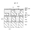
- FIG. 13 is a drawing for explaining the ammonia plasma treatment process and the formation process of the second insulating barrier film BR2.
- Plasma treatment containing ammonia (NH 3) gas is performed on the surfaces of the second wiring M 2 W and the third interlayer insulating film INS 3.
- the conditions for the ammonia plasma treatment are the same as those for the first wiring M1W.
- a second damage layer DM2 is formed on the surface of the third interlayer insulating film INS3.
- the second damage layer DM2 is formed in a range of 4 nm from the surface of the third interlayer insulating film INS3.
- the second damage layer DM2 is a film obtained by nitriding the SiCOH film constituting the third interlayer insulating film INS3.
- the second electric field relaxation layer ER2 is formed below the second damage layer DM2 by ammonia plasma treatment.
- the second electric field relaxation layer ER2 is also a film obtained by nitriding the SiCOH film constituting the third interlayer insulating film INS3. That is, the second damage layer DM2 and the second electric field relaxation layer ER2 are regions having a higher nitrogen concentration than the third interlayer insulating film INS3.
- the second damage layer DM2 and the second electric field relaxation layer ER2 are divided into regions, but in reality, both are integrated.
- a second insulating barrier film BR2 made of an insulating film is formed so as to cover the third interlayer insulating film INS3 and the second wiring M2W, and the structure of FIG. 13 is obtained.
- the nitrogen concentration distribution in the BB portion of FIG. 13 is the same as the graph shown in FIG. Since the second electric field relaxation layer ER2 has the same configuration as the first electric field relaxation layer ER1, the second electric field relaxation layer ER2 has the same effect as the first electric field relaxation layer ER1. Although redundant description is omitted, the description in the explanatory paragraph of FIG.
- the second interlayer insulating film INS2 is changed to the third interlayer insulating film INS3, the first damaged layer DM1 is changed to the second damaged layer DM2, and the second damaged layer DM2 is changed to the second damaged layer DM2. It is possible to read by replacing the first electric field relaxation layer ER1 with the second electric field relaxation layer ER2 and the first wiring M1W with the second wiring M2W.
- FIG. 14 is a graph for explaining the effect of the present embodiment.
- FIG. 14 shows the relationship between the CN-strength ratio (nitrogen concentration ratio) and the TDDB lifetime in the inside and on the surface of the SiCOH film constituting the interlayer insulating film.
- the CN-intensity ratio is 1 or more
- the TDDB life is improved by an order of magnitude or more. That is, by providing a layer having a nitrogen concentration higher than the surface nitrogen concentration inside the interlayer insulating film, the TDDB life is improved by one digit or more.
- the TDDB life between the adjacent first wirings M1W is improved by one digit or more.
- the second electric field relaxation layer ER2 the TDDB life between the adjacent second wirings M2W is improved by one digit or more.
- the second embodiment is a modification of the first embodiment, and differs from the first embodiment in the formation method of the first electric field relaxation layer ER1 and the second electric field relaxation layer ER2 and the conditions of the ammonia plasma treatment.
- the other parts are the same.
- the first electric field relaxation layer ER1 is formed during the formation process of the second interlayer insulating film INS2
- the second electric field relaxation layer ER2 is formed during the formation of the third interlayer insulation film INS3. Therefore, the first damage layer DM1 and the second damage layer DM2 are formed in the ammonia plasma processing step, but the first electric field relaxation layer ER1 and the second electric field relaxation layer ER2 are not formed.
- FIG. 15 is a diagram showing a gas flow when forming the second interlayer insulating film INS2 and the third interlayer insulating film INS3, and FIG. 16 is a flight time of the AA portion of FIG. 6 and the BB portion of FIG. It is a graph which shows CN intensity
- TOF-SIMS secondary ion mass spectrometer
- the SiCOH film constituting the second interlayer insulating film INS2 is composed of organic silane gas (3MS: trimethylsilane, 4MS: tetramethylsilane, 1MS: monomethylsilane, 2MS: dimethylsilane) and oxidizing gas (O2, N2O, CO, CO2, etc.) It is formed by the CVD method using The second embodiment is characterized in that a gas containing nitrogen (N2, NH3, etc.) is added at a predetermined timing. Other CVD conditions are in the range of 300 to 400 ° C., the pressure is in the range of 1.0 to 8.0 Torr, and the high frequency power is in the range of 100 W to 500 W. As shown in FIG.
- an organosilane gas and oxygen (O 2) gas are allowed to flow and power is simultaneously applied.
- ammonia (NH 3) gas is added to slowly increase the flow rate, and when it reaches the set value, it is slowly decreased to zero.
- an organosilane gas and oxygen (O2) gas are flowed, and at the same time, the power is turned off.
- the nitrogen concentration in the film can be made gradation.
- the second electric field relaxation layer ER2 can be formed deeper than the surface of the third interlayer insulating film INS3 when the third interlayer insulating film INS3 is formed.
- the conditions of the ammonia plasma treatment for the surfaces of the second interlayer insulating film INS2 and the third interlayer insulating film INS3 are different from those in the first embodiment.
- the first damage layer DM1 and the second damage layer DM2 generated by the ammonia plasma treatment have a lower nitrogen concentration than the electric field relaxation layers ER1 and ER2 when forming the second interlayer insulating film INS2 and the third interlayer insulating film INS3. Better. For example, it is desirable to add hydrogen gas during ammonia plasma treatment.
- FIG. 16 shows the CN-intensity (nitrogen concentration) of the AA portion of FIG. 6 and the BB portion of FIG. 13 obtained by the second embodiment.
- the AA portion in FIG. 6 will be described as an example, but the same effect can be obtained in the BB portion in FIG.
- the first electric field relaxation layer ER1 includes a region where the nitrogen concentration gradually increases, a peak region of the nitrogen concentration, and a region where the nitrogen concentration gradually decreases.
- the nitrogen concentration of the first electric field relaxation layer ER1 is higher than the nitrogen concentration of the first damage layer DM1.
- the dielectric constant of the first electric field relaxation layer ER1 is higher than the dielectric constant of the first damage layer DM1.
- the first electric field relaxation layer ER1 is formed in a separate process from the first damage layer DM1, damage due to the ammonia plasma treatment on the surface of the second interlayer insulating film INS2 can be reduced.
- the TDDB life between one wiring M1W can be improved.
- the fact that the nitrogen concentration has a peak deeper than the interface between the first insulating barrier film BR1 and the second interlayer insulating film INS2 means that the dielectric constant increases, and the electric field increases between the first insulating barrier film BR1 and the second interlayer insulating film. This means that there is no concentration at the interface of the film INS2.
- the inter-wiring TDDB can be improved.
- FIG. 17 is a drawing showing a gas flow which is a modification of the method for forming the second interlayer insulating film INS2 in the second embodiment.
- the present invention can also be applied to the third interlayer insulating film INS3. It is characterized in that the flow rate of O 2 gas is changed instead of adding ammonia gas.
- an organosilane gas and oxygen (O 2) gas are allowed to flow, and at the same time, high frequency power is applied.
- the oxygen (O 2) gas flow rate is further slowly increased, and when it reaches the set value, it is slowly decreased to the original set value. Thereafter, the power is turned off simultaneously with the organosilane gas and oxygen (O2) gas.
- the oxygen concentration in the film can be made gradation.
- the first electric field relaxation layer ER1 can be formed at a position deeper than the surface of the second interlayer insulating film INS2.
- This manufacturing method can also be applied to the third interlayer insulating film INS3.
- a semiconductor device having the structure of FIG. 13 of the first embodiment can be formed.
- the first electric field relaxation layer ER1 is different from the first embodiment in that it is composed of a layer having an oxygen concentration higher than that of the second interlayer insulating film INS2.
- the dielectric constant of the first electric field relaxation layer ER1 is higher than the dielectric constant of the second interlayer insulating film INS2, the dielectric constant higher than the dielectric constant of the second interlayer insulating film INS2 is located deeper than the surface of the second interlayer insulating film INS2.
- the oxygen concentration peak position of the first electric field relaxation layer ER1 is preferably shallower than 1/2 of the thickness of the first wiring M1W.
- the oxygen concentration peak position of the second electric field relaxation layer ER2 is preferably shallower than 1/2 of the thickness of the second wiring M2W.
- the third embodiment is a modification of the second embodiment, and differs from the second embodiment in the formation method of the first electric field relaxation layer ER1 and the second electric field relaxation layer ER2, and the other parts are the same. is there.
- the first electric field relaxation layer ER1 is formed after the formation process of the second interlayer insulating film INS2
- the second electric field relaxation layer ER2 is formed after the formation of the third interlayer insulation film INS3.
- FIG. 18 is a graph showing the CN-intensity (nitrogen concentration) distribution by the time-of-flight secondary ion mass spectrometer (TOF-SIMS) in the AA part of FIG. 6 and the BB part of FIG.
- the first electric field relaxation layer ER1 having a nitrogen concentration higher than the nitrogen concentration of the first damage layer DM1 exists at a position deeper than the first damage layer DM1 on the surface of the second interlayer insulating film INS2.
- a peak portion of nitrogen concentration exists in the first electric field relaxation layer ER1.
- Embodiment 2 there is an advantage that the depth direction and concentration control of nitrogen element are excellent. Similar effects can be obtained in the BB portion of FIG.
- the fourth embodiment is a modification of the first embodiment, and has the following differences.
- the first insulating barrier film BR1 is composed of the first sub-insulating barrier film BR11 and the second sub-insulating barrier film BR12
- the second insulating barrier film BR2 is the first sub-insulating barrier film BR21.
- a second sub-insulating barrier film BR22 is the first electric field relaxation layer ER1 in the second interlayer insulating film INS2 and the second electric field relaxation layer 2 in the third electric field relaxation layer INS3 are not formed.
- FIG. 19 shows a cross-sectional structure of a main part of the semiconductor device according to the fourth embodiment.
- the first insulating barrier film BR1 covering the first wiring M1W.
- the first insulating barrier film BR1 includes a first sub-insulating barrier layer BR11 that covers the first wiring M1W, and a second sub-insulating barrier layer BR12 formed on the first sub-insulating barrier layer BR11. ing.
- the second sub-insulating barrier layer BR12 has a nitrogen concentration higher than that of the first sub-insulating barrier layer BR11.
- the second sub-insulating barrier layer BR12 has a nitrogen concentration higher than the nitrogen concentration on the lower surface (interface with the first wiring M1W) of the first sub-insulating barrier layer BR11.
- the first sub-insulating barrier layer BR11 and the second sub-insulating barrier layer BR12 are divided into regions, but actually both are integrated.
- FIG. 20 is a graph showing the CN-intensity (nitrogen concentration) distribution by the time-of-flight secondary ion mass spectrometer (TOF-SIMS) in the AA portion of FIG.
- the first insulating barrier film at a position farther from the interface than the nitrogen concentration at the interface between the second interlayer insulating film INS2 positioned between the first wires M1W and the first insulating barrier film BR1 formed thereon.
- the nitrogen concentration of BR1 is high. That is, the second sub-insulating barrier layer BR12 exists at a position away from the interface.
- the nitrogen concentration of the first insulating barrier film BR1 increases as the distance from the interface between the second interlayer insulating film INS2 and the first insulating barrier film BR1 formed thereon increases.
- a SiCN film is used as the first insulating barrier film BR1.
- the SiCN film is formed by, for example, the CVD method, and the temperature is in the range of 300 to 400 ° C., the pressure is in the range of 1.0 to 8.0 Torr, and the high frequency power is in the range of 50 to 1000 W.
- the gas organosilane, SiH4, ammonia (NH3), CO, CO2, N2O, or the like is used.
- FIG. 21 is a gas flow diagram when forming the SiCN film constituting the first insulating barrier film BR1 using the organic silane gas and the ammonia (NH 3) gas.
- an organosilane gas and ammonia (NH 3) gas are allowed to flow, and power is simultaneously applied.
- the ammonia (NH 3) gas is gradually increased in its original flow rate, and slowly lowered to the original set value when the set value is reached. Thereafter, the organosilane gas, ammonia (NH 3) gas, and power are turned off simultaneously.
- the nitrogen concentration in the first insulating barrier film BR 1 can be made gradation.
- the nitrogen concentration of BR1 By increasing the nitrogen concentration of BR1, the TDDB life between adjacent first wirings M1W can be improved. This is because the electric field between the adjacent first wirings M1W in the interface portion can be relaxed by providing a region having a high nitrogen concentration in the first insulating barrier film BR1 at a position away from the interface.
- FIG. 22 is a graph showing the CN-intensity (nitrogen concentration) distribution by the time-of-flight secondary ion mass spectrometer (TOF-SIMS) in the AA portion of FIG. It is a modification of the example demonstrated in FIG.
- a region having a peak of nitrogen concentration exists in the second sub-insulating barrier layer BR12 formed on the first sub-insulating barrier layer BR11, and the peak of nitrogen concentration is the first insulating barrier film BR1.
- a structure having a nitrogen concentration peak in the range of 5 to 40 nm from the lower surface of the substrate is desirable.
- the second insulating barrier film BR2 has the same structure and the same effect. This structure is desirable because having a nitrogen concentration peak in one film is more resistant to fracture than if the interface has a peak.
- the invention made by the present inventor has been specifically described based on the embodiment.
- the invention is not limited to the embodiment, and various modifications can be made without departing from the scope of the invention.
- the embodiments can be appropriately combined.
- the fourth embodiment can be combined with the first to third embodiments.
- the present invention includes the following inventions.
- A a step of preparing a semiconductor substrate;
- B forming an interlayer insulating film having a first main surface and a predetermined film thickness on the semiconductor substrate;
- C forming a first wiring groove and a second wiring groove on the first main surface of the interlayer insulating film;
- D a step of selectively providing a copper film in the first wiring groove and the second wiring groove to form the first wiring and the second wiring;
- E performing a plasma treatment containing ammonia on the first main surface of the first wiring, the second wiring, and the interlayer insulating film;
- the nitrogen concentration of the damaged layer and the electric field relaxation layer is higher than the nitrogen concentration of the interlayer insulating film, and the nitrogen concentration of the electric field relaxation layer is higher than the nitrogen concentration of the damaged layer.
Landscapes
- Internal Circuitry In Semiconductor Integrated Circuit Devices (AREA)
- Physics & Mathematics (AREA)
- Engineering & Computer Science (AREA)
- Plasma & Fusion (AREA)
- Chemical & Material Sciences (AREA)
- Chemical Kinetics & Catalysis (AREA)
- Geometry (AREA)
- High Energy & Nuclear Physics (AREA)
Abstract
Description
図1は、本実施の形態の半導体装置の断面構造を示す要部断面図である。
本実施の形態2は、上記実施の形態1の変形例であり、実施の形態1とは、第1電界緩和層ER1および第2電界緩和層ER2の形成方法とアンモニアプラズマ処理の条件が異なり、その他の部分は同様である。本実施の形態2では、第1電界緩和層ER1は第2層間絶縁膜INS2の形成工程中に、第2電界緩和層ER2は第3層間絶縁膜INS3の形成中に形成される。従って、アンモニアプラズマ処理工程で第1ダメージ層DM1および第2ダメージ層DM2が形成されるが、第1電界緩和層ER1および第2電界緩和層ER2は形成されない。図15は、第2層間絶縁膜INS2および第3層間絶縁膜INS3形成時のガスフローを示す図面であり、図16は、図6のA-A部分および図13のB-B部分の飛行時間二次イオン質量分析計(TOF-SIMS)によるCN-強度(窒素濃度)分布を示すグラフである。
本実施の形態3は、上記実施の形態2の変形例であり、実施の形態2とは、第1電界緩和層ER1および第2電界緩和層ER2の形成方法が異なり、その他の部分は同様である。本実施の形態3では、第1電界緩和層ER1は第2層間絶縁膜INS2の形成工程後に、第2電界緩和層ER2は第3層間絶縁膜INS3の形成後に形成される。つまり、第2層間絶縁膜INS2を形成した後、第2層間絶縁膜INS2の表面から所定の深さに窒素のイオン打ち込みを実施することにより、第2層間絶縁膜INS2の表面より深い位置に第1電界緩和層ER1を形成するものである。第3層間絶縁膜INS3にも同様の方法を適用できる。
本実施の形態4は、上記実施の形態1の変形例であり、以下の相違点が有る。先ず、第1絶縁性バリヤ膜BR1が第1サブ絶縁性バリヤ膜BR11と第2サブ絶縁性バリヤ膜BR12とで構成されており、第2絶縁性バリヤ膜BR2が第1サブ絶縁性バリヤ膜BR21と第2サブ絶縁性バリヤ膜BR22とで構成されている。第2層間絶縁膜INS2内の第1電界緩和層ER1および第3電界緩和層INS3内の第2電界緩和層2は形成されていない。
(a)半導体基板を準備する工程、
(b)前記半導体基板上に、第1主面を有し、かつ所定の膜厚を有する層間絶縁膜を形成する工程、
(c)前記層間絶縁膜の前記第1主面に第1配線溝および第2配線溝を形成する工程、
(d)前記第1配線溝および第2配線溝内に選択的に銅膜を設け、第1配線および第2配線を形成する工程、
(e)前記第1配線、前記第2配線および前記層間絶縁膜の前記第1主面にアンモニアを含有するプラズマ処理を施す工程、
を有し、
前記工程(e)において、前記層間絶縁膜の前記第1主面にはダメージ層が形成され、前記ダメージ層の下方には電界緩和層が形成され、
前記ダメージ層および前記電界緩和層の窒素濃度は、前記層間絶縁膜の窒素濃度よりも大であり、前記電界緩和層の窒素濃度は前記ダメージ層の窒素濃度よりも大である、半導体装置の製造方法。
BR1,BR2 絶縁性バリヤ膜
BR11,BR12,BR21,BR22 サブ絶縁性バリヤ層
CU1,CU2 銅膜
CBR1,CBR2 導電性バリヤ膜
DM1,DM2 ダメージ層
ER1,ER2 電界緩和層
EST1,EST2 エッチングストッパ膜
INS1,INS2,INS3 層間絶縁膜
INS21,INS31,INS32 絶縁膜
M1W,M2W 配線
M1V,M2V プラグ電極
NCH,PCH チャネル領域
NG,PG ゲート電極
NGI,PGI ゲート絶縁膜
NSD,PSD ソース領域またはドレイン領域
NW N型ウエル領域
PR1,PR2,PR3,PR4 レジスト膜
PW P型ウエル領域
Qn N型MISFET
Qp P型MISFET
SUB P型半導体基板
SIL シリサイド膜
ST 素子分離膜
VG1,VG2 コンタクトホール
WG1,WG2 配線溝
Claims (20)
- 半導体基板と、
前記半導体基板上に形成され、主面を有する層間絶縁膜と、
前記層間絶縁膜内に埋め込まれ、互いに隣接する第1配線および第2配線と、
前記第1配線と前記第2配線との間に位置し、前記層間絶縁膜の前記主面に形成されたダメージ層と、
前記ダメージ層の下方において、前記層間絶縁膜に形成された電界緩和層と、
を有し、
前記第1配線と前記第2配線とは、主に銅膜からなり、
前記ダメージ層と前記電界緩和層とは、窒素を含む層であり、前記電界緩和層の窒素濃度は、前記ダメージ層の窒素濃度よりも大である、半導体装置。 - 請求項1記載の半導体装置において、
前記層間絶縁膜は、誘電率が3.0以下の絶縁膜からなる、半導体装置。 - 請求項2記載の半導体装置において、
前記層間絶縁膜は、SiCOH膜からなる、半導体装置。 - 請求項1記載の半導体装置において、
前記ダメージ層は、前記層間絶縁膜の前記主面から深さ4nmの範囲に存在する、半導体装置。 - 請求項1記載の半導体装置において、
前記電界緩和層は、窒素濃度のピーク領域を有する、半導体装置。 - 請求項5記載の半導体装置において、
前記窒素濃度のピーク領域は、前記層間絶縁膜の前記主面から5~20nmの範囲に位置する、半導体装置。 - 請求項1記載の半導体装置において、
前記電界緩和層は、前記層間絶縁膜の前記主面を基準にして、前記第1配線の厚さの1/2より浅い位置に設けられている、半導体装置。 - 半導体基板と、
前記半導体基板上に形成され、第1主面を有する層間絶縁膜と、
前記層間絶縁膜内に埋め込まれ、互いに隣接する第1配線および第2配線と、
前記第1配線と前記第2配線との間に位置し、前記層間絶縁膜の前記第1主面に形成されたダメージ層と、
前記第1配線、前記第2配線およびダメージ層に接触し、前記第1配線、前記第2配線および前記層間絶縁膜を覆う絶縁性バリヤ膜と、
を有し、
前記第1配線と前記第2配線とは、主に銅膜からなり、
前記絶縁性バリヤ膜は、窒素を含有する絶縁膜であり、前記ダメージ層に接触する第1表面と前記第1表面と反対側の第2表面とを有し、前記絶縁性バリヤ膜は、前記第1表面の窒素濃度よりも高い窒素濃度を有する第1領域を有する、半導体装置。 - 請求項8記載の半導体装置において、
前記窒素濃度が高い第1領域は、前記第2表面側に位置する、半導体装置。 - 請求項8記載の半導体装置において、
前記絶縁性バリヤ膜の窒素濃度は、前記第1表面から前記第2表面に向かって増加している、半導体装置。 - 請求項8記載の半導体装置において、
前記層間絶縁膜は、誘電率が3.0以下の絶縁膜からなる、半導体装置。 - 請求項11記載の半導体装置において、
前記層間絶縁膜は、SiCOH膜からなる、半導体装置。 - 請求項8記載の半導体装置において、
前記ダメージ層の下方において、前記層間絶縁膜内に電界緩和層を有する、半導体装置。 - 請求項13記載の半導体装置において、
前記ダメージ層と前記電界緩和層とは、窒素を含む層であり、前記電界緩和層の窒素濃度は、前記ダメージ層の窒素濃度よりも大である、半導体装置。 - (a)半導体基板を準備する工程、
(b)前記半導体基板上に、第1主面を有し、かつ所定の膜厚を有する層間絶縁膜を形成する工程、
(c)前記層間絶縁膜の前記第1主面に第1配線溝および第2配線溝を形成する工程、
(d)前記第1配線溝および第2配線溝内に選択的に銅膜を設け、第1配線および第2配線を形成する工程、
(e)前記第1配線、前記第2配線および前記層間絶縁膜の前記第1主面にアンモニアを含有するプラズマ処理を施す工程、
を有し、
前記工程(b)において、前記層間絶縁膜には、前記第1主面より深い位置に電界緩和層が設けられており、
前記工程(e)において、前記層間絶縁膜の前記第1主面にはダメージ層が形成される、半導体装置の製造方法。 - 請求項15記載の半導体装置の製造方法において、
前記電界緩和層と前記ダメージ層は、前記層間絶縁膜よりも窒素濃度が大の層である、半導体装置の製造方法。 - 請求項16記載の半導体装置の製造方法において、
前記電界緩和層は、前記層間絶縁膜を形成後に、前記層間絶縁膜内に窒素をイオン打ち込みすることにより形成する、半導体装置の製造方法。 - 請求項16記載の半導体装置の製造方法において、
前記層間絶縁膜はSiCOH膜からなり、前記SiCOH膜は、有機シランガスおよび酸化ガスを用いたCVD法により形成し、
前記SiCOH膜形成工程の途中でアンモニアガスを添加することにより、前記SiCOH膜内に前記電界緩和層を形成する、半導体装置の製造方法。 - 請求項15記載の半導体装置の製造方法において、
前記層間絶縁膜はSiCOH膜からなり、前記SiCOH膜は、有機シランガスおよび酸化ガスを用いたCVD法により形成し、
前記SiCOH膜形成工程の途中で酸素系ガスの流量を増加することにより、前記SiCOH膜内に前記電界緩和層を形成する、半導体装置の製造方法。 - 請求項15記載の半導体装置の製造方法において、
前記工程(e)の後に、更に、
(f)前記層間絶縁膜上に、前記第1配線、前記第2配線および前記ダメージ層に接する第1表面と前記第1表面と反対側の第2表面を有する絶縁性バリヤ膜を形成する工程、
を有し、
前記絶縁性バリヤ膜の前記第2表面の窒素濃度は、前記第1表面の窒素濃度よりも大である、半導体装置の製造方法。
Priority Applications (14)
| Application Number | Priority Date | Filing Date | Title |
|---|---|---|---|
| EP20213902.8A EP3809451B1 (en) | 2013-11-08 | 2013-11-08 | Semiconductor device |
| CN201380011034.4A CN104919576B (zh) | 2013-11-08 | 2013-11-08 | 半导体器件及其制造方法 |
| JP2014540661A JP6134727B2 (ja) | 2013-11-08 | 2013-11-08 | 半導体装置およびその製造方法 |
| CN202010792984.7A CN111952281B (zh) | 2013-11-08 | 2013-11-08 | 半导体器件及其制造方法 |
| PCT/JP2013/080195 WO2015068251A1 (ja) | 2013-11-08 | 2013-11-08 | 半導体装置およびその製造方法 |
| KR1020217038608A KR102480116B1 (ko) | 2013-11-08 | 2013-11-08 | 반도체 장치 및 그 제조 방법 |
| KR1020147022890A KR102186873B1 (ko) | 2013-11-08 | 2013-11-08 | 반도체 장치 및 그 제조 방법 |
| US14/381,572 US9281276B2 (en) | 2013-11-08 | 2013-11-08 | Semiconductor device and manufacturing method of the same |
| KR1020207034402A KR102332952B1 (ko) | 2013-11-08 | 2013-11-08 | 반도체 장치 및 그 제조 방법 |
| EP13874852.0A EP3067920B1 (en) | 2013-11-08 | 2013-11-08 | Semiconductor device |
| TW107134158A TWI669795B (zh) | 2013-11-08 | 2014-07-31 | Semiconductor device |
| TW103126295A TWI641098B (zh) | 2013-11-08 | 2014-07-31 | Semiconductor device and method of manufacturing same |
| US15/047,623 US9559052B2 (en) | 2013-11-08 | 2016-02-18 | Semiconductor device and manufacturing method of the same |
| US15/394,752 US20170110399A1 (en) | 2013-11-08 | 2016-12-29 | Semiconductor device and manufacturing method of the same |
Applications Claiming Priority (1)
| Application Number | Priority Date | Filing Date | Title |
|---|---|---|---|
| PCT/JP2013/080195 WO2015068251A1 (ja) | 2013-11-08 | 2013-11-08 | 半導体装置およびその製造方法 |
Related Child Applications (2)
| Application Number | Title | Priority Date | Filing Date |
|---|---|---|---|
| US14/381,572 A-371-Of-International US9281276B2 (en) | 2013-11-08 | 2013-11-08 | Semiconductor device and manufacturing method of the same |
| US15/047,623 Division US9559052B2 (en) | 2013-11-08 | 2016-02-18 | Semiconductor device and manufacturing method of the same |
Publications (1)
| Publication Number | Publication Date |
|---|---|
| WO2015068251A1 true WO2015068251A1 (ja) | 2015-05-14 |
Family
ID=53041053
Family Applications (1)
| Application Number | Title | Priority Date | Filing Date |
|---|---|---|---|
| PCT/JP2013/080195 Ceased WO2015068251A1 (ja) | 2013-11-08 | 2013-11-08 | 半導体装置およびその製造方法 |
Country Status (7)
| Country | Link |
|---|---|
| US (3) | US9281276B2 (ja) |
| EP (2) | EP3067920B1 (ja) |
| JP (1) | JP6134727B2 (ja) |
| KR (3) | KR102480116B1 (ja) |
| CN (2) | CN111952281B (ja) |
| TW (2) | TWI669795B (ja) |
| WO (1) | WO2015068251A1 (ja) |
Families Citing this family (16)
| Publication number | Priority date | Publication date | Assignee | Title |
|---|---|---|---|---|
| CN107275309B (zh) | 2011-12-20 | 2021-02-09 | 英特尔公司 | 保形低温密闭性电介质扩散屏障 |
| KR102480116B1 (ko) * | 2013-11-08 | 2022-12-23 | 르네사스 일렉트로닉스 가부시키가이샤 | 반도체 장치 및 그 제조 방법 |
| US9614045B2 (en) * | 2014-09-17 | 2017-04-04 | Infineon Technologies Ag | Method of processing a semiconductor device and chip package |
| US9859154B2 (en) * | 2016-03-11 | 2018-01-02 | Taiwan Semiconductor Manufacturing Co., Ltd. | Structure and formation method of interconnect structure of semiconductor device |
| US10269706B2 (en) * | 2016-07-26 | 2019-04-23 | Taiwan Semiconductor Manufacturing Co., Ltd. | Semiconductor device and manufacturing method thereof |
| JP2018129481A (ja) * | 2017-02-10 | 2018-08-16 | ルネサスエレクトロニクス株式会社 | 半導体装置 |
| US10679936B2 (en) | 2017-09-28 | 2020-06-09 | Taiwan Semiconductor Manufacturing Co., Ltd. | MIM structure |
| US10347543B2 (en) * | 2017-11-13 | 2019-07-09 | Globalfoundries Inc. | FDSOI semiconductor device with contact enhancement layer and method of manufacturing |
| KR102450580B1 (ko) * | 2017-12-22 | 2022-10-07 | 삼성전자주식회사 | 금속 배선 하부의 절연층 구조를 갖는 반도체 장치 |
| JP7015218B2 (ja) * | 2018-06-28 | 2022-02-02 | ルネサスエレクトロニクス株式会社 | 半導体装置 |
| DE102019120765B4 (de) * | 2018-09-27 | 2024-02-22 | Taiwan Semiconductor Manufacturing Co., Ltd. | Verfahren zum bilden eines halbleiterbauelements |
| US11164954B2 (en) * | 2019-06-10 | 2021-11-02 | Globalfoundries U.S. Inc. | Gate capping layers of semiconductor devices |
| US11699618B2 (en) | 2020-01-24 | 2023-07-11 | Taiwan Semiconductor Manufacturing Co., Ltd. | Low-k dielectric damage prevention |
| US20220293466A1 (en) * | 2021-03-11 | 2022-09-15 | Changxin Memory Technologies, Inc. | Method for Forming Semiconductor Structure and Semiconductor Structure |
| JP2023031707A (ja) | 2021-08-25 | 2023-03-09 | キオクシア株式会社 | 半導体装置およびその製造方法 |
| KR20230102294A (ko) | 2021-12-30 | 2023-07-07 | 삼성전자주식회사 | 반도체 장치 및 데이터 저장 시스템 |
Citations (5)
| Publication number | Priority date | Publication date | Assignee | Title |
|---|---|---|---|---|
| JP2003229481A (ja) * | 2001-11-27 | 2003-08-15 | Nec Electronics Corp | 半導体装置及びその製造方法 |
| JP2005302811A (ja) * | 2004-04-07 | 2005-10-27 | Tokyo Electron Ltd | 半導体装置の製造方法 |
| JP2006128591A (ja) * | 2004-01-13 | 2006-05-18 | Tokyo Electron Ltd | 半導体装置の製造方法及び成膜システム |
| JP2006525651A (ja) * | 2002-12-23 | 2006-11-09 | アドバンスト・マイクロ・ディバイシズ・インコーポレイテッド | low−k誘電体の最上部に反射防止特性を持つキャップ層の形成法 |
| JP2010272826A (ja) * | 2009-05-25 | 2010-12-02 | Panasonic Corp | 半導体装置及びその製造方法 |
Family Cites Families (30)
| Publication number | Priority date | Publication date | Assignee | Title |
|---|---|---|---|---|
| JP4200568B2 (ja) * | 1998-12-18 | 2008-12-24 | ソニー株式会社 | 電子装置およびその製造方法 |
| US6472755B1 (en) * | 1999-01-05 | 2002-10-29 | Advanced Micro Devices, Inc. | Semiconductor device comprising copper interconnects with reduced in-line copper diffusion |
| KR100746895B1 (ko) * | 1999-08-10 | 2007-08-07 | 가부시키가이샤 히타치세이사쿠쇼 | 반도체 집적 회로 장치의 제조 방법 |
| US6432812B1 (en) * | 2001-07-16 | 2002-08-13 | Lsi Logic Corporation | Method of coupling capacitance reduction |
| JP2003142579A (ja) * | 2001-11-07 | 2003-05-16 | Hitachi Ltd | 半導体装置の製造方法および半導体装置 |
| JP2003347299A (ja) | 2002-05-24 | 2003-12-05 | Renesas Technology Corp | 半導体集積回路装置の製造方法 |
| JP2004023008A (ja) * | 2002-06-20 | 2004-01-22 | Renesas Technology Corp | 半導体集積回路装置およびその製造方法 |
| DE10260619B4 (de) | 2002-12-23 | 2011-02-24 | Globalfoundries Inc. | Verfahren zur Herstellung einer Deckschicht mit antireflektierenden Eigenschaften auf einem Dielektrikum mit kleinem ε |
| JP4086673B2 (ja) * | 2003-02-04 | 2008-05-14 | Necエレクトロニクス株式会社 | 半導体装置及びその製造方法 |
| CN100429753C (zh) | 2003-02-06 | 2008-10-29 | 东京毅力科创株式会社 | 等离子体处理方法、半导体基板以及等离子体处理装置 |
| JP4454242B2 (ja) * | 2003-03-25 | 2010-04-21 | 株式会社ルネサステクノロジ | 半導体装置およびその製造方法 |
| US7276441B1 (en) | 2003-04-15 | 2007-10-02 | Lsi Logic Corporation | Dielectric barrier layer for increasing electromigration lifetimes in copper interconnect structures |
| DE10319136B4 (de) * | 2003-04-28 | 2008-06-12 | Advanced Micro Devices, Inc., Sunnyvale | Verfahren zur Herstellung einer Metallisierungsschicht mit einer mit Stickstoff angereicherten Barrierenschicht mit kleinem ε |
| JP2005136152A (ja) * | 2003-10-30 | 2005-05-26 | Renesas Technology Corp | 半導体装置の製造方法 |
| KR100743745B1 (ko) | 2004-01-13 | 2007-07-27 | 동경 엘렉트론 주식회사 | 반도체장치의 제조방법 및 성막시스템 |
| US7223691B2 (en) * | 2004-10-14 | 2007-05-29 | International Business Machines Corporation | Method of forming low resistance and reliable via in inter-level dielectric interconnect |
| DE102005052052B4 (de) * | 2005-10-31 | 2008-02-07 | Advanced Micro Devices, Inc., Sunnyvale | Ätzstoppschicht für Metallisierungsschicht mit verbesserter Haftung, Ätzselektivität und Dichtigkeit und Verfahren zur Herstellung eines dielektrischen Schichtstapels |
| JP2007324536A (ja) | 2006-06-05 | 2007-12-13 | Renesas Technology Corp | 層間絶縁膜およびその製造方法、ならびに半導体装置 |
| JP5016286B2 (ja) * | 2006-10-12 | 2012-09-05 | ローム株式会社 | 半導体装置および半導体装置の製造方法 |
| JP2007005840A (ja) | 2006-10-16 | 2007-01-11 | Renesas Technology Corp | 半導体集積回路装置の製造方法 |
| JP5357401B2 (ja) * | 2007-03-22 | 2013-12-04 | ルネサスエレクトロニクス株式会社 | 半導体装置およびその製造方法 |
| JP2009117743A (ja) * | 2007-11-09 | 2009-05-28 | Panasonic Corp | 半導体装置及びその製造方法 |
| US7737029B2 (en) * | 2008-03-18 | 2010-06-15 | Samsung Electronics Co., Ltd. | Methods of forming metal interconnect structures on semiconductor substrates using oxygen-removing plasmas and interconnect structures formed thereby |
| JP2010045161A (ja) * | 2008-08-12 | 2010-02-25 | Toshiba Corp | 半導体装置およびその製造方法 |
| JP5238615B2 (ja) | 2009-06-04 | 2013-07-17 | 株式会社東芝 | 半導体装置の製造方法 |
| JP5326949B2 (ja) * | 2009-09-09 | 2013-10-30 | 株式会社日立製作所 | 半導体装置 |
| JP2012038898A (ja) * | 2010-08-06 | 2012-02-23 | Renesas Electronics Corp | 半導体装置の製造方法および半導体装置 |
| JP5665557B2 (ja) * | 2011-01-14 | 2015-02-04 | ルネサスエレクトロニクス株式会社 | 半導体装置および半導体装置の製造方法 |
| JP5755471B2 (ja) | 2011-03-10 | 2015-07-29 | ルネサスエレクトロニクス株式会社 | 半導体装置の製造方法 |
| KR102480116B1 (ko) * | 2013-11-08 | 2022-12-23 | 르네사스 일렉트로닉스 가부시키가이샤 | 반도체 장치 및 그 제조 방법 |
-
2013
- 2013-11-08 KR KR1020217038608A patent/KR102480116B1/ko active Active
- 2013-11-08 CN CN202010792984.7A patent/CN111952281B/zh active Active
- 2013-11-08 EP EP13874852.0A patent/EP3067920B1/en active Active
- 2013-11-08 EP EP20213902.8A patent/EP3809451B1/en active Active
- 2013-11-08 WO PCT/JP2013/080195 patent/WO2015068251A1/ja not_active Ceased
- 2013-11-08 JP JP2014540661A patent/JP6134727B2/ja active Active
- 2013-11-08 KR KR1020207034402A patent/KR102332952B1/ko active Active
- 2013-11-08 CN CN201380011034.4A patent/CN104919576B/zh active Active
- 2013-11-08 KR KR1020147022890A patent/KR102186873B1/ko active Active
- 2013-11-08 US US14/381,572 patent/US9281276B2/en active Active
-
2014
- 2014-07-31 TW TW107134158A patent/TWI669795B/zh active
- 2014-07-31 TW TW103126295A patent/TWI641098B/zh active
-
2016
- 2016-02-18 US US15/047,623 patent/US9559052B2/en active Active
- 2016-12-29 US US15/394,752 patent/US20170110399A1/en not_active Abandoned
Patent Citations (5)
| Publication number | Priority date | Publication date | Assignee | Title |
|---|---|---|---|---|
| JP2003229481A (ja) * | 2001-11-27 | 2003-08-15 | Nec Electronics Corp | 半導体装置及びその製造方法 |
| JP2006525651A (ja) * | 2002-12-23 | 2006-11-09 | アドバンスト・マイクロ・ディバイシズ・インコーポレイテッド | low−k誘電体の最上部に反射防止特性を持つキャップ層の形成法 |
| JP2006128591A (ja) * | 2004-01-13 | 2006-05-18 | Tokyo Electron Ltd | 半導体装置の製造方法及び成膜システム |
| JP2005302811A (ja) * | 2004-04-07 | 2005-10-27 | Tokyo Electron Ltd | 半導体装置の製造方法 |
| JP2010272826A (ja) * | 2009-05-25 | 2010-12-02 | Panasonic Corp | 半導体装置及びその製造方法 |
Non-Patent Citations (2)
| Title |
|---|
| F. ITO ET AL.: "Effective Cu Surface Pre-treatment for High-reliable 22 nm-node Cu Dual Damascene Interconnects with High Plasma resistant Ultra Low-k Dielectric (k = 2.2", ADVANCED METALIZATION CONFERENCE, 5 October 2010 (2010-10-05) |
| See also references of EP3067920A4 |
Also Published As
| Publication number | Publication date |
|---|---|
| CN104919576B (zh) | 2020-09-04 |
| EP3067920B1 (en) | 2021-01-13 |
| KR20200138419A (ko) | 2020-12-09 |
| KR102332952B1 (ko) | 2021-12-01 |
| EP3067920A1 (en) | 2016-09-14 |
| KR102186873B1 (ko) | 2020-12-04 |
| CN111952281A (zh) | 2020-11-17 |
| TWI641098B (zh) | 2018-11-11 |
| CN104919576A (zh) | 2015-09-16 |
| KR20210145856A (ko) | 2021-12-02 |
| US20170110399A1 (en) | 2017-04-20 |
| US9559052B2 (en) | 2017-01-31 |
| TWI669795B (zh) | 2019-08-21 |
| EP3067920A4 (en) | 2017-08-09 |
| KR102480116B1 (ko) | 2022-12-23 |
| US20150228586A1 (en) | 2015-08-13 |
| TW201901902A (zh) | 2019-01-01 |
| EP3809451A1 (en) | 2021-04-21 |
| JPWO2015068251A1 (ja) | 2017-03-09 |
| EP3809451B1 (en) | 2025-04-09 |
| JP6134727B2 (ja) | 2017-05-24 |
| CN111952281B (zh) | 2024-05-03 |
| KR20160083654A (ko) | 2016-07-12 |
| US20160172298A1 (en) | 2016-06-16 |
| US9281276B2 (en) | 2016-03-08 |
| TW201519393A (zh) | 2015-05-16 |
Similar Documents
| Publication | Publication Date | Title |
|---|---|---|
| JP6134727B2 (ja) | 半導体装置およびその製造方法 | |
| JP7844004B2 (ja) | 半導体デバイスの空隙スペーサを形成する方法および半導体デバイス | |
| KR100858450B1 (ko) | 반도체 장치 및 그 제조 방법 | |
| US20210020496A1 (en) | Fin Field Effect Transistor (FinFET) Device Structure with Interconnect Structure | |
| TWI559447B (zh) | 半導體裝置與其形成方法 | |
| CN101271892B (zh) | 半导体装置及其制造方法 | |
| CN106486418B (zh) | 半导体装置及其制造方法 | |
| CN101154629B (zh) | 半导体器件及其制造方法 | |
| US20170110367A1 (en) | Method for forming fin field effect transistor (finfet) device structure with interconnect structure | |
| CN105845725A (zh) | 一种半导体器件及其制造方法和电子装置 | |
| CN106992145A (zh) | 互连结构及其形成方法 | |
| KR100914982B1 (ko) | 반도체 소자의 금속배선 및 그 형성방법 | |
| JP6352490B2 (ja) | 半導体装置 | |
| JP4688832B2 (ja) | 半導体装置及びその製造方法 | |
| US11094900B2 (en) | Semiconductor device and method for fabricating the same | |
| JP2007201490A (ja) | 半導体装置 | |
| JP2009124164A (ja) | 半導体装置 | |
| KR20100026406A (ko) | 반도체 소자의 금속배선 및 그 형성방법 | |
| JP2009124165A (ja) | 半導体装置 |
Legal Events
| Date | Code | Title | Description |
|---|---|---|---|
| ENP | Entry into the national phase |
Ref document number: 20147022890 Country of ref document: KR Kind code of ref document: A |
|
| REEP | Request for entry into the european phase |
Ref document number: 2013874852 Country of ref document: EP |
|
| WWE | Wipo information: entry into national phase |
Ref document number: 2013874852 Country of ref document: EP |
|
| ENP | Entry into the national phase |
Ref document number: 2014540661 Country of ref document: JP Kind code of ref document: A |
|
| WWE | Wipo information: entry into national phase |
Ref document number: 14381572 Country of ref document: US |
|
| 121 | Ep: the epo has been informed by wipo that ep was designated in this application |
Ref document number: 13874852 Country of ref document: EP Kind code of ref document: A1 |
|
| NENP | Non-entry into the national phase |
Ref country code: DE |