WO2015097877A1 - Dispositif optique et son procédé de fabrication - Google Patents
Dispositif optique et son procédé de fabrication Download PDFInfo
- Publication number
- WO2015097877A1 WO2015097877A1 PCT/JP2013/085152 JP2013085152W WO2015097877A1 WO 2015097877 A1 WO2015097877 A1 WO 2015097877A1 JP 2013085152 W JP2013085152 W JP 2013085152W WO 2015097877 A1 WO2015097877 A1 WO 2015097877A1
- Authority
- WO
- WIPO (PCT)
- Prior art keywords
- electrode
- optical device
- layer
- optical
- opening
- Prior art date
- Legal status (The legal status is an assumption and is not a legal conclusion. Google has not performed a legal analysis and makes no representation as to the accuracy of the status listed.)
- Ceased
Links
Images






Classifications
-
- H—ELECTRICITY
- H10—SEMICONDUCTOR DEVICES; ELECTRIC SOLID-STATE DEVICES NOT OTHERWISE PROVIDED FOR
- H10F—INORGANIC SEMICONDUCTOR DEVICES SENSITIVE TO INFRARED RADIATION, LIGHT, ELECTROMAGNETIC RADIATION OF SHORTER WAVELENGTH OR CORPUSCULAR RADIATION
- H10F19/00—Integrated devices, or assemblies of multiple devices, comprising at least one photovoltaic cell covered by group H10F10/00, e.g. photovoltaic modules
- H10F19/80—Encapsulations or containers for integrated devices, or assemblies of multiple devices, having photovoltaic cells
-
- H—ELECTRICITY
- H10—SEMICONDUCTOR DEVICES; ELECTRIC SOLID-STATE DEVICES NOT OTHERWISE PROVIDED FOR
- H10F—INORGANIC SEMICONDUCTOR DEVICES SENSITIVE TO INFRARED RADIATION, LIGHT, ELECTROMAGNETIC RADIATION OF SHORTER WAVELENGTH OR CORPUSCULAR RADIATION
- H10F19/00—Integrated devices, or assemblies of multiple devices, comprising at least one photovoltaic cell covered by group H10F10/00, e.g. photovoltaic modules
- H10F19/30—Integrated devices, or assemblies of multiple devices, comprising at least one photovoltaic cell covered by group H10F10/00, e.g. photovoltaic modules comprising thin-film photovoltaic cells
- H10F19/31—Integrated devices, or assemblies of multiple devices, comprising at least one photovoltaic cell covered by group H10F10/00, e.g. photovoltaic modules comprising thin-film photovoltaic cells having multiple laterally adjacent thin-film photovoltaic cells deposited on the same substrate
- H10F19/37—Integrated devices, or assemblies of multiple devices, comprising at least one photovoltaic cell covered by group H10F10/00, e.g. photovoltaic modules comprising thin-film photovoltaic cells having multiple laterally adjacent thin-film photovoltaic cells deposited on the same substrate comprising means for obtaining partial light transmission through the integrated devices, or the assemblies of multiple devices, e.g. partially transparent thin-film photovoltaic modules for windows
-
- H—ELECTRICITY
- H10—SEMICONDUCTOR DEVICES; ELECTRIC SOLID-STATE DEVICES NOT OTHERWISE PROVIDED FOR
- H10K—ORGANIC ELECTRIC SOLID-STATE DEVICES
- H10K59/00—Integrated devices, or assemblies of multiple devices, comprising at least one organic light-emitting element covered by group H10K50/00
- H10K59/80—Constructional details
- H10K59/805—Electrodes
- H10K59/8052—Cathodes
- H10K59/80521—Cathodes characterised by their shape
-
- H—ELECTRICITY
- H10—SEMICONDUCTOR DEVICES; ELECTRIC SOLID-STATE DEVICES NOT OTHERWISE PROVIDED FOR
- H10K—ORGANIC ELECTRIC SOLID-STATE DEVICES
- H10K59/00—Integrated devices, or assemblies of multiple devices, comprising at least one organic light-emitting element covered by group H10K50/00
- H10K59/80—Constructional details
- H10K59/87—Passivation; Containers; Encapsulations
- H10K59/874—Passivation; Containers; Encapsulations including getter material or desiccant
-
- H—ELECTRICITY
- H10—SEMICONDUCTOR DEVICES; ELECTRIC SOLID-STATE DEVICES NOT OTHERWISE PROVIDED FOR
- H10K—ORGANIC ELECTRIC SOLID-STATE DEVICES
- H10K2102/00—Constructional details relating to the organic devices covered by this subclass
- H10K2102/301—Details of OLEDs
- H10K2102/311—Flexible OLED
-
- H—ELECTRICITY
- H10—SEMICONDUCTOR DEVICES; ELECTRIC SOLID-STATE DEVICES NOT OTHERWISE PROVIDED FOR
- H10K—ORGANIC ELECTRIC SOLID-STATE DEVICES
- H10K30/00—Organic devices sensitive to infrared radiation, light, electromagnetic radiation of shorter wavelength or corpuscular radiation
- H10K30/80—Constructional details
- H10K30/81—Electrodes
- H10K30/82—Transparent electrodes, e.g. indium tin oxide [ITO] electrodes
-
- Y—GENERAL TAGGING OF NEW TECHNOLOGICAL DEVELOPMENTS; GENERAL TAGGING OF CROSS-SECTIONAL TECHNOLOGIES SPANNING OVER SEVERAL SECTIONS OF THE IPC; TECHNICAL SUBJECTS COVERED BY FORMER USPC CROSS-REFERENCE ART COLLECTIONS [XRACs] AND DIGESTS
- Y02—TECHNOLOGIES OR APPLICATIONS FOR MITIGATION OR ADAPTATION AGAINST CLIMATE CHANGE
- Y02E—REDUCTION OF GREENHOUSE GAS [GHG] EMISSIONS, RELATED TO ENERGY GENERATION, TRANSMISSION OR DISTRIBUTION
- Y02E10/00—Energy generation through renewable energy sources
- Y02E10/50—Photovoltaic [PV] energy
Definitions
- the present invention relates to an optical device and a method for manufacturing the optical device.
- organic EL elements As optical elements, development of optical devices using organic EL elements as optical elements has been progressing.
- the organic EL element is deteriorated by moisture or the like because an organic layer is used for an optical functional layer such as a light emitting layer or a photoelectric conversion layer.
- an inorganic material such as glass is used for the substrate, and the organic EL element is sealed using a sealing member.
- Patent Document 1 describes providing a plurality of holes in an upper electrode in a display device using an inorganic EL material for a light emitting layer. Patent Document 1 describes that by providing a hole in the upper electrode, the area of the light emitting pixel is reduced, and as a result, the element capacitance is reduced and the current consumption is reduced.
- the invention according to claim 1 is a substrate having a resin; An optical element having a first electrode, a second electrode, and an organic layer positioned between the first electrode and the second electrode; A sealing member for sealing the optical element; With The first electrode is disposed on the substrate side, The second electrode has an opening; An optical device including a desiccant disposed in the opening or between the second electrode and the sealing member.
- Sealing the optical element with a sealing member With In the step of forming the optical element, an opening is formed in the second electrode, Furthermore, it is a manufacturing method of the optical apparatus provided with the process of arrange
- FIG. 6 is a cross-sectional view taken along line AA in FIG. 5. 6 is a cross-sectional view illustrating a configuration of an optical device according to Embodiment 2.
- FIG. 7 is a cross-sectional view illustrating a configuration of an optical device according to Example 3.
- FIG. 1 is a cross-sectional view illustrating a configuration of an optical device 100 according to an embodiment.
- the optical device 100 shown in this figure includes a substrate 110, an optical element 102, and a sealing member 180.
- the substrate 110 has a resin.
- the optical element 102 includes a first electrode 120, an organic layer 130, and a second electrode 140.
- the first electrode 120 is located between the organic layer 130 and the substrate 110.
- the second electrode 140 sandwiches the organic layer 130 between the first electrode 120 and the second electrode 140.
- the second electrode 140 has an opening 142.
- the optical device 100 further includes a desiccant 170.
- the desiccant 170 is disposed in the opening 142 or between the second electrode 140 and the sealing member 180. In the example shown in FIG. 1, the desiccant 170 is disposed between the second electrode 140 and the sealing member 180.
- the optical element 102 is, for example, a light emitting element or a photoelectric conversion element.
- the optical device 100 is, for example, a display device or a lighting device.
- the optical device 100 is, for example, a photovoltaic device or an imaging element. Details will be described below.
- the substrate 110 is formed of a resin, for example, PEN (polyethylene naphthalate) or polyimide, PES (polyethersulfone), PC (polycarbonate), or a composite material composed of an inorganic material and an organic material. .
- the thickness of the substrate 110 is, for example, 10 ⁇ m or more and 500 ⁇ m or less.
- the optical apparatus 100 has flexibility.
- an inorganic layer 160 is provided between the substrate 110 and the first electrode 120 (that is, one surface side of the substrate 110).
- the inorganic layer 160 includes at least one of a silicon oxide film, a silicon nitride film, and a silicon oxynitride film.
- the inorganic layer 160 is provided to prevent moisture and oxygen from passing through the substrate 110 (barrier film). Note that the inorganic layer 160 may be provided on the opposite surface side of the substrate 110 (in the example illustrated in this drawing, the surface opposite to the first electrode 120).
- the organic layer 130 has a light emitting layer.
- the organic layer 130 has a configuration in which, for example, a hole transport layer, a light emitting layer, and an electron transport layer are stacked in this order.
- a hole injection layer may be formed between the hole transport layer and the first electrode 120.
- an electron injection layer may be formed between the electron transport layer and the second electrode 140.
- At least one layer (for example, a hole transport layer) of the organic layer 130 is formed by a coating method. In this case, this layer is formed by, for example, an inkjet method, a slit coat method, a printing method, or a spray method.
- the remaining layers of the organic layer 130 are formed by a vapor deposition method.
- the first electrode 120 functions as one of an anode and a cathode of the optical element 102, for example, and the second electrode 140 functions as the other of the anode and the cathode of the optical element 102, for example.
- One of the first electrode 120 and the second electrode 140 (the first electrode 120 in the example shown in the figure) is a transparent electrode having optical transparency.
- the optical element 102 is a light emitting element, the light emitted from the optical element 102 passes through the electrode (the first electrode 120 in the example shown in the figure) that is a transparent electrode of the first electrode 120 and the second electrode 140. To the outside.
- the optical element 102 When the optical element 102 is a photoelectric conversion element, light enters the optical element 102 through an electrode that is a transparent electrode among the first electrode 120 and the second electrode 140.
- the material of the transparent electrode includes, for example, an inorganic material such as ITO (Indium Tin Oxide) and IZO (Indium Zinc Oxide), or a conductive polymer such as a polythiophene derivative.
- the other of the first electrode 120 and the second electrode 140 is a member of the first group of Al, Mg, Au, Ag, Pt, Sn, Zn, and In. Or a metal layer made of an alloy of metals selected from the first group.
- the second electrode 140 is provided with a plurality of openings 142.
- the first electrode 120 is an anode and a transparent electrode
- the second electrode 140 is a cathode, and includes a metal layer.
- the organic layer 130 has at least an organic electron donor layer and an electric acceptor layer.
- the organic electron donor layer (hereinafter sometimes referred to as “p-type layer”) is not particularly limited as long as the charge carrier is a hole and the material exhibits p-type semiconductor characteristics.
- the electron donor constituting the electron acceptor layer (hereinafter sometimes referred to as “n-type layer”) is particularly limited as long as the charge carrier is an electron and the material exhibits n-type semiconductor characteristics. There is no.
- an electron acceptor layer may be formed on an organic electron donor layer, and an organic electron donor layer may be formed on an electron acceptor layer.
- a layer (i-type layer) containing both a p-type material and an n-type material may be formed between the electron acceptor layer and the organic electron donor layer.
- This layer may be a co-deposited layer in which both a p-type layer and an n-type layer are deposited, or a layer coated with a material in which a p-type material and an n-type material are mixed.
- the first electrode 120 is an electrode for efficiently collecting holes generated in the organic layer 130, and an electrode material made of a metal, an alloy, an electrically conductive compound, or a mixture thereof having a high work function is used. It is preferable.
- an electrode material an electrode material usually used as an anode of a solar cell may be used.
- the second electrode 140 for example, a metal layer such as Ag, Cu, Au, In, Sn, Al, Zn, or the like can be used. As described above, since it is not necessary to select a material having transparency, the room for selection of the material used as the second electrode 140 is widened. In particular, here, when the electrode material having no transparency is used for the second electrode 140, the light incident from the opposite side of the substrate 110 is not transmitted through the second electrode 140. Can be used for An opening 142 is formed in the second electrode 140.
- the sealing member 180 has, for example, a shape in which the entire circumference of the edge of a metal foil or a metal plate (for example, an Al foil or an Al plate) is pushed down. The edge is fixed to the substrate 110 with an adhesive or an adhesive.
- the sealing member 180 may be a substrate using an inorganic material or a substrate in which a sealing layer (for example, a metal layer or an inorganic layer) is formed on a substrate using a resin material.
- a desiccant 170 is provided on the surface of the sealing member 180 facing the second electrode 140.
- the desiccant 170 is in the form of a sheet, for example, and is fixed to the sealing member 180 via an adhesive layer.
- the desiccant 170 may be mixed in the adhesive layer.
- the desiccant 170 is, for example, calcium oxide, barium oxide, or zeolite.
- a resin layer 150 is provided between the desiccant 170 and the second electrode 140.
- the resin layer 150 is a layer (adhesive layer) that fixes the sealing member 180 having the desiccant 170 to the second electrode 140.
- the desiccant 170 is provided between the resin layer 150 and the sealing member 180.
- the resin layer 150 is a layer in which the expanded desiccant 170 comes into contact with the optical element 102 or a layer that forms the optical element 102 (for example, the second electrode 140, the organic layer 130).
- the optical element 102 is prevented from being damaged by an external force applied to (for example, the electron injection layer, the electron transport layer, the light emitting layer, the hole transport layer, the hole injection layer) and the first electrode 120).
- the resin layer 150 may be a buffer layer in which the resin layer 150 itself is deformed as the drying agent 170 is deformed due to expansion or the like.
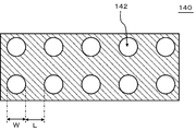
- FIG. 2 is a plan view of the second electrode 140.
- the plurality of openings 142 are formed in the second electrode 140.
- the width W of the opening 142 is preferably 150 ⁇ m or less from the viewpoint that it is not larger than a size that can be visually recognized by humans.
- the function of the optical element 102 decreases in the portion of the optical element 102 that overlaps the opening 142. .
- the optical element 102 is a light emitting element
- the width of the opening 142 is set to 150 ⁇ m or less, it becomes difficult for a person to visually recognize that the emission intensity is reduced in the portion of the optical element 102 overlapping the opening 142.
- the optical element 102 is a photoelectric conversion element, the charges generated in the organic layer 130 located in a portion overlapping with the opening 142 are easily collected by the second electrode 140 located in the periphery thereof.
- the interval L between the adjacent openings 142 is preferably 150 ⁇ m or less.
- the second electrode 140 is partially oxidized to partially increase the resistance. And when the 2nd electrode 140 becomes high resistance partially, the brightness
- the distance L between the adjacent second electrodes 140 is set to 150 ⁇ m or less, it is possible to suppress the width of the high-resistance portion of the second electrode 140 described above from exceeding 150 ⁇ m.
- the presence of the other opening 142 in a region having a distance of 150 ⁇ m or less from the predetermined opening 142 can suppress the width of the high resistance portion of the second electrode 140 from becoming larger than 150 ⁇ m. Therefore, even if the luminance of the optical element 102 is partially reduced, it is difficult for a person to visually recognize the reduced portion.
- the shape of the opening 142 is circular.
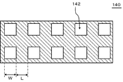
- the shape of the opening 142 is not limited to a circle.
- the shape of the opening 142 may be a polygon (for example, a rectangle) or an ellipse.
- at least one opening 142 may have a different shape from the other openings 142.
- the optical element 102 is formed on the substrate 110.
- the optical element 102 is sealed with a sealing member 180.
- an opening 142 is formed in the second electrode 140.
- positioning the desiccant 170 is also provided. Details will be described below.
- the substrate 110 is prepared.
- the substrate 110 may be formed in a sheet shape in advance, or may be formed in a sheet shape by a known technique such as spin coating by applying a resin on a support substrate different from the substrate 110.
- an inorganic layer 160 is formed on one surface of the substrate 110.
- the inorganic layer 160 is formed using, for example, a vapor deposition method, a sputtering method, a CVD method, or an ALD method. Note that a portion having a thin film or a pinhole may be formed in the inorganic layer 160 in some cases. When these are formed, moisture or the like passes through the substrate 110 from this portion.
- the first electrode 120 and the organic layer 130 are formed on the substrate 110.
- the first electrode 120 is formed by a dry method such as a coating method (wet method) such as an inkjet method, a sputtering method, or a vapor deposition method.
- the organic layer 130 is formed by, for example, a coating method or a vapor deposition method. Some layers of the organic layer 130 may be formed by a method different from other layers.
- the second electrode 140 is formed.
- the second electrode 140 is formed using, for example, a vapor deposition method.
- the opening 142 is formed by using, for example, a mask.
- a sealing member 180 is prepared. Then, a desiccant 170 is provided on the surface of the sealing member 180 that faces the optical element 102. Next, the desiccant 170 and the sealing member 180 are fixed on the second electrode 140 using the resin layer 150.
- an opening 142 is formed in the second electrode 140. For this reason, even if moisture or the like permeates the substrate 110, at least a part of the moisture is absorbed by the desiccant 170 through the opening 142 and the resin layer 150. Therefore, even when a substrate made of a resin is used as the substrate 110, it is possible to suppress deterioration of the optical element 102 due to accumulation of moisture or the like in the layer of the optical element 102 closer to the substrate 110 than the second electrode 140.
- the optical device 100 according to the present example is the same as the optical device 100 shown in the embodiment except for the manufacturing method of the second electrode 140.
- the second electrode 140 is formed by performing film formation by a vapor deposition method using a mask a plurality of times (for example, twice). At this time, the opening pattern of the mask is different for each film formation by the vapor deposition method.
- FIG. 4A is a plan view of the first mask 200 used in the first film formation
- FIG. 4B is a plan view of the second mask 202 used in the second film formation. It is.
- FIG. 4C is a plan view of the second electrode 140.
- each of the first mask 200 and the second mask 202 has a linear or dotted opening pattern, but these opening patterns extend. Directions are different from each other (for example, a crossing direction or a perpendicular direction).
- the portion of the second electrode 140 that becomes the optical element 102 includes a plurality of linear or dotted first conductive layers and a plurality of linear or dotted first conductive layers. The two conductive layers are formed so as to intersect with each other. The plurality of first conductive layers extend in parallel with each other, and the plurality of second conductive layers extend in parallel with each other.
- the second electrode 140 has an electrode extraction portion 141 formed therein.
- the electrode extraction portion 141 is formed in a portion of the second electrode that does not become the optical element 102 (that is, a portion that does not overlap with the organic layer 130), and the second electrode 140 is a conductive layer formed on the substrate 110. (For example, a wiring or a terminal).
- the electrode extraction part 141 does not have an opening in order to reduce the resistance.
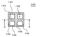
- FIG. 5 is a diagram schematically showing an enlarged portion of the second electrode 140 shown in FIG. 4C that overlaps the optical element 102.
- 6 is a cross-sectional view taken along the line AA in FIG.
- the second electrode 140 is formed by performing vacuum deposition a plurality of times (for example, twice). In each vacuum deposition, conductive layers (first conductive layer 144 and second conductive layer 146) extending in different directions are formed. As shown in FIG. 6, the second electrode 140 is thicker than the other part (thick film part) at the part where the first conductive layer 144 and the second conductive layer 146 intersect. Note that, in the portion where the first conductive layer 144 and the second conductive layer 146 overlap, the boundary between the first conductive layer 144 and the second conductive layer 146 may be clear or unclear.
- the second electrode 140 since the second electrode 140 has the opening 142, even if a substrate made of resin is used as the substrate 110, the layer on the substrate 110 side of the second electrode 140 in the optical element 102. It is possible to suppress the deterioration of the optical element 102 due to the accumulation of moisture or the like.
- the second electrode 140 is formed using a plurality of masks, a fine opening 142 can be easily formed. Further, by forming a plurality of linear openings from one end to the other end of the mask, the rigidity of the mask can be secured and a plurality of relatively small openings can be formed.
- FIG. 7 is a cross-sectional view illustrating the configuration of the optical device 100 according to the second embodiment.
- the optical device 100 according to the present example has the same configuration as that of the optical device 100 according to the embodiment or Example 1 except that the optical device 100 includes the inorganic layers 162 and 164 and the planarization layer 190.
- an inorganic layer 162 is formed on one surface of the substrate 110.
- the inorganic layer 162 is provided on the surface of the substrate 110 opposite to the inorganic layer 160.
- the inorganic layer 162 includes at least one layer of a silicon oxide film, a silicon nitride film, and a silicon oxynitride film, and is formed using a sputtering method, a CVD method, or an ALD method.
- a planarization layer 190 and an inorganic layer 164 are formed in this order.
- the planarization layer 190 planarizes the surface (first electrode 120 side) of the substrate 110, for example.
- the planarization layer 190 is provided to planarize the surface (first electrode 120 side) of the uneven inorganic layer 164 formed on one surface of the substrate 110, for example.
- the planarization layer 190 is formed by slit coating a resin such as epoxy or acrylic.
- the inorganic layer 164 includes at least one layer of a silicon oxide film, a silicon nitride film, and a silicon oxynitride film, and is formed using a sputtering method, a CVD method, or an ALD method.
- the second electrode 140 since the second electrode 140 has the opening 142, even if a substrate made of resin is used as the substrate 110, moisture in the layer closer to the substrate 110 than the second electrode 140 in the optical element 102 is obtained. It is possible to suppress the deterioration of the optical element 102 due to accumulation of the like. In addition, since the planarization layer 190 is provided, the yield of the optical element 102 can be improved. Furthermore, since the inorganic layers 162 and 164 are provided, it is possible to prevent moisture and the like from entering the optical element 102.
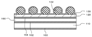
- FIG. 8 is a cross-sectional view illustrating the configuration of the optical device 100 according to the third embodiment.
- the optical device 100 according to the present example has the same configuration as the optical device 100 according to the embodiment or Example 2 except for the following points. This figure shows a case similar to the second embodiment.
- a plurality of particles 132 are positioned on the first electrode 120.
- the plurality of particles 132 are located in the opening 142.
- the diameter of the particle 132 is larger than the sum of the thicknesses of the organic layer 130, the second electrode 140, or the organic layer 130 and the second electrode 140, and is, for example, 100 nm or more and 100 ⁇ m or less.
- the particles 132 are arranged before the second electrode 140 is formed. Therefore, an opening 142 is formed in the second electrode 140 by the particles 132.
- the particles 132 are covered with a material constituting the organic layer 130.
- the material of the organic layer 130 covering the particles 132 may be a part of the layers constituting the organic layer 130.
- Particle 132 is an insulating inorganic material, but is preferably a hygroscopic material (eg, zeolite, silica gel). In this case, a desiccant is disposed in the opening 142. Note that the particles 132 may be formed of an oxide (eg, metal oxide) such as calcium oxide, magnesium oxide, zirconium oxide, yttrium oxide, aluminum oxide, or silicon oxide.
- oxide eg, metal oxide
- the 2nd electrode 140 when forming the 2nd electrode 140 by a vapor deposition method, the 2nd electrode 140 is also formed on the particle
- the second electrode 140 does not adhere to the lower half of the surface of the particle 132 (in other words, the surface facing the organic layer 130). For this reason, as shown in FIG. 9, the second electrode 140 has an opening 142 in a region overlapping the particle 132. Note that the central portion of the opening 142 is blocked by the particles 132.
- FIG. 10 is a diagram showing a first example of the arrangement method of the particles 132.
- the organic layer 130 for example, a hole transport layer
- grains 132 are contained in this coating liquid. For this reason, the particles 132 are disposed on the first electrode 120 when the organic layer 130 is formed by a coating method.
- FIG. 11 is a diagram showing a second example of the arrangement method of the particles 132.
- the particles 132 are disposed on the first electrode 120 before the organic layer 130 is formed.
- the particles 132 are arranged by applying a coating liquid containing the particles 132 to the first electrode 120.
- FIG. 12 is a diagram showing a third example of the arrangement method of the particles 132.
- the particles 132 are disposed on the organic layer 130 after forming the organic layer 130 and before forming the second electrode 140.
- the particles 132 are arranged by applying a coating solution containing the particles 132 to the organic layer 130.
- the second electrode 140 may be formed by a method similar to the method (embodiment 1) shown in FIGS.
- the substrate 110 Even in this embodiment, even when a substrate made of a resin is used as the substrate 110, it is possible to suppress deterioration of the optical element 102 due to accumulation of moisture or the like in the layer on the substrate 110 side of the second electrode 140 in the optical element 102. . In addition, when a hygroscopic material is used as the particles 132, moisture transmitted through the substrate 110 is also absorbed by the particles 132, so that deterioration of the optical element 102 can be further suppressed.
Landscapes
- Electroluminescent Light Sources (AREA)
- Photovoltaic Devices (AREA)
Abstract
Selon l'invention, un substrat est configuré à partir d'une résine. Un élément optique (102) comporte une première électrode (120), une couche organique (130) et une seconde électrode (140). La première électrode (120) est positionnée entre la couche organique (130) et le substrat (110). La seconde électrode (140) prend en sandwich la couche organique (130) entre la première électrode (120) et ladite seconde électrode. La seconde électrode (140) possède une ouverture (142). Un dispositif optique (100) possède également un élément desséchant (170). L'élément desséchant (170) est disposé dans l'ouverture (142) ou entre la seconde électrode (140) et un élément étanchéification (180). L'élément desséchant (170) est disposé, par exemple, entre la seconde électrode (140) et l'élément d'étanchéification (180).
Priority Applications (2)
| Application Number | Priority Date | Filing Date | Title |
|---|---|---|---|
| PCT/JP2013/085152 WO2015097877A1 (fr) | 2013-12-27 | 2013-12-27 | Dispositif optique et son procédé de fabrication |
| JP2015554456A JPWO2015097877A1 (ja) | 2013-12-27 | 2013-12-27 | 光装置及び光装置の製造方法 |
Applications Claiming Priority (1)
| Application Number | Priority Date | Filing Date | Title |
|---|---|---|---|
| PCT/JP2013/085152 WO2015097877A1 (fr) | 2013-12-27 | 2013-12-27 | Dispositif optique et son procédé de fabrication |
Publications (1)
| Publication Number | Publication Date |
|---|---|
| WO2015097877A1 true WO2015097877A1 (fr) | 2015-07-02 |
Family
ID=53477807
Family Applications (1)
| Application Number | Title | Priority Date | Filing Date |
|---|---|---|---|
| PCT/JP2013/085152 Ceased WO2015097877A1 (fr) | 2013-12-27 | 2013-12-27 | Dispositif optique et son procédé de fabrication |
Country Status (2)
| Country | Link |
|---|---|
| JP (1) | JPWO2015097877A1 (fr) |
| WO (1) | WO2015097877A1 (fr) |
Cited By (1)
| Publication number | Priority date | Publication date | Assignee | Title |
|---|---|---|---|---|
| JPWO2017065058A1 (ja) * | 2015-10-16 | 2018-08-02 | 住友化学株式会社 | 有機光電変換素子 |
Citations (7)
| Publication number | Priority date | Publication date | Assignee | Title |
|---|---|---|---|---|
| JP2003092191A (ja) * | 2001-07-11 | 2003-03-28 | Semiconductor Energy Lab Co Ltd | 発光装置及びその作製方法 |
| JP2008234921A (ja) * | 2007-03-19 | 2008-10-02 | Seiko Epson Corp | エレクトロルミネッセンス装置及び電子機器 |
| JP2009026648A (ja) * | 2007-07-20 | 2009-02-05 | Pioneer Electronic Corp | 有機elパネル及びその製造方法 |
| JP2009037810A (ja) * | 2007-07-31 | 2009-02-19 | Sumitomo Chemical Co Ltd | 有機エレクトロルミネッセンス素子およびその製造方法 |
| JP2011204645A (ja) * | 2010-03-26 | 2011-10-13 | Panasonic Electric Works Co Ltd | 発光装置 |
| JP2012028338A (ja) * | 2011-09-30 | 2012-02-09 | Sumitomo Chemical Co Ltd | 有機エレクトロルミネッセンス素子およびその製造方法 |
| JP2013157340A (ja) * | 2010-11-02 | 2013-08-15 | Oji Holdings Corp | 有機発光ダイオードおよびその製造方法、画像表示装置および照明装置 |
Family Cites Families (1)
| Publication number | Priority date | Publication date | Assignee | Title |
|---|---|---|---|---|
| US20070013293A1 (en) * | 2005-07-12 | 2007-01-18 | Eastman Kodak Company | OLED device having spacers |
-
2013
- 2013-12-27 WO PCT/JP2013/085152 patent/WO2015097877A1/fr not_active Ceased
- 2013-12-27 JP JP2015554456A patent/JPWO2015097877A1/ja active Pending
Patent Citations (7)
| Publication number | Priority date | Publication date | Assignee | Title |
|---|---|---|---|---|
| JP2003092191A (ja) * | 2001-07-11 | 2003-03-28 | Semiconductor Energy Lab Co Ltd | 発光装置及びその作製方法 |
| JP2008234921A (ja) * | 2007-03-19 | 2008-10-02 | Seiko Epson Corp | エレクトロルミネッセンス装置及び電子機器 |
| JP2009026648A (ja) * | 2007-07-20 | 2009-02-05 | Pioneer Electronic Corp | 有機elパネル及びその製造方法 |
| JP2009037810A (ja) * | 2007-07-31 | 2009-02-19 | Sumitomo Chemical Co Ltd | 有機エレクトロルミネッセンス素子およびその製造方法 |
| JP2011204645A (ja) * | 2010-03-26 | 2011-10-13 | Panasonic Electric Works Co Ltd | 発光装置 |
| JP2013157340A (ja) * | 2010-11-02 | 2013-08-15 | Oji Holdings Corp | 有機発光ダイオードおよびその製造方法、画像表示装置および照明装置 |
| JP2012028338A (ja) * | 2011-09-30 | 2012-02-09 | Sumitomo Chemical Co Ltd | 有機エレクトロルミネッセンス素子およびその製造方法 |
Cited By (3)
| Publication number | Priority date | Publication date | Assignee | Title |
|---|---|---|---|---|
| JPWO2017065058A1 (ja) * | 2015-10-16 | 2018-08-02 | 住友化学株式会社 | 有機光電変換素子 |
| EP3364473A4 (fr) * | 2015-10-16 | 2019-06-12 | Sumitomo Chemical Company, Limited | Élément de conversion photoélectrique organique |
| JP7166756B2 (ja) | 2015-10-16 | 2022-11-08 | 住友化学株式会社 | 有機光電変換素子 |
Also Published As
| Publication number | Publication date |
|---|---|
| JPWO2015097877A1 (ja) | 2017-03-23 |
Similar Documents
| Publication | Publication Date | Title |
|---|---|---|
| CN113141779B (zh) | 显示基板及其制作方法和显示装置 | |
| TWI556485B (zh) | 光電裝置封裝結構及光電裝置陣列 | |
| KR101642656B1 (ko) | 유기 반도체 소자 및 유기 반도체 소자의 제조 방법 | |
| TWI524515B (zh) | 光電裝置陣列 | |
| JP2013506958A (ja) | モノリシック並列相互接続構造 | |
| JP6463354B2 (ja) | 発光装置 | |
| WO2015097877A1 (fr) | Dispositif optique et son procédé de fabrication | |
| JP2007179914A (ja) | El装置及びその製造方法 | |
| JP2018077499A (ja) | 光学装置 | |
| JP2007179913A (ja) | El装置及びその製造方法 | |
| KR20160055142A (ko) | 복사선 방출 장치 및 그 제조 방법 | |
| JP2015220091A (ja) | 発光装置 | |
| JP2019133959A (ja) | 発光装置 | |
| JP2014203526A (ja) | 接合構造および発光装置 | |
| US20170256592A1 (en) | Radiation-emitting apparatus and method for producing same | |
| WO2014162446A1 (fr) | Structure de jonction et dispositif électroluminescent | |
| WO2016046914A1 (fr) | Dispositif électroluminescent | |
| JP2018156722A (ja) | 有機elパネル | |
| JP2019050433A (ja) | 発光装置 | |
| JP2017162765A (ja) | 発光装置 | |
| WO2017154207A1 (fr) | Dispositif électroluminescent | |
| JP2014203527A (ja) | 接合構造および発光装置 | |
| JP2016134329A (ja) | 発光装置 | |
| JP2016085923A (ja) | 発光装置 | |
| JP2016100314A (ja) | 発光装置 |
Legal Events
| Date | Code | Title | Description |
|---|---|---|---|
| 121 | Ep: the epo has been informed by wipo that ep was designated in this application |
Ref document number: 13900117 Country of ref document: EP Kind code of ref document: A1 |
|
| ENP | Entry into the national phase |
Ref document number: 2015554456 Country of ref document: JP Kind code of ref document: A |
|
| NENP | Non-entry into the national phase |
Ref country code: DE |
|
| 122 | Ep: pct application non-entry in european phase |
Ref document number: 13900117 Country of ref document: EP Kind code of ref document: A1 |