WO2015098609A1 - ハンドル基板、半導体用複合基板、半導体回路基板およびその製造方法 - Google Patents
ハンドル基板、半導体用複合基板、半導体回路基板およびその製造方法 Download PDFInfo
- Publication number
- WO2015098609A1 WO2015098609A1 PCT/JP2014/083209 JP2014083209W WO2015098609A1 WO 2015098609 A1 WO2015098609 A1 WO 2015098609A1 JP 2014083209 W JP2014083209 W JP 2014083209W WO 2015098609 A1 WO2015098609 A1 WO 2015098609A1
- Authority
- WO
- WIPO (PCT)
- Prior art keywords
- substrate
- handle
- semiconductor
- alumina
- donor
- Prior art date
- Legal status (The legal status is an assumption and is not a legal conclusion. Google has not performed a legal analysis and makes no representation as to the accuracy of the status listed.)
- Ceased
Links
Images


Classifications
-
- H—ELECTRICITY
- H10—SEMICONDUCTOR DEVICES; ELECTRIC SOLID-STATE DEVICES NOT OTHERWISE PROVIDED FOR
- H10P—GENERIC PROCESSES OR APPARATUS FOR THE MANUFACTURE OR TREATMENT OF DEVICES COVERED BY CLASS H10
- H10P90/00—Preparation of wafers not covered by a single main group of this subclass, e.g. wafer reinforcement
- H10P90/19—Preparing inhomogeneous wafers
- H10P90/1904—Preparing vertically inhomogeneous wafers
- H10P90/1906—Preparing SOI wafers
- H10P90/1914—Preparing SOI wafers using bonding
- H10P90/1916—Preparing SOI wafers using bonding with separation or delamination along an ion implanted layer, e.g. Smart-cut
-
- C—CHEMISTRY; METALLURGY
- C01—INORGANIC CHEMISTRY
- C01F—COMPOUNDS OF THE METALS BERYLLIUM, MAGNESIUM, ALUMINIUM, CALCIUM, STRONTIUM, BARIUM, RADIUM, THORIUM, OR OF THE RARE-EARTH METALS
- C01F7/00—Compounds of aluminium
- C01F7/02—Aluminium oxide; Aluminium hydroxide; Aluminates
-
- C—CHEMISTRY; METALLURGY
- C04—CEMENTS; CONCRETE; ARTIFICIAL STONE; CERAMICS; REFRACTORIES
- C04B—LIME, MAGNESIA; SLAG; CEMENTS; COMPOSITIONS THEREOF, e.g. MORTARS, CONCRETE OR LIKE BUILDING MATERIALS; ARTIFICIAL STONE; CERAMICS; REFRACTORIES; TREATMENT OF NATURAL STONE
- C04B35/00—Shaped ceramic products characterised by their composition; Ceramics compositions; Processing powders of inorganic compounds preparatory to the manufacturing of ceramic products
- C04B35/01—Shaped ceramic products characterised by their composition; Ceramics compositions; Processing powders of inorganic compounds preparatory to the manufacturing of ceramic products based on oxide ceramics
- C04B35/10—Shaped ceramic products characterised by their composition; Ceramics compositions; Processing powders of inorganic compounds preparatory to the manufacturing of ceramic products based on oxide ceramics based on aluminium oxide
-
- C—CHEMISTRY; METALLURGY
- C04—CEMENTS; CONCRETE; ARTIFICIAL STONE; CERAMICS; REFRACTORIES
- C04B—LIME, MAGNESIA; SLAG; CEMENTS; COMPOSITIONS THEREOF, e.g. MORTARS, CONCRETE OR LIKE BUILDING MATERIALS; ARTIFICIAL STONE; CERAMICS; REFRACTORIES; TREATMENT OF NATURAL STONE
- C04B35/00—Shaped ceramic products characterised by their composition; Ceramics compositions; Processing powders of inorganic compounds preparatory to the manufacturing of ceramic products
- C04B35/01—Shaped ceramic products characterised by their composition; Ceramics compositions; Processing powders of inorganic compounds preparatory to the manufacturing of ceramic products based on oxide ceramics
- C04B35/10—Shaped ceramic products characterised by their composition; Ceramics compositions; Processing powders of inorganic compounds preparatory to the manufacturing of ceramic products based on oxide ceramics based on aluminium oxide
- C04B35/111—Fine ceramics
- C04B35/115—Translucent or transparent products
-
- C—CHEMISTRY; METALLURGY
- C04—CEMENTS; CONCRETE; ARTIFICIAL STONE; CERAMICS; REFRACTORIES
- C04B—LIME, MAGNESIA; SLAG; CEMENTS; COMPOSITIONS THEREOF, e.g. MORTARS, CONCRETE OR LIKE BUILDING MATERIALS; ARTIFICIAL STONE; CERAMICS; REFRACTORIES; TREATMENT OF NATURAL STONE
- C04B35/00—Shaped ceramic products characterised by their composition; Ceramics compositions; Processing powders of inorganic compounds preparatory to the manufacturing of ceramic products
- C04B35/622—Forming processes; Processing powders of inorganic compounds preparatory to the manufacturing of ceramic products
- C04B35/64—Burning or sintering processes
-
- C—CHEMISTRY; METALLURGY
- C04—CEMENTS; CONCRETE; ARTIFICIAL STONE; CERAMICS; REFRACTORIES
- C04B—LIME, MAGNESIA; SLAG; CEMENTS; COMPOSITIONS THEREOF, e.g. MORTARS, CONCRETE OR LIKE BUILDING MATERIALS; ARTIFICIAL STONE; CERAMICS; REFRACTORIES; TREATMENT OF NATURAL STONE
- C04B37/00—Joining burned ceramic articles with other burned ceramic articles or other articles by heating
- C04B37/001—Joining burned ceramic articles with other burned ceramic articles or other articles by heating directly with other burned ceramic articles
-
- H—ELECTRICITY
- H10—SEMICONDUCTOR DEVICES; ELECTRIC SOLID-STATE DEVICES NOT OTHERWISE PROVIDED FOR
- H10D—INORGANIC ELECTRIC SEMICONDUCTOR DEVICES
- H10D62/00—Semiconductor bodies, or regions thereof, of devices having potential barriers
- H10D62/10—Shapes, relative sizes or dispositions of the regions of the semiconductor bodies; Shapes of the semiconductor bodies
-
- H—ELECTRICITY
- H10—SEMICONDUCTOR DEVICES; ELECTRIC SOLID-STATE DEVICES NOT OTHERWISE PROVIDED FOR
- H10D—INORGANIC ELECTRIC SEMICONDUCTOR DEVICES
- H10D86/00—Integrated devices formed in or on insulating or conducting substrates, e.g. formed in silicon-on-insulator [SOI] substrates or on stainless steel or glass substrates
-
- H—ELECTRICITY
- H10—SEMICONDUCTOR DEVICES; ELECTRIC SOLID-STATE DEVICES NOT OTHERWISE PROVIDED FOR
- H10P—GENERIC PROCESSES OR APPARATUS FOR THE MANUFACTURE OR TREATMENT OF DEVICES COVERED BY CLASS H10
- H10P72/00—Handling or holding of wafers, substrates or devices during manufacture or treatment thereof
- H10P72/70—Handling or holding of wafers, substrates or devices during manufacture or treatment thereof for supporting or gripping
- H10P72/74—Handling or holding of wafers, substrates or devices during manufacture or treatment thereof for supporting or gripping using temporarily an auxiliary support
-
- H—ELECTRICITY
- H10—SEMICONDUCTOR DEVICES; ELECTRIC SOLID-STATE DEVICES NOT OTHERWISE PROVIDED FOR
- H10P—GENERIC PROCESSES OR APPARATUS FOR THE MANUFACTURE OR TREATMENT OF DEVICES COVERED BY CLASS H10
- H10P90/00—Preparation of wafers not covered by a single main group of this subclass, e.g. wafer reinforcement
-
- H—ELECTRICITY
- H10—SEMICONDUCTOR DEVICES; ELECTRIC SOLID-STATE DEVICES NOT OTHERWISE PROVIDED FOR
- H10W—GENERIC PACKAGES, INTERCONNECTIONS, CONNECTORS OR OTHER CONSTRUCTIONAL DETAILS OF DEVICES COVERED BY CLASS H10
- H10W10/00—Isolation regions in semiconductor bodies between components of integrated devices
- H10W10/10—Isolation regions comprising dielectric materials
- H10W10/181—Semiconductor-on-insulator [SOI] isolation regions, e.g. buried oxide regions of SOI wafers
-
- H—ELECTRICITY
- H10—SEMICONDUCTOR DEVICES; ELECTRIC SOLID-STATE DEVICES NOT OTHERWISE PROVIDED FOR
- H10W—GENERIC PACKAGES, INTERCONNECTIONS, CONNECTORS OR OTHER CONSTRUCTIONAL DETAILS OF DEVICES COVERED BY CLASS H10
- H10W70/00—Package substrates; Interposers; Redistribution layers [RDL]
- H10W70/60—Insulating or insulated package substrates; Interposers; Redistribution layers
- H10W70/67—Insulating or insulated package substrates; Interposers; Redistribution layers characterised by their insulating layers or insulating parts
- H10W70/69—Insulating materials thereof
- H10W70/692—Ceramics or glasses
-
- C—CHEMISTRY; METALLURGY
- C01—INORGANIC CHEMISTRY
- C01P—INDEXING SCHEME RELATING TO STRUCTURAL AND PHYSICAL ASPECTS OF SOLID INORGANIC COMPOUNDS
- C01P2006/00—Physical properties of inorganic compounds
- C01P2006/60—Optical properties, e.g. expressed in CIELAB-values
-
- C—CHEMISTRY; METALLURGY
- C04—CEMENTS; CONCRETE; ARTIFICIAL STONE; CERAMICS; REFRACTORIES
- C04B—LIME, MAGNESIA; SLAG; CEMENTS; COMPOSITIONS THEREOF, e.g. MORTARS, CONCRETE OR LIKE BUILDING MATERIALS; ARTIFICIAL STONE; CERAMICS; REFRACTORIES; TREATMENT OF NATURAL STONE
- C04B2235/00—Aspects relating to ceramic starting mixtures or sintered ceramic products
- C04B2235/02—Composition of constituents of the starting material or of secondary phases of the final product
- C04B2235/30—Constituents and secondary phases not being of a fibrous nature
- C04B2235/32—Metal oxides, mixed metal oxides, or oxide-forming salts thereof, e.g. carbonates, nitrates, (oxy)hydroxides, chlorides
- C04B2235/3205—Alkaline earth oxides or oxide forming salts thereof, e.g. beryllium oxide
- C04B2235/3206—Magnesium oxides or oxide-forming salts thereof
-
- C—CHEMISTRY; METALLURGY
- C04—CEMENTS; CONCRETE; ARTIFICIAL STONE; CERAMICS; REFRACTORIES
- C04B—LIME, MAGNESIA; SLAG; CEMENTS; COMPOSITIONS THEREOF, e.g. MORTARS, CONCRETE OR LIKE BUILDING MATERIALS; ARTIFICIAL STONE; CERAMICS; REFRACTORIES; TREATMENT OF NATURAL STONE
- C04B2235/00—Aspects relating to ceramic starting mixtures or sintered ceramic products
- C04B2235/02—Composition of constituents of the starting material or of secondary phases of the final product
- C04B2235/30—Constituents and secondary phases not being of a fibrous nature
- C04B2235/32—Metal oxides, mixed metal oxides, or oxide-forming salts thereof, e.g. carbonates, nitrates, (oxy)hydroxides, chlorides
- C04B2235/3224—Rare earth oxide or oxide forming salts thereof, e.g. scandium oxide
- C04B2235/3225—Yttrium oxide or oxide-forming salts thereof
-
- C—CHEMISTRY; METALLURGY
- C04—CEMENTS; CONCRETE; ARTIFICIAL STONE; CERAMICS; REFRACTORIES
- C04B—LIME, MAGNESIA; SLAG; CEMENTS; COMPOSITIONS THEREOF, e.g. MORTARS, CONCRETE OR LIKE BUILDING MATERIALS; ARTIFICIAL STONE; CERAMICS; REFRACTORIES; TREATMENT OF NATURAL STONE
- C04B2235/00—Aspects relating to ceramic starting mixtures or sintered ceramic products
- C04B2235/02—Composition of constituents of the starting material or of secondary phases of the final product
- C04B2235/30—Constituents and secondary phases not being of a fibrous nature
- C04B2235/32—Metal oxides, mixed metal oxides, or oxide-forming salts thereof, e.g. carbonates, nitrates, (oxy)hydroxides, chlorides
- C04B2235/3231—Refractory metal oxides, their mixed metal oxides, or oxide-forming salts thereof
- C04B2235/3244—Zirconium oxides, zirconates, hafnium oxides, hafnates, or oxide-forming salts thereof
-
- C—CHEMISTRY; METALLURGY
- C04—CEMENTS; CONCRETE; ARTIFICIAL STONE; CERAMICS; REFRACTORIES
- C04B—LIME, MAGNESIA; SLAG; CEMENTS; COMPOSITIONS THEREOF, e.g. MORTARS, CONCRETE OR LIKE BUILDING MATERIALS; ARTIFICIAL STONE; CERAMICS; REFRACTORIES; TREATMENT OF NATURAL STONE
- C04B2235/00—Aspects relating to ceramic starting mixtures or sintered ceramic products
- C04B2235/02—Composition of constituents of the starting material or of secondary phases of the final product
- C04B2235/50—Constituents or additives of the starting mixture chosen for their shape or used because of their shape or their physical appearance
- C04B2235/54—Particle size related information
- C04B2235/5409—Particle size related information expressed by specific surface values
-
- C—CHEMISTRY; METALLURGY
- C04—CEMENTS; CONCRETE; ARTIFICIAL STONE; CERAMICS; REFRACTORIES
- C04B—LIME, MAGNESIA; SLAG; CEMENTS; COMPOSITIONS THEREOF, e.g. MORTARS, CONCRETE OR LIKE BUILDING MATERIALS; ARTIFICIAL STONE; CERAMICS; REFRACTORIES; TREATMENT OF NATURAL STONE
- C04B2235/00—Aspects relating to ceramic starting mixtures or sintered ceramic products
- C04B2235/02—Composition of constituents of the starting material or of secondary phases of the final product
- C04B2235/50—Constituents or additives of the starting mixture chosen for their shape or used because of their shape or their physical appearance
- C04B2235/54—Particle size related information
- C04B2235/5418—Particle size related information expressed by the size of the particles or aggregates thereof
- C04B2235/5445—Particle size related information expressed by the size of the particles or aggregates thereof submicron sized, i.e. from 0,1 to 1 micron
-
- C—CHEMISTRY; METALLURGY
- C04—CEMENTS; CONCRETE; ARTIFICIAL STONE; CERAMICS; REFRACTORIES
- C04B—LIME, MAGNESIA; SLAG; CEMENTS; COMPOSITIONS THEREOF, e.g. MORTARS, CONCRETE OR LIKE BUILDING MATERIALS; ARTIFICIAL STONE; CERAMICS; REFRACTORIES; TREATMENT OF NATURAL STONE
- C04B2235/00—Aspects relating to ceramic starting mixtures or sintered ceramic products
- C04B2235/60—Aspects relating to the preparation, properties or mechanical treatment of green bodies or pre-forms
- C04B2235/602—Making the green bodies or pre-forms by moulding
- C04B2235/6025—Tape casting, e.g. with a doctor blade
-
- C—CHEMISTRY; METALLURGY
- C04—CEMENTS; CONCRETE; ARTIFICIAL STONE; CERAMICS; REFRACTORIES
- C04B—LIME, MAGNESIA; SLAG; CEMENTS; COMPOSITIONS THEREOF, e.g. MORTARS, CONCRETE OR LIKE BUILDING MATERIALS; ARTIFICIAL STONE; CERAMICS; REFRACTORIES; TREATMENT OF NATURAL STONE
- C04B2235/00—Aspects relating to ceramic starting mixtures or sintered ceramic products
- C04B2235/65—Aspects relating to heat treatments of ceramic bodies such as green ceramics or pre-sintered ceramics, e.g. burning, sintering or melting processes
- C04B2235/656—Aspects relating to heat treatments of ceramic bodies such as green ceramics or pre-sintered ceramics, e.g. burning, sintering or melting processes characterised by specific heating conditions during heat treatment
- C04B2235/6562—Heating rate
-
- C—CHEMISTRY; METALLURGY
- C04—CEMENTS; CONCRETE; ARTIFICIAL STONE; CERAMICS; REFRACTORIES
- C04B—LIME, MAGNESIA; SLAG; CEMENTS; COMPOSITIONS THEREOF, e.g. MORTARS, CONCRETE OR LIKE BUILDING MATERIALS; ARTIFICIAL STONE; CERAMICS; REFRACTORIES; TREATMENT OF NATURAL STONE
- C04B2235/00—Aspects relating to ceramic starting mixtures or sintered ceramic products
- C04B2235/65—Aspects relating to heat treatments of ceramic bodies such as green ceramics or pre-sintered ceramics, e.g. burning, sintering or melting processes
- C04B2235/658—Atmosphere during thermal treatment
- C04B2235/6582—Hydrogen containing atmosphere
-
- C—CHEMISTRY; METALLURGY
- C04—CEMENTS; CONCRETE; ARTIFICIAL STONE; CERAMICS; REFRACTORIES
- C04B—LIME, MAGNESIA; SLAG; CEMENTS; COMPOSITIONS THEREOF, e.g. MORTARS, CONCRETE OR LIKE BUILDING MATERIALS; ARTIFICIAL STONE; CERAMICS; REFRACTORIES; TREATMENT OF NATURAL STONE
- C04B2235/00—Aspects relating to ceramic starting mixtures or sintered ceramic products
- C04B2235/65—Aspects relating to heat treatments of ceramic bodies such as green ceramics or pre-sintered ceramics, e.g. burning, sintering or melting processes
- C04B2235/66—Specific sintering techniques, e.g. centrifugal sintering
- C04B2235/661—Multi-step sintering
-
- C—CHEMISTRY; METALLURGY
- C04—CEMENTS; CONCRETE; ARTIFICIAL STONE; CERAMICS; REFRACTORIES
- C04B—LIME, MAGNESIA; SLAG; CEMENTS; COMPOSITIONS THEREOF, e.g. MORTARS, CONCRETE OR LIKE BUILDING MATERIALS; ARTIFICIAL STONE; CERAMICS; REFRACTORIES; TREATMENT OF NATURAL STONE
- C04B2235/00—Aspects relating to ceramic starting mixtures or sintered ceramic products
- C04B2235/65—Aspects relating to heat treatments of ceramic bodies such as green ceramics or pre-sintered ceramics, e.g. burning, sintering or melting processes
- C04B2235/66—Specific sintering techniques, e.g. centrifugal sintering
- C04B2235/661—Multi-step sintering
- C04B2235/662—Annealing after sintering
-
- C—CHEMISTRY; METALLURGY
- C04—CEMENTS; CONCRETE; ARTIFICIAL STONE; CERAMICS; REFRACTORIES
- C04B—LIME, MAGNESIA; SLAG; CEMENTS; COMPOSITIONS THEREOF, e.g. MORTARS, CONCRETE OR LIKE BUILDING MATERIALS; ARTIFICIAL STONE; CERAMICS; REFRACTORIES; TREATMENT OF NATURAL STONE
- C04B2235/00—Aspects relating to ceramic starting mixtures or sintered ceramic products
- C04B2235/70—Aspects relating to sintered or melt-casted ceramic products
- C04B2235/74—Physical characteristics
- C04B2235/78—Grain sizes and shapes, product microstructures, e.g. acicular grains, equiaxed grains, platelet-structures
- C04B2235/786—Micrometer sized grains, i.e. from 1 to 100 micron
-
- C—CHEMISTRY; METALLURGY
- C04—CEMENTS; CONCRETE; ARTIFICIAL STONE; CERAMICS; REFRACTORIES
- C04B—LIME, MAGNESIA; SLAG; CEMENTS; COMPOSITIONS THEREOF, e.g. MORTARS, CONCRETE OR LIKE BUILDING MATERIALS; ARTIFICIAL STONE; CERAMICS; REFRACTORIES; TREATMENT OF NATURAL STONE
- C04B2237/00—Aspects relating to ceramic laminates or to joining of ceramic articles with other articles by heating
- C04B2237/30—Composition of layers of ceramic laminates or of ceramic or metallic articles to be joined by heating, e.g. Si substrates
- C04B2237/32—Ceramic
- C04B2237/34—Oxidic
- C04B2237/343—Alumina or aluminates
-
- C—CHEMISTRY; METALLURGY
- C04—CEMENTS; CONCRETE; ARTIFICIAL STONE; CERAMICS; REFRACTORIES
- C04B—LIME, MAGNESIA; SLAG; CEMENTS; COMPOSITIONS THEREOF, e.g. MORTARS, CONCRETE OR LIKE BUILDING MATERIALS; ARTIFICIAL STONE; CERAMICS; REFRACTORIES; TREATMENT OF NATURAL STONE
- C04B2237/00—Aspects relating to ceramic laminates or to joining of ceramic articles with other articles by heating
- C04B2237/50—Processing aspects relating to ceramic laminates or to the joining of ceramic articles with other articles by heating
- C04B2237/70—Forming laminates or joined articles comprising layers of a specific, unusual thickness
-
- C—CHEMISTRY; METALLURGY
- C04—CEMENTS; CONCRETE; ARTIFICIAL STONE; CERAMICS; REFRACTORIES
- C04B—LIME, MAGNESIA; SLAG; CEMENTS; COMPOSITIONS THEREOF, e.g. MORTARS, CONCRETE OR LIKE BUILDING MATERIALS; ARTIFICIAL STONE; CERAMICS; REFRACTORIES; TREATMENT OF NATURAL STONE
- C04B2237/00—Aspects relating to ceramic laminates or to joining of ceramic articles with other articles by heating
- C04B2237/50—Processing aspects relating to ceramic laminates or to the joining of ceramic articles with other articles by heating
- C04B2237/70—Forming laminates or joined articles comprising layers of a specific, unusual thickness
- C04B2237/704—Forming laminates or joined articles comprising layers of a specific, unusual thickness of one or more of the ceramic layers or articles
-
- H—ELECTRICITY
- H10—SEMICONDUCTOR DEVICES; ELECTRIC SOLID-STATE DEVICES NOT OTHERWISE PROVIDED FOR
- H10D—INORGANIC ELECTRIC SEMICONDUCTOR DEVICES
- H10D86/00—Integrated devices formed in or on insulating or conducting substrates, e.g. formed in silicon-on-insulator [SOI] substrates or on stainless steel or glass substrates
- H10D86/01—Manufacture or treatment
- H10D86/021—Manufacture or treatment of multiple TFTs
- H10D86/0214—Manufacture or treatment of multiple TFTs using temporary substrates
-
- H—ELECTRICITY
- H10—SEMICONDUCTOR DEVICES; ELECTRIC SOLID-STATE DEVICES NOT OTHERWISE PROVIDED FOR
- H10P—GENERIC PROCESSES OR APPARATUS FOR THE MANUFACTURE OR TREATMENT OF DEVICES COVERED BY CLASS H10
- H10P72/00—Handling or holding of wafers, substrates or devices during manufacture or treatment thereof
- H10P72/70—Handling or holding of wafers, substrates or devices during manufacture or treatment thereof for supporting or gripping
- H10P72/74—Handling or holding of wafers, substrates or devices during manufacture or treatment thereof for supporting or gripping using temporarily an auxiliary support
- H10P72/7416—Handling or holding of wafers, substrates or devices during manufacture or treatment thereof for supporting or gripping using temporarily an auxiliary support used during dicing or grinding
-
- H—ELECTRICITY
- H10—SEMICONDUCTOR DEVICES; ELECTRIC SOLID-STATE DEVICES NOT OTHERWISE PROVIDED FOR
- H10P—GENERIC PROCESSES OR APPARATUS FOR THE MANUFACTURE OR TREATMENT OF DEVICES COVERED BY CLASS H10
- H10P72/00—Handling or holding of wafers, substrates or devices during manufacture or treatment thereof
- H10P72/70—Handling or holding of wafers, substrates or devices during manufacture or treatment thereof for supporting or gripping
- H10P72/74—Handling or holding of wafers, substrates or devices during manufacture or treatment thereof for supporting or gripping using temporarily an auxiliary support
- H10P72/7438—Handling or holding of wafers, substrates or devices during manufacture or treatment thereof for supporting or gripping using temporarily an auxiliary support with parts of the auxiliary support remaining in the finished device
-
- H—ELECTRICITY
- H10—SEMICONDUCTOR DEVICES; ELECTRIC SOLID-STATE DEVICES NOT OTHERWISE PROVIDED FOR
- H10P—GENERIC PROCESSES OR APPARATUS FOR THE MANUFACTURE OR TREATMENT OF DEVICES COVERED BY CLASS H10
- H10P72/00—Handling or holding of wafers, substrates or devices during manufacture or treatment thereof
- H10P72/70—Handling or holding of wafers, substrates or devices during manufacture or treatment thereof for supporting or gripping
- H10P72/74—Handling or holding of wafers, substrates or devices during manufacture or treatment thereof for supporting or gripping using temporarily an auxiliary support
- H10P72/744—Details of chemical or physical process used for separating the auxiliary support from a device or a wafer
Definitions
- the present invention relates to a handle substrate, a semiconductor composite substrate, a semiconductor circuit substrate, and a manufacturing method thereof.
- SOQ Silicon Quartz
- SOG Silicon Glass
- SOS Silicon Sapphire SO
- a transparent wide gap such as SOI, GaN, ZnO, diamond, AlN, etc. in which the handle substrate is made of a transparent / insulating substrate.
- a bonded wafer obtained by bonding a semiconductor to a donor substrate such as silicon is known.
- SOQ, SOG, SOS, and the like are expected to be applied to projectors, high-frequency devices, and the like because of the insulation and transparency of the handle substrate.
- bonded wafers in which a wide gap semiconductor thin film is combined with a handle substrate are expected to be applied to high performance lasers and power devices.
- Such a composite substrate for a semiconductor includes a handle substrate and a donor substrate.
- the handle substrate and the donor substrate are made of a single crystal material.
- a method of forming a silicon layer on a base substrate by epitaxial growth has been the mainstream.
- a method of forming a silicon layer by direct bonding has been developed, which contributes to improving the performance of semiconductor devices. (Patent Documents 1, 2, and 3). That is, the handle substrate and the donor substrate are bonded via a bonding layer or an adhesive layer, or directly bonded.
- Such a semiconductor device is required to have a low profile as the equipment to be mounted is highly functional and downsized.
- the main surface on the side where the semiconductor device of the composite substrate formed by bonding ( The main surface (opposite surface) opposite to the main surface on the circuit side is processed by grinding, polishing, etching, or the like to reduce the thickness.
- the thickness of the composite substrate is reduced, the substrate is likely to be warped, which hinders handling. For this reason, a method is known in which handling is possible by bonding a separate support substrate to the main surface of the composite substrate on the circuit side (Patent Document 8).
- the ultraviolet curable resin When irradiating the ultraviolet curable resin with the ultraviolet curable resin interposed between the composite substrate and the separate support substrate, the ultraviolet curable resin may be irradiated from the side of the supporting substrate, It should be possible to irradiate from the composite substrate side.
- the material of the support substrate when ultraviolet light is irradiated from the support substrate side, the material of the support substrate must be a material that transmits ultraviolet light. Depending on the backside processing process after bonding, the support substrate must have properties such as mechanical strength, chemical resistance, and thermal expansion matching with the substrate to be bonded. Since the selection range of the material is narrowed, it is not preferable from the viewpoint of productivity. From this viewpoint, it can be said that it is preferable to irradiate ultraviolet rays from the composite substrate side.
- the support substrate is bonded to the composite substrate with an ultraviolet curable resin, and when the resin is cured by irradiating ultraviolet rays from the handle substrate side, the composite substrate is peeled off from the support substrate thereafter. When this is performed, the composite substrate may be cracked or peeled off, resulting in a decrease in yield.
- An object of the present invention is to suppress cracking and peeling failure of a composite substrate when ultraviolet rays are irradiated from the handle substrate side to cure the ultraviolet curable resin and then peel the composite substrate from the support substrate.
- the present invention is a handle substrate of a composite substrate for semiconductor,
- the handle substrate is made of polycrystalline translucent alumina, the polycrystalline translucent alumina has an alumina purity of 99.9% or higher, and the total light transmittance of the front in the wavelength range of 200 to 400 nm of polycrystalline translucent alumina.
- the average value is 60% or more, and the average value of the linear transmittance in the wavelength range of 200 to 400 nm of polycrystalline translucent alumina is 15% or less.
- the present invention also relates to a composite substrate for semiconductor, comprising the handle substrate and a donor substrate bonded to a bonding surface of the handle substrate.
- the present invention relates to a semiconductor circuit substrate, characterized in that it has a circuit provided on the composite substrate for semiconductor and the donor substrate.
- the present invention is a method of manufacturing a semiconductor circuit substrate having a handle substrate, a donor substrate bonded to a bonding surface of the handle substrate, and a circuit provided on the donor substrate, A base material made of polycrystalline translucent alumina, having a joint surface and an opposing surface, a donor substrate joined to the joint surface of the base material, and a component having a circuit provided on the donor substrate
- the polycrystalline light-transmitting alumina has an alumina purity of 99.9% or more, and the average value of the front total light transmittance in the wavelength range of 200 to 400 nm of the polycrystalline light-transmitting alumina is A step of 60% or more and an average value of linear transmittance in the wavelength range of 200 to 400 nm of the polycrystalline translucent alumina is 15% or less; Forming the handle substrate by processing the base material from the opposite surface side and reducing the thickness of the base material; and interposing an ultraviolet curable adhesive between the donor substrate and the support substrate In this state, the ultraviolet curable resin is cured by
- the ultraviolet curable resin when the ultraviolet curable resin is cured by irradiating ultraviolet rays from the handle substrate side, and then the composite substrate is peeled off from the support substrate, it is possible to suppress cracks and poor peeling of the composite substrate.
- (A) is the schematic diagram which shows the components 1 which consist of the base material 2, the donor substrate 3, the ultraviolet curable resin 5, and the support substrate 6 of a handle substrate, (b) is thin about the base material 2 of (a). It is a schematic diagram which shows the state which carried out.
- (A) is a schematic diagram which shows the state which formed the dicing groove 9 with respect to the components of FIG.1 (b),
- (b) is a schematic diagram which shows the semiconductor circuit board 10 after a cutting
- (A) is a schematic diagram which shows the irradiation state of the ultraviolet-ray in this invention, (b) is a schematic diagram which shows the irradiation state of the ultraviolet-ray in a comparative example.
- the base material 2 which consists of polycrystalline translucent alumina is prepared.
- One of the pair of main surfaces of the substrate 2 is a bonding surface 2a, and the other is a facing surface 2b.
- a donor substrate 3 is bonded to the bonding surface 2 a of the base material 2, and a circuit 4 is formed on the donor substrate 3.
- the ultraviolet curable resin 5 between the donor substrate 3 and the separate support substrate 6, the two are adhered to each other to produce the component 1.
- the base material 2 is processed and thinned to obtain a handle substrate 2A.
- the part 1A before irradiation is produced.
- a broken line area 8 indicates an area removed from the substrate 2, and 2c indicates a facing surface after the thinning process.
- dicing grooves 9 are formed in the component 1A, and the large-sized composite substrate 7A is divided into a large number of composite substrates 7B.
- the dicing groove 9 separates the composite substrate 7 ⁇ / b> B, but it is preferable to further divide it into the ultraviolet curable resin 5.
- ultraviolet rays are irradiated from the facing surface 2c side of the handle substrate 2A as indicated by an arrow A.
- Ultraviolet light passes through the handle substrate 2A and the donor substrate 3 and is irradiated onto the ultraviolet curable resin 5 to cure the resin 5.
- the ultraviolet rays that have passed through the handle substrate 12 travel straight through the gap 16 of the circuit 4 as indicated by an arrow B to cure the ultraviolet curable resin 5.
- ultraviolet rays incident on the circuit as indicated by arrow A cannot pass through the circuit, and a shadow region 17 is formed above the circuit.
- the curing of the ultraviolet curable resin does not proceed in the region 17 and the adhesiveness is maintained, whereas the curing of the resin proceeds in the region on the gap 16 and the adhesiveness is lost.
- the average value of the front total light transmittance in the wavelength range of 200 to 400 nm of the polycrystalline translucent alumina constituting the handle substrate is set to 60% or more, so that the ultraviolet rays can be efficiently used.
- ultraviolet rays While irradiating the resin 5 as indicated by an arrow B and simultaneously reducing its linear transmittance to 15% or less, ultraviolet rays are scattered within the handle substrate as indicated by an arrow C. Since the donor substrate 3 is thin, the ultraviolet light scattered by the handle substrate is also efficiently irradiated above the circuit 4 and is less likely to cause a shadow. As a result, since the resin 5 after the ultraviolet irradiation is uniformly cured, when the composite substrate is peeled from the support substrate, cracks and poor peeling of the composite substrate are suppressed.
- the composite substrate of the present invention can be used for a light emitting element for a projector, a high frequency device, a high performance laser, a power device, a logic IC, and the like.
- the composite substrate includes the handle substrate of the present invention and a donor substrate.
- the material of the donor substrate is not particularly limited, but is preferably selected from the group consisting of silicon, aluminum nitride, gallium nitride, zinc oxide, and diamond.
- the thickness of the donor substrate is not particularly limited, but a substrate in the vicinity of the normal SEMI / JEITA standard is easy to handle because of handling.
- the donor substrate may have the above-described material and may have an oxide film on the surface. This is because if ion implantation is performed through the oxide film, an effect of suppressing channeling of implanted ions can be obtained.
- the oxide film preferably has a thickness of 50 to 500 nm.
- a donor substrate having an oxide film is also included in the donor substrate, and is referred to as a donor substrate unless otherwise distinguished.
- the thickness of the handle substrate is not particularly limited, but a handle substrate in the vicinity of the normal SEMI / JEITA standard is easy to handle because of handling. Specifically, the thickness of the handle substrate is preferably 525 ⁇ m for a wafer having a diameter of 100 mm, 625 ⁇ m for a diameter of 150 mm, 725 ⁇ m for a diameter of 200 mm, and 775 ⁇ m for a diameter of 300 mm.
- the handle substrate can also be provided with a cavity.
- the material of the handle substrate is the above-mentioned polycrystalline translucent alumina, and the average value of the total forward light transmittance in the wavelength range of 200 to 400 nm of the polycrystalline translucent alumina is 60% or more. As a result, the amount of light applied to the ultraviolet curable resin can be increased. From this viewpoint, it is more preferable that the average value of the front total light transmittance in the wavelength range of 200 to 400 nm of the polycrystalline translucent alumina is 65% or more.
- the average value of the linear transmittance in the wavelength range of 200 to 400 nm of the polycrystalline translucent alumina constituting the handle substrate is 15% or less.
- the average value of the linear transmittance in the wavelength range of 200 to 400 nm of the polycrystalline translucent alumina is 10% or less.
- the front total light transmittance is calculated based on the measured value obtained by the measuring device 40 of FIG.
- the opening of the integrating sphere 41 is closed with a sample S (thickness 1 mm), and a plate 42 having a hole 44 (diameter ⁇ 3 mm) is placed on the upper surface of the sample S.
- the sample S is irradiated to the sample S through the hole 44, the light passing through the sample S is collected using the integrating sphere 41, and the intensity of the light is measured by the detector 48.
- the linear transmittance is a value obtained as follows. Basically, it is measured in the same manner as the front total light transmittance. However, as shown in FIG. 5, the distance between the sample S and the integrating sphere 41 is 80 mm, the size of the opening of the integrating sphere 41 is ⁇ 10 mm, and only the light that has passed through the opening in the linear direction from the sample S is collected. The light intensity is measured. Moreover, the ultraviolet-ray in this specification means a light ray with a wavelength of 200-400 nm.
- the alumina purity of the polycrystalline translucent alumina is 99.9% or more.
- the relative density of the polycrystalline translucent alumina is preferably 98% or more, and more preferably 99% or more, from the viewpoint of durability against post-treatment of the semiconductor and prevention of contamination.
- the average crystal grain size of the polycrystalline translucent alumina is preferably 5 to 60 ⁇ m, which makes it easy to ensure the smoothness of the joint surface. From this viewpoint, the average crystal grain size of the polycrystalline translucent alumina is more preferably 10 to 50 ⁇ m.
- the method of forming the handle substrate is not particularly limited, and may be any method such as a doctor blade method, an extrusion method, or a gel cast method.
- the substrate is manufactured using a doctor blade method.
- a slurry containing ceramic powder, a dispersion medium, and a binder is tape-molded by a doctor blade method, and after cutting the tape into a predetermined shape, a plurality of sheets are stacked under pressure to form a molded body. The molded body is obtained and sintered.
- magnesium oxide powder is added to high purity alumina powder having a purity of 99.9% or more (preferably 99.95% or more).
- high-purity alumina powder examples include high-purity alumina powder manufactured by Daimei Chemical Co., Ltd.
- the purity of the magnesium oxide powder is preferably 99.9% or more, and the average particle size is preferably 0.3 ⁇ m or less.
- the average particle size (primary particle size) of the raw material powder is not particularly limited, but is preferably 0.6 ⁇ m or less, and more preferably 0.4 ⁇ m or less from the viewpoint of densification during low-temperature sintering. More preferably, the average particle diameter of the raw material powder is 0.3 ⁇ m or less. The lower limit of the average particle size is not particularly limited.
- the doctor blade method can illustrate the following methods.
- a polyvinyl butyral resin (PVB resin) or acrylic resin as a binder is dispersed in a dispersion medium together with a plasticizer and a dispersant to prepare a slurry.
- the dispersion medium is dried to solidify the slurry.
- a plurality of obtained tapes are stacked, press-laminated or CIP-laminated to obtain a substrate-shaped molded body having a desired thickness.
- the sintering temperature is preferably 1700 to 1900 ° C., more preferably 1750 to 1850 ° C. from the viewpoint of densification of the sintered body. Furthermore, it is preferable to set the temperature rising rate at 1400 to 1600 ° C. to 50 to 150 ° C./hr.
- the annealing temperature is preferably within a maximum temperature of 100 ° C. during firing from the viewpoint of promoting magnesia discharge while preventing deformation and abnormal grain growth, and the maximum temperature is 1900 ° C. or less. Further preferred.
- the annealing time is preferably 1 to 6 hours. Further, the annealing temperature is preferably in the range of the maximum temperature at the time of firing + 0 to 100 ° C.
- the microscopic center line average surface roughness Ra of the surface of each crystal particle is reduced by precision polishing the blank substrate.
- a CMP (Chemical Mechanical Polishing) process is generally used.
- the polishing slurry used for this a slurry in which abrasive grains having a particle size of 30 nm to 200 nm are dispersed in an alkali or neutral solution is used.
- the abrasive material include silica, alumina, diamond, zirconia, and ceria, which are used alone or in combination.
- a hard urethane pad, a nonwoven fabric pad, and a suede pad can be illustrated as a polishing pad.
- the annealing process after the rough polishing process before the final precision polishing process is performed.
- the atmospheric gas for the annealing treatment include air, hydrogen, nitrogen, argon, and vacuum.
- the annealing temperature is preferably 1200 to 1600 ° C., and the annealing time is preferably 2 to 12 hours. Thereby, discharge of magnesia can be promoted without impairing the smoothness of the surface.
- the microscopic centerline average surface roughness Ra of the surface of the handle substrate is 5 nm or less.
- the bonding strength of the donor substrate is reduced by the intermolecular force. This is more preferably 3 nm or less, and most preferably 1 nm or less.
- this is a numerical value calculated by taking an image of the exposed surface of each crystal particle appearing on the surface with an atomic force electron microscope and according to JIS B0601.
- a technique used for bonding the handle substrate and the donor substrate is not particularly limited, and for example, direct bonding by surface activation or a substrate bonding technique using an adhesive layer is used.
- a low-temperature bonding technique using interface activation is preferably used. After surface activation with Ar gas in a vacuum state of about 10 ⁇ 6 Pa, a single crystal material such as Si can be bonded to the polycrystalline material via an adhesive layer such as SiO 2 at room temperature.
- SiO2, Al2O3, and SiN are used in addition to resin adhesion.
- the circuit on the donor substrate can be formed by a normal photolithography method or the like. Further, the circuit includes various electronic elements such as solder bumps and printed electrodes in addition to noble metal thin wires.
- the material of the support substrate 6 can be silicon, glass, quartz, or various ceramics such as alumina, SiC, zirconia, aluminum nitride, etc., but from the viewpoint of ease of smooth processing, thermal expansion matching, and cost, silicon, glass Is preferred.
- the support substrate may be provided with a large number of through holes in the thickness direction. As a result, a part of the ultraviolet curable resin enters the through hole, the bonding becomes strong, and the peeling liquid can be supplied from the through hole at the time of peeling.
- UV curable resin Specific examples of the ultraviolet curable resin include (i) an acrylic pressure-sensitive adhesive, a pressure-sensitive adhesive (polymer elastic body) such as a saturated copolyester, (ii) an ultraviolet curable component, (iii) a photopolymerization initiator, And the composition containing conventional additives, such as a crosslinking agent, a tackifier, a plasticizer, a filler, anti-aging agent, and a coloring agent, is mentioned as needed.
- a crosslinking agent such as a crosslinking agent, a tackifier, a plasticizer, a filler, anti-aging agent, and a coloring agent.
- (meth) acrylic acid ester homopolymers or copolymers with copolymerizable comonomers are usually used as acrylic pressure-sensitive adhesives.
- monomers or comonomers constituting these polymers for example, alkyl esters of (meth) acrylic acid (for example, methyl ester, ethyl ester, butyl ester, 2-ethylhexyl ester, octyl ester, etc.), (meth) acrylic acid Hydroxyalkyl ester (eg, hydroxyethyl ester, hydroxypropyl ester, etc.), (meth) acrylic acid glycidyl ester, (meth) acrylic acid, itaconic acid, maleic anhydride, (meth) acrylic acid amide, (meth) acrylic acid N -Hydroxymethylamide, alkylaminoalkyl esters of (meth) acrylic acid (eg dimethylaminoethy
- saturated copolyester examples include saturated copolyesters of polyhydric alcohols and two or more polycarboxylic acids.
- polyhydric alcohol include glycols such as ethylene glycol, propylene glycol, and 1,4-butanediol.
- Polyvalent carboxylic acids include aromatic dicarboxylic acids such as terephthalic acid and isophthalic acid; aliphatic dicarboxylic acids such as adipic acid and sebacic acid. As polyvalent carboxylic acids, aromatic dicarboxylic acids and aliphatic dicarboxylic acids are often used in combination.
- the ultraviolet curable component may be any monomer, oligomer, polymer or the like that has a carbon-carbon double bond in the molecule and can be cured by radical polymerization.
- trimethylolpropane tri (meth) acrylate Pentaerythritol tri (meth) acrylate, tetraethylene glycol di (meth) acrylate, 1,6-hexanediol di (meth) acrylate, neopentyl glycol di (meth) acrylate, dipentaerythritol hexa (meth) acrylate, etc.
- the photopolymerization initiator may be any substance that can be cleaved by irradiation with ultraviolet rays of an appropriate wavelength that can trigger the polymerization reaction to generate radicals, such as benzoin methyl ether, benzoin isopropyl ether, Benzoin alkyl ethers such as benzoin isobutyl ether; Aromatic ketones such as benzyl, benzoin, benzophenone and ⁇ -hydroxycyclohexyl phenyl ketone; Aromatic ketals such as benzyldimethyl ketal; Polyvinylbenzophenone; Chlorothioxanthone, Dodecylthioxanthone, Dimethylthioxanthone And thioxanthones such as diethylthioxanthone.
- crosslinking agent examples include polyisocyanate compounds, melamine resins, urea resins, epoxy resins, acid anhydrides, polyamines, and carboxyl group-containing polymers.
- the bonding operation can be easily performed (for example, disclosed in JP2010-258341A).
- Example 1 A slurry in which the following components were mixed was prepared.
- (Raw material powder) ⁇ 100 parts by weight of ⁇ -alumina powder having a specific surface area of 3.5 to 4.5 m 2 / g and an average primary particle size of 0.35 to 0.45 ⁇ m ⁇ MgO (magnesia) 250 pppm ⁇ ZrO 2 (zirconia) 400ppm ⁇ Y 2 O 3 (yttria) 15ppm
- (Dispersion medium) ⁇ 45 parts by weight of 2-ethylhexanol (binder) ⁇ PVB resin 4 parts by weight (dispersant) ⁇ Polymer surfactant 3 parts by weight (plasticizer) ⁇ DOP 0.1 parts by weight
- This slurry was formed into a tape shape so as to be 0.25 mm in terms of the thickness after firing using a doctor blade method. This was layered by four layers, and a substrate-like powder compact with a thickness of 1 mm after firing was obtained.
- the obtained powder compact is calcined at 1100 ° C. in the atmosphere (preliminary firing), and then the substrate is placed on a molybdenum plate, and the grain boundary pores are sufficiently discharged to the upper side by 0.1. Firing was carried out at a temperature of 1750 ° C. with a temperature increase rate of 1400 ° C. to 1600 ° C. being 50 ° C./h in an atmosphere of hydrogen 3: nitrogen 1 with a gap of ⁇ 0.5 mm. Thereafter, the substrate was placed on a molybdenum plate and annealed at 1750 ° C. for 3 hours with a molybdenum weight placed on the substrate.
- the finished substrate had an outer diameter of 4 inches, a plate thickness of 1 mm, an average surface particle size of 20 ⁇ m, and a porosity of 0.1% or less by cross-sectional observation.
- the additive mainly magnesia, etc.
- the additive is discharged, and by placing a weight (loading) and annealing at the same temperature as firing, it is possible to promote the discharge of pores it can.
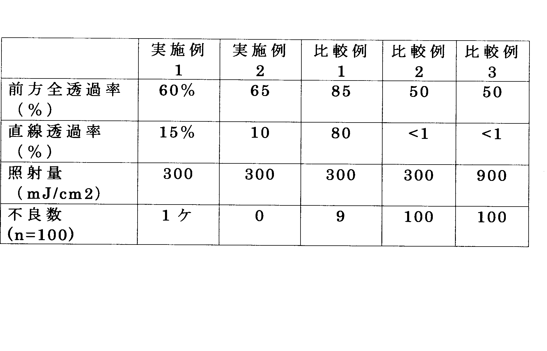
- the average value of the front total light transmittance at a wavelength of 200 to 400 nm of the obtained translucent alumina substrate was measured and found to be 60%, and the average value of linear transmittance was 15%.
- the polycrystalline translucent alumina constituting the handle substrate had an alumina purity of 99.9%.
- this substrate was polished to a thickness of 0.6 mm using GC (green carbon) abrasive grains, diamond abrasive grains, and CMP liquid in this order to obtain a base material 2.
- GC green carbon
- a single crystal Si substrate having a diameter of 4 inches and a thickness of 250 ⁇ m was prepared. Then, the single crystal Si substrate and the base material 2 described above were bonded together by direct bonding by plasma activation. Both substrates used for bonding were subjected to a plasma treatment with nitrogen, and then the surface particles were removed by a water washing treatment. By pressing the end portions of the two substrates and bringing them into close contact with each other, the pressed portions were bonded and the bonding propagated to the entire surface. This phenomenon is observed when the surfaces of the substrates are polished very smoothly because the bonding is automatically advanced by the force (attractive force between the surfaces) that the two substrates attract each other.
- the single crystal Si substrate side was ground with a grinder until the thickness reached 20 ⁇ m, and then lapped using a 1 ⁇ m diamond abrasive and a tin surface plate until the thickness reached 3 ⁇ m. .
- it was polished with colloidal silica and a urethane pad to a thickness of 0.2 ⁇ m.
- annealing treatment was performed at 300 ° C. to obtain a composite substrate of the base material 2 and the donor substrate 3.
- a single-crystal Si substrate as a supporting substrate 6 was bonded to the main surface on the circuit 4 side of the semiconductor circuit substrate thus obtained with an ultraviolet curable resin.
- the back surface 2b side of the semiconductor circuit board was ground with a grinder until the thickness of the semiconductor circuit board became 120 ⁇ m. Thereafter, dicing grooves 9 were formed so as to have a size of 1 mm ⁇ 1 mm according to the formed circuit 4.
- Example 2 A composite substrate was produced in the same manner as in Example 1. However, when the average value of the front total light transmittance of the obtained translucent alumina substrate at a wavelength of 200 to 400 nm was measured, it was 65%, and the average value of the linear transmittance was 10%. The polycrystalline translucent alumina constituting the handle substrate had an alumina purity of 99.9%. However, in order to change the front total light transmittance and the linear transmittance, the firing temperature was changed to 1710 ° C., and the annealing temperature and time were changed to 1710 ° C. ⁇ 12 hr.
- Example 1 In the same manner as in Example 1, the semiconductor circuit substrate and the supporting substrate were bonded with an ultraviolet curable resin, and the ultraviolet curable resin was cured, and 100 semiconductor circuit substrates 10 were separated from the supporting substrate.
- the handle substrate is single crystal sapphire
- the average value of the front total light transmittance in the wavelength range of 200 to 400 nm is 85%
- Example 2 In the same manner as in Example 1, the semiconductor circuit substrate and the supporting substrate were bonded with an ultraviolet curable resin, and the ultraviolet curable resin was cured, and 100 semiconductor circuit substrates 10 were separated from the supporting substrate.
- the handle substrate is made of alumina (99.5% purity)
- the average value of the front total light transmittance in the wavelength range of 200 to 400 nm is 50%
- the straight line in the wavelength range of 200 to 400 nm is 1% or less.
- Comparative Example 3 In Comparative Example 2, the ultraviolet irradiation time was extended. That is, UV light having a center wavelength of 365 nm was irradiated from the handle substrate 2A side at 900 mJ / cm 2 , but the UV curable resin 5 was not cured, and the cut pieces of each semiconductor circuit substrate 10 were peeled off from the support substrate 6. I could not.
- Table 1 The results are summarized in Table 1.
Landscapes
- Chemical & Material Sciences (AREA)
- Engineering & Computer Science (AREA)
- Ceramic Engineering (AREA)
- Organic Chemistry (AREA)
- Materials Engineering (AREA)
- Structural Engineering (AREA)
- Manufacturing & Machinery (AREA)
- Inorganic Chemistry (AREA)
- Life Sciences & Earth Sciences (AREA)
- Geology (AREA)
- Adhesives Or Adhesive Processes (AREA)
- Crystallography & Structural Chemistry (AREA)
- Container, Conveyance, Adherence, Positioning, Of Wafer (AREA)
- Thin Film Transistor (AREA)
- Crystals, And After-Treatments Of Crystals (AREA)
- Mechanical Treatment Of Semiconductor (AREA)
- Polishing Bodies And Polishing Tools (AREA)
Abstract
Description
ハンドル基板が多結晶透光性アルミナからなり、多結晶透光性アルミナのアルミナ純度が99.9%以上であり、多結晶透光性アルミナの200~400nmの波長範囲における前方全光線透過率の平均値が60%以上であり、多結晶透光性アルミナの200~400nmの波長範囲における直線透過率の平均値が15%以下であることを特徴とする。
多結晶透光性アルミナからなり、接合面と対向面とを有する基材、この基材の接合面に対して接合されているドナー基板、および前記ドナー基板上に設けられている回路を有する部品を得る工程であって、前記多結晶透光性アルミナのアルミナ純度が99.9%以上であり、前記多結晶透光性アルミナの200~400nmの波長範囲における前方全光線透過率の平均値が60%以上であり、前記多結晶透光性アルミナの200~400nmの波長範囲における直線透過率の平均値が15%以下である工程;
前記基材を前記対向面側から加工し、前記基材の厚さを小さくすることによって前記ハンドル基板を形成する工程;および
前記ドナー基板と支持基板との間に紫外線硬化型接着剤を介在させた状態で、200~400nmの波長範囲の紫外線を前記ハンドル基板側から前記紫外線硬化型樹脂へと照射することによって紫外線硬化型樹脂を硬化させることを特徴とする。
図1(a)に示すように、多結晶透光性アルミナからなる基材2を準備する。基材2の一対の主面のうち一方は接合面2aであり、他方は対向面2bである。基材2の接合面2aにドナー基板3を接合し、ドナー基板3上に回路4を形成する。次いで、ドナー基板3と別体の支持基板6との間に紫外線硬化型樹脂5を介在させることで、両者を粘着させ、部品1を作製する。
(半導体用複合基板)
本発明の複合基板は、プロジェクター用発光素子、高周波デバイス、高性能レーザー、パワーデバイス、ロジックICなどに利用できる。
複合基板は、本発明のハンドル基板と、ドナー基板とを含む。
ドナー基板の材質は、特に限定されないが、好ましくは、シリコン、窒化アルミニウム、窒化ガリウム、酸化亜鉛及びダイアモンドからなる群から選択される。ドナー基板の厚さは、特に限定されないが、通常のSEMI/JEITA規格近傍のものがハンドリングの関係から扱いやすい。
ハンドル基板の厚さは、特に限定されないが、通常のSEMI/JEITA規格近傍のものがハンドリングの関係から扱いやすい。具体的には、ハンドル基板の厚さは、直径が100mmのウェハの場合は525μm、直径150mmの場合は625μm、直径200mmの場合は725μm、直径300mmの場合は775μmとすることが好ましい。また、ハンドル基板にはキャビティを設けることもできる。
前方全光線透過率=100×(測定した光の強度)/(光源の強度)
基本的には前方全光線透過率と同様に測定する。ただし、図5に示すように、試料Sと積分球41の距離を80mmと離し、積分球41の開口部の寸法をφ10mmとし、試料Sから直線方向に開口部を通過した光のみを集め、その光強度を測定する。
また、本明細書における紫外線は、波長200以上、400nm以下の光線を意味する。
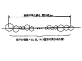
(1) 焼結体の断面を鏡面研磨、サーマルエッチングして粒界を際立たせた後、顕微鏡写真(100~200倍)を撮影し、単位長さの直線が横切る粒子の数を数える。これを異なる3箇所について実施する。なお、単位長さは500μm~1000μmの範囲とする。
(2) 実施した3箇所の粒子の個数の平均をとる。
(3) 下記の式により、平均粒径を算出する。
[算出式]
D=(4/π)×(L/n)
[D:平均粒径、L:直線の単位長さ、n:3箇所の粒子の個数の平均]
平均粒径の算出例を図6に示す。異なる3箇所の位置において、それぞれ単位長さ(例えば500μm)の直線が横切る粒子の個数が22、23、19としたとき、平均粒径Dは、上記算出式により、
D=(4/π)×[500/{(22+23+19)/3}]=29.9μm
となる。
なお、ここでいう平均粒径とはSEM写真(倍率:X30000。任意の2視野)上における2次凝集粒子を除く1次粒子の(最長軸長+最短軸長)/2の値のn=500平均値のことである。
(1) セラミック粉体とともに、結合剤となるポリビニルブチラール樹脂(PVB樹脂)、または、アクリル樹脂を、可塑剤、分散剤と共に分散媒中に分散してスラリーを調製し、ドクターブレード法にて、テープ状に成形した後、分散媒を乾燥させてスラリーを固化させる。
(2) 得られたテープを複数枚積み重ね、プレス積層またはCIP積層することで所望の厚みの基板形状の成形体を得る。
更に、アニール温度は焼成時の最高温度+0~100℃の範囲であることが好ましい。
ハンドル基板とドナー基板との接合に用いられる技術としては、特に限定される訳ではないが、例えば表面活性化による直接接合や、接着層を用いた基板接合技術が用いられる。
ドナー基板上の回路は、通常のフォトリソグラフィー法などによって形成することができる。また、回路は、貴金属の細線の他、はんだバンプや印刷電極などの各種電子素子を含む。
支持基板6の材質はシリコン、ガラス、石英、またはアルミナ、SiC、ジルコニア、窒化アルミ等の各種セラミックとすることができるが、平滑加工のし易さ、熱膨張マッチング、コストの観点からシリコン、ガラスが好ましい。
紫外線硬化型樹脂としては、具体的には、(i)アクリル系粘着剤、飽和コポリエステルなどの粘着剤(高分子弾性体)、(ii)紫外線硬化性成分、(iii)光重合開始剤、及び必要に応じて、架橋剤、粘着付与剤、可塑剤、充填剤、老化防止剤、着色剤などの慣用の添加剤を含む組成物が挙げられる。
以下の成分を混合したスラリーを調製した。
(原料粉末)
・比表面積3.5~4.5m2/g、平均一次粒子径0.35~0.45μmのα-アルミナ粉末
100重量部
・MgO(マグネシア) 250pppm
・ZrO2(ジルコニア) 400ppm
・Y2O3(イットリア) 15ppm
(分散媒)
・2-エチルヘキサノール 45重量部
(結合剤)
・PVB樹脂 4重量部
(分散剤)
・高分子界面活性剤 3重量部
(可塑剤)
・DOP 0.1重量部
実施例1と同様にして複合基板を作製した。ただし、得られた透光性アルミナ基板の波長200~400nmの前方全光線透過率の平均値を測定したところ、65%であり、直線透過率の平均値は10%であった。ハンドル基板を構成する多結晶透光性アルミナのアルミナ純度が99.9%であった。ただし、前方全光線透過率、直線透過率を変えるために、焼成温度を1710℃とし、アニール温度および時間を1710℃×12hrに変更した。
実施例1と同様にして半導体回路基板と支持基板とを紫外線硬化型樹脂によって接着し、紫外線硬化型樹脂を硬化させて支持基板から半導体回路基板10を100個剥離させた。ただし、本例においては、ハンドル基板は単結晶サファイアであり、200~400nmの波長範囲における前方全光線透過率の平均値が85%であり、200~400nmの波長範囲における直線透過率の平均値が80%である。
実施例1と同様にして半導体回路基板と支持基板とを紫外線硬化型樹脂によって接着し、紫外線硬化型樹脂を硬化させて支持基板から半導体回路基板10を100個剥離させた。ただし、本例においては、ハンドル基板はアルミナ(99.5%純度)であり、200~400nmの波長範囲における前方全光線透過率の平均値が50%であり、200~400nmの波長範囲における直線透過率の平均値が1%以下である。
比較例2において、紫外線の照射時間を延ばした。すなわち、ハンドル基板2A側から中心波長365nmの紫外線を900mJ/cm2照射したが、紫外線硬化型樹脂5は硬化せず支持基板6から、切断された各半導体回路基板10の個片を剥離することができなかった。上記の結果を表1にまとめた。
Claims (7)
- 半導体用複合基板のハンドル基板であって、
前記ハンドル基板が多結晶透光性アルミナからなり、前記多結晶透光性アルミナのアルミナ純度が99.9%以上であり、前記多結晶透光性アルミナの200~400nmの波長範囲における前方全光線透過率の平均値が60%以上であり、前記多結晶透光性アルミナの200~400nmの波長範囲における直線透過率の平均値が15%以下であることを特徴とする、ハンドル基板。 - 請求項1記載のハンドル基板、および前記ハンドル基板の接合面に対して接合されているドナー基板を有することを特徴とする、半導体用複合基板。
- 前記ドナー基板が単結晶シリコンからなることを特徴とする、請求項2記載の複合基板。
- 請求項2または3記載の半導体用複合基板、および前記ドナー基板上に設けられている回路を有することを特徴とする、半導体回路基板。
- ハンドル基板、前記ハンドル基板の接合面に対して接合されているドナー基板、および前記ドナー基板上に設けられている回路を有する半導体回路基板を製造する方法であって、
多結晶透光性アルミナからなり、接合面と対向面とを有する基材、この基材の接合面に対して接合されているドナー基板、および前記ドナー基板上に設けられている回路を有する部品を得る工程であって、前記多結晶透光性アルミナのアルミナ純度が99.9%以上であり、前記多結晶透光性アルミナの200~400nmの波長範囲における前方全光線透過率の平均値が60%以上であり、前記多結晶透光性アルミナの200~400nmの波長範囲における直線透過率の平均値が15%以下である工程;
前記基材を前記対向面側から加工し、前記基材の厚さを小さくすることによって前記ハンドル基板を形成する工程;および
前記ドナー基板と支持基板との間に紫外線硬化型樹脂を介在させた状態で、200~400nmの波長範囲の紫外線を前記ハンドル基板側から前記紫外線硬化型樹脂へと照射することによって前記紫外線硬化型樹脂を硬化させることを特徴とする、半導体回路基板の製造方法。 - 前記紫外線硬化型樹脂を硬化させた後、前記支持基板を前記半導体回路基板から剥離させる剥離工程を有することを特徴とする、請求項5記載の方法。
- 前記ドナー基板が単結晶シリコンからなることを特徴とする、請求項5または6記載の方法。
Priority Applications (5)
| Application Number | Priority Date | Filing Date | Title |
|---|---|---|---|
| EP14873693.7A EP2978009B1 (en) | 2013-12-25 | 2014-12-16 | Handle substrate, composite substrate for semiconductor, and semiconductor circuit board and method for manufacturing same |
| CN201480019693.7A CN105074870B (zh) | 2013-12-25 | 2014-12-16 | 操作基板、半导体用复合基板、半导体电路基板及其制造方法 |
| JP2015518488A JP5781254B1 (ja) | 2013-12-25 | 2014-12-16 | ハンドル基板、半導体用複合基板、半導体回路基板およびその製造方法 |
| KR1020157021527A KR101570958B1 (ko) | 2013-12-25 | 2014-12-16 | 핸들 기판, 반도체용 복합 기판, 반도체 회로 기판 및 그 제조 방법 |
| US14/853,011 US9425083B2 (en) | 2013-12-25 | 2015-09-14 | Handle substrate, composite substrate for semiconductor, and semiconductor circuit board and method for manufacturing the same |
Applications Claiming Priority (2)
| Application Number | Priority Date | Filing Date | Title |
|---|---|---|---|
| JP2013267455 | 2013-12-25 | ||
| JP2013-267455 | 2013-12-25 |
Related Child Applications (1)
| Application Number | Title | Priority Date | Filing Date |
|---|---|---|---|
| US14/853,011 Continuation US9425083B2 (en) | 2013-12-25 | 2015-09-14 | Handle substrate, composite substrate for semiconductor, and semiconductor circuit board and method for manufacturing the same |
Publications (1)
| Publication Number | Publication Date |
|---|---|
| WO2015098609A1 true WO2015098609A1 (ja) | 2015-07-02 |
Family
ID=53478473
Family Applications (1)
| Application Number | Title | Priority Date | Filing Date |
|---|---|---|---|
| PCT/JP2014/083209 Ceased WO2015098609A1 (ja) | 2013-12-25 | 2014-12-16 | ハンドル基板、半導体用複合基板、半導体回路基板およびその製造方法 |
Country Status (7)
| Country | Link |
|---|---|
| US (1) | US9425083B2 (ja) |
| EP (1) | EP2978009B1 (ja) |
| JP (1) | JP5781254B1 (ja) |
| KR (1) | KR101570958B1 (ja) |
| CN (1) | CN105074870B (ja) |
| TW (1) | TWI514441B (ja) |
| WO (1) | WO2015098609A1 (ja) |
Cited By (2)
| Publication number | Priority date | Publication date | Assignee | Title |
|---|---|---|---|---|
| EP3113211A4 (en) * | 2014-02-26 | 2017-10-11 | NGK Insulators, Ltd. | Handle substrate of composite substrate for semiconductor |
| JP2017535967A (ja) * | 2015-07-14 | 2017-11-30 | ゴルテック.インク | フリップダイの組立方法、製造方法、装置及び電子機器 |
Families Citing this family (7)
| Publication number | Priority date | Publication date | Assignee | Title |
|---|---|---|---|---|
| EP3010051B1 (en) * | 2013-06-12 | 2020-01-08 | NGK Insulators, Ltd. | Window material for ultraviolet-ray-emitting element and method for producing same |
| US10446442B2 (en) | 2016-12-21 | 2019-10-15 | Globalfoundries Inc. | Integrated circuit chip with molding compound handler substrate and method |
| JP6980421B2 (ja) * | 2017-06-16 | 2021-12-15 | 株式会社ディスコ | ウエーハの加工方法 |
| CN113544819B (zh) * | 2019-03-22 | 2024-01-05 | 日本碍子株式会社 | 预固定基板、复合基板以及电子元件的剥离方法 |
| JP2025086063A (ja) * | 2023-11-27 | 2025-06-06 | タツモ株式会社 | 半導体デバイスの製造方法 |
| JP2025086064A (ja) * | 2023-11-27 | 2025-06-06 | タツモ株式会社 | 半導体デバイスの製造方法 |
| CN118573145B (zh) * | 2024-08-01 | 2024-12-20 | 泉州市三安集成电路有限公司 | 支撑基板及其制备方法、复合基板、电子器件和模块 |
Citations (11)
| Publication number | Priority date | Publication date | Assignee | Title |
|---|---|---|---|---|
| JPH05160240A (ja) | 1991-12-03 | 1993-06-25 | Toshiba Ceramics Co Ltd | ダミーウェーハ |
| JPH08512432A (ja) | 1993-07-12 | 1996-12-24 | ペレグリン・セミコンダクター・コーポレイション | 単一の超薄膜シリコン・オン・サファイアチップ上の高周波ワイヤレス通信システム |
| JP2003224042A (ja) | 2001-12-21 | 2003-08-08 | Soi Tec Silicon On Insulator Technologies | 半導体薄層の移し換え方法とそれに使用するドナーウエハの製造方法 |
| JP2005159155A (ja) * | 2003-11-27 | 2005-06-16 | Three M Innovative Properties Co | 半導体チップの製造方法 |
| JP2005191550A (ja) | 2003-12-01 | 2005-07-14 | Tokyo Ohka Kogyo Co Ltd | 基板の貼り付け方法 |
| JP2008288556A (ja) | 2007-04-18 | 2008-11-27 | Shin Etsu Chem Co Ltd | 貼り合わせ基板の製造方法 |
| JP2010258341A (ja) | 2009-04-28 | 2010-11-11 | Mitsubishi Plastics Inc | ダイシング用粘着シート |
| WO2010128666A1 (ja) | 2009-05-07 | 2010-11-11 | 信越化学工業株式会社 | 貼り合わせウェーハの製造方法 |
| JP2010278341A (ja) | 2009-05-29 | 2010-12-09 | Shin-Etsu Chemical Co Ltd | 貼り合わせsos基板 |
| WO2013187410A1 (ja) * | 2012-06-13 | 2013-12-19 | 日本碍子株式会社 | 複合基板 |
| WO2014013980A1 (ja) | 2012-07-18 | 2014-01-23 | 日本碍子株式会社 | 複合ウェハー及びその製法 |
Family Cites Families (13)
| Publication number | Priority date | Publication date | Assignee | Title |
|---|---|---|---|---|
| EP0567095B1 (en) * | 1992-04-22 | 1996-07-03 | Sumitomo Chemical Company, Limited | Translucent polycrystalline alumina and process for producing the same |
| US5864162A (en) | 1993-07-12 | 1999-01-26 | Peregrine Seimconductor Corporation | Apparatus and method of making a self-aligned integrated resistor load on ultrathin silicon on sapphire |
| US5587346A (en) * | 1995-06-16 | 1996-12-24 | Osram Sylvania, Inc. | Translucent polycrystalline alumina |
| JP3783445B2 (ja) * | 1999-01-29 | 2006-06-07 | 住友化学株式会社 | 透光性アルミナ焼結体の製造方法およびその用途 |
| CA2308933C (en) * | 1999-05-19 | 2008-07-22 | Ngk Spark Plug Co., Ltd. | Translucent polycrystalline ceramic and method for making same |
| US6878456B2 (en) * | 2001-12-28 | 2005-04-12 | 3M Innovative Properties Co. | Polycrystalline translucent alumina-based ceramic material, uses, and methods |
| CN100420651C (zh) * | 2005-11-03 | 2008-09-24 | 韩敏芳 | 具有高线性透光率的亚微米晶粒透明氧化铝陶瓷 |
| US8088670B2 (en) | 2007-04-18 | 2012-01-03 | Shin-Etsu Chemical Co., Ltd. | Method for manufacturing bonded substrate with sandblast treatment |
| CN102992739A (zh) * | 2012-12-17 | 2013-03-27 | 江苏大学 | 一种多功能透明氧化铝陶瓷的制备方法 |
| TWI629753B (zh) * | 2013-04-26 | 2018-07-11 | Ngk Insulators, Ltd. | 半導體用複合基板之操作基板 |
| WO2015008694A1 (ja) * | 2013-07-18 | 2015-01-22 | 日本碍子株式会社 | 半導体用複合基板のハンドル基板 |
| KR101597501B1 (ko) * | 2014-01-06 | 2016-02-24 | 엔지케이 인슐레이터 엘티디 | 핸들 기판 및 반도체용 복합 웨이퍼 |
| JP6076486B2 (ja) * | 2014-02-26 | 2017-02-08 | 日本碍子株式会社 | 半導体用複合基板のハンドル基板 |
-
2014
- 2014-12-16 KR KR1020157021527A patent/KR101570958B1/ko not_active Expired - Fee Related
- 2014-12-16 EP EP14873693.7A patent/EP2978009B1/en not_active Not-in-force
- 2014-12-16 JP JP2015518488A patent/JP5781254B1/ja not_active Expired - Fee Related
- 2014-12-16 CN CN201480019693.7A patent/CN105074870B/zh not_active Expired - Fee Related
- 2014-12-16 WO PCT/JP2014/083209 patent/WO2015098609A1/ja not_active Ceased
- 2014-12-22 TW TW103144719A patent/TWI514441B/zh not_active IP Right Cessation
-
2015
- 2015-09-14 US US14/853,011 patent/US9425083B2/en not_active Expired - Fee Related
Patent Citations (11)
| Publication number | Priority date | Publication date | Assignee | Title |
|---|---|---|---|---|
| JPH05160240A (ja) | 1991-12-03 | 1993-06-25 | Toshiba Ceramics Co Ltd | ダミーウェーハ |
| JPH08512432A (ja) | 1993-07-12 | 1996-12-24 | ペレグリン・セミコンダクター・コーポレイション | 単一の超薄膜シリコン・オン・サファイアチップ上の高周波ワイヤレス通信システム |
| JP2003224042A (ja) | 2001-12-21 | 2003-08-08 | Soi Tec Silicon On Insulator Technologies | 半導体薄層の移し換え方法とそれに使用するドナーウエハの製造方法 |
| JP2005159155A (ja) * | 2003-11-27 | 2005-06-16 | Three M Innovative Properties Co | 半導体チップの製造方法 |
| JP2005191550A (ja) | 2003-12-01 | 2005-07-14 | Tokyo Ohka Kogyo Co Ltd | 基板の貼り付け方法 |
| JP2008288556A (ja) | 2007-04-18 | 2008-11-27 | Shin Etsu Chem Co Ltd | 貼り合わせ基板の製造方法 |
| JP2010258341A (ja) | 2009-04-28 | 2010-11-11 | Mitsubishi Plastics Inc | ダイシング用粘着シート |
| WO2010128666A1 (ja) | 2009-05-07 | 2010-11-11 | 信越化学工業株式会社 | 貼り合わせウェーハの製造方法 |
| JP2010278341A (ja) | 2009-05-29 | 2010-12-09 | Shin-Etsu Chemical Co Ltd | 貼り合わせsos基板 |
| WO2013187410A1 (ja) * | 2012-06-13 | 2013-12-19 | 日本碍子株式会社 | 複合基板 |
| WO2014013980A1 (ja) | 2012-07-18 | 2014-01-23 | 日本碍子株式会社 | 複合ウェハー及びその製法 |
Non-Patent Citations (1)
| Title |
|---|
| See also references of EP2978009A4 |
Cited By (2)
| Publication number | Priority date | Publication date | Assignee | Title |
|---|---|---|---|---|
| EP3113211A4 (en) * | 2014-02-26 | 2017-10-11 | NGK Insulators, Ltd. | Handle substrate of composite substrate for semiconductor |
| JP2017535967A (ja) * | 2015-07-14 | 2017-11-30 | ゴルテック.インク | フリップダイの組立方法、製造方法、装置及び電子機器 |
Also Published As
| Publication number | Publication date |
|---|---|
| EP2978009A1 (en) | 2016-01-27 |
| US20160005643A1 (en) | 2016-01-07 |
| US9425083B2 (en) | 2016-08-23 |
| TW201537617A (zh) | 2015-10-01 |
| CN105074870A (zh) | 2015-11-18 |
| CN105074870B (zh) | 2016-12-07 |
| JP5781254B1 (ja) | 2015-09-16 |
| KR101570958B1 (ko) | 2015-11-20 |
| JPWO2015098609A1 (ja) | 2017-03-23 |
| EP2978009A4 (en) | 2016-12-28 |
| TWI514441B (zh) | 2015-12-21 |
| EP2978009B1 (en) | 2018-03-21 |
| KR20150097812A (ko) | 2015-08-26 |
Similar Documents
| Publication | Publication Date | Title |
|---|---|---|
| JP5781254B1 (ja) | ハンドル基板、半導体用複合基板、半導体回路基板およびその製造方法 | |
| KR102222089B1 (ko) | 복합 기판, 반도체 디바이스 및 반도체 디바이스의 제법 | |
| KR101142000B1 (ko) | 정전척 | |
| JP6076486B2 (ja) | 半導体用複合基板のハンドル基板 | |
| CN112802790B (zh) | 保护部件的设置方法和保护部件的制造方法 | |
| JP5697813B1 (ja) | 半導体用複合基板のハンドル基板 | |
| KR102188440B1 (ko) | 반도체용 복합 기판의 핸들 기판 | |
| KR102588785B1 (ko) | 반도체 소자의 제조 방법 | |
| WO2015102065A1 (ja) | ハンドル基板および半導体用複合ウエハー | |
| US20110290415A1 (en) | Apparatus and method for detaping an adhesive layer from the surface of ultra thin wafers | |
| KR101642671B1 (ko) | 반도체용 복합 기판의 핸들 기판 및 반도체용 복합 기판 | |
| CN115424918A (zh) | 一种碳化硅与氮化镓键合的超薄晶圆制作工艺 | |
| JP7430704B2 (ja) | 仮固定基板、複合基板および電子部品の剥離方法 | |
| TWI814872B (zh) | 暫時固定基板、暫時固定方法及電子構件的製造方法 |
Legal Events
| Date | Code | Title | Description |
|---|---|---|---|
| WWE | Wipo information: entry into national phase |
Ref document number: 201480019693.7 Country of ref document: CN |
|
| ENP | Entry into the national phase |
Ref document number: 2015518488 Country of ref document: JP Kind code of ref document: A |
|
| ENP | Entry into the national phase |
Ref document number: 20157021527 Country of ref document: KR Kind code of ref document: A |
|
| 121 | Ep: the epo has been informed by wipo that ep was designated in this application |
Ref document number: 14873693 Country of ref document: EP Kind code of ref document: A1 |
|
| WWE | Wipo information: entry into national phase |
Ref document number: 2014873693 Country of ref document: EP |
|
| NENP | Non-entry into the national phase |
Ref country code: DE |