WO2015102364A1 - Polariseur réfléchissant de type à dispersion aléatoire - Google Patents
Polariseur réfléchissant de type à dispersion aléatoire Download PDFInfo
- Publication number
- WO2015102364A1 WO2015102364A1 PCT/KR2014/013030 KR2014013030W WO2015102364A1 WO 2015102364 A1 WO2015102364 A1 WO 2015102364A1 KR 2014013030 W KR2014013030 W KR 2014013030W WO 2015102364 A1 WO2015102364 A1 WO 2015102364A1
- Authority
- WO
- WIPO (PCT)
- Prior art keywords
- reflective polarizer
- group
- layer
- dispersions
- dispersion
- Prior art date
- Legal status (The legal status is an assumption and is not a legal conclusion. Google has not performed a legal analysis and makes no representation as to the accuracy of the status listed.)
- Ceased
Links
Images




Classifications
-
- G—PHYSICS
- G02—OPTICS
- G02B—OPTICAL ELEMENTS, SYSTEMS OR APPARATUS
- G02B5/00—Optical elements other than lenses
- G02B5/30—Polarising elements
- G02B5/3008—Polarising elements comprising dielectric particles, e.g. birefringent crystals embedded in a matrix
-
- B—PERFORMING OPERATIONS; TRANSPORTING
- B29—WORKING OF PLASTICS; WORKING OF SUBSTANCES IN A PLASTIC STATE IN GENERAL
- B29D—PRODUCING PARTICULAR ARTICLES FROM PLASTICS OR FROM SUBSTANCES IN A PLASTIC STATE
- B29D11/00—Producing optical elements, e.g. lenses or prisms
- B29D11/00009—Production of simple or compound lenses
- B29D11/00278—Lenticular sheets
-
- B—PERFORMING OPERATIONS; TRANSPORTING
- B29—WORKING OF PLASTICS; WORKING OF SUBSTANCES IN A PLASTIC STATE IN GENERAL
- B29D—PRODUCING PARTICULAR ARTICLES FROM PLASTICS OR FROM SUBSTANCES IN A PLASTIC STATE
- B29D11/00—Producing optical elements, e.g. lenses or prisms
- B29D11/00634—Production of filters
- B29D11/00644—Production of filters polarizing
-
- G—PHYSICS
- G02—OPTICS
- G02B—OPTICAL ELEMENTS, SYSTEMS OR APPARATUS
- G02B27/00—Optical systems or apparatus not provided for by any of the groups G02B1/00 - G02B26/00, G02B30/00
- G02B27/28—Optical systems or apparatus not provided for by any of the groups G02B1/00 - G02B26/00, G02B30/00 for polarising
- G02B27/283—Optical systems or apparatus not provided for by any of the groups G02B1/00 - G02B26/00, G02B30/00 for polarising used for beam splitting or combining
-
- G—PHYSICS
- G02—OPTICS
- G02B—OPTICAL ELEMENTS, SYSTEMS OR APPARATUS
- G02B5/00—Optical elements other than lenses
- G02B5/02—Diffusing elements; Afocal elements
- G02B5/0273—Diffusing elements; Afocal elements characterized by the use
- G02B5/0294—Diffusing elements; Afocal elements characterized by the use adapted to provide an additional optical effect, e.g. anti-reflection or filter
-
- G—PHYSICS
- G02—OPTICS
- G02B—OPTICAL ELEMENTS, SYSTEMS OR APPARATUS
- G02B5/00—Optical elements other than lenses
- G02B5/30—Polarising elements
- G02B5/3083—Birefringent or phase retarding elements
-
- G—PHYSICS
- G02—OPTICS
- G02F—OPTICAL DEVICES OR ARRANGEMENTS FOR THE CONTROL OF LIGHT BY MODIFICATION OF THE OPTICAL PROPERTIES OF THE MEDIA OF THE ELEMENTS INVOLVED THEREIN; NON-LINEAR OPTICS; FREQUENCY-CHANGING OF LIGHT; OPTICAL LOGIC ELEMENTS; OPTICAL ANALOGUE/DIGITAL CONVERTERS
- G02F1/00—Devices or arrangements for the control of the intensity, colour, phase, polarisation or direction of light arriving from an independent light source, e.g. switching, gating or modulating; Non-linear optics
- G02F1/01—Devices or arrangements for the control of the intensity, colour, phase, polarisation or direction of light arriving from an independent light source, e.g. switching, gating or modulating; Non-linear optics for the control of the intensity, phase, polarisation or colour
- G02F1/13—Devices or arrangements for the control of the intensity, colour, phase, polarisation or direction of light arriving from an independent light source, e.g. switching, gating or modulating; Non-linear optics for the control of the intensity, phase, polarisation or colour based on liquid crystals, e.g. single liquid crystal display cells
- G02F1/133—Constructional arrangements; Operation of liquid crystal cells; Circuit arrangements
- G02F1/1333—Constructional arrangements; Manufacturing methods
- G02F1/1335—Structural association of cells with optical devices, e.g. polarisers or reflectors
- G02F1/133528—Polarisers
-
- G—PHYSICS
- G02—OPTICS
- G02F—OPTICAL DEVICES OR ARRANGEMENTS FOR THE CONTROL OF LIGHT BY MODIFICATION OF THE OPTICAL PROPERTIES OF THE MEDIA OF THE ELEMENTS INVOLVED THEREIN; NON-LINEAR OPTICS; FREQUENCY-CHANGING OF LIGHT; OPTICAL LOGIC ELEMENTS; OPTICAL ANALOGUE/DIGITAL CONVERTERS
- G02F1/00—Devices or arrangements for the control of the intensity, colour, phase, polarisation or direction of light arriving from an independent light source, e.g. switching, gating or modulating; Non-linear optics
- G02F1/01—Devices or arrangements for the control of the intensity, colour, phase, polarisation or direction of light arriving from an independent light source, e.g. switching, gating or modulating; Non-linear optics for the control of the intensity, phase, polarisation or colour
- G02F1/13—Devices or arrangements for the control of the intensity, colour, phase, polarisation or direction of light arriving from an independent light source, e.g. switching, gating or modulating; Non-linear optics for the control of the intensity, phase, polarisation or colour based on liquid crystals, e.g. single liquid crystal display cells
- G02F1/133—Constructional arrangements; Operation of liquid crystal cells; Circuit arrangements
- G02F1/1333—Constructional arrangements; Manufacturing methods
- G02F1/1335—Structural association of cells with optical devices, e.g. polarisers or reflectors
- G02F1/133528—Polarisers
- G02F1/133536—Reflective polarizers
-
- G—PHYSICS
- G02—OPTICS
- G02B—OPTICAL ELEMENTS, SYSTEMS OR APPARATUS
- G02B5/00—Optical elements other than lenses
- G02B5/02—Diffusing elements; Afocal elements
- G02B5/0205—Diffusing elements; Afocal elements characterised by the diffusing properties
- G02B5/021—Diffusing elements; Afocal elements characterised by the diffusing properties the diffusion taking place at the element's surface, e.g. by means of surface roughening or microprismatic structures
- G02B5/0215—Diffusing elements; Afocal elements characterised by the diffusing properties the diffusion taking place at the element's surface, e.g. by means of surface roughening or microprismatic structures the surface having a regular structure
-
- G—PHYSICS
- G02—OPTICS
- G02B—OPTICAL ELEMENTS, SYSTEMS OR APPARATUS
- G02B5/00—Optical elements other than lenses
- G02B5/02—Diffusing elements; Afocal elements
- G02B5/0205—Diffusing elements; Afocal elements characterised by the diffusing properties
- G02B5/021—Diffusing elements; Afocal elements characterised by the diffusing properties the diffusion taking place at the element's surface, e.g. by means of surface roughening or microprismatic structures
- G02B5/0221—Diffusing elements; Afocal elements characterised by the diffusing properties the diffusion taking place at the element's surface, e.g. by means of surface roughening or microprismatic structures the surface having an irregular structure
-
- G—PHYSICS
- G02—OPTICS
- G02B—OPTICAL ELEMENTS, SYSTEMS OR APPARATUS
- G02B5/00—Optical elements other than lenses
- G02B5/02—Diffusing elements; Afocal elements
- G02B5/0205—Diffusing elements; Afocal elements characterised by the diffusing properties
- G02B5/021—Diffusing elements; Afocal elements characterised by the diffusing properties the diffusion taking place at the element's surface, e.g. by means of surface roughening or microprismatic structures
- G02B5/0231—Diffusing elements; Afocal elements characterised by the diffusing properties the diffusion taking place at the element's surface, e.g. by means of surface roughening or microprismatic structures the surface having microprismatic or micropyramidal shape
Definitions
- the present invention relates to a randomly distributed reflective polarizer, and more particularly, to provide a randomly distributed reflective polarizer capable of maximizing brightness while minimizing light loss.
- LCD liquid crystal display
- PDP plasma display
- FED field emission display
- ELD electroluminescent display
- LCD displays are currently expanding their range of use, including notebooks, personal computer monitors, LCD TVs, automobiles, and airplanes, accounting for about 80% of the flat panel market, and are booming to date due to a sharp increase in LCD demand worldwide.
- liquid crystal displays arrange a liquid crystal and an electrode matrix between a pair of light absorbing optical films.
- the liquid crystal portion has an optical state that is changed accordingly by moving the liquid crystal portion by an electric field generated by applying a voltage to two electrodes. This process displays an image of a 'pixel' carrying information using polarization in a specific direction.
- liquid crystal displays include a front optical film and a back optical film that induce polarization.
- the optical film used in such a liquid crystal display does not necessarily have high utilization efficiency of light emitted from the backlight. This is because 50% or more of the light emitted from the backlight is absorbed by the back side optical film (absorption type polarizing film).
- a reflective polarizer is provided between the optical cavity and the liquid crystal assembly.
- FIG. 1 is a view showing the optical principle of a conventional reflective polarizer. Specifically, P-polarized light from the optical cavity to the liquid crystal assembly passes through the reflective polarizer to the liquid crystal assembly, and S-polarized light is reflected from the reflective polarizer to the optical cavity and then polarized light on the diffuse reflection surface of the optical cavity. The direction is reflected in a randomized state and then transmitted back to the reflective polarizer so that S-polarized light is converted into P-polarized light which can pass through the polarizer of the liquid crystal assembly, and then passed through the reflective polarizer to be transmitted to the liquid crystal assembly.
- the selective reflection of S-polarized light and the transmission of P-polarized light with respect to the incident light of the reflective polarizer are based on the refractive index of each optical layer in a state where an optical layer on a plate having anisotropic refractive index and an optical layer on a plate having an isotropic refractive index are laminated alternately. It is made by the optical thickness setting of each optical layer and the refractive index change of the optical layer according to the difference and the stretching process of the stacked optical layers.
- the light incident to the reflective polarizer repeats the reflection of S-polarized light and the transmission of P-polarized light while passing through each optical layer, and eventually only the P-polarized light of the incident polarized light is transmitted to the liquid crystal assembly.
- the reflected S-polarized light is reflected in a state in which the polarization state is randomized at the diffuse reflection surface of the optical cavity and is transmitted to the reflective polarizer again. As a result, power loss can be reduced together with the loss of light generated from the light source.
- the conventional reflective polarizer has an optical thickness and a refractive index between the optical layers that can be optimized for selective reflection and transmission of incident polarization by alternately stacking isotropic optical layers and anisotropic optical layers having different refractive indices. Since it is manufactured so as to have it, there existed a problem that the manufacturing process of a reflective polarizer was complicated. In particular, since each optical layer of the reflective polarizer has a flat plate structure, it is necessary to separate P-polarized light and S-polarized light in response to a wide range of incident angles of incident polarization, so that the number of optical layers is excessively increased and the production cost is exponentially increased. There was a growing problem. In addition, due to the structure in which the number of laminated layers of the optical layer is excessively formed, there is a problem that the optical performance decrease due to light loss.
- FIG. 2 is a cross-sectional view of a conventional multilayer reflective polarizer (DBEF).
- the multilayer reflective polarizer has skin layers 9 and 10 formed on both sides of the substrate 8.
- Substrate 8 is divided into four groups (1, 2, 3, 4), each group of which isotropic and anisotropic layers are alternately stacked to form approximately 200 layers.
- separate adhesive layers 5, 6, 7 for bonding them are formed between the four groups 1, 2, 3, 4 forming the substrate 8.
- each group since each group has a very thin thickness of about 200 layers, each group may be damaged when co-extrusion of these groups individually, so the groups often include a protective layer (PBL). In this case, there is a problem that the thickness of the substrate becomes thick and the manufacturing cost increases.
- PBL protective layer
- the thickness of the substrate is limited for slimming, when the adhesive layer is formed on the substrate and / or the skin layer, the substrate is reduced by the thickness thereof. there was. Furthermore, since the inside of the substrate and the substrate and the skin layer are bonded by an adhesive layer, there is a problem in that an interlayer peeling phenomenon occurs when an external force is applied, when a long time passes, or when the storage location is poor. In addition, in the process of attaching the adhesive layer, not only the defect rate is excessively high but also there is a problem in that offset interference with the light source occurs due to the formation of the adhesive layer.
- Skin layers 9 and 10 are formed on both sides of the substrate 8, and separate adhesive layers 11 and 12 are formed to bond them between the substrate 8 and the skin layers 9 and 10.
- peeling may occur due to incompatibility, and the birefringence on the stretching axis when the stretching process is performed due to the crystallinity of about 15% High risk of occurrence.
- the addition of the adhesive layer process results in a decrease in yield due to external foreign matters and process defects.
- the conventional method of manufacturing the multilayer reflective polarizer is briefly described. After co-extracting four groups having different average optical thicknesses to form a substrate separately, the four co-extruded four groups are stretched and then stretched. Four groups are glued together to form a substrate. This is because the peeling phenomenon occurs when the substrate is stretched after adhesive bonding. Thereafter, the skin layer is adhered to both surfaces of the substrate. After all, in order to make a multi-layered structure, a group of 209 layers is formed through the process of folding a 2-layered structure to form a 4-layered structure and a continuous folding type of multi-layered structure. It was difficult to form groups inside the multilayer in the process. As a result, four groups having different average optical thicknesses can be co-extruded separately and then bonded to each other.
- a reflective polarizer in which a dispersion is dispersed in which a birefringent polymer elongated in the longitudinal direction is arranged inside a substrate rather than a multilayer reflective polarizer is achieved.
- 3 is a perspective view of a reflective polarizer 20 including a rod-shaped polymer, in which the birefringent polymer 22 extending in the longitudinal direction is arranged in one direction in the substrate 21.
- the birefringent interface between the substrate 21 and the birefringent polymer 22 causes the light modulation effect to perform the function of the reflective polarizer.
- FIG. 4 is a cross-sectional view of a birefringent island-in-the-sea yarn included in the substrate, and the birefringent island-in-the-sea yarn may generate a light modulation effect at an optical modulation interface between the inner and sea portions of the inner portion, and thus, a very large number such as the birefringent polymer described above. Optical properties can be achieved even if the island-in-the-sea yarns are not disposed.
- the birefringent island-in-the-sea yarn is a fiber
- problems of compatibility, ease of handling, and adhesion with a substrate which is a polymer have arisen.
- the circular shape due to the circular shape, light scattering is induced, and thus the reflection polarization efficiency of the visible wavelength is reduced, and the polarization characteristic is lowered compared to the existing products, thereby limiting the luminance improvement.
- the voids cause the optical leakage due to light leakage, that is, light loss.
- a limitation occurs in the reflection and polarization characteristics due to the limitation of the layer configuration due to the organization of tissue in the form of a fabric.
- the scattered reflective polarizer the visible line is observed due to the space between the layers and the space between the dispersions.
- the present invention has been made to solve the above-described problem, the present invention is a random dispersion type that can maximize the brightness enhancement while wider viewing angle and minimize the light loss while improving the linear appearance compared to the conventional distributed reflective polarizer It is to provide a reflective polarizer.
- a plurality of dispersions are included in the substrate, the plurality of dispersions in the at least one axial direction with the substrate.
- the refractive index is different, and the aspect ratio of the short axis length to the major axis length is 1/2 or less, and the aspect ratio is 1/2 or less, based on the vertical cross section in the longitudinal direction of 80% or more of the plurality of dispersions contained in the substrate.
- dispersions are a group includes more than two different cross-sectional area, the cross-sectional area of the first group is 0.2 ⁇ 2.0 ⁇ m 2, and the cross-sectional area of the second group is at most 2 from 5.0 ⁇ m 2.0 ⁇ m 2, greater than the cross-sectional area of the third group 5.0 ⁇ m and 10.0 ⁇ m 2 or less from greater than 2, the randomly arranged core layer body 1 group dispersion, the dispersion of the second group and the third group of the dispersion of; provides a randomly distributed reflective polarizer comprising a.
- a random scattering reflective polarizer further comprising an integrated skin layer formed on at least one surface of the core layer.
- the number of dispersions of the third group of the dispersion having an aspect ratio of 1/2 or less may be 10% or more.
- the number of the first group of the dispersion having the aspect ratio of 1/2 or less may be 30 to 50%
- the number of the third group may be 10 to 30%
- the number of the second group in the dispersion having the aspect ratio of 1/2 or less may be 25 to 45%.
- the refractive index of the substrate and the dispersion may have a difference in refractive index of 0.05 or less in two axial directions, and the difference in refractive index of the other one axial direction may be 0.1 or more.
- the reflective polarizer may be drawn in at least one axial direction.
- it may comprise a structured surface layer formed on at least one side of the substrate.
- it may further include a primer layer for enhancing adhesion between the substrate and the structured surface layer.
- the structured surface layer may be a micropattern layer.
- the micropattern may be any one or more selected from the group consisting of prisms, lenticulars, microlenses, triangular pyramids, and pyramid patterns.
- (1) includes a plurality of dispersions inside the substrate, in order to transmit the first polarized light irradiated from the outside and reflect the second polarized light, the plurality of dispersions is the substrate And the refractive index is different in at least one axial direction, and at least 80% of the plurality of dispersions contained in the substrate have an aspect ratio of the short axis length to the major axis length of 1/2 or less based on the vertical section in the longitudinal direction, and the aspect ratio is not more than half the dispersion comprise at least three groups are different from the cross-sectional area, the cross-sectional area of the first group 2 0.2 ⁇ 2.0 ⁇ m, the cross-sectional area of the second group is less than a second 5.0 ⁇ m 2 from 2.0 ⁇ m , and 10.0 ⁇ m claim 2 or less from cross-sectional area is greater than 2 5.0 ⁇ m of the third group, the variance of the first group element, the dispersion of the second element group and the third randomly distributed comprising a
- the method may further include manufacturing a skin layer integrated on at least one surface of the core layer.
- a step (2) after the step (1) it may further comprise the step of forming a structured surface layer on at least one side of the substrate.
- it may further comprise the step of forming a primer layer for enhancing adhesion between the substrate and the structured surface layer between the step (1) and (2).
- the structured surface layer may be a micropattern layer, more preferably the micropattern is any one selected from the group consisting of prisms, lenticulars, microlenses, triangular pyramids and pyramid patterns There may be more than one.
- the structured surface layer may be a micropattern layer, more preferably the micropattern is any one selected from the group consisting of prisms, lenticulars, microlenses, triangular pyramids and pyramid patterns There may be more than one.
- the step (2) may be prepared through a mold film for pattern formation.
- step (2) comprises the steps of: a) transferring the reflective polarizer; b) transferring the pattern forming mold film formed on one surface of the reversed pattern of the structured surface layer; c) bringing the reflective polarizer into close contact with one surface of the patterned mold film; d) filling the pattern by injecting a fluid material into an area where the reflective polarizer and the pattern forming mold film are in close contact; e) applying the material to the reflective polarizer by curing the material filled between the patterns; And f) separating the pattern forming mold film and the reflective polarizer coated with the material, and the steps a) and b) may be performed regardless of the order.
- the step of applying pressure to the skin layer and the mold film in close contact with the material evenly filled between the pattern may include.
- the step e) may include irradiating heat or UV to the material filled between the patterns.
- the step (2) is 2-1) to transfer the reflective polarizer in close contact with the master roll formed on one surface of the reversed pattern of the structured surface layer, Applying a molten polymer resin to a patterned surface or the reflective polarizer; And 2-2) UV curing and separating the polymer resin by UV or heat while the polymer resin is press-molded on the patterned surface of the master roll.
- step 2-2 after the step 2-2) may be irradiated with UV or heat again to cure the polymer resin secondary.
- the substrate is polyethylene naphthalate (PEN), copolyethylene naphthalate (co-PEN), polyethylene terephthalate (PET), polycarbonate (PC), polycarbonate (PC) Earl Roy, polystyrene (PS), heat-resistant polystyrene (PS), polymethyl methacrylate (PMMA), polybutylene terephthalate (PBT), polypropylene (PP), polyethylene (PE), acrylonitrile butadiene styrene (ABS) , Polyurethane (PU), polyimide (PI), polyvinyl chloride (PVC), styrene acrylonitrile mixture (SAN), ethylene vinyl acetate (EVA), polyamide (PA), polyacetal (POM), phenol And at least one of epoxy (EP), urea (UF), melanin (MF), unsaturated polyester (UP), silicone (SI), elastomer and cycloolefin polymer.
- PEN polyethylene naphthalate
- the dispersion is polyethylene naphthalate (PEN), copolyethylene naphthalate (co-PEN), polyethylene terephthalate (PET), polycarbonate (PC), polycarbonate (PC ) Alloy, polystyrene (PS), heat-resistant polystyrene (PS), polymethyl methacrylate (PMMA), polybutylene terephthalate (PBT), polypropylene (PP), polyethylene (PE), acrylonitrile butadiene styrene ( ABS), polyurethane (PU), polyimide (PI), polyvinyl chloride (PVC), styrene acrylonitrile mixture (SAN), ethylene vinyl acetate (EVA), polyamide (PA), polyacetal (POM) Or phenol, epoxy (EP), urea (UF), melanin (MF), unsaturated polyester (UP), silicone (SI), elastomer and cycloolefin polymer.
- PEN polyethylene naphthalate
- PET poly
- the difference between the refractive index of the substrate and the dispersion may be greater than the difference in the refractive index of the extended axial direction of the other axial refractive index.
- the refractive index of the substrate and the dispersion may be 0.05 or less in the difference in the refractive index in the two axial direction, the difference in the refractive index in the other one axial direction may be 0.1 or more.
- the dispersion may be elongated in the longitudinal direction.
- a birefringent interface may be formed between the dispersion and the substrate.
- the dispersion has optical birefringence
- the substrate may be optically isotropic
- 'Dispersion has birefringence' means that when light is irradiated on fibers having different refractive indices according to directions, the light incident on the dispersion is refracted by two or more lights having different directions.
- 'Isotropic' means that when light passes through an object, the refractive index is constant regardless of the direction.
- 'Anisotropy' means that the optical properties of an object are different depending on the direction of light.
- Anisotropic objects have birefringence and correspond to isotropy.
- Light modulation' means that the irradiated light is reflected, refracted, scattered, or the intensity of the light, the period of the wave, or the nature of the light is changed.
- 'Aspect ratio' means the ratio of the short axis length to the long axis length based on the vertical section in the longitudinal direction of the dispersion.
- Reflective polarizer of the present invention can maximize the brightness enhancement while wider viewing angle and wider light viewing angle while minimizing the light loss while improving the linear appearance phenomenon compared to the conventional distributed reflective polarizer. .
- the group dispersion can be formed through simple control, thereby maximizing productivity by simplifying the process.
- FIG. 1 is a schematic diagram illustrating the principle of a conventional reflective polarizer.
- DBEF multilayer reflective polarizer
- FIG 3 is a perspective view of a reflective polarizer comprising a rod-shaped polymer.
- FIG. 4 is a cross-sectional view showing a path of light incident on a birefringent island-in-the-sea yarn used in a reflective polarizer.
- FIG. 5 is a cross-sectional view of a random reflective polarizer according to an exemplary embodiment of the present invention.
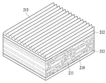
- FIG. 6 is a perspective view of a random reflective polarizer according to an exemplary embodiment of the present invention.
- FIG. 7 is a cross-sectional view of a dispersion according to a preferred embodiment of the present invention.
- FIG. 8 is a perspective view of a reflective polarizer with a lenticular pattern regularly formed according to an exemplary embodiment of the present invention
- FIG. 9 is a perspective view of a reflective polarizer with a lenticular pattern irregularly formed.
- FIG. 10 is a perspective view of a reflective polarizer with a microlens regularly formed according to an exemplary embodiment of the present invention
- FIG. 11 is a perspective view of a reflective polarizer with a microlens irregularly formed.
- FIG. 12 is a perspective view of a reflective polarizer with a prism pattern regularly formed according to an exemplary embodiment of the present invention
- FIG. 13 is a perspective view of a reflective polarizer with a prism pattern irregularly formed.
- FIG. 14 is a cross-sectional view of a coat-hanger die according to one preferred embodiment of the present invention, and FIG. 15 is a side view.
- FIG. 16 is a schematic diagram of a micropattern forming process according to an exemplary embodiment of the present invention
- FIG. 17 is a cross-sectional view illustrating a detailed structure of the molding part of FIG. 16.
- FIG. 18 is a schematic diagram of a micropattern forming process according to an exemplary embodiment of the present invention.
- FIG. 19 is a schematic diagram of a micropattern forming process according to an exemplary embodiment of the present invention.
- FIG. 20 is an exploded perspective view of a reflective polarizer in which a dispersion including the reflective polarizer of the present invention is dispersed according to another preferred embodiment of the present invention.
- the random scattering reflective polarizer of the present invention includes a plurality of dispersions inside the substrate, in order to transmit the first polarization irradiated from the outside and reflect the second polarization, the plurality of dispersions being at least one of the substrate.
- the refractive index is different in the axial direction of, wherein the aspect ratio of the short axis length to the major axis length of the plurality of dispersions contained in the substrate is longer than 1/2 based on the vertical section in the longitudinal direction, the aspect ratio is Dispersions less than 1/2 contain three or more groups of different cross-sectional area, the cross-sectional area of the first group is 0.2-2.0 ⁇ m 2 , the cross-sectional area of the second group is from 2.0 ⁇ m 2 to 5.0 ⁇ m 2 or less, and the third The cross-sectional area of the group is greater than 5.0 ⁇ m 2 to 10.0 ⁇ m 2 or less, and the dispersion of the first group, the dispersion of the second group, and the dispersion of the third group are randomly arranged core layers.
- the visible light phenomenon is improved compared to the conventional distributed reflective polarizer, and the wide viewing angle is wide and the light loss can be maximized while minimizing the light loss.
- FIG. 5 is a cross-sectional view of a reflective polarizer in which a dispersion is randomly dispersed in a substrate according to an exemplary embodiment of the present invention.
- a plurality of dispersions 201 to 206 are randomly dispersed in the substrate 200, and include core layers 200 and 201 to 206 arranged at random, and a skin layer integrally formed on at least one surface of the core layer. 207 may be further included.
- the core layer will be described.
- at least 80% of the plurality of dispersions contained in the substrate must have an aspect ratio of the short axis length to the long axis length based on the vertical cross section in the longitudinal direction of less than 1/2, more preferably at least 90%.
- Aspect ratio values should satisfy 1/2 or less.
- 7 is a vertical cross section in the longitudinal direction of a dispersion that can be used in the present invention, where the long axis length is a and the short axis length is b, the ratio of the relative lengths of the long axis length (a) and the short axis length (b) (aspect ratio) ) Should be less than 1/2.
- the short axis length (b) should be less than or equal to 1, which is 1/2. If the dispersion having a ratio of the short axis length to the long axis length of more than 1/2 is included in 20% or more of the total number of dispersions, it is difficult to achieve the desired optical properties.
- Dispersions having an aspect ratio of 1/2 or less include three or more groups of different cross-sectional areas. Specifically, in FIG. 5, dispersions 201 and 202 having the smallest cross-sectional area, dispersions 203 and 204 having a medium cross-sectional area and third groups 205 and 206 having the largest cross-sectional area. ) Are randomly dispersed, including all dispersions.
- the cross-sectional area of the first group is 0.2 to 2.0 ⁇ m 2
- the cross-sectional area of the second group is greater than 2.0 ⁇ m 2 to 5.0 ⁇ m 2 or less
- the cross-sectional area of the third group is greater than 5.0 ⁇ m 2 to 10.0 ⁇ m 2 or less
- the number of dispersions of the third group of the dispersions having an aspect ratio of 1/2 or less may be 10% or more. If less than 10%, the optical properties may be insufficient. More preferably, the number of dispersions corresponding to the first group among the dispersions having an aspect ratio of 1/2 or less may satisfy 30 to 50%, and the number of dispersions corresponding to the third group may be 10 to 30%. This can improve the optical properties (see Table 1).
- the number of dispersions of the first group / the number of dispersions of the third group has a value of 3 to 5 may be very advantageous to maximize the optical properties (see Table 1).
- the number of dispersions corresponding to the second group among the dispersions having an aspect ratio of 1/2 or less may satisfy 25 to 45%.
- the dispersion outside the range of the cross-sectional area of the first to third dispersion may be included as a residual amount in the dispersion having the aspect ratio of 1/2 or less.
- the visible light phenomenon is improved compared to the conventional distributed reflective polarizer, and the wide viewing angle is wide and the light loss is minimized while maximizing the brightness, and the wide viewing angle is wide and the light loss is minimized while maximizing the brightness enhancement.
- a skin layer 207 may be further included on at least one surface of the above-described core layer, which is integrally formed between the core layer and the skin layer 207.
- the skin layer is manufactured at the same time as the core layer and then the stretching process is performed, the skin layer of the present invention can be stretched in at least one axial direction, unlike the conventional core layer stretching, after the stretching with the unstretched skin layer. As a result, the surface hardness is improved compared to the unstretched skin layer, thereby improving scratch resistance and heat resistance.
- FIG. 6 is a perspective view of a reflective polarizer according to an exemplary embodiment of the present invention, in which a plurality of random dispersions 211 extend in a longitudinal direction of the substrate 210, such that the skin layer 212 is a core layer. It is formed at the top of the.
- the random dispersion 211 may be extended in various directions, respectively, but preferably, it is advantageously extended in parallel in one direction, and more preferably in a direction perpendicular to light irradiated from an external light source. Stretching parallel to the trunk is effective to maximize the light modulation effect.
- a birefringent interface may be formed between the dispersion (first component) and the substrate (second component) included in the substrate.
- the magnitude of the substantial coincidence or mismatch of the refractive indices along the X, Y, and Z axes in space between the substrate and the dispersion is the scattering of the polarized light along that axis. Affects the degree. In general, the scattering power varies in proportion to the square of the refractive index mismatch. Thus, the greater the degree of mismatch in refractive index along a particular axis, the more strongly scattered light polarized along that axis.
- the light polarized along that axis is scattered to a lesser extent. If the refractive index of the substrate along a certain axis substantially matches the refractive index of the dispersion, incident light polarized with an electric field parallel to this axis passes through the dispersion without scattering regardless of the size, shape and density of the portion of the dispersion. something to do. Also, when the refractive indices along that axis are substantially coincident, the light beam passes through the object without being substantially scattered.
- the first polarized light (P wave) is transmitted without being affected by the birefringent interface formed at the boundary between the substrate and the dispersion, while the second polarized light (S wave) is formed at the boundary between the substrate and the dispersion.
- the modulation of the light occurs due to the interface.
- the P wave is transmitted, and the S wave generates light modulation such as scattering and reflection of light, and thus, polarization is separated.
- the substrate and the dispersion may cause a photomodulation effect by forming a birefringent interface
- the dispersion when the substrate is optically isotropic, the dispersion may have birefringence and conversely, when the substrate is optically birefringent
- the dispersion may have optical isotropy.
- the refractive index of the dispersion is nX 1 in the x-axis direction
- the refractive index in the y-axis direction is nY 1 and the refractive index in the z-axis direction is nZ 1
- the refractive index of the substrate is nX 2 , nY 2 and nZ 2
- In-plane birefringence between nX 1 and nY 1 may occur.
- At least one of the X, Y, and Z axis refractive indices of the substrate and the dispersion may be different, and more preferably, the difference in refractive index with respect to the Y and Z axis directions is 0.05 or less when the extension axis is the X axis.
- the difference in refractive index with respect to the X-axis may be 0.1 or more. On the other hand, if the difference in refractive index is 0.05 or less, it is usually interpreted as a match.
- the thickness of the substrate in the present invention may be 20 to 180 ⁇ m, but is not limited thereto.
- the thickness of the skin layer may be 50 to 500 ⁇ m, but is not limited thereto.
- the total number of dispersions may be 25,000,000 to 80,000,000 when the thickness of the substrate is 120 ⁇ m based on 32 inches, but is not limited thereto.
- each of the dispersions may be elongated in various directions, but is preferably advantageously extended in parallel in one direction, more preferably in parallel to the elongated bodies in a direction perpendicular to the light irradiated from an external light source. Stretching is effective to maximize the light modulation effect.
- a primer layer (not shown) may be selectively formed on one surface of the skin layer 212 (one surface of the substrate when the skin layer is not included). This can improve the adhesion, appearance, and light properties of the structured surface layer. Its material may be acrylic, ester, urethane, and the like, but is not limited thereto. The primer layer may be thinner than other layers, and the thickness of the primer layer may be adjusted to improve light transmittance and to lower the reflectance.
- the thickness of this primer layer may be 5nm to 300nm. If the thickness of the primer layer is less than 5 nm, the adhesion between the core layer and the structured surface layer may be insignificant. If the thickness of the primer layer exceeds 300 nm, staining or agglomeration of molecules may occur during the primer treatment.
- the reflective polarizer of the present invention can form a structured surface layer on at least one surface to maximize the condensing effect and prevent diffuse reflection on the surface to significantly improve the brightness.
- the structured surface layer can be formed on a substrate or on a primer layer.
- the structured surface layer that can be applied in the present invention is preferably a fine pattern layer as a structure capable of improving the light collecting effect.
- the micropattern that can be applied may be any one or more selected from the group consisting of prisms, lenticulars, microlenses, triangular pyramids, and pyramid patterns, each of which may be formed by combining or forming a pattern alone.
- the skin layer 212 and the lenticular pattern layer 213 are formed on one surface of the base layer of the reflective polarizer.
- the height a of the lenticular may be 10 to 50 ⁇ m. If the height of the lenticular pattern is less than 10 ⁇ m, it may be difficult to implement the pattern layer. If the height of the lenticular pattern exceeds 50 ⁇ m, the luminance may decrease due to an increase in total reflection of light.
- the pitch b of the lenticular may be 20 to 100 ⁇ m. If the pitch of the lenticular pattern is less than 20 ⁇ m, the condensing effect of the lens shape is somewhat decreased due to the increase of the valley portion of the film per unit area, and the limitation of the precision of the shape processing and the pattern shape are too narrow may cause a problem of difficult to implement the pattern. If the thickness exceeds 100 ⁇ m, the possibility of moiré between the pattern structure and the panel becomes very large.
- the ratio of the major axis / short axis b / a satisfies 1.0 to 3.0.
- the ratio of the long axis / short axis (b / a) is out of the above range, there may occur a problem that the linear concealment efficiency with respect to light passing through the birefringent polarization layer is inferior.
- the tangential angle ⁇ at both ends of the lower end of the lens must satisfy 30 to 80 degrees. At this time, when ⁇ is smaller than 30 degrees, the concealment efficiency of the bright line is inferior, and when ⁇ is larger than 80 degrees, there is a problem that the production of the lens pattern becomes difficult. If the cross-sectional shape of the lenticular lens is a triangle, it is preferable that the vertex angle ⁇ satisfies 90 to 120 degrees for the concealed light effect.
- the lenticular shape may be formed in a pattern having the same height and pitch as shown in FIG. 8, or lenticular patterns having different heights and pitches may be mixed as shown in FIG. 9.
- FIG. 10 illustrates that a microlens pattern layer is formed on one surface of a reflective polarizer.
- the height of the microlens may be 10 to 50 ⁇ m. If the height of the micro-lens pattern is less than 10 ⁇ m may cause a problem of light condensing slightly and difficult to implement the pattern, if it exceeds 50 ⁇ m may cause a moire phenomenon, a problem that the pattern is visible on the image.
- the diameter of the micro lens may be 20 ⁇ 100 ⁇ m. Preferably it may be 30 ⁇ 60 ⁇ m. While the appearance characteristics are good in the above range, the light condensing function and the light diffusing characteristics of the microlenses may be excellent and the actual manufacturing may be easy. If the diameter of the microlens pattern is less than 20 ⁇ m, a problem may occur that shows a low light collection efficiency for incident light incident from an invalid angle. If the diameter of the micro lens pattern exceeds 100 ⁇ m, the light collection efficiency for vertical light may be deteriorated. May occur.
- the microlens pattern layer may also be formed in a pattern having the same height and diameter as shown in FIG. 10, or microlens patterns having different heights and diameters may be mixed as shown in FIG. 11. Since the microlens pattern has a large difference in optical characteristics according to the density of the lens and the degree of impregnation, the microlens pattern may have the highest density, and the degree of impregnation should be 1/2.
- the prism pattern layer 213 is formed on one surface of the reflective polarizer, and the prism height a may be about 10 ⁇ m to about 50 ⁇ m. If the height of the prism pattern is less than 10 ⁇ m, the base film may be damaged by pressure when manufacturing the shape of the prism pattern part. If the height of the prism pattern exceeds 50 ⁇ m, the transmittance of light incident on the light source may be reduced.
- the pitch b of the prism may be 20 to 100 ⁇ m. If the pitch of the prism pattern is less than 20 ⁇ m, the engraving is not good, and the pattern layer implementation and manufacturing process may have complicated problems. If it exceeds 100 ⁇ m, the moire phenomenon is likely to occur, and the pattern may be seen on the image. .
- the prism shape may be formed in a pattern having the same height and pitch as shown in FIG. 12, or the prism patterns having different heights and pitches as shown in FIG. 13 may be mixed.
- the prism pattern may be formed of a material having a higher refractive index than that of the base film. When the refractive index of the base film is higher, a part of the light incident to the rear surface of the base film may be totally reflected at the surface of the prism pattern and thus may not be incident to the prism structure. Because.
- the prism shape is a linear prism shape, the vertical cross section is triangular, and the triangle forms an angle of 60 to 110 ° with a vertex facing the lower surface.
- the material of the structured surface layer may preferably be a polymer resin including a thermosetting or photocurable acrylic resin or the like.
- a polymer resin including a thermosetting or photocurable acrylic resin or the like For example, as the prism pattern, unsaturated fatty acid esters, aromatic vinyl compounds, unsaturated fatty acids and derivatives thereof, vinyl cyanide compounds such as methacrylonitrile, and the like may be used. Specifically, urethane acrylates and methacryl acrylates may be used. Resins and the like can be used.
- the structured surface layer may also be made of a material having a higher refractive index than the reflective polarizer.
- the base component, the dispersion component, and the skin layer component are supplied to the extrusion unit.
- the substrate component may be used without limitation as long as it is used in a reflective polarizer in which a conventional dispersion is dispersed.
- polyethylene naphthalate PEN
- copolyethylene naphthalate co-PEN
- polyethylene terephthalate PET
- PC poly Carbonate
- PC polycarbonate
- PS polystyrene
- PS heat-resistant polystyrene
- PMMA polymethyl methacrylate
- PBT polybutylene terephthalate
- PP polypropylene
- PE polyethylene
- PE acrylonitrile butadiene styrene
- ABS polyurethane
- PU polyimide
- PVC polyvinyl chloride
- SAN ethylene vinyl acetate
- EVA ethylene vinyl acetate
- PA polyamide
- POM polyacetal
- phenol epoxy
- EP urea
- UF melanin
- MF unsaturated polyesters
- UP unsaturated polyesters
- SI silicone
- cycloolefin polymers may be used and more preferably May be PEN.
- the dispersion component may be used without limitation as long as the dispersion component is used in a reflective polarizer in which the dispersion is dispersed.
- PEN polyethylene naphthalate
- PET polyethylene terephthalate
- PC Polycarbonate
- PC Polycarbonate
- PC Polycarbonate
- PC Polycarbonate
- Alloy Polystyrene (PS), Heat Resistant Polystyrene (PS), Polymethylmethacrylate (PMMA), Polybutylene Terephthalate (PBT), Polypropylene (PP), Polyethylene (PE), acrylonitrile butadiene styrene (ABS), polyurethane (PU), polyimide (PI), polyvinyl chloride (PVC), styrene acrylonitrile mixture (SAN), ethylene vinyl acetate (EVA), poly Amide (PA), polyacetal (POM), phenol, epoxy (EP), urea (UF), melanin (MF), unsaturated polyester (UP),
- PA
- the skin layer component may be used a component that is commonly used but preferably may be used without limitation as long as it is used in the reflective polarizer, preferably polyethylene naphthalate (PEN), copolyethylene naphthalate (co-PEN), polyethylene Terephthalate (PET), Polycarbonate (PC), Polycarbonate (PC) Alloy, Polystyrene (PS), Heat-Resistant Polystyrene (PS), Polymethylmethacrylate (PMMA), Polybutylene Terephthalate (PBT), Poly Propylene (PP), Polyethylene (PE), Acrylonitrile Butadiene Styrene (ABS), Polyurethane (PU), Polyimide (PI), Polyvinyl Chloride (PVC), Styrene Acrylonitrile Mixture (SAN), Ethylene Acetic Acid Vinyl (EVA), polyamide (PA), polyacetal (POM), phenol, epoxy (EP), urea (UF), melanin (MF), unsaturated polyester (UP), silicone (SI
- the base component and the dispersion component may be supplied to the independent extrusion parts separately, in this case, the extrusion part may be composed of two or more.
- a feed to one extruder comprising a separate feed passage and distributor so that the polymers do not mix.
- the extruder may be an extruder, which may further include heating means or the like to convert the supplied polymers into a liquid phase.
- the viscosity is so designed that there is a difference in polymer flow so that the dispersion component can be arranged inside the base component, and the base component is preferably made to have better flowability than the dispersion component.
- the dispersion component is randomly arranged in the substrate through the difference in viscosity while the substrate component and the dispersion component pass through the mixing zone and the mesh filter zone.
- the prepared core layer may be laminated with the skin layer component transferred from the extruder.
- the skin layer component may be laminated on both surfaces of the core layer.
- the material and the thickness of the skin layer may be the same or different from each other.
- FIG. 14 is a cross-sectional view of a coat-hanger die which is a kind of preferred flow control unit that can be applied to the present invention
- FIG. 15 is a side view.
- the spreading degree of the substrate may be appropriately adjusted to randomly adjust the size and arrangement of the cross-sectional area of the dispersion component.
- the dispersion component contained therein also spreads from side to side.
- the cooling used in the manufacture of the conventional reflective polarizer is solidified, and then the smoothing step may be performed through a casting roll process or the like.
- the stretching may be performed through a stretching process of a conventional reflective polarizer, thereby causing a difference in refractive index between the base component and the dispersion component, causing a light modulation phenomenon at the interface, and spreading the first component (dispersion).
- Sieve components the aspect ratio is further reduced through stretching.
- the stretching step may be performed uniaxially or biaxially, and more preferably, uniaxially.
- the stretching direction may be performed in the longitudinal direction of the first component.
- the draw ratio may be 3 to 12 times.
- methods for changing an isotropic material to birefringence are commonly known and, for example, when drawn under appropriate temperature conditions, the dispersion molecules can be oriented so that the material becomes birefringent.
- the final reflective polarizer may be manufactured by heat setting the stretched polarizer.
- the heat setting may be heat setting through a conventional method, preferably may be performed through an IR heater for 0.1 to 3 minutes at 180 ⁇ 200 °C.
- a structured surface layer is formed on at least one surface of the reflective polarizer (core layer or skin layer) manufactured as step (2).
- a primer layer may be further formed on at least one surface of the core layer (or skin layer). This can improve the adhesion, appearance, and light properties of the structured surface layer.
- Its material may be acrylic, ester, urethane, and the like, but is not limited thereto.
- the primer layer may be thinner than other layers, and the thickness of the primer layer may be adjusted to improve light transmittance and to lower the reflectance.
- the thickness of this primer layer may be 5nm to 300nm. If the thickness of the primer layer is less than 5 nm, the adhesion between the core layer and the structured surface layer may be insignificant. If the thickness of the primer layer exceeds 300 nm, staining or agglomeration of molecules may occur during the primer treatment.
- the reflective polarizer of the present invention can form a structured surface layer on at least one surface to maximize the condensing effect and prevent diffuse reflection on the surface to significantly improve the brightness.
- the structured surface layer that can be applied in the present invention is preferably a fine pattern layer as a structure capable of improving the light collecting effect.
- the micropattern that can be applied may be any one or more selected from the group consisting of prisms, lenticulars, microlenses, triangular pyramids, and pyramid patterns, each of which may be formed by combining or forming a pattern alone.
- the pattern may be arranged in a constant or different height, pitch, and the like.
- the material of the structured surface layer may preferably be a polymer resin including a thermosetting or photocurable acrylic resin or the like.
- the prism pattern may be unsaturated fatty acid esters, aromatic vinyl compounds, unsaturated fatty acids and derivatives thereof, vinyl cyanide compounds such as methacrylonitrile, and the like, and specifically, urethane acrylate and methacrylic acrylic Rate resins and the like can be used.
- the structured surface layer may also be made of a material having a higher refractive index than the reflective polarizer.
- the fine pattern layer may be manufactured through a mold film for pattern formation.
- a material of the mold film for pattern formation a film having a transparent, flexible, predetermined tensile strength and durability may be used, and it is preferable to use a PET film.
- the step (2) is 2-1) to transfer the reflective polarizer in close contact with the master roll formed on one surface of the reversed pattern of the structured surface layer, Applying a molten polymer resin to a pattern surface or the core layer surface; And 2-2) UV curing and separating the polymer resin by UV or heat while the polymer resin is press-molded on the patterned surface of the master roll.
- step 2-2 after the step 2-2) may be irradiated with UV or heat again to cure the polymer resin secondary.
- FIG. 16 is a schematic diagram of a micropattern forming process according to an exemplary embodiment of the present invention
- FIG. 17 is a cross-sectional view illustrating a detailed structure of the molding part of FIG. 16.
- the reflective polarizer 770 passes through the infrared lamp 751 through the guide roll 754 while being released from the start trol 755.
- the reflective polarizer 770 is surface-modified by the infrared rays of the infrared lamp, so that the adhesion to the pattern forming layer 771 is improved.
- the pattern forming layer is formed on the pattern surface of the master roll 705 from the injection portion 742.
- a material and a pattern layer polymer are coated to merge with the base layer 770.
- the resin is a resin melted at room temperature, and may be primarily cured due to the primary UV light irradiated from the primary UV curing device 752 disposed under the master roll 705.
- the temperature around the curing apparatus 752 is 20 ⁇ 30 °C
- the temperature of heat generated while the resin is cured is 40 ⁇ 80 °C as the glass transition temperature (Tg: polymer resin) of the resin
- the pattern forming layer 771 completely copying the pattern of the surface of the master roll exits through the pattern guide roll 764 and forms a pattern in which the reflective polarizer 770 and the pattern forming layer 771 are combined. It is molded into a reflective polarizer 772 and wound around the guide roll 754 to the finish roll 756.
- the cross-section of the turn-shaped reflective polarizer 772 formed by irradiating UV over two times is a surface opposite to the cross-section of the master roll 705. If it is an engraved surface, the turn-shaped reflective polarizer 772 becomes an embossed surface of the relief.
- step (2) comprises the steps of: a) transferring the reflective polarizer; b) transferring the pattern forming mold film formed on one surface of the reversed pattern of the structured surface layer; c) contacting one surface of the reflective polarizer with one surface of the patterned mold film; d) filling the pattern by injecting a fluid material into an area where the reflective polarizer and the pattern forming mold film are in close contact; e) applying the material to the reflective polarizer by curing the material filled between the patterns; And f) separating the pattern forming mold film and the reflective polarizer coated with the material, and the steps a) and b) may be performed regardless of the order.
- the method may further include filling the material evenly between the patterns by applying pressure to the reflective polarizer and the mold film in close contact between the steps d) and e).
- step e) may comprise irradiating heat or UV to the material filled between the patterns.
- Figure 18 is a schematic diagram of a micropattern forming process according to another preferred embodiment of the present invention.
- the reflective polarizer 810 wound on the first roll 820 is transferred by the guide rolls 830a to 830c.
- the molding mold 842 of the pattern molding part 840 is also in a state of being transferred / rotated while being wound around the master roll 844 and the pattern guide rolls 846a and 846b.
- the reflective polarizer 810 is drawn by the guide roll 830c to be engaged with the molding mold 842.
- the guide roll 830c performs a gap adjustment function for adjusting the thickness of the coating layer applied to the reflective polarizer 810, that is, the pattern layer of the reflective polarizer 812 having the resin layer patterned therein. More specifically, when the guide roll 830c is in close contact with the master roll 844, the pattern layer of the reflective polarizer may be formed thinner. On the contrary, when the guide roll 830c is further apart from the master roll, the reflective polarizer may be formed. The pattern layer can be formed thicker. The thickness of such a reflective polarizer pattern layer can be adjusted by the viscosity of the coating liquid, the patterning speed, the tension of the reflective polarizer, and the like, in addition to the gap between the guide roll 830c and the master roll 844.
- the reflective polarizer 810 is filled with the coating liquid is injected by the coating liquid injection means 860 to the point where the guide roll 830c and the master roll 844 is engaged, and is pushed and filled between the pattern of the molding mold 842,
- the pressure is uniformly distributed and patterned by the pressure between the guide roll 830c and the master roll 844.
- the coating liquid distributed between the patterns is cured by heat or UV emitted from the curing means 870.
- the reflective polarizer in which the patterned coating solution is cured and applied is separated from the molding mold 842 while being drawn by the guide roll 830d, and the reflective polarizer 812 having the pattern formed is transferred by the guide roll 830e. It is wound on two rolls 850.
- the guide roll 830d performs a peeling function to separate the reflective polarizer 812 to which the coating liquid is applied, that is, the pattern layer is formed from the molding mold 842.
- the reflective polarizer 810 and the reflective polarizer 812 on which the pattern layer is formed are classified for convenience of description in a state of being connected to each other. That is, the reflective polarizer 810 refers to a state before the pattern is formed, and the reflective polarizer 812 having the pattern layer passes through the pattern molding part 840 while the patterned coating liquid is applied to the reflective polarizer. It means completed state. 18 illustrates only a part of the pattern layer formed on the reflective polarizer 812 on which the pattern layer is formed, and in reality, the reflective polarizer wound on the second roll 850 is also in a state where the pattern layer is formed.
- FIG. 19 is a schematic diagram of a micropattern forming process according to another preferred embodiment of the present invention.
- the forming mold 942 is formed in a roll type as long as the length of the reflective polarizer 910 so that the reflective polarizer 912 having the patterned layer is seamlessly formed.
- the first roll 920 on which the reflective polarizer 910 is wound and the second roll 950 on which the reflective polarizer 912 having the pattern layer are wound are wound.
- Guide rolls 930a to 930f provided on both sides and transferring the reflective polarizer and the reflective polarizer having the patterned layer are provided between the first roll 920 and the second roll 950.
- the master roll 946 of the pattern molding part 940 is in close contact between the guide roll 930c and the guide roll 930d to apply a patterned coating solution to the reflective polarizer 910.
- the number and position of the guide rolls 930a to 930f may be changed depending on the embodiment.
- the pattern molding part 940 compresses the coating liquid according to the pattern of the molding mold by compressing a molding mold 942 having a film shape with a pattern shape, a third roll 944 on which the molding mold is wound, and a coating liquid injected into the molding mold. It consists of a master roll 946 for shaping and applying it to the reflective polarizer 910, pattern guide rolls 947a to 947d for conveying the molding mold, and a fourth roll 948 to which the transferred molding mold is wound. The number and position of the pattern guide rolls 947a to 947d can be changed depending on the embodiment.
- the forming mold 942 is wound on the third roll 944 and is conveyed by the master roll 946 and the guide rolls 947a to 947d to the reflective polarizer 910.
- the molding mold 942 is preferably formed to have the same length as the reflective polarizer 910, through which the entire pattern of the reflective polarizer 912 having the pattern layer without defects or pattern breakage due to the seam. The pattern is formed evenly over.
- FIG. 19 only a part of the pattern embodied in the pattern layer of the molding mold is illustrated, but in practice, the pattern is implemented throughout the molding mold.
- a coating liquid injection means 960 for injecting a coating liquid is provided.
- curing means 970 is provided to cure the coating liquid by irradiating heat or UV.
- FIG. 20 is an example of a liquid crystal display device employing a reflective polarizer of the present invention, in which a reflecting plate 280 is inserted into a frame 270, and a cold cathode fluorescent lamp 290 is disposed on an upper surface of the reflecting plate 280. Is located.
- An optical film 320 is positioned on an upper surface of the cold cathode fluorescent lamp 290, and the optical film 320 includes a diffuser plate 321, a light diffusion film 322, a prism film 323, and a reflective polarizer ( 324 and the absorption polarizing film 325 are laminated in this order, but the stacking order may vary depending on the purpose or some components may be omitted or a plurality may be provided.
- the diffusion plate 321, the light diffusing film 322, the prism film 323, and the like may be excluded from the overall configuration, and may be changed in order or formed at different positions.
- a retardation film (not shown) or the like may also be inserted at an appropriate position in the liquid crystal display device.
- the liquid crystal display panel 310 may be inserted into the mold frame 300 on the upper surface of the optical film 320.
- the light irradiated from the cold cathode fluorescent lamp 290 reaches the diffusion plate 321 of the optical film 320.
- the light transmitted through the diffusion plate 321 passes through the light diffusion film 322 in order to propagate the light in the vertical direction with respect to the optical film 320.
- the film passing through the light diffusion film 322 passes through the prism film 323 and reaches the reflective polarizer 324 to generate light modulation.
- the P wave transmits the reflective polarizer 324 without loss, but in the case of the S wave, light modulation (reflection, scattering, refraction, etc.) is generated, and again, by the reflecting plate 280 that is the rear side of the cold cathode fluorescent lamp 290.
- the reflective polarizer of the present invention when used by being inserted into the liquid crystal display device, a dramatic improvement in luminance can be expected as compared with a conventional reflective polarizer. Meanwhile, the cold cathode fluorescent lamp 290 may be replaced with an LED.
- the use of the reflective polarizer has been described based on the liquid crystal display, but the present invention is not limited thereto, and may be widely used in flat panel display technologies such as a projection display, a plasma display, a field emission display, and an electroluminescent display.
- PCTG polycyclohexylene dimethylene terephthalate
- thermal stabilizer containing phosphate The raw material was put into the 1st extrusion part and the 2nd extrusion part, respectively.
- PCTG polycyclohexylene dimethylene terephthalate
- the extrusion temperature of the base component and the dispersion component is set to 245 ° C. and confirmed by Cap.Rheometer.
- Cap.Rheometer Cap.Rheometer
- the polymer flow was corrected, and the dispersion was randomly dispersed in the substrate by passing through the flow path to which the filter mixer was applied, and then the skin layer component was laminated on both sides of the substrate layer component.
- the polymer was induced to spread in the coat hanger dies of FIGS. 14 and 15 to correct flow rates and pressure gradients.
- the width of the die inlet is 200 mm
- the thickness is 10 mm
- the width of the die outlet is 1260 mm
- the thickness is 2.5 mm
- the flow rate is 1.0 m / min.
- a smoothing process was then performed on the cooling and casting rolls and stretched six times in the MD direction. Subsequently, heat setting was performed through a heater chamber at 180 ° C. for 2 minutes to prepare a randomly distributed polarizer as shown in Table 1 having a thickness of 120 ⁇ m (300 ⁇ m including a skin layer).
- the refractive index of the polyetherene naphthalate (PEN) component of the prepared reflective polarizer was (nx: 1.88, ny: 1.58, nz: 1.58) and terephthalate, ethyl glycol, and cyclohexanedimethanol 1: 60 wt% polycarbonate.
- the refractive index of 38 wt% of polycyclohexylene dimethylene terephthalate (PCTG) polymerized at 2 molar ratio and 2 wt% of the thermal stabilizer containing phosphate was 1.58.
- Core layer thickness is 120 micrometers
- skin layer thickness is 90 micrometers, respectively.
- the prepared reflective polarizer was manufactured in the same manner as in FIG. 19 to form a reflective polarizer having a urethane acrylic prism pattern layer having a refractive index of 1.59.
- the height was 20 mu m and the pitch was 40 mu m.
- the luminance of the prepared reflective polarizer was performed as follows. After assembling the panel on a 32 "direct backlight unit equipped with a diffuser plate and a reflective polarizer, the luminance was measured at nine points using a BM-7 measuring instrument manufactured by Topcon Corporation.
- the relative luminance shows the relative values of the luminance of the other examples and comparative examples when the luminance of the reflective polarizer of Example 1 is 100 (reference).
- Reflective polarizer diffuser plate, diffusion sheet, prism sheet, brightness enhancement film
- the linearity evaluation was performed by visually observing the linear curves and evaluating the number of linear curves as 0, very good, 1 good, 2 or 3 normal, and 4 or 5 poor.
- the aspect ratio represents the number of dispersions having an aspect ratio of 1/2 or less, as a percentage of the total dispersions
- Group 1, Group 2, and Group 3 represent the number of dispersions in the cross-sectional area range of Groups 1, 2, and 3 of the present invention in% among the dispersions having an aspect ratio of 1/2 or less,
- the 1/3 group represents the number of 1 group / 3 groups in%.
- Examples 1 to 5 satisfying the scope of the present invention was superior in brightness, polarization degree and linearity compared to Comparative Examples 1 and 2, which do not satisfy this.
- Example 1 belonging to the range of 1/3 group of the present invention showed excellent optical properties compared to Examples 2 to 4 that do not satisfy this.
- the optical properties of Example 1 were very excellent compared to Example 5, where the content of Group 1 was out of range.
- the reflective polarizer of the present invention Since the reflective polarizer of the present invention has excellent light modulation performance, it can be widely used in a field requiring modulation of light. Specifically, it can be widely used in flat panel display technologies such as liquid crystal displays, projection displays, plasma displays, field emission displays, and electroluminescent displays that require high brightness such as mobile displays, LCDs, and LEDs.
Landscapes
- Physics & Mathematics (AREA)
- General Physics & Mathematics (AREA)
- Optics & Photonics (AREA)
- Engineering & Computer Science (AREA)
- Nonlinear Science (AREA)
- Chemical & Material Sciences (AREA)
- Crystallography & Structural Chemistry (AREA)
- Health & Medical Sciences (AREA)
- Mechanical Engineering (AREA)
- Ophthalmology & Optometry (AREA)
- Manufacturing & Machinery (AREA)
- Mathematical Physics (AREA)
- Polarising Elements (AREA)
Abstract
Priority Applications (4)
| Application Number | Priority Date | Filing Date | Title |
|---|---|---|---|
| JP2016561984A JP6218970B2 (ja) | 2013-12-31 | 2014-12-30 | ランダム分散型反射偏光子 |
| CN201480071240.9A CN105874362B (zh) | 2013-12-31 | 2014-12-30 | 随机散布式反射偏光器 |
| US15/107,752 US9952363B2 (en) | 2013-12-31 | 2014-12-30 | Random dispersion-type reflection polarizer |
| EP14877113.2A EP3091378B1 (fr) | 2013-12-31 | 2014-12-30 | Polariseur réfléchissant de type à dispersion aléatoire |
Applications Claiming Priority (4)
| Application Number | Priority Date | Filing Date | Title |
|---|---|---|---|
| KR1020130169217A KR102172288B1 (ko) | 2013-12-31 | 2013-12-31 | 랜덤 분산형 반사 편광자 |
| KR10-2013-0169215 | 2013-12-31 | ||
| KR1020130169215A KR102172539B1 (ko) | 2013-12-31 | 2013-12-31 | 랜덤 분산형 반사 편광자 |
| KR10-2013-0169217 | 2013-12-31 |
Publications (1)
| Publication Number | Publication Date |
|---|---|
| WO2015102364A1 true WO2015102364A1 (fr) | 2015-07-09 |
Family
ID=53493647
Family Applications (1)
| Application Number | Title | Priority Date | Filing Date |
|---|---|---|---|
| PCT/KR2014/013030 Ceased WO2015102364A1 (fr) | 2013-12-31 | 2014-12-30 | Polariseur réfléchissant de type à dispersion aléatoire |
Country Status (5)
| Country | Link |
|---|---|
| US (1) | US9952363B2 (fr) |
| EP (1) | EP3091378B1 (fr) |
| JP (1) | JP6218970B2 (fr) |
| CN (1) | CN105874362B (fr) |
| WO (1) | WO2015102364A1 (fr) |
Cited By (1)
| Publication number | Priority date | Publication date | Assignee | Title |
|---|---|---|---|---|
| JP2018509653A (ja) * | 2015-02-27 | 2018-04-05 | スリーエム イノベイティブ プロパティズ カンパニー | コリメート反射偏光子及び構造化層を含む光学フィルム |
Families Citing this family (6)
| Publication number | Priority date | Publication date | Assignee | Title |
|---|---|---|---|---|
| KR102309921B1 (ko) * | 2015-03-16 | 2021-10-07 | 삼성디스플레이 주식회사 | 표시 장치 및 이에 포함되는 광학 필름 |
| KR102367295B1 (ko) * | 2015-06-26 | 2022-02-23 | 도레이첨단소재 주식회사 | 반사편광자 및 이를 포함하는 백라이트 유닛 |
| KR101915110B1 (ko) * | 2015-12-29 | 2018-11-05 | 도레이케미칼 주식회사 | 복합 반사편광 필름의 제조방법 |
| KR102562045B1 (ko) * | 2016-08-31 | 2023-08-01 | 엘지디스플레이 주식회사 | 확산 시트 및 이를 갖는 디스플레이 장치 |
| USD999068S1 (en) * | 2022-02-27 | 2023-09-19 | Cartier International Ag | Wrist watch |
| EP4537138A1 (fr) * | 2022-06-08 | 2025-04-16 | 3M Innovative Properties Company | Film optiquement diffusif et système optique le comprenant |
Citations (5)
| Publication number | Priority date | Publication date | Assignee | Title |
|---|---|---|---|---|
| KR20020077399A (ko) * | 2000-01-27 | 2002-10-11 | 후지 샤신 필름 가부시기가이샤 | 광산란형 편광소자 및 광흡수형 편광소자가 적층된 편광판 |
| KR20030001295A (ko) * | 2001-06-22 | 2003-01-06 | 다이셀 가가꾸 고교 가부시끼가이샤 | 편광소자, 및 이를 이용한 면광원 장치 및 액정 표시 장치 |
| KR20080056687A (ko) * | 2006-12-18 | 2008-06-23 | 롬 앤드 하스 덴마크 파이낸스 에이에스 | 폴리머 도메인을 가진 형상 아티클 및 프로세스 |
| JP2009282211A (ja) * | 2008-05-21 | 2009-12-03 | Hitachi Maxell Ltd | 反射偏光子、それを用いたバックライト及び液晶表示装置 |
| WO2013100661A1 (fr) * | 2011-12-29 | 2013-07-04 | 웅진케미칼 주식회사 | Polariseur réfléchissant comprenant un polymère dispersé |
Family Cites Families (16)
| Publication number | Priority date | Publication date | Assignee | Title |
|---|---|---|---|---|
| BR9707766A (pt) * | 1996-02-29 | 1999-07-27 | Minnesota Mining & Mfg | Corpo ótico |
| US5867316A (en) * | 1996-02-29 | 1999-02-02 | Minnesota Mining And Manufacturing Company | Multilayer film having a continuous and disperse phase |
| US5825543A (en) * | 1996-02-29 | 1998-10-20 | Minnesota Mining And Manufacturing Company | Diffusely reflecting polarizing element including a first birefringent phase and a second phase |
| US5783120A (en) * | 1996-02-29 | 1998-07-21 | Minnesota Mining And Manufacturing Company | Method for making an optical film |
| DE69721505T2 (de) * | 1996-02-29 | 2003-11-20 | Minnesota Mining And Manufacturing Company, St. Paul | Film zur helligkeitserhoehung |
| US6256146B1 (en) * | 1998-07-31 | 2001-07-03 | 3M Innovative Properties | Post-forming continuous/disperse phase optical bodies |
| US6005713A (en) * | 1998-08-21 | 1999-12-21 | 3M Innovative Properties Company | Multilayer polarizer having a continuous and disperse phase |
| JP4253472B2 (ja) * | 2001-06-22 | 2009-04-15 | ダイセル化学工業株式会社 | 偏光素子並びにそれを用いた面光源装置及び液晶表示装置 |
| CN101176018A (zh) * | 2005-04-06 | 2008-05-07 | 3M创新有限公司 | 含有可取向的聚合物共混物的漫反射偏振膜 |
| EP1890869B1 (fr) * | 2005-04-06 | 2008-10-15 | 3M Innovative Properties Company | Corps optiques contenant des couches limites pelables rugueuses et des structures asymetriques en surface |
| US20060227421A1 (en) * | 2005-04-06 | 2006-10-12 | Stover Carl A | Optical bodies including strippable boundary layers |
| KR100957496B1 (ko) * | 2007-11-26 | 2010-05-14 | 엘지전자 주식회사 | 반사형 편광 필름, 이를 포함하는 백라이트 유닛 및액정표시장치 |
| JP2009128904A (ja) * | 2007-11-26 | 2009-06-11 | Lg Electronics Inc | 光学フィルム及び液晶表示装置 |
| KR101703363B1 (ko) * | 2008-11-19 | 2017-02-06 | 쓰리엠 이노베이티브 프로퍼티즈 컴파니 | 조명 기구 및 다른 조명 시스템에서의 광 관리를 위한 브루스터 각 필름 |
| JP6251569B2 (ja) * | 2010-06-30 | 2018-01-10 | スリーエム イノベイティブ プロパティズ カンパニー | 空間的に選択的な複屈折性の減少を有する拡散反射光学フィルム |
| CN103460091B (zh) * | 2011-02-09 | 2016-05-11 | 熊津化学有限公司 | 聚合物分散的反射式偏光器 |
-
2014
- 2014-12-30 WO PCT/KR2014/013030 patent/WO2015102364A1/fr not_active Ceased
- 2014-12-30 CN CN201480071240.9A patent/CN105874362B/zh active Active
- 2014-12-30 US US15/107,752 patent/US9952363B2/en active Active
- 2014-12-30 JP JP2016561984A patent/JP6218970B2/ja active Active
- 2014-12-30 EP EP14877113.2A patent/EP3091378B1/fr active Active
Patent Citations (5)
| Publication number | Priority date | Publication date | Assignee | Title |
|---|---|---|---|---|
| KR20020077399A (ko) * | 2000-01-27 | 2002-10-11 | 후지 샤신 필름 가부시기가이샤 | 광산란형 편광소자 및 광흡수형 편광소자가 적층된 편광판 |
| KR20030001295A (ko) * | 2001-06-22 | 2003-01-06 | 다이셀 가가꾸 고교 가부시끼가이샤 | 편광소자, 및 이를 이용한 면광원 장치 및 액정 표시 장치 |
| KR20080056687A (ko) * | 2006-12-18 | 2008-06-23 | 롬 앤드 하스 덴마크 파이낸스 에이에스 | 폴리머 도메인을 가진 형상 아티클 및 프로세스 |
| JP2009282211A (ja) * | 2008-05-21 | 2009-12-03 | Hitachi Maxell Ltd | 反射偏光子、それを用いたバックライト及び液晶表示装置 |
| WO2013100661A1 (fr) * | 2011-12-29 | 2013-07-04 | 웅진케미칼 주식회사 | Polariseur réfléchissant comprenant un polymère dispersé |
Cited By (1)
| Publication number | Priority date | Publication date | Assignee | Title |
|---|---|---|---|---|
| JP2018509653A (ja) * | 2015-02-27 | 2018-04-05 | スリーエム イノベイティブ プロパティズ カンパニー | コリメート反射偏光子及び構造化層を含む光学フィルム |
Also Published As
| Publication number | Publication date |
|---|---|
| JP2017501458A (ja) | 2017-01-12 |
| CN105874362B (zh) | 2018-08-03 |
| JP6218970B2 (ja) | 2017-10-25 |
| EP3091378B1 (fr) | 2019-02-27 |
| EP3091378A1 (fr) | 2016-11-09 |
| EP3091378A4 (fr) | 2017-08-16 |
| CN105874362A (zh) | 2016-08-17 |
| US9952363B2 (en) | 2018-04-24 |
| US20160320537A1 (en) | 2016-11-03 |
Similar Documents
| Publication | Publication Date | Title |
|---|---|---|
| KR102172539B1 (ko) | 랜덤 분산형 반사 편광자 | |
| WO2015102364A1 (fr) | Polariseur réfléchissant de type à dispersion aléatoire | |
| TWI606284B (zh) | 隨機散布式反射偏光器 | |
| WO2012108674A2 (fr) | Procédé et appareil pour fabriquer un polariseur réfléchissant ayant un polymère dispersé | |
| US12111532B2 (en) | Optical body and display device including same | |
| WO2023058954A1 (fr) | Film polarisant réfléchissant, et ensemble source de lumière et dispositif d'affichage liquide comprenant chacun celui-ci | |
| KR102172288B1 (ko) | 랜덤 분산형 반사 편광자 | |
| KR102698488B1 (ko) | 광학체 및 이를 포함하는 표시장치 | |
| WO2013100662A1 (fr) | Procédé et appareil de fabrication d'un polariseur réfléchissant comprenant un polymère dispersé | |
| KR102698461B1 (ko) | 광학체 및 이를 포함하는 표시장치 | |
| WO2013100661A1 (fr) | Polariseur réfléchissant comprenant un polymère dispersé | |
| KR102540191B1 (ko) | 광학체 및 이를 포함하는 표시장치 | |
| KR101906251B1 (ko) | 다층 반사편광자 및 그 제조방법 | |
| KR101685574B1 (ko) | 복합 반사편광 필름 | |
| KR101701500B1 (ko) | 복합 반사편광 필름 | |
| KR101906253B1 (ko) | 폴리머가 분산된 반사 편광자 및 그 제조방법 | |
| KR102698463B1 (ko) | 광학체 및 이를 포함하는 표시장치 | |
| WO2013100663A1 (fr) | Polariseur réfléchissant multicouche | |
| KR101906252B1 (ko) | 다층 반사편광자 및 그 제조방법 | |
| KR102551104B1 (ko) | 반사편광필름 및 이를 포함하는 표시장치 | |
| KR101685586B1 (ko) | 복합 반사편광 필름 | |
| KR101714388B1 (ko) | 반사편광 필름 및 그 제조방법 | |
| KR101685588B1 (ko) | 복합 반사편광 필름 | |
| WO2013100664A1 (fr) | Procédé et appareil de fabrication d'un polariseur réfléchissant multicouche | |
| KR20200060079A (ko) | 광학체 및 이를 포함하는 표시장치 |
Legal Events
| Date | Code | Title | Description |
|---|---|---|---|
| 121 | Ep: the epo has been informed by wipo that ep was designated in this application |
Ref document number: 14877113 Country of ref document: EP Kind code of ref document: A1 |
|
| WWE | Wipo information: entry into national phase |
Ref document number: 15107752 Country of ref document: US |
|
| ENP | Entry into the national phase |
Ref document number: 2016561984 Country of ref document: JP Kind code of ref document: A |
|
| NENP | Non-entry into the national phase |
Ref country code: DE |
|
| REEP | Request for entry into the european phase |
Ref document number: 2014877113 Country of ref document: EP |
|
| WWE | Wipo information: entry into national phase |
Ref document number: 2014877113 Country of ref document: EP |