WO2015104979A1 - 変換装置 - Google Patents
変換装置 Download PDFInfo
- Publication number
- WO2015104979A1 WO2015104979A1 PCT/JP2014/083736 JP2014083736W WO2015104979A1 WO 2015104979 A1 WO2015104979 A1 WO 2015104979A1 JP 2014083736 W JP2014083736 W JP 2014083736W WO 2015104979 A1 WO2015104979 A1 WO 2015104979A1
- Authority
- WO
- WIPO (PCT)
- Prior art keywords
- inverter
- voltage
- current
- converter
- value
- Prior art date
- Legal status (The legal status is an assumption and is not a legal conclusion. Google has not performed a legal analysis and makes no representation as to the accuracy of the status listed.)
- Ceased
Links
Images


Classifications
-
- H—ELECTRICITY
- H02—GENERATION; CONVERSION OR DISTRIBUTION OF ELECTRIC POWER
- H02M—APPARATUS FOR CONVERSION BETWEEN AC AND AC, BETWEEN AC AND DC, OR BETWEEN DC AND DC, AND FOR USE WITH MAINS OR SIMILAR POWER SUPPLY SYSTEMS; CONVERSION OF DC OR AC INPUT POWER INTO SURGE OUTPUT POWER; CONTROL OR REGULATION THEREOF
- H02M7/00—Conversion of AC power input into DC power output; Conversion of DC power input into AC power output
- H02M7/42—Conversion of DC power input into AC power output without possibility of reversal
- H02M7/44—Conversion of DC power input into AC power output without possibility of reversal by static converters
-
- H—ELECTRICITY
- H02—GENERATION; CONVERSION OR DISTRIBUTION OF ELECTRIC POWER
- H02M—APPARATUS FOR CONVERSION BETWEEN AC AND AC, BETWEEN AC AND DC, OR BETWEEN DC AND DC, AND FOR USE WITH MAINS OR SIMILAR POWER SUPPLY SYSTEMS; CONVERSION OF DC OR AC INPUT POWER INTO SURGE OUTPUT POWER; CONTROL OR REGULATION THEREOF
- H02M3/00—Conversion of DC power input into DC power output
- H02M3/02—Conversion of DC power input into DC power output without intermediate conversion into AC
- H02M3/04—Conversion of DC power input into DC power output without intermediate conversion into AC by static converters
- H02M3/10—Conversion of DC power input into DC power output without intermediate conversion into AC by static converters using discharge tubes with control electrode or semiconductor devices with control electrode
- H02M3/145—Conversion of DC power input into DC power output without intermediate conversion into AC by static converters using discharge tubes with control electrode or semiconductor devices with control electrode using devices of a triode or transistor type requiring continuous application of a control signal
- H02M3/155—Conversion of DC power input into DC power output without intermediate conversion into AC by static converters using discharge tubes with control electrode or semiconductor devices with control electrode using devices of a triode or transistor type requiring continuous application of a control signal using semiconductor devices only
- H02M3/156—Conversion of DC power input into DC power output without intermediate conversion into AC by static converters using discharge tubes with control electrode or semiconductor devices with control electrode using devices of a triode or transistor type requiring continuous application of a control signal using semiconductor devices only with automatic control of output voltage or current, e.g. switching regulators
-
- H—ELECTRICITY
- H02—GENERATION; CONVERSION OR DISTRIBUTION OF ELECTRIC POWER
- H02M—APPARATUS FOR CONVERSION BETWEEN AC AND AC, BETWEEN AC AND DC, OR BETWEEN DC AND DC, AND FOR USE WITH MAINS OR SIMILAR POWER SUPPLY SYSTEMS; CONVERSION OF DC OR AC INPUT POWER INTO SURGE OUTPUT POWER; CONTROL OR REGULATION THEREOF
- H02M1/00—Details of apparatus for conversion
- H02M1/0067—Converter structures employing plural converter units, other than for parallel operation of the units on a single load
- H02M1/007—Plural converter units in cascade
-
- H—ELECTRICITY
- H02—GENERATION; CONVERSION OR DISTRIBUTION OF ELECTRIC POWER
- H02M—APPARATUS FOR CONVERSION BETWEEN AC AND AC, BETWEEN AC AND DC, OR BETWEEN DC AND DC, AND FOR USE WITH MAINS OR SIMILAR POWER SUPPLY SYSTEMS; CONVERSION OF DC OR AC INPUT POWER INTO SURGE OUTPUT POWER; CONTROL OR REGULATION THEREOF
- H02M1/00—Details of apparatus for conversion
- H02M1/08—Circuits specially adapted for the generation of control voltages for semiconductor devices incorporated in static converters
-
- H—ELECTRICITY
- H02—GENERATION; CONVERSION OR DISTRIBUTION OF ELECTRIC POWER
- H02M—APPARATUS FOR CONVERSION BETWEEN AC AND AC, BETWEEN AC AND DC, OR BETWEEN DC AND DC, AND FOR USE WITH MAINS OR SIMILAR POWER SUPPLY SYSTEMS; CONVERSION OF DC OR AC INPUT POWER INTO SURGE OUTPUT POWER; CONTROL OR REGULATION THEREOF
- H02M1/00—Details of apparatus for conversion
- H02M1/42—Circuits or arrangements for compensating for or adjusting power factor in converters or inverters
-
- H—ELECTRICITY
- H02—GENERATION; CONVERSION OR DISTRIBUTION OF ELECTRIC POWER
- H02M—APPARATUS FOR CONVERSION BETWEEN AC AND AC, BETWEEN AC AND DC, OR BETWEEN DC AND DC, AND FOR USE WITH MAINS OR SIMILAR POWER SUPPLY SYSTEMS; CONVERSION OF DC OR AC INPUT POWER INTO SURGE OUTPUT POWER; CONTROL OR REGULATION THEREOF
- H02M7/00—Conversion of AC power input into DC power output; Conversion of DC power input into AC power output
- H02M7/42—Conversion of DC power input into AC power output without possibility of reversal
- H02M7/44—Conversion of DC power input into AC power output without possibility of reversal by static converters
- H02M7/48—Conversion of DC power input into AC power output without possibility of reversal by static converters using discharge tubes with control electrode or semiconductor devices with control electrode
-
- H—ELECTRICITY
- H02—GENERATION; CONVERSION OR DISTRIBUTION OF ELECTRIC POWER
- H02M—APPARATUS FOR CONVERSION BETWEEN AC AND AC, BETWEEN AC AND DC, OR BETWEEN DC AND DC, AND FOR USE WITH MAINS OR SIMILAR POWER SUPPLY SYSTEMS; CONVERSION OF DC OR AC INPUT POWER INTO SURGE OUTPUT POWER; CONTROL OR REGULATION THEREOF
- H02M1/00—Details of apparatus for conversion
- H02M1/0003—Details of control, feedback or regulation circuits
- H02M1/0009—Devices or circuits for detecting current in a converter
-
- H—ELECTRICITY
- H02—GENERATION; CONVERSION OR DISTRIBUTION OF ELECTRIC POWER
- H02M—APPARATUS FOR CONVERSION BETWEEN AC AND AC, BETWEEN AC AND DC, OR BETWEEN DC AND DC, AND FOR USE WITH MAINS OR SIMILAR POWER SUPPLY SYSTEMS; CONVERSION OF DC OR AC INPUT POWER INTO SURGE OUTPUT POWER; CONTROL OR REGULATION THEREOF
- H02M3/00—Conversion of DC power input into DC power output
- H02M3/02—Conversion of DC power input into DC power output without intermediate conversion into AC
- H02M3/04—Conversion of DC power input into DC power output without intermediate conversion into AC by static converters
Definitions
- the present invention relates to a converter that converts direct current to alternating current or converts alternating current to direct current.
- a conversion device that converts a DC voltage output from a storage battery into an AC voltage and provides the load to a load is often used as a backup power supply device such as a UPS (Uninterruptible Power Supply) (for example, Patent Document 1 (FIG. 1)). See 1).).
- UPS Uninterruptible Power Supply
- Such a conversion device includes a DC / DC converter that boosts the voltage of the storage battery and an inverter that converts direct current into alternating current.
- the conversion device is bidirectional, and usually charges an accumulator by converting an AC voltage output from an AC power source such as a commercial power source into a DC voltage suitable for charging. In this case, the inverter becomes an AC / DC converter, and the DC / DC converter exhibits a step-down function.
- a converter power conditioner
- both the AC / DC converter and the DC / DC converter are constituted by switching elements, and always perform high-speed switching.
- Such a switching element involves a minute switching loss.
- a single switching loss is very small, when a plurality of switching elements perform switching at a high frequency, a switching loss that cannot be ignored as a whole occurs. This switching loss naturally becomes a power loss.
- Patent Document 2 a control method for reducing loss is proposed in Patent Document 2, there is a problem that a sufficient loss reduction effect cannot be obtained by itself, and distortion occurs in an AC waveform.
- an object of the present invention is to realize a high conversion efficiency by reducing a switching loss in a conversion device, and to realize a low distortion of an AC waveform.
- a converter of the present invention is a converter that converts DC power provided from a DC power source into AC power and supplies power to a load, and is connected to the load, and includes a filter circuit including an AC reactor and a first capacitor; A DC / AC inverter connected to the load via the filter circuit, a DC / DC converter provided between the DC power source and the DC / AC inverter, the DC / AC inverter, and the DC / DC A second capacitor provided between the converter, a voltage of the AC power, a current flowing through the AC reactor and a voltage change due to impedance, a reactive current flowing through each of the first capacitor and the second capacitor, and Based on the voltage of the DC power, the current target value of the DC / DC converter is set to the current of the AC power. And a control unit to be configured to synchronize.
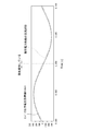
- FIG. 5 is a graph showing an example of a result obtained by simulation of a booster circuit voltage target value obtained by a control processing unit in feedback control and a booster circuit voltage detection value when controlled according to the booster circuit voltage.
- FIG. It is a figure which shows an example of an inverter output voltage target value.
- (A) is a graph comparing a booster circuit carrier wave and a booster circuit reference wave, and (b) is a drive waveform for driving the switching element Qb generated by the booster circuit control unit.
- (A) is a graph comparing the inverter circuit carrier and the inverter circuit reference wave
- (b) is a drive waveform for driving the switching element Q1 generated by the inverter circuit controller
- (c) is It is a drive waveform for driving the switching element Q3 which the inverter circuit control part produced
- It is the figure which showed an example of the current waveform of the alternating current power which an inverter apparatus outputs with an example of a reference wave and the drive waveform of each switching element.
- (A) is the graph which showed each voltage waveform of the alternating voltage output from the inverter circuit, the commercial power system, and the both-ends voltage of an AC reactor
- (b) showed the current waveform which flows into an AC reactor. It is a graph.
- FIG. 7 is a diagram illustrating an example of a current waveform of AC power output from an inverter device, together with an example of a reference wave and driving waveforms of switching elements Qb and Q1 to Q4 in the second embodiment.
- FIG. 7 is a diagram illustrating an example of a current waveform of AC power output from an inverter device, together with an example of a reference wave and driving waveforms of switching elements Qb and Q1 to Q4 in the second embodiment.
- It is an example of the circuit diagram of the inverter apparatus 1 which concerns on 3rd Embodiment. It is the figure which showed an example of the current waveform of the alternating current power which an inverter apparatus outputs with an example of the drive wave of a reference wave and a switching element in 3rd Embodiment.
- the gist of the embodiment of the present invention includes at least the following.
- This is a converter that converts DC power provided from a DC power source into AC power and supplies the load to the load, and is connected to the load, and includes a filter circuit including an AC reactor and a first capacitor; A DC / AC inverter connected to the load via the filter circuit; a DC / DC converter provided between the DC power source and the DC / AC inverter; the DC / AC inverter and the DC / DC converter; A second capacitor provided between the first capacitor, a voltage change due to the voltage of the AC power, a current flowing through the AC reactor and an impedance, a reactive current flowing through the first capacitor and the second capacitor, and the Based on the voltage of the DC power, the current target value of the DC / DC converter is synchronized with the current of the AC power. And and a control unit to have been set to.
- the DC / AC inverter and the DC / DC converter each perform high-frequency switching with the minimum number of times required.
- the AC / DC converter operates avoiding the peak of the absolute value of the AC voltage and its vicinity, and the DC / DC converter operates avoiding the zero cross of the AC voltage and its vicinity, and therefore performs high-frequency switching.
- the voltages applied to the semiconductor element and the reactor of the converter respectively become relatively low. This also contributes to the reduction of the switching loss of the semiconductor element and the iron loss of the reactor. In this way, the loss as a whole conversion device can be reduced.
- the DC / AC inverter and the DC / DC converter perform high-frequency switching alternately, and the high-frequency switching timings do not overlap. Actually, even if some overlap occurs, if there is each stop period, the loss is reduced, which contributes to higher efficiency.
- the target current value of the DC / DC converter is determined based on the AC power voltage, the voltage change due to the current flowing through the AC reactor and the impedance, the reactive current flowing through the first and second capacitors, and the DC power voltage.
- the control unit sets the output current target value to the load as Ia *, the capacitance of the first capacitor as Ca, and the voltage value of the AC power as Va.
- the DC power supply side voltage V DC and the Laplace operator is s
- the impedance of the AC reactor Za
- the larger one of the absolute values of the voltage V DC and the AC output voltage target value Vinv * of the DC / AC inverter is set as the output voltage target value Vo * of the DC / DC converter
- the capacitance of the second capacitor is C
- the conversion device (2) is an example showing a more specific control mode for realizing the conversion device (1).
- the DC / DC converter current target value Iin * reflects all of the AC power voltage, the current flowing through the AC reactor and the voltage change due to the impedance, the reactive current flowing through the first and second capacitors, and the DC power voltage. Therefore, even when the voltage of the DC power supply or the AC output current changes, it is possible to always output power synchronized with the AC output current. For this reason, the DC / DC converter and the DC / AC inverter can perform conversion from alternating current to direct current with the minimum number of times of high frequency switching. As a result, the switching loss of the semiconductor switching element and the iron loss of the AC and DC reactors are greatly reduced, and high conversion efficiency can be obtained. Furthermore, the output AC power has high quality, and a sufficiently low distortion current can be obtained for interconnection to a commercial system.
- the DC / DC converter includes a DC reactor, the voltage of the DC power supply is Vg, the impedance of the DC reactor is Z, and the current value of the DC / DC converter is Iin. (Vg ⁇ ZIin) may be the voltage V DC .
- the current value Iin of the DC / DC converter includes a value detected by a current sensor (current detection value of a DC reactor) or Iinv * ⁇ Vinv * / Vg Can be used. In the cases (3) and (4), since the voltage drop due to the current and impedance of the DC reactor is taken into consideration, accurate control can always be performed even when the current flowing through the DC / DC converter changes.
- a reference value based on a target value and a detected value of the AC output current of the DC / AC inverter, and an output voltage target of the DC / DC converter The DC / AC inverter is controlled based on a comparison of values, and the DC / AC inverter is controlled based on a comparison between a reference value based on a current target value and a detection value of the DC / DC converter and an output voltage target value of the DC / DC converter.
- / DC converter can be controlled.
- the distortion rate of the AC output current can be reduced.
- an alternating current power supply can be connected in parallel to the load.
- the converter configured as described in (6) converts the power supplied from the DC power source into AC, performs parallel operation linked to the AC power source such as a commercial power system, and supplies the AC power to the load. can do.
- electric power can be supplied from the AC power source to the DC load using the DC power source as a DC load and the load as an AC power source.
- the converter configured as described in (7) can perform conversion from alternating current to direct current.
- the DC / AC inverter operates as an AC / DC converter.
- the DC / DC converter operates as a DC / DC converter in which a current flows in a direction opposite to the conversion from direct current to alternating current.
- AC / DC converters and DC / DC converters perform high frequency switching as many times as necessary, greatly reducing the switching loss of semiconductor switching elements and the iron loss of AC reactors and DC reactors. And high conversion efficiency can be obtained.
- each calculation formula of (2) becomes a formula which gives the target value at the time of conversion from alternating current to direct current if the phase of the output current target value Ia * is inverted.
- the current target value Iin * of the DC / DC converter is a negative value with respect to the DC voltage Vg. Therefore, the conversion apparatus described in (1) to (7) can actually perform conversion from direct current to alternating current and conversion from alternating current to direct current with a common apparatus.
- a SiC element for at least one of the semiconductor switching elements included in the DC / DC converter and the DC / AC inverter.
- the conversion device described in any one of (1) to (7) can reduce the switching loss of the semiconductor element and the iron loss of the DC reactor and the AC reactor by reducing the number of high-frequency switching.
- the conduction loss of the element cannot be reduced.
- the use of the SiC element in any one of the conversion devices (1) to (7) enables high conversion due to the synergistic effect of both. Efficiency can be obtained.
- DC to AC converter with grid connection function ⁇ DC to AC converter with grid connection function
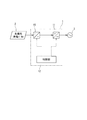
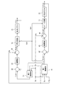
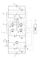
- FIG. 1 is a block diagram illustrating an example of a system including the inverter device according to the first embodiment.
- a photovoltaic power generation panel 2 as a DC power source is connected to the input terminal of the inverter device 1, and an AC commercial power system 3 (AC system) is connected to the output terminal.
- AC system AC commercial power system
- This system converts the direct current power generated by the solar power generation panel 2 into alternating current power, and performs an interconnection operation for output to the commercial power system 3.
- the inverter device 1 is a booster circuit (DC / DC converter) 10 to which DC power output from the photovoltaic power generation panel 2 is applied, and converts the power supplied from the booster circuit 10 into AC power and outputs the AC power to the commercial power system 3.
- An inverter circuit (DC / AC inverter) 11 and a control unit 12 for controlling operations of both the circuits 10 and 11 are provided.
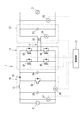
- FIG. 2 is an example of a circuit diagram of the inverter device 1.
- the booster circuit 10 includes a DC reactor 15, a diode 16, and a switching element Qb made of an IGBT (Insulated Gate Bipolar Transistor) or the like, and constitutes a boost chopper circuit.
- a first voltage sensor 17, a first current sensor 18, and a capacitor 26 for smoothing are provided on the input side of the booster circuit 10.
- the first voltage sensor 17 detects the DC input voltage detection value Vg (DC input voltage value) of the DC power output from the photovoltaic power generation panel 2 and input to the booster circuit 10, and outputs it to the control unit 12.
- Vg DC input voltage value
- the first current sensor 18 detects a booster circuit current detection value Iin (DC input current value) that is a current flowing through the DC reactor 15 and outputs it to the control unit 12. Note that a current sensor may be further provided in front of the capacitor 26 in order to detect the DC input current detection value Ig.
- the control unit 12 has a function of calculating the input power Pin from the DC input voltage detection value Vg and the booster circuit current detection value Iin and performing MPPT (Maximum Power Point Tracking) control on the photovoltaic power generation panel 2. is doing.
- the switching element Qb of the booster circuit 10 is controlled so that the total number of switching operations combined with the inverter circuit 11 is minimized, and a stop period occurs. Therefore, the booster circuit 10 outputs the boosted power to the inverter circuit 11 during the period during which the switching operation is performed, and the photovoltaic power generation panel 2 outputs the booster circuit 10 during the period during which the switching operation is stopped.
- the DC input voltage value of the DC power input to is output to the inverter circuit 11 without being boosted.
- a smoothing capacitor 19 is connected between the booster circuit 10 and the inverter circuit 11.
- the inverter circuit 11 includes switching elements Q1 to Q4 made of FET (Field Effect Transistor). These switching elements Q1 to Q4 constitute a full bridge circuit. Each of the switching elements Q1 to Q4 is connected to the control unit 12, and can be controlled by the control unit 12. The control unit 12 performs PWM control of the operations of the switching elements Q1 to Q4. Thereby, the inverter circuit 11 converts the power given from the booster circuit 10 into AC power.
- the inverter device 1 includes a filter circuit 21 between the inverter circuit 11 and the commercial power system 3.
- the filter circuit 21 includes two AC reactors 22 and a capacitor 23 (output smoothing capacitor) provided at the subsequent stage of the AC reactor 22.
- the filter circuit 21 has a function of removing high-frequency components contained in the AC power output from the inverter circuit 11. The AC power from which the high frequency component has been removed by the filter circuit 21 is supplied to the commercial power system 3.
- the booster circuit 10 and the inverter circuit 11 convert the DC power output from the photovoltaic power generation panel 2 into AC power, and output the converted AC power to the commercial power system 3 via the filter circuit 21. Part.
- the filter circuit 21 is connected to a second current sensor 24 for detecting an inverter current detection value Iinv (current flowing through the AC reactor 22), which is a current value output from the inverter circuit 11. Further, a second voltage sensor 25 for detecting a voltage value on the commercial power system 3 side (system voltage detection value Va) is connected between the filter circuit 21 and the commercial power system 3.
- the second current sensor 24 and the second voltage sensor 25 output the detected system voltage detection value Va (AC system voltage value) and the inverter current detection value Iinv to the control unit 12.
- Va AC system voltage value
- Iinv the inverter current detection value
- the control unit 12 controls the booster circuit 10 and the inverter circuit 11 based on the system voltage detection value Va and the inverter current detection value Iinv and the above-described DC input voltage detection value Vg and the booster circuit current detection value Iin.
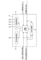
- FIG. 3 is a block diagram of the control unit 12.
- the control unit 12 functionally includes a control processing unit 30, a booster circuit control unit 32, an inverter circuit control unit 33, and an averaging processing unit 34.
- a part or all of the functions of the control unit 12 may be configured by a hardware circuit, or part or all of the functions may be realized by causing a computer (computer program) to be executed by a computer.
- Software (computer program) for realizing the function of the control unit 12 is stored in a storage device (not shown) of the computer.
- the booster circuit control unit 32 controls the switching element Qb of the booster circuit 10 based on the target value and the detection value given from the control processing unit 30, and causes the booster circuit 10 to output the electric power of the current corresponding to the target value.
- the inverter circuit control unit 33 controls the switching elements Q1 to Q4 of the inverter circuit 11 based on the target value and the detection value given from the control processing unit 30, and supplies the electric power of the current corresponding to the target value to the inverter circuit. 11 to output.
- the control processing unit 30 is provided with a DC input voltage detection value Vg, a booster circuit current detection value Iin, a system voltage detection value Va, and an inverter current detection value Iinv.
- the control processing unit 30 calculates the input power Pin and its average value ⁇ Pin> from the DC input voltage detection value Vg and the booster circuit current detection value Iin.
- the control processing unit 30 sets the DC input current target value Ig * (to be described later) based on the input power average value ⁇ Pin> to perform MPPT control on the photovoltaic power generation panel 2, and includes the booster circuit 10 and the inverter Each circuit 11 has a function of feedback control.
- the DC input voltage detection value Vg and the booster circuit current detection value Iin are given to the averaging processing unit 34 and the control processing unit 30.
- the averaging processor 34 samples the DC input voltage detection value Vg and the booster circuit current detection value Iin given from the first voltage sensor 17 and the first current sensor 18 at predetermined time intervals set in advance, respectively. And the averaged DC input voltage detection value Vg and booster circuit current detection value Iin are provided to the control processing unit 30.
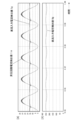
- FIG. 4 is a graph showing an example of results obtained by simulating changes with time in the DC input voltage detection value Vg and the booster circuit current detection value Iin. Further, the DC input current detection value Ig is a current value detected on the input side from the capacitor 26.
- the DC input voltage detection value Vg, the booster circuit current detection value Iin, and the DC input current detection value Ig fluctuate in a cycle of 1 ⁇ 2 of the system voltage.
- the reason why the DC input voltage detection value Vg and the DC input current detection value Ig fluctuate periodically is as follows. That is, the booster circuit current detection value Iin varies greatly from approximately 0 A to the peak value in a half cycle of the AC cycle according to the operations of the booster circuit 10 and the inverter circuit 11. Therefore, the fluctuation component cannot be completely removed by the capacitor 26, and the DC input current detection value Ig becomes a pulsating flow including a component that fluctuates in a half cycle of the AC cycle. On the other hand, the output voltage of the photovoltaic power generation panel changes depending on the output current. For this reason, the periodic fluctuation that occurs in the DC input voltage detection value Vg is 1 ⁇ 2 period of the AC power output from the inverter device 1.
- the averaging processing unit 34 averages the DC input voltage detection value Vg and the booster circuit current detection value Iin in order to suppress the influence due to the above-described periodic fluctuation.
- FIG. 5 is a diagram illustrating an aspect when the DC input voltage detection value Vg is averaged, which is performed by the averaging processing unit 34.
- the averaging processing unit 34 samples a given DC input voltage detection value Vg a plurality of times at predetermined time intervals ⁇ t in a period L from a certain timing t1 to a timing t2 (in the drawing, Black spot timing), and an average value of the obtained DC input voltage detection values Vg is obtained.
- the averaging processing unit 34 sets the period L to a length that is 1 ⁇ 2 of the periodic length of the commercial power system 3.
- the averaging processing unit 34 sets the time interval ⁇ t to a period sufficiently shorter than the length of the 1 ⁇ 2 cycle of the commercial power system 3.
- the averaging process part 34 calculates
- the sampling time interval ⁇ t can be set to, for example, 1/100 to 1/1000 of the cycle of the commercial power system 3, 20 microseconds to 200 microseconds, or the like.
- the averaging processing unit 34 can also store the period L in advance, or can acquire the system voltage detection value Va from the second voltage sensor 25 and set the period L based on the cycle of the commercial power system 3. You can also In addition, here, the period L is set to 1 ⁇ 2 the period length of the commercial power system 3, but if the period L is set to at least a 1 ⁇ 2 period of the commercial power system 3, the DC input The average value of the voltage detection value Vg can be obtained with high accuracy. This is because the DC input voltage detection value Vg periodically fluctuates with a length of 1 ⁇ 2 of the cycle length of the commercial power system 3 due to the operations of the booster circuit 10 and the inverter circuit 11 as described above.
- the period L is set to an integral multiple of the 1/2 cycle of the commercial power system 3, such as 3 or 4 times the 1/2 cycle of the commercial power system 3. do it.
- the voltage fluctuation can be grasped in units of cycles.
- the booster circuit current detection value Iin also periodically fluctuates in a half cycle of the commercial power system 3, as with the DC input voltage detection value Vg. Therefore, the averaging processing unit 34 also obtains an average value of the booster circuit current detection value Iin by a method similar to the DC input voltage detection value Vg shown in FIG.
- the control processing unit 30 sequentially obtains the average value of the DC input voltage detection value Vg and the average value of the booster circuit current detection value Iin for each period L.
- the averaging processing unit 34 gives the average value of the obtained DC input voltage detection value Vg and the average value of the boost circuit current detection value Iin to the control processing unit 30.
- the averaging processing unit 34 performs the average value of the DC input voltage detection value Vg (DC input voltage average value ⁇ Vg>) and the average value of the boost circuit current detection value Iin (boost circuit current).
- the average value ⁇ Iin>) is obtained, and the control processing unit 30 uses these values to control the booster circuit 10 and the inverter circuit 11 while performing MPPT control on the solar power generation panel 2, and thus the solar power generation panel 2
- the control unit 12 uses the DC input voltage average value ⁇ Vg> from which the fluctuation component due to the operation of the inverter device 1 is removed and the booster circuit. It can be accurately obtained as the current average value ⁇ Iin>.
- MPPT control can be performed suitably and it can suppress effectively that the power generation efficiency of the photovoltaic power generation panel 2 falls.
- the DC input voltage average value ⁇ Vg> and the booster circuit current average value ⁇ Iin> were obtained from the results, the DC current voltage and current Even if the frequency fluctuates periodically, the DC input voltage average value ⁇ Vg> and the booster circuit current average value ⁇ Iin> can be obtained with high accuracy while shortening the sampling period as much as possible.
- the control processing unit 30 sets the DC input current target value Ig * based on the above-described input power average value ⁇ Pin>, and based on the set DC input current target value Ig * and the above value, the booster circuit 10 and the target values for the inverter circuit 11 are obtained.
- the control processing unit 30 has a function of giving the obtained target value to the booster circuit control unit 32 and the inverter circuit control unit 33 and performing feedback control of the booster circuit 10 and the inverter circuit 11 respectively.
- FIG. 6 is a control block diagram for explaining feedback control of the booster circuit 10 and the inverter circuit 11 by the control processing unit 30.
- the control processing unit 30 includes a first calculation unit 41, a first adder 42, a compensator 43, and a second adder 44 as functional units for controlling the inverter circuit 11.
- the control processing unit 30 includes a second calculation unit 51, a third adder 52, a compensator 53, and a fourth adder 54 as functional units for controlling the booster circuit 10.
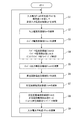
- FIG. 7 is a flowchart showing control processing of the booster circuit 10 and the inverter circuit 11.
- Each functional unit illustrated in FIG. 6 controls the booster circuit 10 and the inverter circuit 11 by executing the processing illustrated in the flowchart illustrated in FIG.
- control processing of the booster circuit 10 and the inverter circuit 11 will be described with reference to FIG.
- control processing unit 30 obtains the current input power average value ⁇ Pin> (step S9) and compares it with the input power average value ⁇ Pin> at the previous calculation to set the DC input current target value Ig *. (Step S1).
- the input power average value ⁇ Pin> is obtained based on the following formula (1).
- Input power average value ⁇ Pin> ⁇ Iin ⁇ Vg> (1)
- Iin is a boost circuit current detection value
- Vg is a DC input voltage detection value (DC input voltage value)
- a DC input voltage average value that is an averaged value by the averaging processing unit 34.
- ⁇ Vg> and the booster circuit current average value ⁇ Iin> are used.
- instantaneous values that are not averaged are used for the booster circuit current detection value Iin and the DC input voltage detection value Vg.
- ⁇ > Indicates an average value in parentheses. The same applies hereinafter.
- the control processing unit 30 gives the set DC input current target value Ig * to the first calculation unit 41.
- the first calculation unit 41 is also provided with a DC input voltage detection value Vg and a system voltage detection value Va.
- the first calculation unit 41 calculates an average value ⁇ Ia *> of the output current target value as the inverter device 1 based on the following formula (2).
- ⁇ is a constant representing the conversion efficiency of the inverter device 1.
- Average output current target value ⁇ Ia *> ⁇ ⁇ Ig * ⁇ Vg> / ⁇ Va> ...
- the first calculation unit 41 obtains the output current target value Ia * based on the following formula (3) (step S2).
- the first calculation unit 41 obtains the output current target value Ia * as a sine wave having the same phase as the system voltage detection value Va.
- Output current target value Ia * ( ⁇ 2) ⁇ ⁇ Ia *> ⁇ sin ⁇ t ... (3)
- Ca is the electrostatic capacitance of the capacitor
- condenser 23 output smoothing capacitor
- the output current target value Ia * is obtained as a sine wave having the same phase as the system voltage detection value Va, as shown in the above equation (3). That is, the control processing unit 30 controls the inverter circuit 11 so that the current Ia (output current) of the AC power output from the inverter device 1 is in phase with the system voltage (system voltage detection value Va).
- the first calculation unit 41 When the first calculation unit 41 obtains the inverter current target value Iinv *, it supplies the inverter current target value Iinv * to the first adder 42.
- the inverter circuit 11 is feedback-controlled by this inverter current target value Iinv *.
- the current adder current detection value Iinv is given to the first adder 42.
- the first adder 42 calculates the difference between the inverter current target value Iinv * and the current inverter current detection value Iinv, and gives the calculation result to the compensator 43.
- the compensator 43 When the difference is given, the compensator 43 performs an operation based on a proportional coefficient and the like, and further adds the system voltage Va by the second adder 44, thereby converging the difference and converting the inverter current detection value Iinv into the inverter.
- An inverter voltage reference value Vinv # that can be used as the current target value Iinv * is obtained.
- the inverter circuit control unit 33 By giving the inverter circuit control unit 33 a control signal obtained by comparing the inverter voltage reference value Vinv # with the output voltage target value Vo * of the DC / DC converter supplied from the first calculation unit 41, the inverter circuit 11 To output a voltage according to the inverter voltage reference value Vinv #.
- the voltage output from the inverter circuit 11 is given to the AC reactor 22 and fed back as a new inverter current detection value Iinv. Then, the difference between the inverter current target value Iinv * and the inverter current detection value Iinv is calculated again by the first adder 42, and the inverter circuit 11 is controlled based on this difference as described above.
- the inverter circuit 11 is feedback-controlled by the inverter current target value Iinv * and the inverter current detection value Iinv (step S4).
- the inverter current target value Iinv * calculated by the first calculation unit 41 is given to the second calculation unit 51.
- the second calculation unit 51 calculates the inverter output voltage target value Vinv * (voltage target value of the inverter circuit) based on the following formula (5) (step S5).
- Inverter output voltage target value Vinv * Va + ZaIinv * ... (5)
- the inverter current target value which is a current target value for controlling the inverter circuit 11 so that the current phase of the AC power output from the inverter device 1 is in phase with the system voltage detection value Va.
- An inverter output voltage target value Vinv * is set based on Iinv *.
- the output target value (Iinv *, Vinv *) of the inverter circuit 11 that is the target value on the AC side is the bridge output terminal of the inverter circuit 11, that is, the circuit connection point P between the inverter circuit 11 and the filter circuit 21.
- the system connection point where the set point of the target value is moved forward from the original system connection point (the circuit connection point between the commercial power system 3 and the filter circuit 21) and finally settles into an appropriate system connection point. The system is done.
- the second calculation unit 51 When the inverter output voltage target value Vinv * is obtained, as shown in the following formula (6), the second calculation unit 51 generates the voltage Vg as the voltage V DC on the DC power supply side or preferably the following DC voltage Vgf and the inverter The absolute value of the output voltage target value Vinv * is compared, and the larger one is determined as the boost circuit voltage target value Vo * (step S6).
- Vo * Max (Vg ⁇ (RIin + L (d Iin / dt), absolute value of Vinv *) ... (6a) It is.
- R is the resistance of the DC reactor
- L is the inductance of the DC reactor
- (Z R + sL).
- the second calculation unit 51 calculates the boost circuit current target value Iin * based on the following equation (7) (step S7).
- Boost circuit current target value Iin * ⁇ (Iinv * ⁇ Vinv *) + (s C Vo *) ⁇ Vo * ⁇ / (Vg ⁇ ZIin) ... (7)
- C is the electrostatic capacitance of the capacitor
- the term added to the product of the inverter current target value Iinv * and the inverter output voltage target value Vinv * takes into account reactive power passing through the capacitor 19 Value. That is, the value of Iin * can be obtained more accurately by considering reactive power in addition to the power target value of the inverter circuit 11.
- the above equation (7a) can also be expressed as follows.
- Iin * ⁇ (Iinv * ⁇ Vinv *) + C ⁇ (d Vo * / dt) ⁇ Vo * + P LOSS ⁇ / ⁇ Vg-ZIin ⁇ ⁇ (7c)
- the above formula (7b) can also be expressed as follows.
- Iin * ⁇ (Iinv * ⁇ Vinv *) + Ic ⁇ Vo * + P LOSS ⁇ / ⁇ Vg ⁇ ZIin ⁇ ... (7d)
- the value of Iin * can be determined more strictly by considering the reactive power and the power loss P LOSS .
- the second calculation unit 51 When the second calculation unit 51 obtains the booster circuit current target value Iin *, it supplies the booster circuit current target value Iin * to the third adder 52.
- the booster circuit 10 is feedback-controlled by this booster circuit current target value Iin *.
- the current booster circuit current detection value Iin is given to the third adder 52.
- the third adder 52 calculates the difference between the booster circuit current target value Iin * and the current booster circuit current detection value Iin, and gives the calculation result to the compensator 53.
- the compensator 53 When the difference is given, the compensator 53 performs a calculation based on a proportional coefficient and the like, and further subtracts this from the DC input voltage detection value Vg by the fourth adder 54, thereby converging the difference and boosting the circuit.
- a booster circuit voltage reference value Vbc # that can make the current detection value Iin the booster circuit current target value Iin * is obtained.
- the boost circuit control unit 32 By giving the boost circuit control unit 32 a control signal obtained by comparing the boost circuit voltage reference value Vbc # with the output voltage target value Vo * of the DC / DC converter supplied from the first calculation unit 41, the boost circuit 10, the voltage according to the booster circuit voltage reference value Vbc # is output.
- the electric power output from the booster circuit 10 is given to the DC reactor 15 and fed back as a new booster circuit current detection value Iin. Then, the difference between the booster circuit current target value Iin * and the booster circuit current detection value Iin is calculated again by the third adder 52, and the booster circuit 10 is controlled based on this difference as described above.
- the booster circuit 10 is feedback controlled by the booster circuit current target value Iin * and the booster circuit current detection value Iin (step S8).
- step S8 the control processing unit 30 obtains the current input power average value ⁇ Pin> based on the above equation (1) (step S9).
- the control processing unit 30 compares the input power average value ⁇ Pin> at the previous calculation with the DC input current so that the input power average value ⁇ Pin> becomes the maximum value (follows the maximum power point). Set the target value Ig *.
- control processing unit 30 controls the booster circuit 10 and the inverter circuit 11 while performing MPPT control on the photovoltaic power generation panel 2.
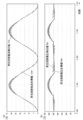
- FIG. 8A is a graph showing an example of a result obtained by simulation of the booster circuit current target value Iin * obtained by the control processing unit 30 in the feedback control and the booster circuit current detection value Iin when controlled according to the target value.
- (B) shows an example of a result obtained by simulation of the booster circuit voltage target value Vo * obtained by the control processing unit 30 in the feedback control and the booster circuit voltage detection value Vo when controlled according to the booster circuit voltage. It is a graph.
- the boost circuit current detection value Iin is controlled by the control processing unit 30 along the boost circuit current target value Iin *.
- the booster circuit voltage target value Vo * is obtained by the above equation (6), the absolute value of the inverter output voltage target value Vinv * is approximately equal to the DC input voltage detection value Vg. In the period described above, it changes so as to follow the absolute value of the inverter output voltage target value Vinv *, and to follow the DC input voltage detection value Vg in other periods. It can be seen that the booster circuit voltage detection value Vo is controlled by the control processing unit 30 along the booster circuit voltage target value Vo *.
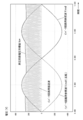
- FIG. 9 is a diagram illustrating an example of the inverter output voltage target value Vinv *.
- the vertical axis represents voltage and the horizontal axis represents time.
- the broken line indicates the voltage waveform of the commercial power system 3
- the solid line indicates the waveform of the inverter output voltage target value Vinv *.
- the inverter circuit 11 outputs power with the inverter output voltage target value Vinv * shown in FIG. 9 as the voltage target value by the control according to the flowchart of FIG. Therefore, the inverter circuit 11 outputs the electric power of the voltage according to the waveform of the inverter output voltage target value Vinv * shown in FIG.
- both waves have substantially the same voltage value and frequency, but the phase of the inverter output voltage target value Vinv * is advanced several times with respect to the voltage phase of the commercial power system 3. ing.
- the control processing unit 30 of the present embodiment changes the phase of the inverter output voltage target value Vinv * to the voltage phase of the commercial power system 3 while executing the feedback control of the booster circuit 10 and the inverter circuit 11.
- the phase is advanced about 3 degrees.
- the angle by which the phase of the inverter output voltage target value Vinv * is advanced with respect to the voltage phase of the commercial power system 3 may be several degrees, and is different from the voltage waveform of the commercial power system 3 as will be described later. Is set in a range where the phase is advanced by 90 degrees with respect to the voltage waveform of the commercial power system 3. For example, it is set in a range of values larger than 0 degree and smaller than 10 degrees.
- the phase advance angle is determined by the system voltage detection value Va, the inductance La of the AC reactor 22, and the inverter current target value Iinv * as shown in the above equation (5).
- the system voltage detection value Va and the inductance La of the AC reactor 22 are fixed values that are not controlled, and therefore the phase advance angle is determined by the inverter current target value Iinv *.
- the inverter current target value Iinv * is determined by the output current target value Ia * as shown in the above equation (4). As the output current target value Ia * increases, the phase-advanced component of the inverter current target value Iinv * increases, and the advance angle (angle to advance) of the inverter output voltage target value Vinv * increases.
- the booster circuit control unit 32 controls the switching element Qb of the booster circuit 10.
- the inverter circuit control unit 33 controls the switching elements Q1 to Q4 of the inverter circuit 11.
- the booster circuit control unit 32 and the inverter circuit control unit 33 generate a booster circuit carrier wave and an inverter circuit carrier wave, respectively, and these carrier waves are booster circuit voltage reference values Vbc # that are target values given from the control processing unit 30, and Modulation is performed using the inverter voltage reference value Vinv # to generate a drive waveform for driving each switching element.
- the step-up circuit control unit 32 and the inverter circuit control unit 33 control each switching element based on the drive waveform, whereby an alternating current waveform approximate to the step-up circuit current target value Iin * and the inverter current target value Iinv *. Electric power is output to the booster circuit 10 and the inverter circuit 11.
- FIG. 10A is a graph comparing the booster carrier and the waveform of the booster circuit voltage reference value Vbc #.
- the vertical axis represents voltage and the horizontal axis represents time.
- the wavelength of the booster carrier wave is shown longer than the actual wavelength.
- the booster circuit carrier wave generated by the booster circuit control unit 32 is a triangular wave whose local minimum value is “0”, and the amplitude A1 is the booster circuit voltage target value Vo * given from the control processing unit 30.
- the frequency of the booster circuit carrier wave is set by the booster circuit control unit 32 according to a control command from the control processing unit 30 so as to have a predetermined duty ratio.
- the booster circuit voltage target value Vo * is equal to the inverter output voltage target value Vinv * during the period W1 in which the absolute value of the inverter output voltage target value Vinv * is approximately equal to or greater than the DC input voltage detection value Vg. Following the absolute value, it changes so as to follow the DC input voltage detection value Vg in the other periods. Therefore, the amplitude A1 of the booster circuit carrier also changes according to the booster circuit voltage target value Vo *.
- the waveform of the booster circuit voltage reference value Vbc # (hereinafter also referred to as booster circuit reference wave Vbc #) is a value obtained by the control processing unit 30 based on the booster circuit current target value Iin *, and is the inverter output voltage target value Vinv.
- the absolute value of * is a positive value in a period W1 in which the absolute value is larger than the DC input voltage detection value Vg.
- the booster circuit reference wave Vbc # has a waveform that approximates the waveform formed by the booster circuit voltage target value Vo *, and intersects the booster carrier wave.
- the booster circuit control unit 32 compares the booster circuit carrier wave with the booster circuit reference wave Vbc #, and the booster circuit reference wave Vbc #, which is the target value of the voltage across the DC reactor 15, becomes equal to or higher than the booster circuit carrier wave.
- a drive waveform for driving the switching element Qb is generated so as to be turned on in the portion and turned off in the portion below the carrier wave.
- FIG. 10B shows a drive waveform for driving the switching element Qb generated by the booster circuit control unit 32.
- the vertical axis represents voltage and the horizontal axis represents time.
- the horizontal axis is shown to coincide with the horizontal axis of FIG.
- This drive waveform indicates the switching operation of the switching element Qb, and by applying it to the switching element Qb, the switching operation according to the drive waveform can be executed.
- the drive waveform constitutes a control command that turns off the switching element when the voltage is 0 volts and turns on the switching element when the voltage is positive.
- the booster circuit control unit 32 generates a drive waveform so that the switching operation is performed in a period W1 in which the absolute value of the inverter output voltage target value Vinv * is equal to or greater than the DC input voltage detection value Vg. Therefore, the switching element Qb is controlled so as to stop the switching operation within the range of the DC input voltage detection value Vg or less.
- Each pulse width is determined by the intercept of the carrier wave for the booster circuit which is a triangular wave. Therefore, the pulse width increases as the voltage increases.
- the booster circuit control unit 32 modulates the booster circuit carrier wave with the booster circuit reference wave Vbc #, and generates a drive waveform representing the pulse width for switching.
- the booster circuit control unit 32 performs PWM control of the switching element Qb of the booster circuit 10 based on the generated drive waveform.
- the switching element Qbu When the switching element Qbu that conducts in the forward direction of the diode in parallel with the diode 16 is installed, the switching element Qbu uses a driving waveform that is inverted from the driving waveform of the switching element Qb. However, in order to prevent the switching element Qb and the switching element Qbu from conducting simultaneously, a dead time of about 1 microsecond is provided when the drive pulse of the switching element Qbu shifts from OFF to ON.
- FIG. 11A is a graph comparing the inverter circuit carrier with the waveform of the inverter voltage reference value Vinv #.
- the vertical axis represents voltage and the horizontal axis represents time.
- the wavelength of the carrier wave for the inverter circuit is shown longer than the actual wavelength for easy understanding.
- the inverter circuit carrier generated by the inverter circuit control unit 33 is a triangular wave having an amplitude center of 0 volts, and its one-side amplitude is set to the boost circuit voltage target value Vo * (the voltage target value of the capacitor 23). Therefore, the amplitude A2 of the carrier wave for the inverter circuit has a period that is twice (500 volts) the detected DC input voltage value Vg and a period that is twice the voltage of the commercial power system 3 (maximum 576 volts). . Further, the frequency is set by the inverter circuit control unit 33 so as to have a predetermined duty ratio by a control command or the like by the control processing unit 30.
- the booster circuit voltage target value Vo * is equal to the inverter output voltage target value Vinv * during the period W1 in which the absolute value of the inverter output voltage target value Vinv * is approximately equal to or greater than the DC input voltage detection value Vg.
- the amplitude A2 of the inverter circuit carrier also changes in accordance with the boost circuit voltage target value Vo *.
- the waveform of the inverter voltage reference value Vinv # (hereinafter also referred to as the inverter circuit reference wave Vinv #) is a value obtained by the control processing unit 30 based on the inverter current target value Iinv *, and is generally a voltage amplitude of the commercial power system 3. It is set to be the same as (288 volts). Therefore, the inverter circuit reference wave Vinv # intersects the booster circuit carrier in a portion where the voltage value is in the range of ⁇ Vg to + Vg.
- the inverter circuit control unit 33 compares the inverter circuit carrier wave with the inverter circuit reference wave Vinv #, and is turned on when the inverter circuit reference wave Vinv #, which is the voltage target value, is greater than or equal to the inverter circuit carrier wave.
- a drive waveform for driving the switching elements Q1 to Q4 is generated so as to be turned off at a portion where
- FIG. 11B shows a drive waveform for driving the switching element Q ⁇ b> 1 generated by the inverter circuit control unit 33.
- the vertical axis represents voltage and the horizontal axis represents time.
- the horizontal axis is shown so as to coincide with the horizontal axis of FIG.
- the inverter circuit control unit 33 generates a drive waveform so that the switching operation is performed in the range W2 where the voltage of the inverter circuit reference wave Vinv # is in the range of ⁇ Vg to + Vg. Therefore, in the other range, the switching element Q1 is controlled so as to stop the switching operation.
- FIG. 11C shows a drive waveform for driving the switching element Q3 generated by the inverter circuit control unit 33.
- the vertical axis represents voltage and the horizontal axis represents time.
- the inverter circuit control unit 33 compares the inverted wave of the inverter circuit reference wave Vinv # indicated by the broken line in the drawing with a carrier wave to generate a drive waveform. Also in this case, the inverter circuit control unit 33 generates the drive waveform so that the switching operation is performed in the range W2 where the voltage of the inverter circuit reference wave Vinv # (inverted wave thereof) is ⁇ Vg to + Vg. Therefore, in the other range, the switching element Q3 is controlled so as to stop the switching operation.
- the inverter circuit control unit 33 generates the inverted driving waveform of the switching element Q1 for the driving waveform of the switching element Q2, and inverts the driving waveform of the switching element Q3 for the driving waveform of the switching element Q4.
- the inverter circuit control unit 33 modulates the inverter circuit carrier wave with the inverter circuit reference wave Vinv #, and generates a drive waveform representing a pulse width for switching.
- the inverter circuit control unit 33 performs PWM control on the switching elements Q1 to Q4 of the inverter circuit 11 based on the generated drive waveform.
- the booster circuit control unit 32 of the present embodiment outputs power so that the current flowing through the DC reactor 15 matches the booster circuit current target value Iin *.
- the booster circuit 10 is caused to perform a switching operation in a period W1 (FIG. 10) in which the absolute value of the inverter output voltage target value Vinv * is approximately equal to or greater than the DC input voltage detection value Vg.
- the booster circuit 10 outputs power so that a voltage equal to or greater than the DC input voltage detection value Vg is approximated to the absolute value of the inverter output voltage target value Vinv * in the period W1.
- the booster circuit control unit 32 stops the switching operation of the booster circuit 10. Therefore, during the period equal to or less than the DC input voltage detection value Vg, the booster circuit 10 outputs the DC input voltage value of the DC power output from the photovoltaic power generation panel 2 to the inverter circuit 11 without boosting.
- the inverter circuit control part 33 of this embodiment outputs electric power so that the electric current which flows into the AC reactor 22 may correspond to inverter electric current target value Iinv *.
- the inverter circuit 11 is caused to perform a switching operation in a period W2 (FIG. 11) in which the inverter output voltage target value Vinv * is approximately ⁇ Vg to + Vg. That is, the inverter circuit 11 is caused to perform a switching operation in a period in which the absolute value of the inverter output voltage target value Vinv * is equal to or less than the DC input voltage detection value Vg.
- the inverter circuit 11 performs the switching operation while the booster circuit 10 stops the switching operation, and outputs AC power approximate to the inverter output voltage target value Vinv *. Since the inverter circuit reference wave Vinv # and the inverter output voltage target value Vinv * are approximated, they overlap in FIG.
- the inverter circuit control unit 33 stops the switching operation of the inverter circuit 11 in a period other than the period W2 in which the voltage of the inverter output voltage target value Vinv * is approximately ⁇ Vg to + Vg. During this time, the inverter circuit 11 is supplied with the electric power boosted by the booster circuit 10. Therefore, the inverter circuit 11 that has stopped the switching operation outputs the power supplied from the booster circuit 10 without stepping down.
- the inverter device 1 approximates the inverter output voltage target value Vinv * by switching the booster circuit 10 and the inverter circuit 11 so as to be switched alternately and superimposing the electric power output by each. Output AC power with voltage waveform.
- the booster circuit 10 when the absolute value of the inverter output voltage target value Vinv * is higher than the DC input voltage detection value Vg, the booster circuit 10 is operated, and the inverter output voltage target Control is performed so that the inverter circuit 11 is operated when the voltage of the portion where the absolute value of the value Vinv * is lower than the DC input voltage detection value Vg is output. Therefore, since the inverter circuit 11 does not step down the power boosted by the booster circuit 10, the potential difference when the voltage is stepped down can be kept low, so that the loss due to switching of the booster circuit can be reduced and higher. AC power can be output with high efficiency.
- both the booster circuit 10 and the inverter circuit 11 operate based on the inverter output voltage target value Vinv * set by the control unit 12, the booster circuit power output so as to be switched alternately and the inverter circuit power It is possible to suppress the occurrence of displacement and distortion between the two.
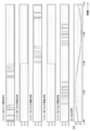
- FIG. 12 is a diagram illustrating an example of a current waveform of AC power output from the inverter device 1 together with an example of a reference wave and a driving waveform of a switching element.
- the reference wave Vinv # and carrier wave of the inverter circuit, the driving waveform of the switching element Q1, the reference wave Vbc # and carrier wave of the booster circuit, the driving waveform of the switching element Qb, and the inverter device 1 are output in order from the top.
- the graph which shows the target value and measured value of the current waveform of alternating current power is represented.
- the horizontal axis of each graph indicates time and is shown to coincide with each other.
- the actual measured value Ia of the output current is controlled to coincide with the target value Ia *. It can also be seen that the period of switching operation of the switching element Qb of the booster circuit 10 and the period of switching operation of the switching elements Q1 to Q4 of the inverter circuit 11 are controlled to be switched alternately.
- the booster circuit obtained based on the above equation (7) is controlled so that the current flowing through the DC reactor 15 matches the current target value Iin *. .
- the voltages of the booster circuit and the inverter circuit have the waveforms shown in FIG. 8B, and the high-frequency switching operations of the booster circuit 10 and the inverter circuit 11 each have a stop period, and the operation of performing the switching operation almost alternately is performed. It becomes possible.
- the booster circuit 10 and the inverter circuit 11 perform “alternately” high-frequency switching so that the high-frequency switching timings do not overlap. If there is a period, the loss is reduced, which contributes to higher efficiency.
- the booster circuit 10 and the inverter circuit 11 output AC power having a voltage waveform approximate to the inverter output voltage target value Vinv * to the filter circuit 21 connected to the subsequent stage under the control of the control unit 12.
- the inverter device 1 outputs AC power to the commercial power system 3 via the filter circuit 21.
- the inverter output voltage target value Vinv * is generated as a voltage phase advanced by the control processor 30 several times with respect to the voltage phase of the commercial power system 3 as described above. Therefore, the AC voltage output from the booster circuit 10 and the inverter circuit 11 is also a voltage phase advanced by several degrees with respect to the voltage phase of the commercial power system 3.
- the AC reactor 22 (FIG. 2) of the filter circuit 21 is applied to both ends of the AC voltage of the booster circuit 10 and the inverter circuit 11 on one side and the commercial power system 3 on the other side. It will be different.
- FIG. 13A is a graph showing the voltage waveforms of the AC voltage output from the inverter circuit 11, the commercial power system 3, and the voltage across the AC reactor 22, respectively.
- the vertical axis represents voltage and the horizontal axis represents time.
- the voltage of both ends of the AC reactor 22 is a voltage applied to both ends of the AC reactor 22. Difference.
- the phase of the voltage across the AC reactor 22 is advanced by 90 degrees with respect to the voltage phase of the commercial power system 3.
- FIG. 13B is a graph showing a waveform of a current flowing through the AC reactor 22.
- the vertical axis represents current and the horizontal axis represents time.
- the horizontal axis is shown so as to coincide with the horizontal axis in FIG.
- the current phase of AC reactor 22 is delayed by 90 degrees with respect to the voltage phase. Therefore, as shown in the figure, the current phase of the AC power output through the AC reactor 22 is synchronized with the current phase of the commercial power system 3.
- the voltage phase output from the inverter circuit 11 is advanced several times with respect to the commercial power system 3, but the current phase matches the current phase of the commercial power system 3. Therefore, the current waveform output from the inverter device 1 coincides with the voltage phase of the commercial power system 3 as shown in the graph shown at the bottom of FIG. As a result, since an alternating current having the same phase as the voltage of the commercial power system 3 can be output, it is possible to suppress a reduction in the power factor of the alternating power.
- Fig.22 (a) is an example of the alternating current output waveform of the inverter apparatus 1 which concerns on 1st Embodiment.
- the booster circuit current target value Iin * in this case is given by, for example, Expression (7).
- a sinusoidal AC output current synchronized with the system voltage is obtained.
- the power factor at this time is 0.997, and the total current distortion factor is 4.6%, which is in conformity with the reference value of the grid connection generally set to 0.95 or more and 5% or less.
- the second order distortion is 2.6% (conforming to 3% or less)
- the third order distortion is 2.9% (conforming to 3% or less)
- the fifth order distortion is 0.3% (3%). It conforms to the following).
- FIG. 22B is an example of an AC output waveform obtained when the inverter device 1 is controlled in accordance with the boost circuit current target value defined by the following equation (9) described in Patent Document 2 described above. is there.
- Iin * Ia * ⁇ Va / Vg (9)
- the AC output current has a waveform whose peak is clearly distorted, the power factor is 0.947 (not suitable for 0.95 or more), and the total current distortion rate is 8.3% (not suitable for 5% or less). Yes, none of them meet the above grid connection reference values.
- the second order distortion is 3.5% (not suitable for 3% or less)
- the third order distortion is 4.3% (not suitable for 3% or less)
- the fifth order distortion is 4.6% (3%). (Not compatible with the following).
- FIG. 14 is an example of a circuit diagram of the inverter device 1 according to the second embodiment.
- the difference between the present embodiment and the first embodiment is that an IGBT is used as the switching elements Q1 to Q4 of the inverter circuit 11.
- Other configurations are the same as those of the first embodiment.
- the inverter circuit control unit 33 uses a carrier wave different from the inverter circuit carrier wave used in the first embodiment.
- FIG. 15 is a graph comparing the inverter circuit carrier and the reference wave in the second embodiment. In the figure, the vertical axis represents voltage and the horizontal axis represents time. The reference wave and the booster carrier are the same as in the first embodiment.
- the inverter circuit carrier of the present embodiment is a triangular wave having a lower limit set to 0 volts and an upper limit set to the boost circuit voltage target value Vo *.
- the inverter circuit control unit 33 generates the drive waveform of the switching element Q1 by comparing the inverter circuit reference wave Vinv # with the inverter circuit carrier wave, and the drive waveform of the switching element Q3 is the inverter circuit. It is generated by comparing the inverted wave of the reference wave Vinv # for use with the carrier wave for the inverter circuit.
- the inverter circuit control unit 33 compares the inverter circuit carrier (booster circuit carrier) with the inverter circuit reference wave Vinv #, and the inverter that is the voltage target value.
- FIG. 16 is a diagram illustrating an example of a current waveform of AC power output from the inverter device 1 along with an example of a drive waveform of each switching element Qb, Q1 to Q4 in the second embodiment.
- the driving waveform of the switching element Q1, the driving waveform of the switching element Q4, the driving waveform of the switching element Q3, the driving waveform of the switching element Q2, the driving waveform of the switching element Qb, and the inverter device 1 are output in order from the top.
- the graph which shows the electric current waveform of AC electric power to perform is shown.
- the horizontal axis of each graph indicates time and is shown to coincide with each other.
- the switching element Q1 and the switching element Q3 are controlled to perform switching when the voltage of the inverter circuit reference wave Vinv # is in the range of ⁇ Vg to + Vg. Also in the present embodiment, as shown in the figure, the period of switching operation of the switching element Qb of the booster circuit 10 and the period of switching operation of the switching elements Q1 to Q4 of the inverter circuit 11 are controlled so as to be alternately switched. It can be seen that
- the current waveform of the AC power output from the inverter device 1 of the present embodiment is the same as the voltage phase of the commercial power system 3 as shown in FIG. Therefore, similarly to the first embodiment, AC power having the same phase as the current phase can be output to the commercial power system 3, and the power factor of the AC power can be prevented from being lowered.
- FIG. 17 is an example of a circuit diagram of the inverter device 1 according to the third embodiment.
- the difference between the present embodiment and the first embodiment is that a third voltage sensor 27 that detects an intermediate voltage between the booster circuit 10 and the inverter circuit 11 is provided.
- Other configurations are the same as those of the first embodiment.
- the booster circuit voltage target value Vo * (target value of the intermediate voltage) is used as the amplitude of the carrier wave.
- the voltage detection value Vo detected by the third voltage sensor 27 is used as the carrier wave amplitude. Used for.
- FIG. 18 is a diagram illustrating an example of a current waveform of AC power output from the inverter device 1 together with an example of a reference wave and a driving waveform of a switching element in the third embodiment.
- the reference wave Vinv # and carrier wave of the inverter circuit, the driving waveform of the switching element Q1, the reference wave Vbc # and carrier wave of the booster circuit, the driving waveform of the switching element Qb, and the inverter device 1 are output in order from the top.
- the graph which shows the target value Ia * and the actual measurement value Ia of the current waveform of alternating current power is represented.
- the horizontal axis of each graph indicates time and is shown to coincide with each other.
- the measured value Ia of the output current is also controlled to match the target value Ia * in this embodiment.
- the switching operation period of the switching element Qb of the booster circuit 10 and the switching operation period of the switching element Q1 of the inverter circuit 11 are controlled to be switched alternately.
- the voltage detection value Vo for the amplitude of the carrier wave as in the present embodiment, the response when the voltage of the photovoltaic power generation panel 2 or the commercial power system 3 fluctuates becomes faster, and the inverter device 1 The output current can be stabilized.
- FIG. 19 is a block diagram illustrating an example of a power storage system including such a conversion device 1R.
- the storage battery 2 is connected to the output terminal of the converter 1R, and the commercial power system 3 (AC system) is connected to the input terminal.
- the power storage system can convert the power provided from the commercial power system 3 from AC to DC and store it in the storage battery 2.
- the converter 1R includes an AC / DC converter 11u that converts alternating current received from the commercial power system 3 into direct current, a step-down circuit (DC / DC converter) 10d that steps down the output voltage of the AC / DC converter 11u, and both of these circuits. And a control unit 12 that controls operations of the motors 10 and 11. As is clear from comparison with FIG. 1, the energy flow is in the opposite direction.
- FIG. 20 is an example of a circuit diagram of the conversion device 1R.
- the difference from FIG. 2, FIG. 14, FIG. 17 (hereinafter referred to as FIG. 2 etc.) is that the solar power generation panel 2 in FIG. 2 etc. is replaced with a storage battery 2B.
- the step-up circuit 10 in FIG. 2 and the like is replaced with the step-down circuit 10d, and the circuit that is the inverter circuit 11 in FIG. 2 and the like has the same components but cooperates with the AC reactor 22.
- the AC / DC converter 11u can be boosted.
- the step-down circuit 10d uses a switching element Qb2 in parallel with the diode 16 similar to FIG.
- the switching element Qb2 for example, the illustrated IGBT or FET can be used.
- the conversion device 1R is bidirectional, and can perform the same operation as the inverter device 1 shown in FIG.
- the DC power of the storage battery 2B can be converted into AC power for independent operation.
- the switching element Qb2 is always turned off (in the case of IGBT) or alternately turned on with the switching element Qb (in the case of FET). It is controlled by the control unit 12.
- the step-down circuit 10d is a step-up circuit
- the AC / DC converter 11u is an inverter circuit.
- the control unit 12 can control the operations of the switching elements Q1 to Q4 to perform synchronous rectification. Further, by performing PWM control in the presence of the AC reactor 22, rectification can be performed while boosting. Thus, the AC / DC converter 11u converts the AC power supplied from the commercial AC system 3 into DC power.
- the step-down circuit 10d constitutes a step-down chopper circuit.
- the switching elements Qb and Qb2 are controlled by the control unit 12. Further, the switching operation of the step-down circuit 10d is controlled so that the period for performing the switching operation with the AC / DC converter 11u is alternately switched. Therefore, the step-down circuit 10d outputs the stepped-down voltage to the storage battery 2B during the period when the switching operation is performed, and stops the switching operation (the switching element Qb is off and Qb2 is on).
- the DC voltage output from the DC converter 11u and input to the step-down circuit 10d is applied to the storage battery 2 via the DC reactor 15.
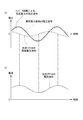
- FIG. 21 is a voltage waveform diagram conceptually showing the operation of the converter 1R.
- (A) shows an example of the absolute value of the AC input voltage target value Vinv * to the AC / DC converter 11u. This is generally a commercial AC full-wave rectified waveform.
- a two-dot chain line indicates a DC voltage Vg for charging.
- the AC / DC converter 11u performs a switching operation in a section (t0 to t1, t2 to t3, t4 to) where the DC voltage Vg is higher than the absolute value of the AC input voltage target value Vinv *.
- the boosting operation is performed in cooperation with the AC reactor 22.
- the step-down circuit 10d is in a state where the switching element Qb is off and Qb2 is on, and the step-down operation is stopped.
- the thin stripe shown in (b) is actually a PWM pulse train, and the duty varies depending on the absolute value of the AC input voltage target value Vinv *. Therefore, if a voltage in this state is applied to the DC / DC converter, the input voltage of the DC / DC converter, that is, the voltage of the capacitor 19 has a waveform as shown in (c).
- the AC / DC converter 11u stops switching, and instead the step-down circuit 10 Operate.
- the switching said here means high frequency switching of about 20 kHz, for example, and is not low frequency switching to the extent of performing synchronous rectification (twice the commercial frequency). Even if switching elements Q1 to Q4 are all turned off due to switching stop of AC / DC converter 11u, the voltage rectified through the built-in diodes of switching elements Q1 to Q4 is input to step-down circuit 10d. However, in order to reduce conduction loss, it is preferable to perform synchronous rectification.
- the AC / DC converter 11u in the case of performing synchronous rectification turns on the switching elements Q1 and Q4 and turns off the switching elements Q2 and Q3 when the sign of the current of the AC / DC converter 11u is positive under the control of the control unit 12.
- these on / off states are inverted. Since the frequency of this inversion is twice the commercial frequency, the frequency is very small compared to high frequency switching. Therefore, the loss due to on / off is extremely small.
- the step-down circuit 10d performs step-down operation in the section (t1 to t2, t3 to t4).
- the thin stripe shown in (d) is actually a PWM pulse train, and the duty varies depending on the absolute value of the AC input voltage target value Vinv *.
- a desired DC voltage Vg shown in (e) is obtained.
- the AC / DC converter 11u operates only during a period in which the absolute value of the AC input voltage target value Vinv * based on the AC voltage is lower than the DC voltage Vg, and the AC / DC converter 11u is stopped during the other periods. Switching loss of the converter 11u can be reduced.
- the step-down circuit 10d operates only during a period in which the absolute value of the AC input voltage target value Vinv * is higher than the DC voltage Vg, and switching is stopped in other periods, thereby reducing the switching loss of the step-down circuit 10d. it can.
- the AC / DC converter 11u and the step-down circuit 10d are alternately switched, and when one of them operates, the other stops switching. That is, a switching stop period occurs in each of the AC / DC converter 11u and the step-down circuit 10d. Further, since the AC / DC converter 11u operates while avoiding the peak of the absolute value of the AC input voltage target value Vinv * and its vicinity, the voltage at the time of switching becomes relatively low. This also contributes to a reduction in switching loss. In this way, the switching loss as the whole conversion apparatus 1R can be significantly reduced.
- control of the conversion device 1R can be considered as a similar control in which the grid interconnection control by the inverter device 1 shown in FIG. This is a control suitable for increasing the efficiency of the conversion device 1R even in the reverse operation using the conversion device 1R that can be connected to the same system as the inverter device 1.
- the various quantities in the converter 1R corresponding to the various quantities in the inverter device 1 are as follows.
- Ica current flowing in the capacitor 23
- Va Grid voltage detection value
- Vg Storage battery voltage value
- Vinv * AC input voltage target value to AC / DC converter 11u
- Vo * Input voltage target value to step-down circuit 10d
- Pin Input power to storage battery 2B
- P LOSS Conversion Power loss of device 1R ⁇ : Power conversion efficiency of conversion device 1R
- the input target value (Iinv *, Vinv *) to the AC / DC converter 11u which is the target value on the AC side, is set at the circuit connection point P between the AC / DC converter 11u and the filter circuit 21. . Accordingly, the set point of the target value is moved forward (on the AC / DC converter 11u side) from the circuit connection point of the commercial power system 3 and the converter 1R, as in the case of performing grid connection.
- By so-called “reverse” grid interconnection appropriate interconnection between alternating current and direct current is performed.
- the input voltage target value Vo * to the step-down circuit 10d corresponding to Expression (6) is obtained by replacing Vgf, that is, (Vg ⁇ Z Iin) in Expression (6) with Vgr, that is, (Vg + Z Iin).
- Iin * ⁇ (Iinv * ⁇ Vinv *) ⁇ Ic ⁇ Vo * ⁇ / (Vg + ZIin) ... (R7b) It becomes.
- the above equation (R7a) can also be expressed as follows.
- Iin * ⁇ (Iinv * ⁇ Vinv *) ⁇ C ⁇ (d Vo * / dt) ⁇ Vo * ⁇ P LOSS ⁇ / (Vg + ZIin) (R7c)
- the above formula (R7b) can also be expressed as follows.
- Iin * ⁇ (Iinv * ⁇ Vinv *) ⁇ Ic ⁇ Vo * ⁇ P LOSS ⁇ / (Vg + ZIin) ... (R7d)
- the value of Iin * can be determined more strictly by considering the reactive power and the power loss P_LOSS .
- the control unit 12 reduces the voltage when the absolute value of the AC input voltage target value Vinv * to the AC / DC converter 11u is higher than the DC voltage (Vg + Z Iin).
- the circuit 10d is operated to output a voltage whose absolute value of the AC input voltage target value Vinv * to the AC / DC converter 11u is lower than the DC voltage (Vg + Z Iin)
- the AC / DC converter 11u is operated. It is controlled to let you. Therefore, the potential difference when boosting by the AC / DC converter 11u can be suppressed to a low level, switching loss of the AC / DC converter 11u and the step-down circuit 10d can be reduced, and DC power can be output with higher efficiency.
- both the step-down circuit 10d and the AC / DC converter 11u operate based on the target value set by the control unit 12, even if the operation is performed so that the high-frequency switching periods of both circuits are alternately switched, the AC / DC It is possible to suppress the occurrence of a phase shift or distortion in the alternating current input to the converter 11u.
- the conversion device IR can perform the same grid-connected operation as the inverter device 1 shown in FIG. Accordingly, it is possible to realize an efficient conversion device that can be used in both directions of DC / AC conversion and AC / DC conversion for system interconnection.
- FIG. 20 shows an example in which an FET is used as a switching element constituting the AC / DC converter 11u
- an IGBT may be used instead of the FET as shown in FIG.
- synchronous rectification is not possible with an IGBT. Therefore, when the AC / DC converter 11u is in a high-frequency switching stop state, the AC / DC converter 11u operates as a full-bridge rectifier circuit by a diode built in the element.
- the converter 1 described above can reduce the switching loss of the semiconductor element and the iron loss of the DC reactor 15 and the AC reactor 22 by reducing the number of high-frequency switching, but it can reduce the conduction loss of the semiconductor element. Can not. In this respect, since the conduction loss can be reduced if the SiC element is used as the semiconductor element, high conversion efficiency is obtained by using the SiC element in the conversion device 1 controlled as described above, due to the synergistic effect of both. be able to.
Landscapes
- Engineering & Computer Science (AREA)
- Power Engineering (AREA)
- Inverter Devices (AREA)
- Stand-By Power Supply Arrangements (AREA)
- Dc-Dc Converters (AREA)
Abstract
Description
一方、太陽光発電等の直流電源から得られる直流電力を交流電力に変換して交流電力系統との系統連系を行うことにも、変換装置(パワーコンディショナ)が用いられる(例えば特許文献2参照。)。
本発明の実施形態の要旨としては、少なくとも以下のものが含まれる。
なお、上記「必要最小限の回数」となるために、理想的にはDC/ACインバータとDC/DCコンバータとで、交互に高周波スイッチングを行い、高周波スイッチングの時期が重ならないことが好ましいが、実際には若干の重なりが生じても、それぞれの停止期間があれば、損失は低減され、高効率化に寄与する。
Iinv*= Ia*+s CaVa
に設定し、さらに、前記交流リアクトルのインピーダンスをZaとするとき、前記回路接続点での前記DC/ACインバータの交流出力電圧目標値Vinv*を、
Vinv*= Va+ZaIinv*
に設定し、前記電圧VDC、及び、前記DC/ACインバータの交流出力電圧目標値Vinv*の絶対値のいずれか大きい方を、前記DC/DCコンバータの出力電圧目標値Vo*に設定し、前記第2のコンデンサの静電容量をCとするとき、前記DC/DCコンバータの電流目標値Iin*を、
Iin*={(Iinv* × Vinv*)+(s C Vo*)×Vo*}/VDC
に設定する、ことが好ましい。
Iinv*=Ia* - Ca×(d Va/dt)
Iin*=
{(Iinv*×Vinv*) +C×(d Vo*/dt)×Vo*} / VDC
Iin*=
{(Iinv*×Vinv*) + C×(d Vo*/dt)×Vo* + PLOSS}/VDC
この場合、電力損失PLOSSを考慮することにより、より厳密にIin*の値を求めることができる。
(4)前記DC/DCコンバータの電流値Iinには、電流センサによる検出値(直流リアクトルの電流検出値)または、
Iinv*×Vinv*/Vg
によって得られる計算値を用いることができる。
上記(3)、(4)の場合、直流リアクトルの電流とインピーダンスによる電圧降下も考慮しているため、DC/DCコンバータを流れる電流が変化したときも常に正確な制御を行うことができる。
このように、DC/ACインバータとDC/DCコンバータを同じ電圧目標値に基づいて制御することによって、交流出力電流の歪み率を低減することができる。
上記(6)のように構成された変換装置は、直流電源から供給された電力を交流に変換し、商用電力系統等の交流電源と連系した並列運転をして、負荷に交流電源を供給することができる。
(7)また、前記直流電源を直流負荷、前記負荷を交流電源として、当該交流電源から当該直流負荷に電力を供給することができる。
交流から直流への変換では、DC/ACインバータがAC/DCコンバータとして動作する。また、DC/DCコンバータは、直流から交流への変換とは逆方向に電流が流れるDC/DCコンバータとして動作する。交流から直流への変換においても、AC/DCコンバータ及びDC/DCコンバータは必要最低限の回数の高周波スイッチングとなるため、半導体スイッチング素子のスイッチング損失、交流リアクトル及び直流リアクトルの鉄損が大幅に低減され、高い変換効率を得ることができる。
(1)~(7)のいずれかに記載された変換装置は、高周波スイッチングの回数を低減することによって半導体素子のスイッチング損失と直流リアクトル及び交流リアクトルの鉄損を低減することができるが、半導体素子の導通損失まで低減することはできない。この点、半導体素子としてSiC素子を用いれば導通損失を低減することができるため、(1)~(7)のいずれかの変換装置にSiC素子を用いることで、両者の相乗効果により、高い変換効率を得ることができる。
以下、本発明の実施形態について、図面を参照して詳細に説明する。
まず、系統連系機能を備えた、直流から交流への変換装置(以下、単にインバータ装置という。)について詳細に説明する。
〔1.1 全体構成について〕
図1は、第1実施形態に係るインバータ装置を備えたシステムの一例を示すブロック図である。図中、インバータ装置1の入力端には、直流電源としての太陽光発電パネル2が接続され、出力端には、交流の商用電力系統3(交流系統)が接続されている。このシステムは、太陽光発電パネル2が発電する直流電力を交流電力に変換し、商用電力系統3に出力する連系運転を行う。
昇圧回路10は、直流リアクトル15と、ダイオード16と、IGBT(Insulated Gate Bipolar Transistor)等からなるスイッチング素子Qbとを備えており、昇圧チョッパ回路を構成している。
昇圧回路10の入力側には、第1電圧センサ17、第1電流センサ18、及び平滑化のためのコンデンサ26が設けられている。
第1電圧センサ17は、太陽光発電パネル2が出力し、昇圧回路10に入力される直流電力の直流入力電圧検出値Vg(直流入力電圧値)を検出し、制御部12に出力する。第1電流センサ18は、直流リアクトル15に流れる電流である昇圧回路電流検出値Iin(直流入力電流値)を検出し、制御部12に出力する。なお、直流入力電流検出値Igを検出するために、コンデンサ26の前段に、さらに電流センサを設けてもよい。
制御部12は、直流入力電圧検出値Vg及び昇圧回路電流検出値Iinから入力電力Pinを演算し、太陽光発電パネル2に対するMPPT(Maximum Power Point Tracking:最大電力点追従)制御を行う機能を有している。
インバータ回路11は、FET(Field Effect Transistor)からなるスイッチング素子Q1~Q4を備えている。これらスイッチング素子Q1~Q4は、フルブリッジ回路を構成している。
各スイッチング素子Q1~Q4は、制御部12に接続されており、制御部12により制御可能とされている。制御部12は、各スイッチング素子Q1~Q4の動作をPWM制御する。これにより、インバータ回路11は、昇圧回路10から与えられる電力を交流電力に変換する。
フィルタ回路21は、2つの交流リアクトル22と、交流リアクトル22の後段に設けられたコンデンサ23(出力平滑コンデンサ)とを備えて構成されている。フィルタ回路21は、インバータ回路11から出力される交流電力に含まれる高周波成分を除去する機能を有している。フィルタ回路21により高周波成分が除去された交流電力は、商用電力系統3に与えられる。
制御部12は、これら系統電圧検出値Va及びインバータ電流検出値Iinvと、上述の直流入力電圧検出値Vg、昇圧回路電流検出値Iinに基づいて、昇圧回路10及びインバータ回路11を制御する。
図3は、制御部12のブロック図である。制御部12は、図3に示すように、制御処理部30と、昇圧回路制御部32と、インバータ回路制御部33と、平均化処理部34とを機能的に有している。
制御部12の各機能は、その一部又は全部がハードウェア回路によって構成されてもよいし、その一部又は全部が、ソフトウェア(コンピュータプログラム)をコンピュータによって実行させることで実現されていてもよい。制御部12の機能を実現するソフトウェア(コンピュータプログラム)は、コンピュータの記憶装置(図示省略)に格納される。
また、インバータ回路制御部33は、制御処理部30から与えられる目標値及び検出値に基づいて、インバータ回路11のスイッチング素子Q1~Q4を制御し、前記目標値に応じた電流の電力をインバータ回路11に出力させる。
制御処理部30は、直流入力電圧検出値Vg及び昇圧回路電流検出値Iinから入力電力Pin及びその平均値〈Pin〉を演算する。
制御処理部30は、入力電力平均値〈Pin〉に基づいて、直流入力電流目標値Ig*(後に説明する)を設定して太陽光発電パネル2に対するMPPT制御を行うとともに、昇圧回路10及びインバータ回路11それぞれをフィードバック制御する機能を有している。
また、直流入力電流検出値Igは、コンデンサ26よりも入力側で検出される電流値である。
このため、直流入力電圧検出値Vgに生じる周期的な変動は、インバータ装置1が出力する交流電力の1/2周期となっている。
これにより、平均化処理部34は、商用電力系統3の周期と同期して周期的に変動する、直流入力電圧検出値Vgの平均値を、できるだけサンプリングの期間を短くしつつ、精度よく求めることができる。
なお、サンプリングの時間間隔Δtは、例えば、商用電力系統3の周期の1/100~1/1000、或いは、20マイクロ秒~200マイクロ秒等に設定することができる。
また、ここでは、期間Lを商用電力系統3の周期長さの1/2の長さに設定したが、期間Lは、少なくとも、商用電力系統3の1/2周期に設定すれば、直流入力電圧検出値Vgの平均値を精度よく求めることができる。直流入力電圧検出値Vgは、上述のように、昇圧回路10、及びインバータ回路11の動作によって、商用電力系統3の周期長さの1/2の長さで周期的に変動するからである。
よって、期間Lをより長く設定する必要がある場合、商用電力系統3の1/2周期の3倍や4倍といったように、期間Lを商用電力系統3の1/2周期の整数倍に設定すればよい。これによって、周期単位で電圧変動を把握できる。
よって、平均化処理部34は、図5に示した直流入力電圧検出値Vgと同様の方法によって、昇圧回路電流検出値Iinの平均値も求める。
制御処理部30は、直流入力電圧検出値Vgの平均値及び昇圧回路電流検出値Iinの平均値をそれぞれ、期間Lごとに逐次求める。
この点、本実施形態では、商用電力系統3の周期長さの1/2の長さに設定された期間Lの間に、直流入力電圧検出値Vg及び昇圧回路電流検出値Iinのそれぞれについて、交流系統の1/2周期よりも短い時間間隔Δtで複数回サンプリングし、その結果から直流入力電圧平均値〈Vg〉及び昇圧回路電流平均値〈Iin〉を求めたので、直流電流の電圧及び電流が周期的に変動したとしても、できるだけサンプリングの期間を短くしつつ、直流入力電圧平均値〈Vg〉及び昇圧回路電流平均値〈Iin〉を精度よく求めることができる。
制御処理部30は、求めた目標値を昇圧回路制御部32及びインバータ回路制御部33に与え、昇圧回路10及びインバータ回路11それぞれをフィードバック制御する機能を有している。
制御処理部30は、インバータ回路11の制御を行うための機能部として、第1演算部41、第1加算器42、補償器43、及び第2加算器44を有している。
また、制御処理部30は、昇圧回路10の制御を行うための機能部として、第2演算部51、第3加算器52、補償器53、及び第4加算器54を有している。
以下、図7に従って、昇圧回路10及びインバータ回路11の制御処理を説明する。
入力電力平均値〈Pin〉=〈Iin×Vg〉 ・・・(1)
また、式(1)以外の以下に示す制御に関する各式においては、昇圧回路電流検出値Iin、及び直流入力電圧検出値Vgは、平均化されていない瞬時値が用いられる。
また、「〈 〉」は、括弧内の値の平均値を示している。以下同じである。
第1演算部41には、直流入力電流目標値Ig*の他、直流入力電圧検出値Vg、系統電圧検出値Vaも与えられる。
出力電流目標値の平均値〈Ia*〉=η〈Ig*×Vg〉/〈Va〉
・・・(2)
ここで、第1演算部41は、出力電流目標値Ia*を系統電圧検出値Vaと同位相の正弦波として求める。
出力電流目標値Ia*=(√2)×〈Ia*〉×sinωt
・・・(3)
次いで、第1演算部41は、下記式(4)に示すように、インバータ回路11を制御するための電流目標値であるインバータ電流目標値Iinv*(インバータ回路の電流目標値)を演算する(ステップS3)。
インバータ電流目標値Iinv*=Ia* + s CaVa ・・・(4)
上記式(4)は、時間tでの微分を用いた表現とすれば、
Iinv*=Ia* + Ca×(d Va/dt) ・・・(4a)
となる。また、コンデンサ23に流れる電流を検出してこれをIcaとすれば、
Iinv*=Ia* + Ica ・・・(4b)
となる。
式(4),(4a),(4b)中、右辺第2項は、フィルタ回路21のコンデンサ23に流れる電流を考慮して加算した値である。
なお、出力電流目標値Ia*は、上記式(3)に示すように、系統電圧検出値Vaと同位相の正弦波として求められる。つまり、制御処理部30は、インバータ装置1が出力する交流電力の電流Ia(出力電流)が系統電圧(系統電圧検出値Va)と同位相となるようにインバータ回路11を制御する。
インバータ回路11は、このインバータ電流目標値Iinv*によって、フィードバック制御される。
第1加算器42は、インバータ電流目標値Iinv*と、現状のインバータ電流検出値Iinvとの差分を演算し、その演算結果を補償器43に与える。
インバータ回路11が出力した電圧は、交流リアクトル22に与えられ、新たなインバータ電流検出値Iinvとしてフィードバックされる。そして、第1加算器42によってインバータ電流目標値Iinv*とインバータ電流検出値Iinvとの間の差分が再度演算され、上記同様、この差分に基づいてインバータ回路11が制御される。
第2演算部51は、下記式(5)に基づいて、インバータ出力電圧目標値Vinv*(インバータ回路の電圧目標値)を演算する(ステップS5)。
インバータ出力電圧目標値Vinv*=Va+ZaIinv*
・・・(5)
上記式(5)は、時間tでの微分を用いた表現とすれば、
Vinv*=Va + RaIinv*+La× (d Iinv*/dt)
・・・(5a)
となる。ただし、Raは交流リアクトルの抵抗、Laは交流リアクトルのインダクタンスで、(Za=Ra+sLa)である。
式(5)の右辺第2項、(5a)の右辺第2項および第3項は、交流リアクトル22の両端に発生する電圧を考慮して加算した値である。
このように、本実施形態では、インバータ装置1が出力する交流電力の電流位相が系統電圧検出値Vaと同位相となるようにインバータ回路11を制御するための電流目標値であるインバータ電流目標値Iinv*に基づいてインバータ出力電圧目標値Vinv*を設定する。
Vo*=Max(Vg-ZIin,Vinv*の絶対値)・・・(6)
とすることができる。
上記式(6)は、時間tでの微分を用いた表現とすれば、
Vo*=Max(Vg-(RIin+L(d Iin/dt),Vinv*の絶対値)
・・・(6a)
である。ただし、Rは直流リアクトルの抵抗、Lは直流リアクトルのインダクタンスで、(Z=R+sL)である。
昇圧回路電流目標値Iin*=
{(Iinv*×Vinv*) +(s C Vo*)×Vo*} / (Vg-ZIin)
・・・(7)
上記式(7)は、時間tでの微分を用いた表現とすれば、
Iin*=
{(Iinv*×Vinv*) +C×(d Vo*/dt)×Vo*} /
{Vg-(R+sL)Iin} ・・・(7a)
となる。また、コンデンサ19に流れる電流を検出してこれをIcとすれば、
Iin*=
{(Iinv*×Vinv*) +Ic×Vo*} / {Vg-ZIin}
・・・(7b)
となる。
Iin*=
{(Iinv*×Vinv*) + C×(d Vo*/dt)×Vo* + PLOSS}/{Vg-ZIin} ・・・(7c)
同様に、上記式(7b)は、以下のようにも表すことができる。
Iin*=
{(Iinv*×Vinv*) +Ic×Vo* + PLOSS} / {Vg-ZIin}
・・・(7d)
この場合、インバータ回路11の電力目標値に加えて、無効電力及び電力損失PLOSSを考慮することにより、より厳密にIin*の値を求めることができる。
昇圧回路電流目標値Iin*=(Iinv*×Vinv*)/Vg
・・・(8)
昇圧回路10は、この昇圧回路電流目標値Iin*によって、フィードバック制御される。
第3加算器52は、昇圧回路電流目標値Iin*と、現状の昇圧回路電流検出値Iinとの差分を演算し、その演算結果を補償器53に与える。
昇圧回路10が出力した電力は、直流リアクトル15に与えられ、新たな昇圧回路電流検出値Iinとしてフィードバックされる。そして、第3加算器52によって昇圧回路電流目標値Iin*と昇圧回路電流検出値Iinとの間の差分が再度演算され、上記同様、この差分に基づいて昇圧回路10が制御される。
図8(a)は、制御処理部30が上記フィードバック制御において求めた昇圧回路電流目標値Iin*、及びこれに従って制御した場合の昇圧回路電流検出値Iinをシミュレーションにより求めた結果の一例を示すグラフであり、(b)は、制御処理部30が上記フィードバック制御において求めた昇圧回路電圧目標値Vo*、及びこれに従って制御した場合の昇圧回路電圧検出値Voをシミュレーションにより求めた結果の一例を示すグラフである。
また、図8(b)に示すように、昇圧回路電圧目標値Vo*は、上記式(6)によって求められるため、インバータ出力電圧目標値Vinv*の絶対値が、概ね直流入力電圧検出値Vg以上となる期間では、インバータ出力電圧目標値Vinv*の絶対値に倣い、それ以外の期間では直流入力電圧検出値Vgに倣うように変化している。
昇圧回路電圧検出値Voは、制御処理部30によって、昇圧回路電圧目標値Vo*に沿って制御されていることが判る。
インバータ回路11は、図7のフローチャートに従った制御によって、図9に示すインバータ出力電圧目標値Vinv*を電圧目標値として電力を出力する。
よって、インバータ回路11は、図9に示すインバータ出力電圧目標値Vinv*の波形に従った電圧の電力を出力する。
インバータ出力電圧目標値Vinv*の位相を商用電力系統3の電圧位相に対して進相させる角度は、数度であればよく、後述するように、商用電力系統3の電圧波形との間で差分を求めたときに得られる電圧波形が、商用電力系統3の電圧波形に対して90度進んだ位相となる範囲で設定される。例えば、0度より大きくかつ10度より小さい値の範囲で設定される。
インバータ電流目標値Iinv*は、上記式(4)に示すように、出力電流目標値Ia*によって定まる。この出力電流目標値Ia*が大きくなるほど、インバータ電流目標値Iinv*における進相した成分が増加し、インバータ出力電圧目標値Vinv*の進み角(進相させる角度)が大きくなる。
昇圧回路制御部32は、昇圧回路10のスイッチング素子Qbを制御する。また、インバータ回路制御部33は、インバータ回路11のスイッチング素子Q1~Q4を制御する。
昇圧回路制御部32が生成する昇圧回路用搬送波は、極小値が「0」である三角波であり、振幅A1が制御処理部30から与えられる昇圧回路電圧目標値Vo*とされている。
また、昇圧回路用搬送波の周波数は、制御処理部30による制御命令によって、所定のディーティ比となるように、昇圧回路制御部32によって設定される。
この駆動波形は、スイッチング素子Qbのスイッチング動作を示しており、スイッチング素子Qbに与えることで、当該駆動波形に従ったスイッチング動作を実行させることができる。駆動波形は、電圧が0ボルトでスイッチング素子のスイッチをオフ、電圧がプラス電圧でスイッチング素子のスイッチをオンとする制御命令を構成している。
また、各パルス幅は、三角波である昇圧回路用搬送波の切片によって定まる。よって、電圧が高い部分ほどパルス幅が大きくなっている。
また、周波数は、制御処理部30による制御命令等によって、所定のデューティ比となるように、インバータ回路制御部33によって設定される。
インバータ回路制御部33は、インバータ回路用参照波Vinv#の電圧が-Vg~+Vgの範囲W2でスイッチング動作が行われるように駆動波形を生成する。よって、それ以外の範囲では、スイッチング動作を停止させるようにスイッチング素子Q1を制御する。
インバータ回路制御部33は、スイッチング素子Q3については、図中破線で示しているインバータ回路用参照波Vinv#の反転波と、搬送波とを比較して駆動波形を生成する。
この場合も、インバータ回路制御部33は、インバータ回路用参照波Vinv#(の反転波)の電圧が、-Vg~+Vgの範囲W2でスイッチング動作が行われるように駆動波形を生成する。よって、それ以外の範囲では、スイッチング動作を停止させるようにスイッチング素子Q3を制御する。
よって、インバータ回路11は、昇圧回路10がスイッチング動作を停止している間、スイッチング動作を行い、インバータ出力電圧目標値Vinv*に近似する交流電力を出力する。
なお、インバータ回路用参照波Vinv#と、インバータ出力電圧目標値Vinv*とは近似するので、図11(a)においては重複している。
さらに、昇圧回路10及びインバータ回路11は、共に制御部12が設定したインバータ出力電圧目標値Vinv*に基づいて動作するため、交互に切り替わるように出力される昇圧回路の電力と、インバータ回路の電力との間で、ずれや歪が生じるのを抑制することができる。
図12において、最上段から順に、インバータ回路の参照波Vinv#及び搬送波、スイッチング素子Q1の駆動波形、昇圧回路の参照波Vbc#及び搬送波、スイッチング素子Qbの駆動波形、及びインバータ装置1が出力する交流電力の電流波形の目標値及び実測値を示すグラフを表している。これら各グラフの横軸は、時間を示しており、互いに一致するように示している。
また、昇圧回路10のスイッチング素子Qbのスイッチング動作の期間と、インバータ回路11のスイッチング素子Q1~Q4のスイッチング動作の期間とは、概ね互いに交互に切り替わるように制御されていることが判る。
本実施形態の昇圧回路10及びインバータ回路11は、制御部12による制御によって、インバータ出力電圧目標値Vinv*に近似した電圧波形の交流電力を、その後段に接続されたフィルタ回路21に出力する。インバータ装置1は、フィルタ回路21を介して商用電力系統3に交流電力を出力する。
従って、昇圧回路10及びインバータ回路11が出力する交流電圧も、商用電力系統3の電圧位相に対して数度進相した電圧位相とされる。
図に示すように、交流リアクトル22の両端が互いに数度電圧位相がずれた電圧がかかると、交流リアクトル22の両端電圧は、交流リアクトル22の両端にかかる互いに数度電圧位相がずれた電圧同士の差分となる。
交流リアクトル22の電流位相は、その電圧位相に対して90度遅延する。よって、図に示すように、交流リアクトル22を通して出力される交流電力の電流位相は、商用電力系統3の電流位相に対して同期することとなる。
よって、図12の最下段に示すグラフのように、インバータ装置1が出力する電流波形は、商用電力系統3の電圧位相と一致したものとなる。
この結果、商用電力系統3の電圧と同位相の交流電流を出力することができるので、当該交流電力の力率が低下するのを抑制することができる。
このように、系統電圧に同期した正弦波状の交流出力電流が得られている。このときの力率は0.997、総合電流歪率は4.6%であり、それぞれ一般に0.95以上、5%以下とされる系統連系の基準値に適合している。なお、その他、2次歪率は2.6%(3%以下に適合)、3次歪率は2.9%(3%以下に適合)、5次歪率は0.3%(3%以下に適合)となっている。
Iin*=Ia*×Va/Vg ・・・(9)
このとき交流出力電流はピークが明らかに歪んだ波形となっており、力率は0.947(0.95以上に不適合)、総合電流歪率は8.3%(5%以下に不適合)であり、いずれも上記の系統連系の基準値に適合しない。また、その他、2次歪率は3.5%(3%以下に不適合)、3次歪率は4.3%(3%以下に不適合)、5次歪率は4.6%(3%以下に不適合)となっている。
図14は、第2実施形態に係るインバータ装置1の回路図の一例である。
本実施形態と第1実施形態との相違点は、インバータ回路11のスイッチング素子Q1~Q4としてIGBTを用いている点である。その他の構成は、第1実施形態と同一である。
図15は、第2実施形態におけるインバータ回路用搬送波と、参照波とを比較したグラフである。図中、縦軸は電圧、横軸は時間を示している。
参照波、及び昇圧回路用搬送波は、第1実施形態と同様である。
一方、本実施形態のインバータ回路用搬送波は、下限値が0ボルト、上限値が昇圧回路電圧目標値Vo*に設定された三角波である。
またこの場合、インバータ回路制御部33は、スイッチング素子Q1の駆動波形については、インバータ回路用参照波Vinv#とインバータ回路用搬送波との比較によって生成し、スイッチング素子Q3の駆動波形については、インバータ回路用参照波Vinv#の反転波とインバータ回路用搬送波との比較によって生成する。
図16において、最上段から順に、スイッチング素子Q1の駆動波形、スイッチング素子Q4の駆動波形、スイッチング素子Q3の駆動波形、スイッチング素子Q2の駆動波形、スイッチング素子Qbの駆動波形、及びインバータ装置1が出力する交流電力の電流波形を示すグラフを表している。これら各グラフの横軸は、時間を示しており、互いに一致するように示している。
本実施形態においても、図に示すように、昇圧回路10のスイッチング素子Qbのスイッチング動作の期間と、インバータ回路11のスイッチング素子Q1~Q4のスイッチング動作の期間とは、互いに交互に切り替わるように制御されていることが判る。
図17は、第3実施形態に係るインバータ装置1の回路図の一例である。
本実施形態と第1実施形態との相違点は、昇圧回路10とインバータ回路11の間の中間電圧を検出する第3電圧センサ27を備えている点である。その他の構成は、第1実施形態と同一である。
図18において、最上段から順に、インバータ回路の参照波Vinv#及び搬送波、スイッチング素子Q1の駆動波形、昇圧回路の参照波Vbc#及び搬送波、スイッチング素子Qbの駆動波形、及びインバータ装置1が出力する交流電力の電流波形の目標値Ia*及び実測値Iaを示すグラフを表している。これら各グラフの横軸は、時間を示しており、互いに一致するように示している。
また、昇圧回路10のスイッチング素子Qbのスイッチング動作の期間と、インバータ回路11のスイッチング素子Q1のスイッチング動作の期間とは、概ね互いに交互に切り替わるように制御されていることが判る。
なお、上記実施形態における各シミュレーションについては、実機を用いた検証によっても同様の結果が得られることが確認されている。
〔全体構成について〕
次に、交流から直流への電力変換を行う変換装置1Rの一実施形態について説明する。
図19は、このような変換装置1Rを備えた蓄電システムの一例を示すブロック図である。図中、変換装置1Rの出力端には、蓄電池2が接続され、入力端には商用電力系統3(交流系統)が接続されている。この蓄電システムは、商用電力系統3から提供される電力を、交流から直流に変換して、蓄電池2に蓄えることができる。
なお、変換装置1Rがインバータ装置として動作する場合は、スイッチング素子Qb2は、常時オフの状態となるか(IGBTの場合)又は、スイッチング素子Qbと交互にオン動作するように(FETの場合)、制御部12により制御される。また、降圧回路10dは昇圧回路になり、AC/DCコンバータ11uはインバータ回路となる。
また、降圧回路10dのスイッチング動作は、AC/DCコンバータ11uとの間でスイッチング動作を行う期間が交互に切り替わるように制御される。よって、降圧回路10dは、スイッチング動作を行っている期間には、降圧した電圧を蓄電池2Bに出力し、スイッチング動作を停止(スイッチング素子Qbがオフ、Qb2がオン)している期間は、AC/DCコンバータ11uが出力して降圧回路10dに入力した直流電圧を、直流リアクトル15を介して蓄電池2に与える。
図21は、変換装置1Rの動作を概念的に示した電圧波形の図である。
(a)は、AC/DCコンバータ11uへの交流入力電圧目標値Vinv*の絶対値の一例を示す。これは、概ね、商用交流の全波整流波形である。二点鎖線は、充電のための直流電圧Vgを示す。(b)に示すように、直流電圧Vgの方が交流入力電圧目標値Vinv*の絶対値より高い区間(t0~t1,t2~t3,t4~)では、AC/DCコンバータ11uがスイッチング動作し、交流リアクトル22との協働により昇圧動作する。
同様に、交流入力電圧目標値Vinv*の絶対値が直流電圧Vgより高い期間のみ降圧回路10dが動作し、その他の期間ではスイッチングを停止させることで、降圧回路10dのスイッチング損失を低減することができる。
上記変換装置1Rの制御は、図2等のインバータ装置1による系統連系の制御を逆方向に見た類似の制御として考えることができる。これは、インバータ装置1と同じ系統連系をさせ得る変換装置1Rを用いて、逆方向の動作においても変換装置1Rの効率を高めることに好適な制御である。
Ia*:商用電力系統3からの入力電流目標値
Iin:降圧回路電流検出値
Iin*:降圧回路電流目標値
Iinv*:AC/DCコンバータ11uへの交流入力電流目標値
Ig*:蓄電池2Bへの直流入力電流目標値
Ic:コンデンサ19に流れる電流
Ica:コンデンサ23に流れる電流
Vg:蓄電池電圧値
Vinv*:AC/DCコンバータ11uへの交流入力電圧目標値
Vo*:降圧回路10dへの入力電圧目標値
Pin:蓄電池2Bへの入力電力
PLOSS:変換装置1Rの電力損失
η:変換装置1Rの電力変換効率
式(1)と対応する蓄電池2Bへの入力電力Pinの平均値〈Pin〉は、
〈Pin〉=〈Iin×Vg〉 ・・・(R1)
である。
式(2)に対応する商用電力系統3からの入力電流目標値の平均値〈Ia*〉は、
〈Ia*〉=〈Ig*×Vg〉/(η×〈Va〉) ・・・(R2)
である。
式(3)に対応する入力電流目標値Ia*は、
Ia*=(√2)×〈Ia*〉×sinωt ・・・(R3)
である。
Iinv*=Ia* - s CaVa ・・・(R4)
である。
上記式(R4)は、時間tでの微分を用いた表現とすれば、
Iinv*=Ia* - Ca×(d Va/dt) ・・・(R4a)
となる。また、コンデンサ23に流れる電流を検出してこれをIcaとすれば、
Iinv*=Ia* - Ica ・・・(R4b)
となる。
Vinv*=Va-Za Iinv* ・・・(R5)
である。
上記式(R5)は、時間tでの微分を用いた表現とすれば、
Vinv*=Va - {RaIinv*+La× (d Iinv*/dt)
・・・(R5a)
となる。
Vo*=Max(Vg+Z Iin,Vinv*の絶対値)
・・・(R6)
とすることができる。
上記式(R6)は、時間tでの微分を用いた表現とすれば、
Vo*=
Max(Vg+R Iin+L(d Iin/dt),Vinv*の絶対値)
・・・(R6a)
となる。
Iin*=
{(Iinv*×Vinv*)-(s C Vo*)×Vo*} /
(Vg+ZIin) ・・(R7)
である。
上記式(R7)は、時間tでの微分を用いた表現とすれば、
Iin*=
{(Iinv*×Vinv*) - C×(d Vo*/dt)×Vo*} /
{Vg+RIin+L(dIin/dt))
・・・(R7a)
となる。また、コンデンサ19に流れる電流を検出してこれをIcとすれば、
Iin*=
{(Iinv*×Vinv*) -Ic×Vo*} / (Vg+ZIin)
・・・(R7b)
となる。
Iin*=
{(Iinv*×Vinv*) - C×(d Vo*/dt)×Vo* - PLOSS}/(Vg+ZIin) ・・・(R7c)
同様に、上記式(R7b)は、以下のようにも表すことができる。
Iin*=
{(Iinv*×Vinv*) -Ic×Vo* - PLOSS} / (Vg+ZIin)
・・・(R7d)
この場合、AC/DCコンバータ11uの電力目標値に加えて、無効電力及び電力損失PLOSSを考慮することにより、より厳密にIin*の値を求めることができる。
Iin*=(Iinv*×Vinv*)/Vg ・・・(R8)
なお、図20では、AC/DCコンバータ11uを構成するスイッチング素子としてFETを用いた例を示したが、図14のようにFETに代えてIGBTを用いることもできる。但し、IGBTでは同期整流ができない。従って、AC/DCコンバータ11uの高周波スイッチング停止状態では、素子内蔵のダイオードによって、フルブリッジ整流回路として動作することになる。
なお、図2,図14,図20の回路構成において、DC/DCコンバータ10に含まれる半導体スイッチング素子の少なくとも1つ、及び、DC/ACインバータ11(又はAC/DCコンバータ11u)に含まれる半導体スイッチング素子に、SiC素子を用いることが望ましい。
上述の変換装置1は、高周波スイッチングの回数を低減することによって半導体素子のスイッチング損失と直流リアクトル15及び交流リアクトル22の鉄損を低減することができるが、半導体素子の導通損失まで低減することはできない。この点、半導体素子としてSiC素子を用いれば導通損失を低減することができるため、上述のように制御される変換装置1にSiC素子を用いることで、両者の相乗効果により、高い変換効率を得ることができる。
1R 変換装置
2 太陽光発電パネル
2B 蓄電池
3 商用電力系統
10 昇圧回路(DC/DCコンバータ)
10d 降圧回路(DC/DCコンバータ)
11 インバータ回路(DC/ACインバータ)
11u AC/DCコンバータ
12 制御部
15 直流リアクトル
16 ダイオード
17 第1電圧センサ
18 第1電流センサ
19 コンデンサ(平滑コンデンサ(第2のコンデンサ))
21 フィルタ回路
22 交流リアクトル
23 コンデンサ(出力平滑コンデンサ(第1のコンデンサ))
24 第2電流センサ
25 第2電圧センサ
26 コンデンサ
27 第3電圧センサ
30 制御処理部
32 昇圧回路制御部
33 インバータ回路制御部
34 平均化処理部
41 第1演算部
42 第1加算器
43 補償器
44 第2加算器
51 第2演算部
52 第3加算器
53 補償器
54 第4加算器
P 回路接続点
Q1~Q4,Qb スイッチング素子
Claims (8)
- 直流電源から提供される直流電力を交流電力に変換して負荷に給電する変換装置であって、
前記負荷と接続され、交流リアクトル及び第1のコンデンサを含むフィルタ回路と、
前記フィルタ回路を介して前記負荷と接続されるDC/ACインバータと、
前記直流電源と前記DC/ACインバータとの間に設けられるDC/DCコンバータと、
前記DC/ACインバータと前記DC/DCコンバータとの間に設けられる第2のコンデンサと、
前記交流電力の電圧、前記交流リアクトルを流れる電流及びインピーダンスによる電圧変化、前記第1のコンデンサ及び前記第2のコンデンサをそれぞれ流れる無効電流、並びに、前記直流電力の電圧に基づいて、前記DC/DCコンバータの電流目標値を、前記交流電力の電流と同期するように設定する制御部と、
を備えている変換装置。 - 前記制御部は、
前記負荷への出力電流目標値をIa*、前記第1のコンデンサの静電容量をCa、前記交流電力の電圧値をVa、前記直流電源側の電圧をVDC、ラプラス演算子をsとするとき、前記フィルタ回路と前記DC/ACインバータとの回路接続点での前記DC/ACインバータの交流出力電流目標値Iinv*を、
Iinv*= Ia*+s CaVa
に設定し、さらに、前記交流リアクトルのインピーダンスをZaとするとき、前記回路接続点での前記DC/ACインバータの交流出力電圧目標値Vinv*を、
Vinv*= Va+ZaIinv*
に設定し、前記電圧VDC、及び、前記DC/ACインバータの交流出力電圧目標値Vinv*の絶対値のいずれか大きい方を、前記DC/DCコンバータの出力電圧目標値Vo*に設定し、前記第2のコンデンサの静電容量をCとするとき、前記DC/DCコンバータの電流目標値Iin*は、
Iin*={(Iinv* × Vinv*)+(s C Vo*)×Vo*}/VDC
に設定する、請求項1に記載の変換装置。 - 前記DC/DCコンバータは直流リアクトルを含み、
前記直流電源の電圧をVg、前記直流リアクトルのインピーダンスをZ、前記DC/DCコンバータの電流値をIinとするとき、(Vg-ZIin)を前記電圧VDCとする、請求項2に記載の変換装置。 - 前記DC/DCコンバータの電流値Iinを、電流センサによる検出値または、
Iinv*×Vinv*/Vg
によって得られる計算値に設定する、請求項3に記載の変換装置。 - 前記DC/ACインバータの交流出力電流の目標値及び検出値に基づく参照値と、
前記DC/DCコンバータの出力電圧目標値の比較に基づいて前記DC/ACインバータを制御し、
前記DC/DCコンバータの電流目標値及び検出値に基づく参照値と、
前記DC/DCコンバータの出力電圧目標値の比較に基づいて前記DC/DCコンバータを制御する、請求項1~請求項4のいずれか1項に記載の変換装置。 - 前記負荷と並列に交流電源が接続されている請求項1~請求項5のいずれか1項に記載の変換装置。
- 前記直流電源を直流負荷、前記負荷を交流電源として、当該交流電源から当該直流負荷に電力を供給する請求項1~請求項5のいずれか1項に記載の変換装置。
- 前記DC/DCコンバータ及び前記DC/ACインバータに含まれる半導体スイッチング素子の少なくとも1つにSiC素子を用いる請求項1~請求項7のいずれか1項に記載の変換装置。
Priority Applications (5)
| Application Number | Priority Date | Filing Date | Title |
|---|---|---|---|
| US15/032,197 US9882508B2 (en) | 2014-01-10 | 2014-12-19 | High-frequency switching type conversion device |
| CN201480072733.4A CN105900326B (zh) | 2014-01-10 | 2014-12-19 | 转换装置 |
| AU2014376596A AU2014376596B2 (en) | 2014-01-10 | 2014-12-19 | Conversion device |
| KR1020167014552A KR102278331B1 (ko) | 2014-01-10 | 2014-12-19 | 변환 장치 |
| EP14878212.1A EP3093971B1 (en) | 2014-01-10 | 2014-12-19 | Conversion device |
Applications Claiming Priority (4)
| Application Number | Priority Date | Filing Date | Title |
|---|---|---|---|
| JP2014-003623 | 2014-01-10 | ||
| JP2014003623 | 2014-01-10 | ||
| JP2014212698A JP6327106B2 (ja) | 2014-01-10 | 2014-10-17 | 変換装置 |
| JP2014-212698 | 2014-10-17 |
Publications (1)
| Publication Number | Publication Date |
|---|---|
| WO2015104979A1 true WO2015104979A1 (ja) | 2015-07-16 |
Family
ID=53523816
Family Applications (1)
| Application Number | Title | Priority Date | Filing Date |
|---|---|---|---|
| PCT/JP2014/083736 Ceased WO2015104979A1 (ja) | 2014-01-10 | 2014-12-19 | 変換装置 |
Country Status (8)
| Country | Link |
|---|---|
| US (1) | US9882508B2 (ja) |
| EP (1) | EP3093971B1 (ja) |
| JP (1) | JP6327106B2 (ja) |
| KR (1) | KR102278331B1 (ja) |
| CN (1) | CN105900326B (ja) |
| AU (1) | AU2014376596B2 (ja) |
| TW (1) | TWI643438B (ja) |
| WO (1) | WO2015104979A1 (ja) |
Families Citing this family (27)
| Publication number | Priority date | Publication date | Assignee | Title |
|---|---|---|---|---|
| US10514398B2 (en) | 2013-12-04 | 2019-12-24 | Schneider Electric It Corporation | Inverter regulation |
| JP6303970B2 (ja) | 2014-10-17 | 2018-04-04 | 住友電気工業株式会社 | 変換装置 |
| JP6414491B2 (ja) | 2015-03-06 | 2018-10-31 | 住友電気工業株式会社 | 変換装置 |
| EP3353374A4 (en) * | 2015-09-22 | 2019-05-22 | Services Petroliers Schlumberger | HOLE GENERATOR SYSTEM |
| JP6515762B2 (ja) | 2015-09-25 | 2019-05-22 | 住友電気工業株式会社 | 電源装置 |
| EP3160033B1 (en) * | 2015-10-20 | 2022-12-14 | Schneider Electric IT Corporation | Current sensing system for full-bridge pulse-width modulated inverter system |
| JP6589679B2 (ja) * | 2016-02-18 | 2019-10-16 | 住友電気工業株式会社 | 電力変換装置及びその制御方法 |
| JP6623845B2 (ja) * | 2016-03-02 | 2019-12-25 | 住友電気工業株式会社 | 電力変換システム及び電力制御方法 |
| JP2017184450A (ja) * | 2016-03-30 | 2017-10-05 | 住友電気工業株式会社 | 電力変換装置並びに蓄電池の充電制御方法及び放電制御方法 |
| CN106026649B (zh) * | 2016-07-02 | 2019-02-12 | 深圳市华星光电技术有限公司 | 直流-直流转换电路 |
| US10483763B2 (en) * | 2016-08-25 | 2019-11-19 | Toyota Jidosha Kabushiki Kaisha | Photovoltaic device and operating point control circuit device for photovoltaic cells or other power supply elements connected in series |
| JP6717117B2 (ja) * | 2016-08-25 | 2020-07-01 | 住友電気工業株式会社 | 充放電制御方法、電池システム及び蓄電池システム |
| CN106849167B (zh) * | 2017-03-06 | 2020-03-20 | 华为技术有限公司 | 一种供电系统及供电方法 |
| WO2018185963A1 (ja) * | 2017-04-03 | 2018-10-11 | 住友電気工業株式会社 | 電力変換装置及びその制御方法 |
| JP6907740B2 (ja) * | 2017-06-14 | 2021-07-21 | 住友電気工業株式会社 | 電力変換装置及びその制御方法 |
| JP7021478B2 (ja) * | 2017-09-04 | 2022-02-17 | オムロン株式会社 | 太陽光発電システム及び変換器 |
| KR102426371B1 (ko) | 2017-09-22 | 2022-07-27 | 엘지전자 주식회사 | 태양광 모듈 |
| JP6946924B2 (ja) * | 2017-10-19 | 2021-10-13 | 株式会社デンソー | 共振インバータ装置 |
| TWI658678B (zh) * | 2017-12-25 | 2019-05-01 | 台達電子工業股份有限公司 | 不斷電電源供應裝置 |
| KR102518182B1 (ko) * | 2018-02-14 | 2023-04-07 | 현대자동차주식회사 | 친환경 차량용 컨버터 제어장치 및 방법 |
| JP2019161902A (ja) * | 2018-03-14 | 2019-09-19 | 三菱重工サーマルシステムズ株式会社 | 制御装置、空気調和機、制御方法及びプログラム |
| JP6721097B2 (ja) * | 2018-09-27 | 2020-07-08 | ダイキン工業株式会社 | 直接形電力変換器、制御装置 |
| JP7204489B2 (ja) * | 2019-01-07 | 2023-01-16 | 株式会社Soken | Dc・ac変換装置の制御装置 |
| JP2020145819A (ja) | 2019-03-05 | 2020-09-10 | オムロン株式会社 | パワーコンディショナ |
| JP7130024B2 (ja) * | 2020-11-12 | 2022-09-02 | 三菱電機株式会社 | 電力変換装置 |
| CN113013981B (zh) * | 2021-02-26 | 2022-08-02 | 北京百度网讯科技有限公司 | 一种配电系统 |
| TWI829323B (zh) * | 2022-09-02 | 2024-01-11 | 光寶科技股份有限公司 | 儲能裝置之快速關斷系統及其方法 |
Citations (7)
| Publication number | Priority date | Publication date | Assignee | Title |
|---|---|---|---|---|
| JP2000152651A (ja) | 1998-11-10 | 2000-05-30 | Matsushita Electric Ind Co Ltd | 系統連系インバータ装置 |
| JP2002369544A (ja) * | 2001-06-13 | 2002-12-20 | Matsushita Electric Ind Co Ltd | 系統連系インバータ |
| JP2002374681A (ja) * | 2001-06-14 | 2002-12-26 | Toshiba Corp | 電力変換装置 |
| JP2003348768A (ja) | 2002-05-24 | 2003-12-05 | Matsushita Electric Ind Co Ltd | 無停電電源装置 |
| JP2005218157A (ja) * | 2004-01-27 | 2005-08-11 | Meiji Univ | Dc/dcコンバータ及びdc/dcコンバータの制御方法 |
| JP2011083170A (ja) * | 2009-10-09 | 2011-04-21 | Sanyo Electric Co Ltd | 系統連系インバータ装置及び電力制御システム |
| JP5618022B1 (ja) * | 2013-06-11 | 2014-11-05 | 住友電気工業株式会社 | インバータ装置 |
Family Cites Families (29)
| Publication number | Priority date | Publication date | Assignee | Title |
|---|---|---|---|---|
| JPS62200413A (ja) | 1986-02-28 | 1987-09-04 | Toshiba Corp | 電力変換装置の制御装置 |
| JP2804718B2 (ja) | 1994-07-29 | 1998-09-30 | 三洋電機株式会社 | 太陽電池の最大電力点追尾制御方法及び装置 |
| JP4195948B2 (ja) | 1998-11-05 | 2008-12-17 | パナソニック株式会社 | 系統連系インバータ |
| JP4200244B2 (ja) | 1998-11-10 | 2008-12-24 | パナソニック株式会社 | 系統連系インバータ装置 |
| EP1039620A3 (en) | 1999-03-19 | 2002-01-30 | Winz Corporation | Energy conversion apparatus |
| JP2000341862A (ja) | 1999-03-19 | 2000-12-08 | Uinzu:Kk | エネルギー変換装置 |
| JP4379959B2 (ja) | 1999-07-27 | 2009-12-09 | パナソニック株式会社 | 系統連系インバータ |
| JP4487354B2 (ja) | 1999-12-02 | 2010-06-23 | パナソニック株式会社 | 系統連系インバータ |
| JP4622021B2 (ja) | 2000-01-28 | 2011-02-02 | パナソニック株式会社 | 系統連系インバータ制御装置 |
| JP2003009537A (ja) | 2001-06-27 | 2003-01-10 | Hitachi Ltd | 電力変換装置 |
| JP2003134667A (ja) | 2001-10-17 | 2003-05-09 | Mitsubishi Heavy Ind Ltd | 太陽光発電装置 |
| JP3796460B2 (ja) | 2002-03-28 | 2006-07-12 | シャープ株式会社 | 太陽光発電システム用パワーコンディショナ |
| JP3928559B2 (ja) | 2003-01-10 | 2007-06-13 | トヨタ自動車株式会社 | 電圧変換装置、故障処理をコンピュータに実行させるプログラムを記録したコンピュータ読取り可能な記録媒体および故障処理方法 |
| JP4225923B2 (ja) | 2004-01-19 | 2009-02-18 | 三洋電機株式会社 | 系統連系用インバータ装置 |
| JP4593973B2 (ja) | 2004-05-26 | 2010-12-08 | トヨタ自動車株式会社 | モータ駆動装置 |
| WO2006033142A1 (ja) | 2004-09-22 | 2006-03-30 | Mitsubishi Denki Kabushiki Kaisha | 太陽光発電システムおよびその昇圧ユニット |
| TWI305080B (en) * | 2005-05-06 | 2009-01-01 | Delta Electronics Inc | Non-isolated dc/ac converter |
| US8018748B2 (en) * | 2007-11-14 | 2011-09-13 | General Electric Company | Method and system to convert direct current (DC) to alternating current (AC) using a photovoltaic inverter |
| JP5325507B2 (ja) | 2008-09-09 | 2013-10-23 | 東芝キヤリア株式会社 | 系統連系インバータ |
| US8269372B2 (en) * | 2008-12-23 | 2012-09-18 | Samsung Electro-Mechanics Co., Ltd. | Photovoltaic and fuel cell hybrid generation system using dual converters and single inverter and method of controlling the same |
| WO2011105589A1 (ja) * | 2010-02-26 | 2011-09-01 | 三洋電機株式会社 | 電力変換装置、系統連系装置及び系統連系システム |
| JP5579540B2 (ja) | 2010-08-31 | 2014-08-27 | 一般財団法人電力中央研究所 | パワーコンディショナの瞬低回復時の運転安定化方法、これを実施するパワーコンディショナ、及びパワーコンディショナの瞬低回復時の運転安定化用プログラム |
| JP5267589B2 (ja) * | 2011-02-03 | 2013-08-21 | 株式会社日本自動車部品総合研究所 | 電力変換装置 |
| EP2693288A4 (en) | 2011-03-30 | 2015-03-18 | Sanyo Electric Co | inverter system |
| JP5427845B2 (ja) * | 2011-07-08 | 2014-02-26 | 山洋電気株式会社 | 電力給電システム |
| CN103684002B (zh) * | 2012-09-24 | 2016-12-21 | 通用电气公司 | 能量转换系统 |
| JP6103874B2 (ja) * | 2012-10-12 | 2017-03-29 | 株式会社日立情報通信エンジニアリング | 電源装置とその運転方法 |
| JP5618023B1 (ja) | 2013-06-11 | 2014-11-05 | 住友電気工業株式会社 | インバータ装置 |
| US9722508B2 (en) * | 2014-01-09 | 2017-08-01 | Sumitomo Electric Industries, Ltd. | Power conversion device and three-phase alternating current power supply device |
-
2014
- 2014-10-17 JP JP2014212698A patent/JP6327106B2/ja active Active
- 2014-12-19 EP EP14878212.1A patent/EP3093971B1/en not_active Not-in-force
- 2014-12-19 KR KR1020167014552A patent/KR102278331B1/ko not_active Expired - Fee Related
- 2014-12-19 CN CN201480072733.4A patent/CN105900326B/zh not_active Expired - Fee Related
- 2014-12-19 WO PCT/JP2014/083736 patent/WO2015104979A1/ja not_active Ceased
- 2014-12-19 US US15/032,197 patent/US9882508B2/en not_active Expired - Fee Related
- 2014-12-19 AU AU2014376596A patent/AU2014376596B2/en not_active Ceased
- 2014-12-30 TW TW103146305A patent/TWI643438B/zh not_active IP Right Cessation
Patent Citations (7)
| Publication number | Priority date | Publication date | Assignee | Title |
|---|---|---|---|---|
| JP2000152651A (ja) | 1998-11-10 | 2000-05-30 | Matsushita Electric Ind Co Ltd | 系統連系インバータ装置 |
| JP2002369544A (ja) * | 2001-06-13 | 2002-12-20 | Matsushita Electric Ind Co Ltd | 系統連系インバータ |
| JP2002374681A (ja) * | 2001-06-14 | 2002-12-26 | Toshiba Corp | 電力変換装置 |
| JP2003348768A (ja) | 2002-05-24 | 2003-12-05 | Matsushita Electric Ind Co Ltd | 無停電電源装置 |
| JP2005218157A (ja) * | 2004-01-27 | 2005-08-11 | Meiji Univ | Dc/dcコンバータ及びdc/dcコンバータの制御方法 |
| JP2011083170A (ja) * | 2009-10-09 | 2011-04-21 | Sanyo Electric Co Ltd | 系統連系インバータ装置及び電力制御システム |
| JP5618022B1 (ja) * | 2013-06-11 | 2014-11-05 | 住友電気工業株式会社 | インバータ装置 |
Also Published As
| Publication number | Publication date |
|---|---|
| EP3093971B1 (en) | 2019-05-08 |
| US20160268890A1 (en) | 2016-09-15 |
| KR20160106051A (ko) | 2016-09-09 |
| EP3093971A4 (en) | 2017-11-01 |
| JP2015149882A (ja) | 2015-08-20 |
| KR102278331B1 (ko) | 2021-07-19 |
| JP6327106B2 (ja) | 2018-05-23 |
| TW201539966A (zh) | 2015-10-16 |
| CN105900326B (zh) | 2019-05-21 |
| AU2014376596B2 (en) | 2018-06-21 |
| US9882508B2 (en) | 2018-01-30 |
| CN105900326A (zh) | 2016-08-24 |
| TWI643438B (zh) | 2018-12-01 |
| AU2014376596A1 (en) | 2016-05-26 |
| EP3093971A1 (en) | 2016-11-16 |
Similar Documents
| Publication | Publication Date | Title |
|---|---|---|
| JP6327106B2 (ja) | 変換装置 | |
| JP6303970B2 (ja) | 変換装置 | |
| JP6187587B2 (ja) | インバータ装置 | |
| JP6481621B2 (ja) | 電力変換装置及び三相交流電源装置 | |
| JP6414546B2 (ja) | インバータ装置 | |
| JP6233216B2 (ja) | 電力変換装置及び三相交流電源装置 | |
| JP6414491B2 (ja) | 変換装置 | |
| WO2017061177A1 (ja) | 電力変換装置及びその制御方法 | |
| JP6349974B2 (ja) | 変換装置 | |
| WO2018185963A1 (ja) | 電力変換装置及びその制御方法 |
Legal Events
| Date | Code | Title | Description |
|---|---|---|---|
| 121 | Ep: the epo has been informed by wipo that ep was designated in this application |
Ref document number: 14878212 Country of ref document: EP Kind code of ref document: A1 |
|
| REEP | Request for entry into the european phase |
Ref document number: 2014878212 Country of ref document: EP |
|
| WWE | Wipo information: entry into national phase |
Ref document number: 2014878212 Country of ref document: EP |
|
| WWE | Wipo information: entry into national phase |
Ref document number: 15032197 Country of ref document: US |
|
| ENP | Entry into the national phase |
Ref document number: 2014376596 Country of ref document: AU Date of ref document: 20141219 Kind code of ref document: A |
|
| ENP | Entry into the national phase |
Ref document number: 20167014552 Country of ref document: KR Kind code of ref document: A |
|
| NENP | Non-entry into the national phase |
Ref country code: DE |