WO2015105049A2 - Dispositif de mémoire à semi-conducteur et son procédé de fabrication - Google Patents
Dispositif de mémoire à semi-conducteur et son procédé de fabrication Download PDFInfo
- Publication number
- WO2015105049A2 WO2015105049A2 PCT/JP2015/000044 JP2015000044W WO2015105049A2 WO 2015105049 A2 WO2015105049 A2 WO 2015105049A2 JP 2015000044 W JP2015000044 W JP 2015000044W WO 2015105049 A2 WO2015105049 A2 WO 2015105049A2
- Authority
- WO
- WIPO (PCT)
- Prior art keywords
- film
- insulating film
- semiconductor
- layer
- gate electrode
- Prior art date
- Legal status (The legal status is an assumption and is not a legal conclusion. Google has not performed a legal analysis and makes no representation as to the accuracy of the status listed.)
- Ceased
Links
Images
























Classifications
-
- H—ELECTRICITY
- H10—SEMICONDUCTOR DEVICES; ELECTRIC SOLID-STATE DEVICES NOT OTHERWISE PROVIDED FOR
- H10B—ELECTRONIC MEMORY DEVICES
- H10B41/00—Electrically erasable-and-programmable ROM [EEPROM] devices comprising floating gates
- H10B41/30—Electrically erasable-and-programmable ROM [EEPROM] devices comprising floating gates characterised by the memory core region
- H10B41/35—Electrically erasable-and-programmable ROM [EEPROM] devices comprising floating gates characterised by the memory core region with a cell select transistor, e.g. NAND
-
- G—PHYSICS
- G11—INFORMATION STORAGE
- G11C—STATIC STORES
- G11C16/00—Erasable programmable read-only memories
- G11C16/02—Erasable programmable read-only memories electrically programmable
- G11C16/04—Erasable programmable read-only memories electrically programmable using variable threshold transistors, e.g. FAMOS
- G11C16/0408—Erasable programmable read-only memories electrically programmable using variable threshold transistors, e.g. FAMOS comprising cells containing floating gate transistors
-
- G—PHYSICS
- G11—INFORMATION STORAGE
- G11C—STATIC STORES
- G11C16/00—Erasable programmable read-only memories
- G11C16/02—Erasable programmable read-only memories electrically programmable
- G11C16/04—Erasable programmable read-only memories electrically programmable using variable threshold transistors, e.g. FAMOS
- G11C16/0483—Erasable programmable read-only memories electrically programmable using variable threshold transistors, e.g. FAMOS comprising cells having several storage transistors connected in series
-
- H—ELECTRICITY
- H10—SEMICONDUCTOR DEVICES; ELECTRIC SOLID-STATE DEVICES NOT OTHERWISE PROVIDED FOR
- H10B—ELECTRONIC MEMORY DEVICES
- H10B41/00—Electrically erasable-and-programmable ROM [EEPROM] devices comprising floating gates
- H10B41/10—Electrically erasable-and-programmable ROM [EEPROM] devices comprising floating gates characterised by the top-view layout
-
- H—ELECTRICITY
- H10—SEMICONDUCTOR DEVICES; ELECTRIC SOLID-STATE DEVICES NOT OTHERWISE PROVIDED FOR
- H10B—ELECTRONIC MEMORY DEVICES
- H10B41/00—Electrically erasable-and-programmable ROM [EEPROM] devices comprising floating gates
- H10B41/20—Electrically erasable-and-programmable ROM [EEPROM] devices comprising floating gates characterised by three-dimensional [3D] arrangements, e.g. with cells on different height levels
- H10B41/23—Electrically erasable-and-programmable ROM [EEPROM] devices comprising floating gates characterised by three-dimensional [3D] arrangements, e.g. with cells on different height levels with source and drain on different levels, e.g. with sloping channels
- H10B41/27—Electrically erasable-and-programmable ROM [EEPROM] devices comprising floating gates characterised by three-dimensional [3D] arrangements, e.g. with cells on different height levels with source and drain on different levels, e.g. with sloping channels the channels comprising vertical portions, e.g. U-shaped channels
-
- H—ELECTRICITY
- H10—SEMICONDUCTOR DEVICES; ELECTRIC SOLID-STATE DEVICES NOT OTHERWISE PROVIDED FOR
- H10B—ELECTRONIC MEMORY DEVICES
- H10B41/00—Electrically erasable-and-programmable ROM [EEPROM] devices comprising floating gates
- H10B41/50—Electrically erasable-and-programmable ROM [EEPROM] devices comprising floating gates characterised by the boundary region between the core region and the peripheral circuit region
-
- H—ELECTRICITY
- H10—SEMICONDUCTOR DEVICES; ELECTRIC SOLID-STATE DEVICES NOT OTHERWISE PROVIDED FOR
- H10B—ELECTRONIC MEMORY DEVICES
- H10B43/00—EEPROM devices comprising charge-trapping gate insulators
- H10B43/20—EEPROM devices comprising charge-trapping gate insulators characterised by three-dimensional [3D] arrangements, e.g. with cells on different height levels
- H10B43/23—EEPROM devices comprising charge-trapping gate insulators characterised by three-dimensional [3D] arrangements, e.g. with cells on different height levels with source and drain on different levels, e.g. with sloping channels
- H10B43/27—EEPROM devices comprising charge-trapping gate insulators characterised by three-dimensional [3D] arrangements, e.g. with cells on different height levels with source and drain on different levels, e.g. with sloping channels the channels comprising vertical portions, e.g. U-shaped channels
-
- H—ELECTRICITY
- H10—SEMICONDUCTOR DEVICES; ELECTRIC SOLID-STATE DEVICES NOT OTHERWISE PROVIDED FOR
- H10D—INORGANIC ELECTRIC SEMICONDUCTOR DEVICES
- H10D30/00—Field-effect transistors [FET]
- H10D30/01—Manufacture or treatment
- H10D30/021—Manufacture or treatment of FETs having insulated gates [IGFET]
- H10D30/0411—Manufacture or treatment of FETs having insulated gates [IGFET] of FETs having floating gates
-
- H—ELECTRICITY
- H10—SEMICONDUCTOR DEVICES; ELECTRIC SOLID-STATE DEVICES NOT OTHERWISE PROVIDED FOR
- H10D—INORGANIC ELECTRIC SEMICONDUCTOR DEVICES
- H10D30/00—Field-effect transistors [FET]
- H10D30/60—Insulated-gate field-effect transistors [IGFET]
- H10D30/69—IGFETs having charge trapping gate insulators, e.g. MNOS transistors
- H10D30/693—Vertical IGFETs having charge trapping gate insulators
-
- H—ELECTRICITY
- H10—SEMICONDUCTOR DEVICES; ELECTRIC SOLID-STATE DEVICES NOT OTHERWISE PROVIDED FOR
- H10D—INORGANIC ELECTRIC SEMICONDUCTOR DEVICES
- H10D62/00—Semiconductor bodies, or regions thereof, of devices having potential barriers
- H10D62/10—Shapes, relative sizes or dispositions of the regions of the semiconductor bodies; Shapes of the semiconductor bodies
- H10D62/113—Isolations within a component, i.e. internal isolations
- H10D62/115—Dielectric isolations, e.g. air gaps
-
- H—ELECTRICITY
- H10—SEMICONDUCTOR DEVICES; ELECTRIC SOLID-STATE DEVICES NOT OTHERWISE PROVIDED FOR
- H10W—GENERIC PACKAGES, INTERCONNECTIONS, CONNECTORS OR OTHER CONSTRUCTIONAL DETAILS OF DEVICES COVERED BY CLASS H10
- H10W20/00—Interconnections in chips, wafers or substrates
- H10W20/40—Interconnections external to wafers or substrates, e.g. back-end-of-line [BEOL] metallisations or vias connecting to gate electrodes
- H10W20/41—Interconnections external to wafers or substrates, e.g. back-end-of-line [BEOL] metallisations or vias connecting to gate electrodes characterised by their conductive parts
- H10W20/43—Layouts of interconnections
Definitions
- Embodiments described herein relate to a semiconductor memory device and a method for manufacturing the same.
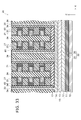
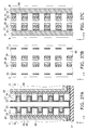
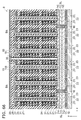
- FIG. 1 is a perspective view showing a semiconductor memory device according to a first embodiment
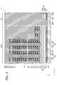
- FIG. 2 is a cross-sectional view showing the semiconductor memory device according to the first embodiment
- FIG. 3 is a cross-sectional view showing region A shown in FIG. 2
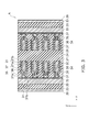
- FIG. 4 is a cross-sectional view along line B-B' shown in FIG. 2
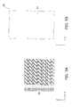
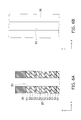
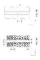
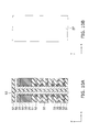
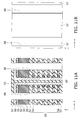
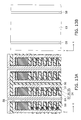
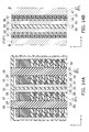
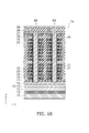
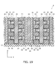
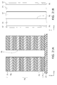
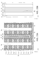
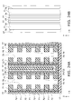
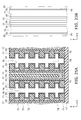
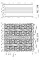
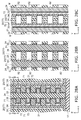
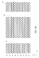
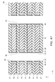
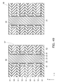
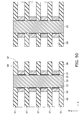
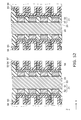
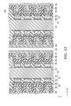
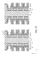
- FIG. 5A to FIG. 17B are plan views and cross-sectional views showing a method for manufacturing the semiconductor memory device according to the first embodiment
- FIG. 18 is a cross-sectional view showing a semiconductor memory device according to a modification of the first embodiment
- FIG. 19 is a cross-sectional view showing a semiconductor memory device according to a second embodiment
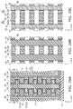
- FIGS. 30C are plan views and cross-sectional views showing a method for manufacturing the semiconductor memory device according to the second embodiment
- FIG. 31 is a cross-sectional view showing a semiconductor memory device according to a first modification of the second embodiment
- FIG. 32 is a cross-sectional view showing a semiconductor memory device according to a second modification of the second embodiment
- FIG. 33 is a cross-sectional view showing a semiconductor memory device according to a third modification of the second embodiment
- FIG. 34 is a cross-sectional view showing a semiconductor memory device according to a third embodiment
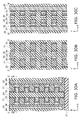
- FIGS. 35A to 37C are plan views and cross-sectional views showing the method for manufacturing the semiconductor memory device according to the third embodiment
- FIGS. 35A to 37C are plan views and cross-sectional views showing the method for manufacturing the semiconductor memory device according to the third embodiment
- FIGS. 35A to 37C are plan views and cross-sectional views showing the method for manufacturing the semiconductor memory device according to the third embodiment
- FIGS. 35A to 37C are plan views and
- FIGS. 39A to 39C are cross-sectional views showing a method for manufacturing the semiconductor memory device according to the modification of the third embodiment
- FIG. 40 is a cross-sectional view showing a semiconductor memory device according to a forth embodiment
- FIG. 41 is a cross-sectional view showing region E shown in FIG. 40
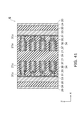
- FIG. 42A is a cross-sectional view showing a method for manufacturing the semiconductor memory device according to the forth embodiment
- FIG. 42B is a plan view
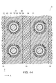
- FIG. 43 and FIG. 44 are cross-sectional views showing a semiconductor memory device according to a fifth embodiment
- FIG. 53 are cross-sectional views showing a method for manufacturing the semiconductor memory device according to the fifth embodiment
- FIG. 54 is a cross-sectional view showing a semiconductor memory device according to a modification of the fifth embodiment
- FIG. 55 to FIG. 57 are cross-sectional views showing the method for manufacturing the semiconductor memory device according to the modification of the fifth embodiment
- FIG. 58 to FIG. 59 are cross-sectional views showing a semiconductor memory device according to a sixth embodiment
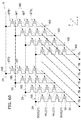
- FIG. 60 is a schematic circuit diagram showing the semiconductor memory device according to the sixth embodiment
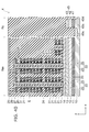
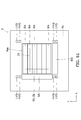
- FIG. 61 is a schematic plan view showing the semiconductor memory device according to the sixth embodiment
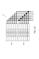
- FIG. 62 shows connection relationship of the cell source lines in the semiconductor memory device according to the sixth embodiment
- FIG. 64 is a cross-sectional view showing a semiconductor memory device according to a seventh embodiment
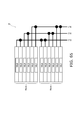
- FIG. 65 shows connection relationship of the cell source lines in the semiconductor memory device according to the seventh embodiment
- FIG. 66 is a cross-sectional view showing a semiconductor memory device according to an eighth embodiment
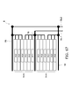
- FIG. 67 shows connection relationship of the cell source lines in the semiconductor memory device according to the eighth embodiment
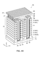
- FIG. 68 is a perspective view showing a semiconductor memory device according to a ninth embodiment
- FIG. 69 is a perspective view showing a semiconductor memory device according to a tenth embodiment.
- a semiconductor memory device in general, includes a substrate, a semiconductor pillar provided on the substrate to extend in a vertical direction, a plurality of first electrode films provided sideward of the semiconductor pillar to extend in a first direction. The plurality of first electrode films are disposed to be separated from each other along the vertical direction.
- the semiconductor memory device further includes a plurality of second electrode films provided between the semiconductor pillar and the first electrode films. The plurality of second electrode films are disposed to be separated from each other along the vertical direction.
- the semiconductor memory device further includes a first insulating film provided between the semiconductor pillar and the second electrode films, and a second insulating film provided between the second electrode film and the first electrode film.
- FIG. 1 is a perspective view showing a semiconductor memory device according to the embodiment.
- FIG. 2 is a cross-sectional view showing the semiconductor memory device according to the embodiment.
- FIG. 3 is a cross-sectional view showing region A shown in FIG. 2.
- FIG. 4 is a cross-sectional view along line B-B' shown in FIG. 2.
- a silicon substrate 10 is provided in the semiconductor memory device 1 according to the embodiment.
- a memory cell region Rm and a peripheral circuit region Rc are set in the silicon substrate 10.
- an XYZ orthogonal coordinate system is employed in the specification for convenience of description. Two mutually-orthogonal directions parallel to an upper surface 10a of the silicon substrate 10 are taken as an X-direction and a Y-direction; and a direction perpendicular to the upper surface 10a is taken as a Z-direction.
- an insulating film 11 (a third insulating film) that is made of, for example, silicon oxide, a conductive layer 12 that is made of, for example, polysilicon, an interconnect layer 13 that is made of, for example, tungsten, and a conductive layer 14 that is made of, for example, polysilicon are stacked in this order on the silicon substrate 10.
- a cell source line 15 is formed of the conductive layer 12, the interconnect layer 13, and the conductive layer 14.
- An insulating film 17 that is made of, for example, silicon oxide is provided on the cell source line 15.
- Multiple silicon pillars 20 that extend in the Z-direction are provided on the cell source line 15.
- the silicon pillars 20 are made of, for example, polysilicon; and the lower ends of the silicon pillars 20 pierce the insulating film 17 to be connected to the cell source line 15.
- the silicon pillars 20 are arranged in a matrix configuration along the X-direction and the Y-direction as viewed from the Z-direction and have a common connection with a single cell source line 15.
- control gate electrode films (the first electrode films) 21 are provided sideward of the silicon pillar 20 to be separated from each other along the Z-direction.
- Each of the control gate electrode films 21 is made of, for example, tungsten and extends in the Y-direction. Therefore, the control gate electrode films 21 are not disposed between the silicon pillars 20 arranged along the Y-direction. Also, in the X-direction, two of the silicon pillars 20 are arranged alternately with two of the control gate electrode films 21.
- the silicon pillars 20 arranged along the X-direction are organized into multiple sets 22 every two mutually-adjacent silicon pillars 20 and when two of the control gate electrode films 21 are arranged to be positioned between the sets 22, the control gate electrode films 21 are not disposed between the two silicon pillars 20 belonging to each set 22.
- An inter-layer insulating film 23 is provided between the silicon pillars 20.
- An inter-layer insulating film 24 that is made of, for example, silicon oxide is provided between the control gate electrode films 21, below the control gate electrode film 21 of the lowermost layer, and above the control gate electrode film 21 of the uppermost layer.
- a hard mask 26 is provided on a stacked body 25 that is made of the multiple control gate electrode films 21, the inter-layer insulating film 23, and the inter-layer insulating film 24.
- the silicon pillar 20 is drawn out onto the hard mask 26 to be a single body with an interconnect 27 extending in the X-direction.
- a via 28 is provided on the interconnect 27; and a bit line 29 that extends in the X-direction is provided on the via 28.
- the bit line 29 is connected to the interconnect 27 by the via 28.
- each of the silicon pillars 20 is connected between the bit line 29 and the cell source line 15.
- the semiconductor memory device 1 is an I-shaped pillar type stacked memory device.
- the Y-direction end portion of the stacked body 25 is patterned into a stairstep configuration; and at the end portion of the stairstep configuration, the multiple control gate electrode films 21 that have the same position in the Z-direction are bundled together.
- a via 38 is provided on the end portion of the bundled control gate electrode films 21.
- a word line 39 that extends in the Y-direction is provided on the via 38. In the Z-direction, the position of the word line 39 is the same as the position of the bit line 29.
- the word line 39 is connected to the control gate electrode film 21 by the via 38.
- floating gate electrode films 31 (second electrode films) that are made of, for example, polysilicon are provided between the silicon pillars 20 and the control gate electrode films 21. Because the floating gate electrode films 31 are provided at each intersection between the silicon pillars 20 and the control gate electrode films 21, the floating gate electrode films 31 are arranged in a matrix configuration to be separated from each other along the Y-direction and the Z-direction. As described above, because the silicon pillars 20 and the control gate electrode films 21 are arranged along the X-direction, the floating gate electrode films 31 are also arranged along the X-direction. AS a result, the floating gate electrode films 31 are arranged in the XYZ three-dimensional matrix configuration.
- the configuration of the floating gate electrode film 31 is a fan-like shape that is wider on the control gate electrode film 21 side. Therefore, a length L1 in the Y-direction of the end portion of the floating gate electrode film 31 on the silicon pillar 20 side is shorter than a length L2 in the Y-direction of the end portion of the floating gate electrode film 31 on the control gate electrode film 21 side.
- a tunneling insulating film 33 that is made of, for example, silicon oxide is provided between the silicon pillar 20 and the floating gate electrode films 31.
- the tunneling insulating film 33 is provided at each silicon pillar 20; and the configuration of the tunneling insulating film 33 is a band configuration that extends in the Z-direction and has the X-direction as the thickness direction and the Y-direction as the width direction.
- a blocking insulating film 34 is provided between the floating gate electrode film 31 and the control gate electrode film 21.
- the blocking insulating film 34 is, for example, a three-layer film in which a silicon nitride layer 35, a silicon oxide layer 36, and a silicon nitride layer 37 are stacked in this order from the floating gate electrode film 31 side toward the control gate electrode film 21 side.
- the silicon nitride layer 35 is formed around the floating gate electrode film 31 to cover an upper surface 31a and a lower surface 31b of the floating gate electrode film 31.
- the silicon oxide layer 36 and the silicon nitride layer 37 are formed around the control gate electrode film 21 to cover an upper surface 21a and a lower surface 21b of the control gate electrode film 21.
- the tunneling insulating film 33 normally is insulative
- the tunneling insulating film 33 is a film in which a tunneling current flows when a voltage within the range of the drive voltage of the semiconductor memory device 1 is applied.
- the blocking insulating film 34 is a film in which a current substantially does not flow even when a voltage within the range of the drive voltage of the semiconductor memory device 1 is applied.
- the equivalent oxide thickness (EOT) of the tunneling insulating film 33 is thicker than the equivalent oxide thickness of the blocking insulating film 34; and the dielectric constant of the tunneling insulating film 33 is lower than the dielectric constant of the blocking insulating film.
- a source region 40s and a drain region 40d are formed in the silicon substrate 10 to be separated from each other.
- the region between the source region 40s and the drain region 40d is a channel region 40c.
- a gate insulating film 41 (a fourth insulating film) that is made of, for example, silicon oxide is provided on the silicon substrate 10 in the region directly above the channel region 40c; and a conductive layer 42 that is made of, for example, polysilicon and an interconnect layer 43 that is made of, for example, tungsten are stacked in this order on the gate insulating film 41.
- a gate electrode 45 is formed of the conductive layer 42 and the interconnect layer 43.
- a transistor 46 includes the source region 40s, the drain region 40d, the channel region 40c, the gate insulating film 41, and the gate electrode 45. The transistor 46 is included in the peripheral circuit.
- the insulating film 11 that is in the memory cell region Rm and the gate insulating film 41 that is in the peripheral circuit region Rc are formed by dividing the same silicon oxide film; the conductive layer 12 that is in the memory cell region Rm and the conductive layer 42 that is in the peripheral circuit region Rc are formed by dividing the same polysilicon layer; and the interconnect layer 13 that is in the memory cell region Rm and the interconnect layer 43 that is in the peripheral circuit region Rc are formed by dividing the same tungsten layer.
- FIG. 5A to FIG. 17B are plan views and cross-sectional views showing the method for manufacturing the semiconductor memory device according to the embodiment. Only the memory cell region Rm is shown in FIG. 5A to FIG. 17B.
- the channel region 40c, the source region 40s, and the drain region 40d are formed in the upper layer portion of the silicon substrate 10 in the peripheral circuit region Rc. Then, a silicon oxide film is formed on the silicon substrate 10 in both the memory cell region Rm and the peripheral circuit region Rc. Therefore, in the peripheral circuit region Rc, a relatively thin silicon oxide film is formed in the low breakdown voltage transistor (LV Tr) region; and a relatively thick silicon oxide film is formed in the high breakdown voltage transistor (HV Tr) region. Also, a relatively thick silicon oxide film is formed in the memory cell region Rm.
- LV Tr low breakdown voltage transistor
- HV Tr high breakdown voltage transistor
- a polysilicon layer is formed on the entire surface.
- STI Shallow Trench Isolation
- a tungsten layer is formed in the upper layer portion of the silicon substrate 10 in the peripheral circuit region Rc using an appropriate mask (not shown).
- a tungsten layer is formed in the upper layer portion of the silicon substrate 10 in the peripheral circuit region Rc using an appropriate mask (not shown).
- a tungsten layer is formed in the upper layer portion of the silicon substrate 10 in the peripheral circuit region Rc using an appropriate mask (not shown).
- a tungsten layer is formed.
- a polysilicon layer and a silicon oxide film are formed only in the memory cell region Rm.
- these layers are patterned by RIE (Reactive Ion Etching).
- the insulating film 11, the conductive layer 12, the interconnect layer 13, the conductive layer 14, and the insulating film 17 are formed for each block in the memory cell region Rm.
- the cell source line 15 is formed of the stacked body made of the conductive layer 12, the interconnect layer 13, and the conductive layer 14. Erasing is possible by block unit by forming the cell source line 15 to be divided for each block.
- the gate insulating film 41, the conductive layer 42, and the interconnect layer 43 are formed in the peripheral circuit region Rc.
- the gate electrode 45 is formed of the stacked body made of the conductive layer 42 and the interconnect layer 43. Thereby, the transistor 46 is formed in the peripheral circuit region Rc.
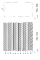
- FIGS. 5A and 5B a silicon oxide film 51 and a silicon nitride film 52 are stacked alternately on the insulating film 17 (referring to FIG. 2) in the memory cell region Rm. Thereby, the stacked body 25 is formed.
- the gate length (the total thickness of the control gate electrode film 21 and the blocking insulating film provided around the control gate electrode film 21) on the electrode side is longer than the gate length (the total thickness of the floating gate electrode film 31 and the blocking insulating film provided around the floating gate electrode film 31) on the channel side
- the film thickness ratio of the silicon oxide film 51 and the silicon nitride film 52 that are stacked is adjusted according to the film thickness of the blocking films filled from both sides.
- FIG. 5A is a cross-sectional view; and FIG. 5B is a top view. This is similar for the following drawings as well.
- the hard mask 26 that is made of, for example, silicon nitride is formed on the stacked body 25. Then, the hard mask 26 is patterned; and anisotropic etching such as RIE, etc., of the stacked body 25 is performed using the patterned hard mask 26 as a mask. Thereby, multiple trenches 53 are made in the stacked body 25 to extend in the Y-direction. The trenches 53 pierce the stacked body 25.
- the silicon nitride films 52 are recessed by performing wet etching via the trench 53. Thereby, the exposed surfaces of the silicon nitride films 52 recede at the inner surface of the trench 53 to make recesses 54 that extend in the Y-direction. Then, oxidation treatment is performed by SPA, etc. Thereby, the exposed surfaces of the silicon nitride films 52 at the inner surface of the trench 53 are covered with a thin silicon oxide layer 50.
- the silicon nitride layer 35 is formed on the entire surface. Then, a polysilicon film 55 is formed on the entire surface. The silicon nitride layer 35 and the polysilicon film 55 also are formed on the inner surface of the trench 53 to enter the recesses 54.
- the polysilicon film 55 and the silicon nitride layer 35 are selectively removed to remain inside the recesses 54; and the polysilicon films 55 that remain inside the recesses 54 adjacent to each other in the Z-direction are separated from each other.
- the silicon nitride layers 35 that remain inside the recesses 54 adjacent to each other in the Z-direction also are separated from each other.
- the tunneling insulating film 33, a polysilicon film 56, and an insulating film 57 are deposited in this order.
- trenches 58 are made in the stacked body 25 and the stacked body stacked above the stacked body 25 to extend in the Y-direction between the trenches 53. Thereby, the trenches 53 and the trenches 58 are arranged alternately along the X-direction.
- the silicon nitride films 52 are recessed by performing wet etching using hot phosphoric acid via the trench 58.
- the recessing is stopped by the silicon oxide layer 50 that is exposed at the back surfaces of recesses 59.
- the silicon nitride films 52 are removed; and the recesses 59 are made in the inner surface of the trench 58 to extend in the Y-direction.
- the silicon nitride layer 35 is not damaged because the silicon nitride layer 35 is protected by the silicon oxide layer 50.
- the silicon oxide layer 50 that is exposed at the back surfaces of the recesses 59 is removed. Thereby, the silicon nitride layers 35 are exposed at the back surfaces of the recesses 59. Then, the silicon oxide layer 36 and the silicon nitride layer 37 are formed on the inner surface of the trench 58. As a result, as shown in FIG. 3, the blocking insulating film 34 is formed of the silicon nitride layer 35, the silicon oxide layer 36, and the silicon nitride layer 37. Then, a tungsten film 61 is formed on the entire surface by, for example, CVD (Chemical Vapor Deposition). The silicon oxide layer 36, the silicon nitride layer 37, and the tungsten film 61 also enter the recesses 59 via the trench 58.
- CVD Chemical Vapor Deposition
- the tungsten film 61 is selectively removed by performing anisotropic etching such as RIE, etc. Thereby, the tungsten film 61 is caused to remain inside the recesses 59; and the tungsten films 61 that remain inside the recesses 59 adjacent to each other in the Z-direction are separated from each other. As a result, the control gate electrode films 21 that are made of the tungsten films 61 are formed inside the recesses 59. Subsequently, the inter-layer insulating film 24 is filled into the trench 58; and the upper surface of the inter-layer insulating film 24 is planarized.
- FIG. 14B is a cross-sectional view along line B-B' shown in FIG. 14A.
- a hard mask 62 is formed in which openings 62a are arranged in a matrix configuration along the X-direction and the Y-direction.
- the configuration of each of the openings 62a is a rectangle with the X-direction as the longitudinal direction; and the openings 62a are arranged intermittently along the Y-direction in the region directly above the polysilicon films 56 and the insulating film 57 between the polysilicon films 56 but are not disposed in the region directly above the inter-layer insulating film 24.
- FIG. 15B is a plan view along line C-C' shown in FIG. 15A; and FIG. 15C is a cross-sectional view along line B-B' shown in FIG. 15A.
- the tunneling insulating film 33 and the polysilicon films 55 are selectively removed by performing isotropic etching such as CDE (Chemical Dry Etching), wet etching, etc., via the through-hole 63. Thereby, the tunneling insulating film 33 and the polysilicon films 55 are divided along the Y-direction. The insulating film 57 (see FIG. 15A) also is removed. As a result, the floating gate electrode films 31 are formed of the polysilicon films 55.
- isotropic etching such as CDE (Chemical Dry Etching), wet etching, etc.
- the length L1 in the Y-direction of the end portion of the floating gate electrode film 31 on the silicon pillar 20 side is shorter than the length L2 in the Y-direction of the end portion of the floating gate electrode film 31 on the control gate electrode film 21 side.
- the inter-layer insulating film 24 remains without being removed.
- the inter-layer insulating film 23 is deposited on the entire surface.
- the inter-layer insulating film 23 is filled also inside the through-hole 63.
- the silicon oxide film 51 also becomes a portion of the inter-layer insulating film 23.
- the vias 28, the vias 38, the bit lines 29, and the word lines 39 are formed.
- the semiconductor memory device 1 according to the embodiment is manufactured.
- the floating gate electrode films 31 that are made of polysilicon are provided as charge storage units. Therefore, the data retention characteristics of the memory cells are good; and the erasing operation is fast because the charge that is stored in the floating gate electrode films 31 can be erased by moving electrons instead of holes. The data retention characteristics are even better because the floating gate electrode films 31 are separated from each other.
- the blocking insulating film 34 is a three-layer film made of the silicon nitride layer 35, the silicon oxide layer 36, and the silicon nitride layer 37, the coupling ratio can be ensured while suppressing the leakage current.
- the silicon nitride layer 35 is formed from the silicon pillar 20 side in the process shown in FIGS. 8A and 8B; and the silicon oxide layer 36 and the silicon nitride layer 37 are formed from the control gate electrode film 21 side in the process shown in FIGS. 13A and 13B.
- the thickness of the blocking insulating film 34 can be distributed on the two X-direction sides of the floating gate electrode film 31; and the thickness in the Z-direction as an entirety can be reduced.
- the height in the Z-direction of the recesses 54 (referring to FIGS. 8A and 8B) and the recesses 59 (referring to FIGS. 13A and 13B) can be reduced; the bit density of the memory cells in the Z-direction can be increased; and the aspect ratio can be reduced.
- the blocking insulating film 34 is divided for each of the control gate electrode films 21 along the Z-direction. Thereby, the electrons that are stored in the floating gate electrode film 31 can be prevented from propagating through the blocking insulating film 34 and leaking. As a result, the data retention characteristics of the memory cells are good.
- the configuration of the floating gate electrode film 31 is a fan-like shape that is wider on the control gate electrode film 21 side.
- the IPD capacitance between the floating gate electrode film 31 and the control gate electrode film 21 can be large; and the coupling ratio can be large.
- the blocking insulating film 34 is a three-layer film, this is not limited thereto.
- the layers of the blocking insulating film 34 are not limited to the silicon oxide layer (the SiO 2 layer) and the silicon nitride layers (the Si 3 N 4 layers) and may be a high dielectric constant layer such as, for example, an Al 2 O 3 layer, a MgO layer, a SrO layer, a SiN layer, a BaO layer, a TiO layer, a Ta 2 O 5 layer, a BaTiO 3 layer, a BaZrO layer, a ZrO 2 layer, a Y 2 O 3 layer, a ZrSiO layer, a HfAlO layer, a HfSiO layer, a La 2 O 3 layer, a LaAlO layer, etc.
- the floating gate electrode film 31 is not limited thereto and may be formed of, for example, a metal silicide or a metal.
- control gate electrode film 21 is formed of tungsten
- the control gate electrode film 21 is not limited thereto and may be formed of, for example, a metal silicide by filling a polysilicon film and subsequently siliciding the polysilicon film.
- the silicon nitride films 52 of the lowermost layer and the uppermost layer may be formed to be thicker than the other silicon nitride films 52.
- the film thicknesses of the selection gate electrode films that are formed below and above the control gate electrode films 21 can be thicker than those of the control gate electrode films 21.
- a selection transistor that has a gate length longer than that of the memory cell transistor can be formed.
- control gate electrode films 21 provided at the upper portion of the stacked body 25 may be shorted to each other to be used as the selection gate electrode film; and several layers of the control gate electrode films 21 provided at the lower portion of the stacked body 25 may be shorted to each other to be used as the selection gate electrode film.
- a selection transistor that has a gate length longer than that of the memory cell transistor can be formed.
- FIG. 18 is a cross-sectional view showing a semiconductor memory device according to the modification.
- one wide silicon pillar 65 is provided between two floating gate electrode films 31 adjacent to each other in the X-direction.
- the inter-layer insulating film 24 is not provided between the two silicon pillars 20 belonging to each of the sets 22; and the two silicon pillars 20 are formed as one body.
- the two X-direction side portions of the wide silicon pillar 65 are used as distinct channels. Otherwise, the configuration, the manufacturing method, and the effects of the modification are similar to those of the first embodiment described above.
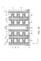
- FIG. 19 is a cross-sectional view showing a semiconductor memory device according to the embodiment.
- the semiconductor memory device 2 differs from the semiconductor memory device 1 (referring to FIG. 1 to FIG. 4) according to the first embodiment described above in that the disposition of the tunneling insulating film 33 and the blocking insulating film 34 is reversed.
- the blocking insulating film 34 is disposed between the silicon pillar 20 and the floating gate electrode films 31; and the tunneling insulating film 33 is disposed between the floating gate electrode films 31 and the control gate electrode films 21. Therefore, the components included in the memory cell are arranged in the order of silicon pillar 20-blocking insulating film 34-floating gate electrode film 31-tunneling insulating film 33-control gate electrode film 21.
- silicon oxide films 71 are arranged to be separated from each other along the Z-direction; and the floating gate electrode films 31 and the control gate electrode films 21 are provided in the spaces between the mutually-adjacent silicon oxide films 71.
- the tunneling insulating film 33 is disposed to cover the upper surface and the lower surface of the control gate electrode film 21 and the side surface of the control gate electrode film 31 on the floating gate electrode film 31 side.
- the blocking insulating film 34 is disposed linearly along the side surface of the silicon pillar 20.
- the blocking insulating film 34 may be a multilayered film, e.g., a three-layer film. However, the blocking insulating film 34 is not subdivided between the silicon pillar 20 side and the control gate electrode film 21 side; and the entire blocking insulating film 34 is disposed on the silicon pillar 20 side.
- the semiconductor memory device 2 the lower end portions of the two silicon pillars 20 belonging to the set 22 are connected to each other; and the cell source line 15 is not provided.
- a source line (not shown) is provided above the stacked body.
- the semiconductor memory device 2 is a U-shaped pillar type stacked memory device. Otherwise, the configuration of the embodiment is similar to that of the first embodiment described above.
- the basic operations and the read-out method of the semiconductor memory device 2 are similar to those of a normal NAND flash memory; and the polarity of the voltage applied between the silicon pillar 20 and the control gate electrode film 21 in the programming operation and the erasing operation are the reverse of those of a normal NAND flash memory. Thereby, the charge is caused to move into and out of the silicon pillar 20 from the control gate electrode film 21.
- FIG. 20A to FIG. 30C are plan views and cross-sectional views showing the method for manufacturing the semiconductor memory device according to the embodiment.
- the insulating film 17 that is made of silicon oxide is formed on the silicon substrate 10 (referring to FIG. 2); and subsequently, a stacked body 73 is formed by alternately stacking the silicon oxide film 71 and a polysilicon film 72.
- the polysilicon film 72 may be doped with boron (B), may be doped with phosphorus (P), or may not be doped.
- FIG. 20A is a cross-sectional view; and FIG. 20B is a top view. This is similar for the following drawings as well.
- multiple trenches 75 are made in the stacked body 73 to extend in the Y-direction by forming a hard mask (not shown) on the stacked body 73, patterning by lithography, and performing anisotropic etching such as RIE, etc., using the patterned hard mask as a mask.
- the trenches 75 pierce the stacked body 73 in the Z-direction but do not pierce the insulating film 17.
- the blocking insulating film 34 is formed; and subsequently, a polysilicon film 77 is formed.
- the blocking insulating film 34 and the polysilicon film 77 are formed on the side surface of the trench 75 and on the bottom surface of the trench 75 to be folded back into a U-shaped as viewed from the Y-direction. Accordingly, the relationship between the width of the trench 75 and the film thicknesses of the blocking insulating film 34 and the polysilicon film 77 is set such that such folding back is possible.
- the inter-layer insulating film 24 is filled into the trench 75 by depositing silicon oxide.
- trenches 78 are made in the portion of the stacked body 73 between the trenches 75 to extend in the Y-direction by forming a hard mask (not shown) on the stacked body 73, patterning by lithography, and performing anisotropic etching such as RIE, etc., using the patterned hard mask as a mask.
- the trenches 75 and the trenches 78 are arranged alternately along the X-direction.
- wet etching is performed using, for example, TMY (choline aqueous solution).
- TMY choline aqueous solution
- the polysilicon films 72 are etched isotropically via the trench 78; and the exposed surfaces of the polysilicon films 72 at the inner surface of the trench 78 are caused to recede.
- recesses 79 are made at the inner surface of the trench 78.
- the tunneling insulating film 33 is formed by depositing silicon oxide on the inner surface of the trench 78. At this time, the tunneling insulating film 33 is formed also on the inner surfaces of the recesses 79 to contact the polysilicon films 72.
- the tunneling insulating film 33 may be formed by thermal oxidation of the exposed surfaces of the polysilicon films 72.
- a tungsten film 81 is formed inside the trench 78 by, for example, depositing tungsten by CVD. At this time, the tungsten film 81 is filled also into the recesses 79.
- the portion of the tungsten film 81 that is not filled into the recesses 79 is removed by etching the tungsten film 81. Thereby, the tungsten films 81 that remain inside the recesses 79 are separated from each other between the recesses 79 to become the control gate electrode films 21. Then, the inter-layer insulating film 24 is filled into the trench 78; and the upper surface of the inter-layer insulating film 24 is planarized.
- silicon may be deposited in the process shown in FIGS. 26A and 26B; and the silicon may be silicided in this process. Thereby, the control gate electrode films 21 are formed of a metal silicide.
- FIGS. 28A to 28C through-holes 82 are made in the trench 75 by selectively removing the inter-layer insulating film 24, the polysilicon film 77, and the blocking insulating film 34 by performing anisotropic etching using an appropriate mask.
- the polysilicon film 77 is divided periodically along the Y-direction by the through-holes 82 to become the silicon pillars 20.
- FIG. 28A is a cross-sectional view
- FIG. 28B is a cross-sectional view along line C-C' shown in FIG. 28A
- FIG. 28C is a cross-sectional view along line B-B' shown in FIG. 28A. This is similar for FIGS. 29A to 29C and FIGS. 30A to 30C.
- the blocking insulating film 34, the polysilicon films 72, and the tunneling insulating film 33 are further removed via the through-holes 82 to be divided along the Y-direction by performing isotropic etching such as CDE, wet etching, etc.
- isotropic etching such as CDE, wet etching, etc.
- the polysilicon films 72 that are divided along the Y-direction become the floating gate electrode films 31.
- the configuration of the floating gate electrode film 31 becomes a fan-like shape that is wider on the control gate electrode film 21 side according to the conditions of the isotropic etching.
- the inter-layer insulating film 24 is filled into the through-holes 82 by, for example, depositing silicon oxide and planarizing the upper surface of the silicon oxide. Then, the vias 28, the vias 38, the source lines, the bit lines 29, and the word lines 39 (referring to FIG. 1 and FIG. 2) are formed by normal methods. Thus, the semiconductor memory device 2 according to the embodiment is manufactured.
- the thickness of the control gate electrode film 21, which is covered with the blocking insulating film 34 at the upper surface and the lower surface of the control gate electrode film 21, becomes shorter than the spacing of the silicon oxide films 71. Accordingly, the interconnect resistance of the control gate electrode film 21 increases; the gate length of the memory cell transistor becomes short; and the characteristics of the memory cell transistor undesirably degrade due to the short channel effect.
- the blocking insulating film 34 is formed on the inner surface of the trench 75 in the process shown in FIGS. 22A and 22B.
- the blocking insulating film 34 is formed at an early stage, it is no longer necessary for the blocking insulating film 34 to extend around into the gaps between the silicon oxide films 71; and the spacing of the silicon oxide films 71 can be shorter.
- the tunneling insulating film 33 extends around into the gaps between the silicon oxide films 71, there are few problems because the tunneling insulating film 33 is thinner than the blocking insulating film 34 as described above.
- the bit density of the memory cells in the Z-direction can be increased after ensuring the thickness of the control gate electrode film 21; and the aspect ratio can be reduced. Otherwise, the effects of the embodiment are similar to those of the first embodiment described above.
- FIG. 31 is a cross-sectional view showing a semiconductor memory device according to the modification.
- a charge storage film 85 that is made of an insulative charge storage material is provided instead of the floating gate electrode film 31 that is made of a conductive material.
- the charge storage film 85 is formed of, for example, silicon nitride. Accordingly, the memory cell of the semiconductor memory device 2a has a MONOS structure. Otherwise, the configuration, the manufacturing method, the operations, and the effects of the modification are similar to those of the second embodiment described above.
- FIG. 32 is a cross-sectional view showing a semiconductor memory device according to the modification.
- the cell source line 15 is provided; and the lower end of the silicon pillar 20 is connected to the cell source line 15.
- the semiconductor memory device 2b is an I-shaped pillar type stacked memory device.
- the portion of the blocking insulating film 34 formed on the bottom surface of the trench 75 is removed by etching in the process shown in FIGS. 22A and 22B.
- the etching does not damage the tunneling insulating film 33 because the tunneling insulating film 33 is not yet formed at this time. Otherwise, the configuration, the manufacturing method, the operations, and the effects of the modification are similar to those of the second embodiment described above.
- FIG. 33 is a cross-sectional view showing a semiconductor memory device according to the modification.
- the modification is an example in which the first modification and the second modification described above are combined.
- the charge storage film 85 that is made of an insulative charge storage material is provided; and the lower end of the silicon pillar 20 is connected to the cell source line 15.
- the semiconductor memory device 2c has a MONOS structure and is the I-shaped pillar type. Otherwise, the configuration, the manufacturing method, the operations, and the effects of the modification are similar to those of the second embodiment and the first and second modifications of the second embodiment described above.
- FIG. 34 is a cross-sectional view showing a semiconductor memory device according to the embodiment.
- an air gap 86 is made between the silicon pillars 20, the control gate electrode films 21, the floating gate electrode films 31, the tunneling insulating films 33, and the blocking insulating films 34.
- the air gap 86 is made between the control gate electrode films 21 adjacent to each other in the Z-direction, between the floating gate electrode films 31 adjacent to each other in the Z-direction, between the silicon pillars 20 adjacent to each other in the Y-direction, between the blocking insulating films 34, between the floating gate electrode films 31, between the tunneling insulating films 33, and between the two silicon pillars 20 adjacent to each other in the X-direction and belonging to the same set 22.
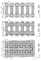
- FIGS. 35A and 35B to FIGS. 37A to 37C are plan views and cross-sectional views showing the method for manufacturing the semiconductor memory device according to the embodiment.
- FIG. 35A is a cross-sectional view
- FIG. 35B is a plan view.
- FIG. 36A is a cross-sectional view
- FIG. 36B is a cross-sectional view along line C-C' shown in FIG. 36A
- FIG. 36C is a cross-sectional view along line B-B' shown in FIG. 36A. This is similar for FIGS. 37A to 37C.
- a stacked body is formed by forming the insulating film 17 made of silicon oxide on the silicon substrate 10 (referring to FIG. 2) and subsequently stacking a silicon nitride film 87 alternately with the polysilicon film 72.
- FIGS. 21A and 21B to FIGS. 29A to 29C are implemented.
- a silicon nitride film 88 is filled instead of the inter-layer insulating film 24 made of silicon oxide.
- FIGS. 36A to 36C an intermediate structural body that is similar to the intermediate structural body shown in FIGS. 29A to 29C is made.
- the silicon nitride films 87 are provided instead of the silicon oxide films 71; and the silicon nitride film 88 is provided instead of the inter-layer insulating film 24.
- the silicon nitride films 87 and the silicon nitride film 88 are removed by, for example, wet etching. Thereby, the air gap 86 is made in the space where the silicon nitride films 87 and the silicon nitride film 88 were disposed.
- the semiconductor memory device 3 according to the embodiment is manufactured.
- the air gap 86 is made between the silicon pillars 20, the control gate electrode films 21, the floating gate electrode films 31, the tunneling insulating films 33, and the blocking insulating films 34, the proximity effect can be suppressed; and the breakdown voltage can be increased.
- the air gap is made only between the silicon pillars 20 by alternately stacking the silicon oxide film 71 and the polysilicon film 72 instead of the silicon nitride film 87 and the polysilicon film 72 in the process shown in FIGS. 35A and 35B.
- FIGS. 38A to 38C are cross-sectional views showing a semiconductor memory device according to the modification.
- FIG. 38A is a cross-sectional view
- FIG. 38B is a cross-sectional view along line C-C' shown in FIG. 38A
- FIG. 38C is a cross-sectional view along line B-B' shown in FIG. 38A.
- FIG. 38A is a cross-sectional view along line D-D' shown in FIG. 38C. This is similar for FIGS. 39A to 39C described below.
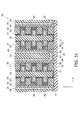
- the semiconductor memory device 3a according to the modification differs from the semiconductor memory device 3 (referring to FIG. 34) according to the third embodiment described above in that a reinforcing member 89 is formed in multiple regions by causing the silicon nitride films 87 and 88 to partially remain.
- the reinforcing member 89 extends in the Z-direction and is disposed intermittently along the Y-direction inside the semiconductor memory device 3a.
- FIGS. 39A to 39C are cross-sectional views showing a method for manufacturing the semiconductor memory device according to the modification.
- the through-holes 82 are not made in the region where the reinforcing member 89 is to be formed. Thereby, in the process shown in FIGS. 37A to 37C, the silicon nitride films 87 and 88 remain locally to become the reinforcing member 89 when performing wet etching of the silicon nitride films 87 and 88 via the through-holes 82.
- the reinforcing member 89 by providing the reinforcing member 89, the mechanical strength of the semiconductor memory device 3a can be ensured; and collapse can be prevented. Otherwise, the configuration, the manufacturing method, the operations, and the effects of the modification are similar to those of the third embodiment described above.
- FIG. 40 is a cross-sectional view showing a semiconductor memory device according to the embodiment.
- FIG. 41 is a cross-sectional view showing region E shown in FIG. 40.
- the semiconductor memory device 4 according to the embodiment differs from the semiconductor memory device 1 (referring to FIG. 1 to FIG. 4) according to the first embodiment described above in that the blocking insulating film 34 is not disposed between a control gate electrode film 21u of the uppermost level and a floating gate electrode film 31u of the uppermost level; and the control gate electrode film 21u of the uppermost level is connected to the floating gate electrode film 31u of the uppermost level.
- FIG. 42A is a cross-sectional view showing a method for manufacturing the semiconductor memory device according to the embodiment.
- FIG. 42B is a plan view.
- FIGS. 5A and 5B to FIGS. 12A and 12B are implemented.
- the silicon oxide layer 36 and the silicon nitride layer 37 are formed on the inner surface of the trench 58.
- a resist material 90 is filled into the trench 58; and a recess 59u of the uppermost level is exposed by the upper surface of the resist material 90 being recessed.
- the portions of the silicon nitride layer 37, the silicon oxide layer 36, and the silicon nitride layer 35 that are exposed from the resist material 90 are removed by, for example, wet etching. Thereby, the polysilicon film 55 is exposed at the back surface of the recess 59u of the uppermost level. Then, the resist material 90 is removed.
- the tungsten film 61 is formed on the inner surface of the trench 58. At this time, the tungsten film 61 contacts the polysilicon film 55 inside the recess 59u of the uppermost level.
- the subsequent processes are similar to those of the first embodiment described above.
- control gate electrode film 21u of the uppermost level and the floating gate electrode film 31u of the uppermost level can be electrically integrated to be used as the selection gate electrode film by causing the control gate electrode film 21u to connect the floating gate electrode film 31u.
- a selection gate transistor can be formed in which the threshold does not fluctuate because charge is not stored.
- FIG. 43 and FIG. 44 are cross-sectional views showing a semiconductor memory device according to the embodiment.
- the multiple silicon pillars 20 are provided and arranged in a matrix configuration along the X-direction and the Y-direction.
- Each of the silicon pillars 20 has a circular columnar configuration extending in the Z-direction.
- the tunneling insulating films 33, the floating gate electrode films 31, and the blocking insulating film 34 are provided in circular ring configurations around each of the silicon pillars 20 in order from the inside, i.e., the silicon pillar 20 side.
- the floating gate electrode films 31 are provided around the silicon pillar 20 as viewed from the Z-direction.
- the tunneling insulating films 33 and the floating gate electrode films 31 are divided in the Z-direction.
- the silicon oxide films 51 are provided between the stacked bodies having the circular ring configurations made of the tunneling insulating film 33 and the floating gate electrode film 31 in the Z-direction.
- a polysilicon layer 91 is disposed on the inner side; and a metal silicide layer 92 is disposed on the outer side.
- the metal silicide layer 92 is formed of a metal silicide but may be formed of a metal.
- a silicon oxide layer 93 is disposed on the inner side; and high dielectric constant layers 94 are disposed on the outer side.
- the high dielectric constant layers 94 are made of a material having a higher dielectric constant than silicon oxide, for example, hafnium (Hf), aluminum oxide (AlO), titanium nitride (TiN), tantalum nitride (TaN), or tantalum oxide (TaO).
- the silicon oxide layer 93 is provided continuously in a tubular configuration in the Z-direction. However, the diameter of the tube fluctuates periodically such that the diameter of the portions corresponding to the floating gate electrode films 31 is relatively small and the diameter of the portions corresponding to the silicon oxide films 51 is relatively large.
- the silicon oxide layer 93 has a circular tubular bellows-like configuration.
- the high dielectric constant layers 94 are disposed inside recesses 93a at the outer surface of the circular tubular bellows-like configuration made of the silicon oxide layer 93 and are divided for each of the recesses 93a.
- the configuration of the blocking insulating film 34 is not limited to the two-layer structure made of the silicon oxide layer 93 and the high dielectric constant layers 94.
- the configuration may be a combination of any layer of a silicon oxide layer (a SiO 2 layer), a silicon nitride layer (a Si 3 N 4 layer), an Al 2 O 3 layer, a MgO layer, a SrO layer, a SiN layer, a BaO layer, a TiO layer, a Ta 2 O 5 layer, a BaTiO 3 layer, a BaZrO layer, a ZrO 2 layer, a Y 2 O 3 layer, a ZrSiO layer, a HfAlO layer, a HfSiO layer, a La 2 O 3 layer, a LaAlO layer, etc.
- the multiple control gate electrode films 21 are provided to be arranged in a matrix configuration along the X-direction and the Z-direction.
- the control gate electrode films 21 have band configurations extending in the Y-direction.
- the control gate electrode film 21 is a conductive film, e.g., a two-layer film made of a titanium nitride layer (TiN) and a tungsten layer (W), a two-layer film made of a tungsten nitride layer (WN) and a tungsten layer (W), or a two-layer film made of a tantalum nitride layer (TaN) and a tungsten layer (W).
- the configuration of the control gate electrode film 21 is not limited thereto; and, for example, a metal silicide layer formed by siliciding a polysilicon film may be used.
- the structural body that is made of the silicon pillar 20, the tunneling insulating film 33, the floating gate electrode films 31, and the blocking insulating film 34 pierces the control gate electrode films 21.
- the control gate electrode films 21 are disposed in the recesses 93a. In other words, the control gate electrode films 21 are provided around the floating gate electrode films 31 as viewed from the Z-direction.
- the inter-layer insulating film 24 is provided between the structural bodies made of the silicon pillar 20, the tunneling insulating film 33, the floating gate electrode films 31, the blocking insulating film 34, and the control gate electrode films 21.
- FIG. 45 to FIG. 53 are cross-sectional views showing the method for manufacturing the semiconductor memory device according to the embodiment.
- the insulating film 11, the cell source line 15, and the insulating film 17 are formed on the silicon substrate 10.
- the stacked body 60 is formed by alternately stacking the silicon oxide film 51 and the silicon nitride film 52.
- multiple memory holes 95 are made in the stacked body 60.
- the memory holes 95 extend in the Z-direction and pierce the stacked body 60 and the insulating film 17 (referring to FIG. 2) to reach the cell source line 15.
- the exposed surfaces of the silicon nitride films 52 at the inner surface of the memory hole 95 are caused to recede by performing wet etching.
- recesses 96 having annular configurations are made in the inner surface of the memory hole 95.
- the polysilicon layers 91 are filled into the recess 96 by depositing polysilicon and selectively removing the polysilicon by performing isotropic etching. Then, the tunneling insulating films 33 are formed by oxidizing the exposed surfaces of the polysilicon layers 91.
- the silicon pillar 20 is formed by filling polysilicon into the memory hole 95.
- the silicon pillar 20 is connected to the cell source line 15 (referring to FIG. 2).
- a trench 97 is made in the portion of the stacked body 60 between the memory holes 95.
- the trench 97 spreads in the Y-direction and the Z-direction, and pierces the stacked body 60 in the Z-direction but does not pierce the insulating film 17 (referring to FIG. 2).
- the silicon nitride films 52 are removed by performing wet etching via the trench 97. Thereby, recesses 98 are made at the inner surface of the trench 97.
- the polysilicon layers 91 are exposed at the back surfaces of the recesses 98.
- the exposed surfaces of the polysilicon layers 91 inside the recesses 98 are silicided by siliciding via the trench 97 and the recesses 98.
- the metal silicide layers 92 are formed.
- the floating gate electrode film 31 includes the polysilicon layer 91 and the metal silicide layer 92.
- the silicon oxide layer 93 is formed on the inner surface of the trench 97.
- the high dielectric constant layer 94 is formed on the silicon oxide layer 93.
- the silicon oxide layer 93 and the high dielectric constant layer 94 have circular tubular bellows-like configurations reflecting the recesses 98.
- a conductive film 99 is formed on the high dielectric constant layer 94 by depositing a conductive material by, for example, CVD.
- the conductive film 99 also is filled into the recesses 98 but is formed such that the trench 97 is not filled.
- the conductive film 99 and the high dielectric constant layer 94 are recessed by performing isotropic etching such that the conductive film 99 and the high dielectric constant layer 94 remain only inside the recesses 93a of the silicon oxide layer 93. Thereby, the conductive films 99 that remain inside the recesses 93a become the control gate electrode films 21. Also, the blocking insulating film 34 is formed of the silicon oxide layer 93 and the remaining portion of the high dielectric constant layer 94. Thus, the semiconductor memory device 5 according to the embodiment is manufactured.
- control gate electrode films 21 are provided around the floating gate electrode films 31 and the silicon pillar 20.
- the programming characteristics are good because the floating gate electrode films 31 are formed of conductors. Also, because the floating gate electrode films 31 are separated from each other, the movement of the charge is suppressed; and the data retention characteristics are high.
- the erasing characteristics are good because the erasing operations can be implemented by FN erasing or assisted erasing from the floating gate electrode films 31.
- the tunneling insulating film 33 formed on the bottom surface of the memory hole 95 it is unnecessary to remove the tunneling insulating film 33 formed on the bottom surface of the memory hole 95 by etching because the silicon pillar 20 is connected to the cell source line 15 (referring to FIG. 2) because the tunneling insulating film 33 is formed in the process shown in FIG. 47 prior to forming the silicon pillar 20 in the process shown in FIG. 48. Therefore, the tunneling insulating films that are formed on the side surface of the memory hole 95 are not damaged by the etching.
- FIG. 54 is a cross-sectional view showing a semiconductor memory device according to the modification.
- the modification is an example in which the fourth embodiment and the fifth embodiment described above are combined.
- the semiconductor memory device 5a according to the modification differs from the semiconductor memory device 5 (referring to FIG. 43) according to the fifth embodiment described above in that the blocking insulating film 34 is not disposed between the control gate electrode film 21u of the uppermost level and the floating gate electrode film 31u of the uppermost level; and the control gate electrode film 21u of the uppermost level is connected to the floating gate electrode film 31u of the uppermost level.
- the level at which the control gate electrode film 21 is connected to the floating gate electrode film 31 is not limited to the uppermost level and may be multiple levels including the uppermost level.
- FIG. 55 to FIG. 57 are cross-sectional views showing the method for manufacturing the semiconductor memory device according to the modification.
- the processes shown in FIG. 45 to FIG. 52 are implemented.
- the resist material 90 is filled into the trench 97 and recessed from the upper surface side by exposing.
- the recess 93a of the uppermost level is exposed from the resist material 90.
- the recesses 93a of multiple levels including the uppermost level may be exposed at this time, in the description hereinbelow, an example is described in which only the recess 93a of the uppermost level is exposed.
- the portions of the high dielectric constant layer 94 and the silicon oxide layer 93 exposed from the resist material 90 are removed by performing isotropic etching such as, for example, wet etching, etc. Thereby, the metal silicide layer 92 is exposed at the back surface of the recess 93a of the uppermost level. Then, as shown in FIG. 57, the resist material 90 is removed. Continuing, the process shown in FIG. 53 is implemented. Thus, the semiconductor memory device 5a according to the modification can be manufactured.
- control gate electrode film 21u and the floating gate electrode film 31u of the uppermost level can be electrically integrated to be used as the selection gate electrode film.
- a selection gate transistor can be formed in which the threshold does not fluctuate.
- FIG. 58 and FIG. 59 are cross-sectional views showing a semiconductor memory device according to the embodiment.
- FIG. 60 is a schematic circuit diagram showing the semiconductor memory device according to the embodiment.
- FIG. 61 is a schematic plan view showing the semiconductor memory device according to the embodiment.
- FIG. 62 shows connection relationship of cell soured lines in the semiconductor memory device according to the embodiment.
- FIG. 59 for convenience of viewing the drawing, conductive members are mainly shown and insulating members are omitted.
- the control gate electrode films 21 are shown by broken lines and the source lines SL and the bit lines 29 are shown by two-dot chain lines. NAND strings connected to the source line SL disposed at both ends shown in the drawing are only shown and others are omitted. Furthermore, four levels of the control gate electrode films 21 are only shown.
- a semiconductor memory device 6 according to the embodiment is different from the semiconductor memory device 1 (see FIG. 1 to FIG. 4) according to the first embodiment described above in a point that the cell source line 15 is divided into multiple portions.
- each portion of the divided cell source lines 15 is referred to as "source line SL".
- the source line SL extends in the Y-direction being the same as the direction of the control gate electrode films 21, and is provided every column of the silicon pillars 20 arranged in line along the Y-direction.
- the source line SL is provided every multiple control gate electrode film 21 arranged in line along the Z-direction.
- An insulating film 16 is buried between the source lines SL.
- the insulating film 16 is formed of, for example, the silicon oxide.
- the control gate electrode film 21 of the uppermost level is taken as the selection gate line SGD
- the control gate electrode film 21 of the lower most level is taken as the selection gate line SGS
- other control electrode films 21 are taken as the word lines WL.
- the multiple word lines WL arranged along the X-direction are connected one another at an end in the Y-direction.
- the multiple selection gate lines SGS of the lower most level arranged along the X-direction are also connected one another at the end in the Y-direction.
- the selection gate lines SGD of the uppermost level arranged in the X-direction are not connected one another, and an independent potential can be applied to each of them.
- a memory cell transistor MT including the tunnel insulating film 33, the floating gate electrode film 31 and the block insulating film 34 is formed at an intersecting portion of the silicon pillar 20 and the word line WL.
- An upper selection transistor STD is formed at an intersecting portion of the silicon pillar 20 and the selection gate line SGD of the uppermost level.
- a lower selection transistor STS is formed at an intersecting portion of the silicon pillar and the selection gate line SGS of the lower most level.
- the upper selection transistor STD, the multiple memory cell transistors MT and the lower selection transistor STS formed along one silicon pillar 20 are connected in series between the bit line 29 and the source line SL to form one NAND string NS.
- the NAND strings NS are arranged in a matrix configuration along the X-direction and the Y-direction.
- the NAND strings NS arranged in line along the Y-direction are connected to the same source line SL, and are connected to different bit lines 29, respectively.
- the NAND strings NS arranged in line along the X-direction are connected to different source lines SL, respectively, and are connected to the same bit line BL.
- a shape of a memory cell region Rm is rectangular. Multiple blocks Blk arranged along the Y-direction are provided in the memory cell region Rm.
- a row decoder RD and a sensing amplifier SA are provided in a region in the vicinity of the memory cell region Rm in a peripheral circuit region Rc.
- the row decoder RD is located in the Y-direction viewed from the memory cell region Rm, and is connected to the word line WL.
- the sensing amplifier SA is located in the X-direction viewed from the memory cell region Rm, and is connected to the bit line 29(BL).
- a high potential output circuit HVG and a low potential output circuit LVG are provided in the peripheral circuit region Rc.
- the high potential output circuit HGV and the low potential output circuit LVG are provided, for example, in 4 levels, and are disposed near 4 corners of the memory cell region Rm, respectively.
- one pair of high potential output circuit HVG and low potential output circuit LVG are disposed on the X-direction side viewed from the row decoder RD and on the Y-direction side viewed from the sensing amplifier SA.
- the high potential output circuit HVG and the low potential output circuit LVG are circuits outputting source line potentials Vsl of two levels applied to the source line SL, the high potential output circuit HVG outputs a relatively high potential, and the low potential output circuit LVG outputs a relatively low potential, for example, a ground potential.
- the source lines SL provided respectively on regions directly below the word lines of which positions in the X-direction are different one another are not connected one another.
- the source lines SL disposed in blocks which are different one another and disposed on regions directly below the word lines corresponding to each other are connected each other.
- the source line SL1 disposed on the region directly below the word line WL1 belonging to the first block and the source line SL2 disposed on the region directly below the word line WL2 belonging to the first block are not connected each other.
- the source line SL1 disposed on the region directly below the word line WL1 belonging to the first block and the source line SL1 disposed on the region directly below the word line WL1 belonging to the second block are connected each other.
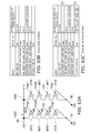
- FIG. 63A is a schematic circuit diagram showing the selection NAND string and the non-selection NAND string
- FIG. 63B shows a potential applied to the selection NAND string
- FIG. 63C shows a potential applied to the non-selection NAND string.
- FIG. 63A the case where data are read out from one memory cell transistor MT will be described.
- this memory cell transistor MT is described as “selection cell MT0", and the memory cell transistor MT other than that is described as “non-selection cell MT1".
- the NAND string NS including the selection cell MT0 is described as “selection string NS0”, and the NAND string NS other than that is described as “non-selection string NS1".
- FIG. 63B and FIG. 63C show potentials applied to the selection NAND string NS0 and the non-selection NAND string NS1 which is connected to the same bit line.
- V Volt
- Vbl bit line potential
- a relatively low source potential output from the low potential output circuit LVG for example, 0 V (zero volt) is applied to the source line SL connected to the selection string NS0 as the source line potential Vsl.
- a low potential difference of approximately 0.2 to 0.5 V is applied between the bit line 29 connected to the selection string NS0 and the source line SL.
- 2.5 to 4 V is applied to the selection gate lines SGD and SGS as selection gate potentials Vsgd and Vsgs.
- the upper selection transistor STD and the lower selection transistor STS of the selection string NS0 come into ON state, respectively.
- the read out potential Vread is a potential such that the memory cell transistor MT comes into ON state with no relation to a value held by the memory cell transistor MT.
- a potential lower than the read out potential Vread for example, 0 to 5 V is applied to the selection word line WL forming the selection cell MT0 as a word line potential Vwl.
- the word line potential Vwl is a potential such that a conduction state of the memory cell transistor MT is different depending on the value held by the memory cell transistor MT. In this state, a current passing through between the bit line 29 and the source line SL via the selection string NS0 is detected, and thereby a value programed into the selection cell MT0 can be read out.
- a voltage is caused to be applied to the non-selection string NS connected to the same bit line 29 as the selection string NS0 between the bit line 29 and the source line SL as well as the selection string NS0.
- 0 V is applied to the selection gate line SGD of the non-selection string NS1 as the selection gate potential Vsgd.
- the upper selection transistor STD comes into OFF state and a current can be suppressed from passing through the non-selection string NS1.
- the lower selection transistor STS of the non-selection string NS1 comes into OFF state. For this reason, the source potential Vsl is applied to the silicon pillar 20 of the non-selection string NS1. Because the same potential is applied to the word lines WL in the same level, the read out potential Vread or the word line potential Vwl is applied also to the word line WL of the non-selection string NS1.
- a voltage higher than the source line SL connected to the selection string NS0 (hereinafter referred to as “selection source line”) is applied to the source line SL connected to the non-selection string NS1 (hereinafter, referred to as “non-selection source line”) as the source line potential Vsl. More specifically, the relatively high source potential output from the high potential output circuit HVG is applied to the non-selection source line.
- the potential of the non-selection source line is set to be higher than the potential of the selection source line, it is possible that the voltage applied between the silicon pillar 20 and the word line WL is relaxed in the non-selection cell MT1, and the read disturb is suppressed.
- the ground potential (0 V) is applied to the selection source line, and 4.5 to 7 V is applied to the word line WL as the read out voltage Vread, a potential higher than 0 V, preferably, a potential of 1 V or higher is applied to the non-selection source line.
- the potential of the non-selection source line may be equal to the selection gate potential Vsgs.
- the lower selection transistor STS of the non-selection string NS1 comes into OFF state.
- the silicon pillar 20 is separated from the source line SL and the bit line 29 to come into a floating state.
- Coupling with the word line WL increases the potential of the silicon pillar 20 to near the read out potential Vread. This also reduces the voltage between the silicon pillar 20 and the word line WL.
- the same potential is applied to all source lines SL.
- the embodiment by dividing the cell source line 15 into multiple source lines SL, a potential higher than the selection source line connected to the selection string can be applied to the non-selection source line connected to the non-selection string. Thereby, it is possible that the voltage between the silicon pillar 20 and the word line WL is relaxed in the non-selection string and the read disturb is suppressed.
- FIG. 64 is a cross-sectional view showing a semiconductor memory device according to the embodiment.
- FIG. 65 shows the connection relationship of cell source lines in the semiconductor memory device according to the embodiment.
- one source line SL is provided every two rows NAND strings NS arranged along the Y-direction. That is, the multiple silicon pillars 20 arranged along the Y-direction are connected to the same source line SL, and the two adjacent silicon pillars 20 in the X-direction are connected to the same source line SL. For example, the two silicon pillars 20 sandwiching the interlayer insulating film 23 is connected to the same source line SL.
- each source line SL can be thick in comparison with the sixth embodiment described above, an interconnection resistance of the each source line SL can be reduced. This allows the semiconductor memory device 7 to operate with a high speed.
- FIG. 66 is a cross-sectional view showing a semiconductor memory device according to the embodiment.
- FIG. 67 shows the connection relationship of cell source lines in the semiconductor memory device according to the embodiment.
- the semiconductor memory device 8 there are two source lines SL belonging to each block Blk, and the source lines SL are shared in the adjacent blocks Blk. That is, the number of source lines SL is the same as the number of blocks Blk, and the source line and the block are arranged to be shifted by a half cycle.
- a conductive member 18 is provided in the trench 58 (see FIG. 11A) disposed between the blocks Blk.
- a group of the source lines SL which belong to the adjacent blocks Blk and are connected each other are disposed at a position sandwiching the conductive member 18.
- the conductive member 18 is plate-shaped and extends along the YZ plane, and its lower end is connected to the source line SL.
- An insulating film 19 is provided on both side surfaces of the conductive member 18, and isolates the conductive member 18 from the control gate electrode film 21.
- the source line SL connected to the conductive member 18 is connected to the silicon pillar 20 disposed on both sides in the X-direction viewed from the conductive member 18.
- An upper layer source line 30 extending in the Y-direction is provided on the conductive member 18 and connected to an upper end of the conductive member 18.
- the upper layer source line 30 is possible to be connected to the high potential output circuit HVG and the low potential output circuit LVG. Thereby, the source potential is supplied to the source line SL from the high potential output circuit HVG or the low potential output circuit LVG via the upper layer source line 30 and the conductive member 18.
- the resistance of the source line SL can be further reduced in comparison with the sixth and seventh embodiments.
- the sixth embodiment because a relatively high source potential can be applied to all source lines other than the source line SL connected to the selection string NS0 in each block Blk, the read disturb can be effectively suppressed.
- FIG. 68 is a perspective view showing a semiconductor memory device according to the embodiment.
- the cell source line 15 (see FIG. 1 and FIG. 2) is not provided, and the lower end of the silicon pillar 20 is connected to the silicon substrate 10.
- An impurity is introduced into an upper portion of the silicon substrate 10 and the upper portion is conductive.
- the upper portion of the silicon substrate 10 functions as the source line.
- the conductive member 18 (see FIG. 66) is provided in the trench 58 (see FIG. 11A) disposed between the blocks Blk, and the source potential can be applied to the silicon substrate 10.
- the cell source line can be omitted in comparison with the first embodiment described above.
- a contact layer having an impurity concentration higher than the periphery may be formed in a region directly below the trench 53 (see FIG. 9A) in the silicon substrate 10.
- FIG. 69 is a perspective view showing a semiconductor memory device according to the embodiment.
- the cell source line 15 (see FIG. 1 and FIG. 2) is not provided, and the lower ends of the two adjacent silicon pillars 20 in the X-direction are connected.
- a source line 49 extending in the Y-direction is provided between the interconnection 27 and the bit line 29.
- Out of two silicon pillars 20 having the lower ends connected one is connected to the bit line 29 via the via 28, and another one is connected to the source line 49.
- an U-shaped silicon member made of the two silicon pillars 20 is connected between the bit line 29 an d the source line 49.
- the source line 49 can be formed. For this reason, a material of the source line 49 is slightly restricted by the subsequent process, and a degree of freedom of material selection is high. Thereby, for example, the source line 49 can be formed of a metal material having a relatively low melting point. As a result, for example, the interconnection resistance of the source line 49 is easily reduced.
- a semiconductor memory device having good data retention characteristics and a method for manufacturing the semiconductor memory device can be realized.
Landscapes
- Engineering & Computer Science (AREA)
- Microelectronics & Electronic Packaging (AREA)
- Non-Volatile Memory (AREA)
- Semiconductor Memories (AREA)
- Physics & Mathematics (AREA)
- Geometry (AREA)
Abstract
L'invention concerne, selon un mode de réalisation, un dispositif de mémoire à semi-conducteur incluant un substrat, une colonne à semi-conducteur agencée sur le substrat destinée à s'étendre dans une direction verticale, une pluralité de premiers films d'électrode agencés latéralement par rapport à la colonne à semi-conducteur afin de s'étendre dans une première direction. La pluralité de premiers films d'électrode sont disposés afin d'être séparés les uns des autres le long de la direction verticale. La dispositif de mémoire à semi-conducteur comprend en outre une pluralité de seconds films d'électrode agencés entre la colonne à semi-conducteur et les premiers films d'électrode. La pluralité de seconds films d'électrode sont disposés afin d'être séparés les uns des autres le long de la direction verticale. Le dispositif de mémoire à semi-conducteur comprend en outre un premier film isolant agencé entre la colonne à semi-conducteur et les seconds films d'électrode, et un second film isolant agencé entre le second film d'électrode et le premier film d'électrode.
Priority Applications (9)
| Application Number | Priority Date | Filing Date | Title |
|---|---|---|---|
| CN201911282806.3A CN110943088B (zh) | 2014-01-10 | 2015-01-07 | 半导体存储装置及其制造方法 |
| CN201580004157.4A CN106165098A (zh) | 2014-01-10 | 2015-01-07 | 半导体存储装置及其制造方法 |
| TW108130020A TWI714228B (zh) | 2014-01-10 | 2015-01-09 | 半導體記憶體裝置 |
| TW106119372A TWI673830B (zh) | 2014-01-10 | 2015-01-09 | 半導體記憶體裝置 |
| TW104100803A TWI599022B (zh) | 2014-01-10 | 2015-01-09 | 半導體記憶體裝置及其製造方法 |
| US15/205,954 US10242992B2 (en) | 2014-01-10 | 2016-07-08 | Semiconductor memory device |
| US15/929,102 US10763272B2 (en) | 2014-01-10 | 2019-02-05 | Semiconductor memory device |
| US16/943,498 US11374015B2 (en) | 2014-01-10 | 2020-07-30 | Semiconductor memory device |
| US17/827,107 US20220285380A1 (en) | 2014-01-10 | 2022-05-27 | Semiconductor memory device |
Applications Claiming Priority (6)
| Application Number | Priority Date | Filing Date | Title |
|---|---|---|---|
| JP2014003793A JP2017010951A (ja) | 2014-01-10 | 2014-01-10 | 半導体記憶装置及びその製造方法 |
| JP2014-003793 | 2014-01-10 | ||
| US14/204,623 US20150200199A1 (en) | 2014-01-10 | 2014-03-11 | Semiconductor memory device and method for manufacturing same |
| US14/204,623 | 2014-03-11 | ||
| CN201410250359.4 | 2014-06-06 | ||
| CN201410250359.4A CN104779253B (zh) | 2014-01-10 | 2014-06-06 | 半导体存储装置及其制造方法 |
Related Parent Applications (1)
| Application Number | Title | Priority Date | Filing Date |
|---|---|---|---|
| US14/204,623 Continuation US20150200199A1 (en) | 2014-01-10 | 2014-03-11 | Semiconductor memory device and method for manufacturing same |
Related Child Applications (1)
| Application Number | Title | Priority Date | Filing Date |
|---|---|---|---|
| US15/205,954 Continuation US10242992B2 (en) | 2014-01-10 | 2016-07-08 | Semiconductor memory device |
Publications (2)
| Publication Number | Publication Date |
|---|---|
| WO2015105049A2 true WO2015105049A2 (fr) | 2015-07-16 |
| WO2015105049A3 WO2015105049A3 (fr) | 2015-10-22 |
Family
ID=53524450
Family Applications (1)
| Application Number | Title | Priority Date | Filing Date |
|---|---|---|---|
| PCT/JP2015/000044 Ceased WO2015105049A2 (fr) | 2014-01-10 | 2015-01-07 | Dispositif de mémoire à semi-conducteur et son procédé de fabrication |
Country Status (2)
| Country | Link |
|---|---|
| US (1) | US20220285380A1 (fr) |
| WO (1) | WO2015105049A2 (fr) |
Cited By (5)
| Publication number | Priority date | Publication date | Assignee | Title |
|---|---|---|---|---|
| US9984754B2 (en) | 2014-09-29 | 2018-05-29 | Toshiba Memory Corporation | Memory device and method for operating the same |
| US10002880B1 (en) | 2017-03-30 | 2018-06-19 | Toshiba Memory Corporation | Semiconductor device and method for manufacturing same |
| JP2020518135A (ja) * | 2017-04-28 | 2020-06-18 | マイクロン テクノロジー,インク. | メモリ・セルの高さ方向に延びるストリングのアレイ、およびメモリ・アレイを形成する方法 |
| US11682667B2 (en) | 2017-06-27 | 2023-06-20 | Semiconductor Energy Laboratory Co., Ltd. | Memory cell including cell transistor including control gate and charge accumulation layer |
| US12219771B2 (en) | 2019-07-05 | 2025-02-04 | Semiconductor Energy Laboratory Co., Ltd. | Semiconductor device using oxide and method for manufacturing semiconductor device using oxide |
Families Citing this family (3)
| Publication number | Priority date | Publication date | Assignee | Title |
|---|---|---|---|---|
| US10680006B2 (en) | 2017-08-11 | 2020-06-09 | Micron Technology, Inc. | Charge trap structure with barrier to blocking region |
| US10446572B2 (en) | 2017-08-11 | 2019-10-15 | Micron Technology, Inc. | Void formation for charge trap structures |
| US10164009B1 (en) * | 2017-08-11 | 2018-12-25 | Micron Technology, Inc. | Memory device including voids between control gates |
Family Cites Families (6)
| Publication number | Priority date | Publication date | Assignee | Title |
|---|---|---|---|---|
| KR101495806B1 (ko) * | 2008-12-24 | 2015-02-26 | 삼성전자주식회사 | 비휘발성 기억 소자 |
| KR101652873B1 (ko) * | 2010-02-18 | 2016-08-31 | 삼성전자주식회사 | 3차원 반도체 장치 및 그 동작 방법 |
| US8198672B2 (en) * | 2010-06-30 | 2012-06-12 | SanDisk Technologies, Inc. | Ultrahigh density vertical NAND memory device |
| US8722525B2 (en) * | 2011-06-21 | 2014-05-13 | Micron Technology, Inc. | Multi-tiered semiconductor devices and associated methods |
| US8946023B2 (en) * | 2013-03-12 | 2015-02-03 | Sandisk Technologies Inc. | Method of making a vertical NAND device using sequential etching of multilayer stacks |
| JP2017010951A (ja) * | 2014-01-10 | 2017-01-12 | 株式会社東芝 | 半導体記憶装置及びその製造方法 |
-
2015
- 2015-01-07 WO PCT/JP2015/000044 patent/WO2015105049A2/fr not_active Ceased
-
2022
- 2022-05-27 US US17/827,107 patent/US20220285380A1/en not_active Abandoned
Non-Patent Citations (1)
| Title |
|---|
| None |
Cited By (6)
| Publication number | Priority date | Publication date | Assignee | Title |
|---|---|---|---|---|
| US9984754B2 (en) | 2014-09-29 | 2018-05-29 | Toshiba Memory Corporation | Memory device and method for operating the same |
| US10002880B1 (en) | 2017-03-30 | 2018-06-19 | Toshiba Memory Corporation | Semiconductor device and method for manufacturing same |
| JP2020518135A (ja) * | 2017-04-28 | 2020-06-18 | マイクロン テクノロジー,インク. | メモリ・セルの高さ方向に延びるストリングのアレイ、およびメモリ・アレイを形成する方法 |
| US11682667B2 (en) | 2017-06-27 | 2023-06-20 | Semiconductor Energy Laboratory Co., Ltd. | Memory cell including cell transistor including control gate and charge accumulation layer |
| US12125849B2 (en) | 2017-06-27 | 2024-10-22 | Semiconductor Energy Laboratory Co., Ltd. | Semiconductor device, semiconductor wafer, memory device, and electronic device |
| US12219771B2 (en) | 2019-07-05 | 2025-02-04 | Semiconductor Energy Laboratory Co., Ltd. | Semiconductor device using oxide and method for manufacturing semiconductor device using oxide |
Also Published As
| Publication number | Publication date |
|---|---|
| US20220285380A1 (en) | 2022-09-08 |
| WO2015105049A3 (fr) | 2015-10-22 |
Similar Documents
| Publication | Publication Date | Title |
|---|---|---|
| US11374015B2 (en) | Semiconductor memory device | |
| US20220285380A1 (en) | Semiconductor memory device | |
| US11849586B2 (en) | Semiconductor device and method of manufacturing the same | |
| US11888041B2 (en) | Nonvolatile semiconductor memory device including a memory cell | |
| US10249635B2 (en) | Three-dimensional semiconductor memory device and method for manufacturing the same | |
| CN102769018B (zh) | 非易失性存储器件 | |
| US9865616B2 (en) | Semiconductor memory device and method for manufacturing same | |
| US11985822B2 (en) | Memory device | |
| US10249641B2 (en) | Semiconductor memory device and method for manufacturing same | |
| US10043815B2 (en) | Semiconductor memory device | |
| JP2015060874A (ja) | 不揮発性半導体記憶装置 | |
| US9806092B1 (en) | Semiconductor memory device and methods for manufacturing the same | |
| US20170263629A1 (en) | Semiconductor memory device | |
| US20160268296A1 (en) | Semiconductor memory device and method for manufacturing same | |
| US11018150B2 (en) | Semiconductor memory device including artificial drain select gate and method for driving same | |
| TWI865887B (zh) | 半導體裝置及其製造方法 | |
| US12302566B2 (en) | Semiconductor memory device and method for manufacturing the same | |
| JP2011171755A (ja) | 半導体装置 |
Legal Events
| Date | Code | Title | Description |
|---|---|---|---|
| 121 | Ep: the epo has been informed by wipo that ep was designated in this application |
Ref document number: 15713240 Country of ref document: EP Kind code of ref document: A2 |
|
| NENP | Non-entry into the national phase |
Ref country code: DE |
|
| NENP | Non-entry into the national phase |
Ref country code: JP |
|
| 122 | Ep: pct application non-entry in european phase |
Ref document number: 15713240 Country of ref document: EP Kind code of ref document: A2 |