WO2015105171A1 - Dispositif d'alimentation électrique haute tension - Google Patents
Dispositif d'alimentation électrique haute tension Download PDFInfo
- Publication number
- WO2015105171A1 WO2015105171A1 PCT/JP2015/050466 JP2015050466W WO2015105171A1 WO 2015105171 A1 WO2015105171 A1 WO 2015105171A1 JP 2015050466 W JP2015050466 W JP 2015050466W WO 2015105171 A1 WO2015105171 A1 WO 2015105171A1
- Authority
- WO
- WIPO (PCT)
- Prior art keywords
- voltage
- switching element
- transformer
- circuit
- output voltage
- Prior art date
- Legal status (The legal status is an assumption and is not a legal conclusion. Google has not performed a legal analysis and makes no representation as to the accuracy of the status listed.)
- Ceased
Links
Images

Classifications
-
- H—ELECTRICITY
- H02—GENERATION; CONVERSION OR DISTRIBUTION OF ELECTRIC POWER
- H02M—APPARATUS FOR CONVERSION BETWEEN AC AND AC, BETWEEN AC AND DC, OR BETWEEN DC AND DC, AND FOR USE WITH MAINS OR SIMILAR POWER SUPPLY SYSTEMS; CONVERSION OF DC OR AC INPUT POWER INTO SURGE OUTPUT POWER; CONTROL OR REGULATION THEREOF
- H02M3/00—Conversion of DC power input into DC power output
- H02M3/22—Conversion of DC power input into DC power output with intermediate conversion into AC
- H02M3/24—Conversion of DC power input into DC power output with intermediate conversion into AC by static converters
- H02M3/28—Conversion of DC power input into DC power output with intermediate conversion into AC by static converters using discharge tubes with control electrode or semiconductor devices with control electrode to produce the intermediate AC
- H02M3/325—Conversion of DC power input into DC power output with intermediate conversion into AC by static converters using discharge tubes with control electrode or semiconductor devices with control electrode to produce the intermediate AC using devices of a triode or a transistor type requiring continuous application of a control signal
- H02M3/335—Conversion of DC power input into DC power output with intermediate conversion into AC by static converters using discharge tubes with control electrode or semiconductor devices with control electrode to produce the intermediate AC using devices of a triode or a transistor type requiring continuous application of a control signal using semiconductor devices only
-
- H—ELECTRICITY
- H02—GENERATION; CONVERSION OR DISTRIBUTION OF ELECTRIC POWER
- H02M—APPARATUS FOR CONVERSION BETWEEN AC AND AC, BETWEEN AC AND DC, OR BETWEEN DC AND DC, AND FOR USE WITH MAINS OR SIMILAR POWER SUPPLY SYSTEMS; CONVERSION OF DC OR AC INPUT POWER INTO SURGE OUTPUT POWER; CONTROL OR REGULATION THEREOF
- H02M1/00—Details of apparatus for conversion
- H02M1/44—Circuits or arrangements for compensating for electromagnetic interference in converters or inverters
-
- H—ELECTRICITY
- H02—GENERATION; CONVERSION OR DISTRIBUTION OF ELECTRIC POWER
- H02M—APPARATUS FOR CONVERSION BETWEEN AC AND AC, BETWEEN AC AND DC, OR BETWEEN DC AND DC, AND FOR USE WITH MAINS OR SIMILAR POWER SUPPLY SYSTEMS; CONVERSION OF DC OR AC INPUT POWER INTO SURGE OUTPUT POWER; CONTROL OR REGULATION THEREOF
- H02M3/00—Conversion of DC power input into DC power output
- H02M3/02—Conversion of DC power input into DC power output without intermediate conversion into AC
- H02M3/04—Conversion of DC power input into DC power output without intermediate conversion into AC by static converters
- H02M3/10—Conversion of DC power input into DC power output without intermediate conversion into AC by static converters using discharge tubes with control electrode or semiconductor devices with control electrode
- H02M3/145—Conversion of DC power input into DC power output without intermediate conversion into AC by static converters using discharge tubes with control electrode or semiconductor devices with control electrode using devices of a triode or transistor type requiring continuous application of a control signal
- H02M3/155—Conversion of DC power input into DC power output without intermediate conversion into AC by static converters using discharge tubes with control electrode or semiconductor devices with control electrode using devices of a triode or transistor type requiring continuous application of a control signal using semiconductor devices only
- H02M3/156—Conversion of DC power input into DC power output without intermediate conversion into AC by static converters using discharge tubes with control electrode or semiconductor devices with control electrode using devices of a triode or transistor type requiring continuous application of a control signal using semiconductor devices only with automatic control of output voltage or current, e.g. switching regulators
- H02M3/158—Conversion of DC power input into DC power output without intermediate conversion into AC by static converters using discharge tubes with control electrode or semiconductor devices with control electrode using devices of a triode or transistor type requiring continuous application of a control signal using semiconductor devices only with automatic control of output voltage or current, e.g. switching regulators including plural semiconductor devices as final control devices for a single load
-
- H—ELECTRICITY
- H02—GENERATION; CONVERSION OR DISTRIBUTION OF ELECTRIC POWER
- H02M—APPARATUS FOR CONVERSION BETWEEN AC AND AC, BETWEEN AC AND DC, OR BETWEEN DC AND DC, AND FOR USE WITH MAINS OR SIMILAR POWER SUPPLY SYSTEMS; CONVERSION OF DC OR AC INPUT POWER INTO SURGE OUTPUT POWER; CONTROL OR REGULATION THEREOF
- H02M3/00—Conversion of DC power input into DC power output
- H02M3/22—Conversion of DC power input into DC power output with intermediate conversion into AC
- H02M3/24—Conversion of DC power input into DC power output with intermediate conversion into AC by static converters
- H02M3/28—Conversion of DC power input into DC power output with intermediate conversion into AC by static converters using discharge tubes with control electrode or semiconductor devices with control electrode to produce the intermediate AC
- H02M3/325—Conversion of DC power input into DC power output with intermediate conversion into AC by static converters using discharge tubes with control electrode or semiconductor devices with control electrode to produce the intermediate AC using devices of a triode or a transistor type requiring continuous application of a control signal
- H02M3/335—Conversion of DC power input into DC power output with intermediate conversion into AC by static converters using discharge tubes with control electrode or semiconductor devices with control electrode to produce the intermediate AC using devices of a triode or a transistor type requiring continuous application of a control signal using semiconductor devices only
- H02M3/33507—Conversion of DC power input into DC power output with intermediate conversion into AC by static converters using discharge tubes with control electrode or semiconductor devices with control electrode to produce the intermediate AC using devices of a triode or a transistor type requiring continuous application of a control signal using semiconductor devices only with automatic control of the output voltage or current, e.g. flyback converters
-
- H—ELECTRICITY
- H02—GENERATION; CONVERSION OR DISTRIBUTION OF ELECTRIC POWER
- H02M—APPARATUS FOR CONVERSION BETWEEN AC AND AC, BETWEEN AC AND DC, OR BETWEEN DC AND DC, AND FOR USE WITH MAINS OR SIMILAR POWER SUPPLY SYSTEMS; CONVERSION OF DC OR AC INPUT POWER INTO SURGE OUTPUT POWER; CONTROL OR REGULATION THEREOF
- H02M7/00—Conversion of AC power input into DC power output; Conversion of DC power input into AC power output
- H02M7/42—Conversion of DC power input into AC power output without possibility of reversal
- H02M7/44—Conversion of DC power input into AC power output without possibility of reversal by static converters
- H02M7/48—Conversion of DC power input into AC power output without possibility of reversal by static converters using discharge tubes with control electrode or semiconductor devices with control electrode
- H02M7/53—Conversion of DC power input into AC power output without possibility of reversal by static converters using discharge tubes with control electrode or semiconductor devices with control electrode using devices of a triode or transistor type requiring continuous application of a control signal
- H02M7/537—Conversion of DC power input into AC power output without possibility of reversal by static converters using discharge tubes with control electrode or semiconductor devices with control electrode using devices of a triode or transistor type requiring continuous application of a control signal using semiconductor devices only, e.g. single switched pulse inverters
-
- H—ELECTRICITY
- H02—GENERATION; CONVERSION OR DISTRIBUTION OF ELECTRIC POWER
- H02M—APPARATUS FOR CONVERSION BETWEEN AC AND AC, BETWEEN AC AND DC, OR BETWEEN DC AND DC, AND FOR USE WITH MAINS OR SIMILAR POWER SUPPLY SYSTEMS; CONVERSION OF DC OR AC INPUT POWER INTO SURGE OUTPUT POWER; CONTROL OR REGULATION THEREOF
- H02M1/00—Details of apparatus for conversion
- H02M1/0048—Circuits or arrangements for reducing losses
- H02M1/0054—Transistor switching losses
- H02M1/0058—Transistor switching losses by employing soft switching techniques, i.e. commutation of transistors when applied voltage is zero or when current flow is zero
-
- H—ELECTRICITY
- H02—GENERATION; CONVERSION OR DISTRIBUTION OF ELECTRIC POWER
- H02M—APPARATUS FOR CONVERSION BETWEEN AC AND AC, BETWEEN AC AND DC, OR BETWEEN DC AND DC, AND FOR USE WITH MAINS OR SIMILAR POWER SUPPLY SYSTEMS; CONVERSION OF DC OR AC INPUT POWER INTO SURGE OUTPUT POWER; CONTROL OR REGULATION THEREOF
- H02M7/00—Conversion of AC power input into DC power output; Conversion of DC power input into AC power output
- H02M7/42—Conversion of DC power input into AC power output without possibility of reversal
- H02M7/44—Conversion of DC power input into AC power output without possibility of reversal by static converters
- H02M7/48—Conversion of DC power input into AC power output without possibility of reversal by static converters using discharge tubes with control electrode or semiconductor devices with control electrode
- H02M7/4815—Resonant converters
-
- Y—GENERAL TAGGING OF NEW TECHNOLOGICAL DEVELOPMENTS; GENERAL TAGGING OF CROSS-SECTIONAL TECHNOLOGIES SPANNING OVER SEVERAL SECTIONS OF THE IPC; TECHNICAL SUBJECTS COVERED BY FORMER USPC CROSS-REFERENCE ART COLLECTIONS [XRACs] AND DIGESTS
- Y02—TECHNOLOGIES OR APPLICATIONS FOR MITIGATION OR ADAPTATION AGAINST CLIMATE CHANGE
- Y02B—CLIMATE CHANGE MITIGATION TECHNOLOGIES RELATED TO BUILDINGS, e.g. HOUSING, HOUSE APPLIANCES OR RELATED END-USER APPLICATIONS
- Y02B70/00—Technologies for an efficient end-user side electric power management and consumption
- Y02B70/10—Technologies improving the efficiency by using switched-mode power supplies [SMPS], i.e. efficient power electronics conversion e.g. power factor correction or reduction of losses in power supplies or efficient standby modes
Definitions
- the present invention relates to a high-voltage power supply device used in, for example, an ion generator, an ozone generator, an electronic device using a high voltage, and the like.
- Patent Document 1 includes a high-voltage transformer, a transistor connected to the primary coil of the high-voltage transformer, and a feedback control circuit connected to the secondary coil of the high-voltage transformer.
- a circuit is shown in which a sine wave voltage is generated in the secondary coil of the high-voltage transformer by performing ON / OFF control of the transistor based on the induced voltage of the secondary coil.
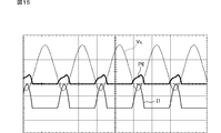
- FIG. 15 shows typical current / voltage waveforms for transistor loss.
- the product of the collector voltage Vc and the primary coil current I1 of the high-voltage transformer is the loss Pl generated in the transistor.
- the base current is feedback-controlled so that the output voltage becomes constant. Therefore, when the input voltage increases, the increase increases as a loss as it is. Further, the transistor can be completely turned on / off, but in that case, switching noise occurs.
- An object of the present invention is to provide a high-voltage power supply device in which a loss and switching noise in a switching element that switches a current of a primary coil of a high-voltage transformer are reduced, and to easily control an output voltage without increasing the loss.
- An object of the present invention is to provide a high-voltage power supply device that can be used.
- a high-voltage power supply device includes a high-voltage transformer having a primary coil and a secondary coil, a switching element that switches and drives the primary coil of the high-voltage transformer, and pulse-drives the switching element.
- a switching control circuit for continuously energizing the transformer by turning on and replenishing energy by the amount of excitation until turning off, and continuously performing the resonance operation by the secondary coil and distributed capacity;
- the switching control circuit turns on the switching element during a period in which the phase of the resonance voltage pulse applied to the switching element is 90 ° to 270 ° when the switching element is turned off, and then determines the leakage inductance and distributed capacitance of the high-voltage transformer.
- the switching element is turned off in the vicinity where the polarity of the current of the generated harmonic vibration becomes zero.
- the switching control circuit controls the output voltage of the high voltage transformer by controlling the on-timing of the switching element (the output voltage is increased by advancing the on-timing and the output voltage is decreased by delaying the on-timing).
- an output voltage control circuit Preferably, an output voltage control circuit.
- the output voltage control circuit includes an offset circuit that superimposes an offset voltage that increases as the output voltage rises on the output voltage of the high-voltage transformer, and the offset voltage is superimposed. It is preferable to include a zero-cross detection circuit that detects a zero-cross timing of the voltage as an on-timing of the switching element. As a result, the output voltage can be kept constant, and a stable high voltage can be supplied to the load.
- the switching control circuit adjusts the output voltage by PWM control of the switching element according to the current flowing in the primary coil or the secondary coil of the transformer. It is preferable to provide a PWM control circuit that stabilizes. Thereby, for example, a phenomenon in which the output voltage rises abnormally at light load can be prevented, or the output voltage can be lowered at heavy load, and the like, so that a more stable operation can be achieved.
- the loss in the switching element that switches the current of the primary coil of the high-voltage transformer is reduced, and the switching noise is reduced.
- a high-efficiency and low-noise high-voltage power supply device can be obtained.
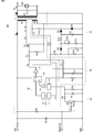
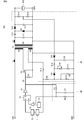
- FIG. 1 is a circuit diagram of a high-voltage power supply device 101 according to the first embodiment.
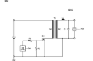
- FIG. 2 is a simplified circuit diagram of the high-voltage power supply device according to the first embodiment.
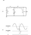
- 3A is an equivalent circuit diagram of the high-voltage power supply device 101
- FIG. 3B is a waveform diagram of each part of FIG. 3A.
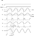
- FIG. 4 is a waveform diagram of each part of FIG.
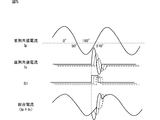
- FIG. 5 is a diagram showing a change in the resonance current waveform when the turn-on / off timing of the switch S1 in the equivalent circuit shown in FIG.
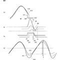
- FIG. 6 is a waveform diagram showing voltage control.
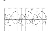
- FIG. 7 is a waveform diagram of each part of the high-voltage power supply device 101.
- FIG. 1 is a circuit diagram of a high-voltage power supply device 101 according to the first embodiment.
- FIG. 2 is a simplified circuit diagram of the high-voltage power supply device according to the first embodiment.
- 3A is an equivalent circuit diagram of the high
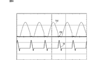
- FIG. 8 is a waveform diagram showing the loss in the switching element Q1.
- FIG. 9 is a circuit diagram of the high-voltage power supply apparatus 102 according to the second embodiment.
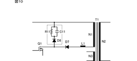
- FIG. 10 is a diagram illustrating a part of a circuit of a high-voltage power supply device according to the third embodiment.
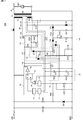
- FIG. 11 is a circuit diagram of the high-voltage power supply device 104 according to the fourth embodiment.
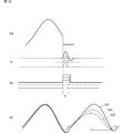
- FIG. 12 is a waveform diagram of each part of the high-voltage power supply device 104.
- FIG. 13 is a waveform diagram of each part of the high-voltage power supply device 104.
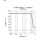
- FIG. 14 is a diagram illustrating an example of a change in the output voltage V2 due to the load weight of the high-voltage power supply device 104.
- FIG. 15 is a typical current / voltage waveform diagram of transistor loss in a conventional high-voltage power supply device.
- FIG. 1 is a circuit diagram of a high-voltage power supply device 101 according to the first embodiment
- FIG. 2 is a simplified circuit diagram of the high-voltage power supply device according to the first embodiment.
- a switching element Q1 is connected to a primary coil N1 of a high-voltage transformer (hereinafter simply referred to as “transformer”) T1.
- a switching control circuit 90 is connected to the gate of the switching element Q1.
- An ozone generating element 201 as an AC high voltage load is connected to the secondary coil N2 of the transformer T1.
- Le shows the leakage inductance of the transformer T1 as a circuit element
- the capacitor C1 shows the distributed capacitance of the high-voltage transformer T1 and the ozone generating element 201 as a circuit element.
- the capacitor C1 may be externally attached.
- the switching control circuit 90 turns on the switching element Q1
- a current drain current
- the transformer T1 is excited.
- a resonance current flows through a resonance circuit including the distributed capacitor C1 and the secondary coil N2 due to the excitation energy of the transformer T1, and a resonance voltage is generated at both ends of the distributed capacitor C1.
- the range of 0 ° to 90 ° and 270 ° to 360 ° corresponds to the charging period to the distributed capacitor C1
- the range of 90 ° to 270 ° corresponds to the discharging period.
- the switching frequency of the switching element Q1 is higher than the resonance frequency of the resonance circuit. Therefore, the switching element Q1 is turned on before the resonance voltage pulse (one peak) is finished.
- the switching element Q1 is turned on at a timing within the range of 90 ° to 270 ° in the phase of the resonance voltage pulse, that is, the discharge period of the distributed capacitor C1, thereby forcibly from the distributed capacitor C1 via the leakage inductance Le. By extracting the current, it is possible to supply the energy for the resonance operation and to continue the resonance operation.
- FIG. 3A is an equivalent circuit diagram of the high-voltage power supply device 101, and FIG. 3B is a waveform diagram of each part of FIG. 3A.
- the transformer T1 and the leakage inductance Le in FIG. 2 are represented by a T-type circuit including an excitation inductance Lp and leakage inductances La and Lb shown in FIG. Further, the switching element Q1 in FIG. 2 is represented by a switch S1 shown in FIG. 3A, and the ozone generating element 201 in FIG. 2 is represented by a load resistor R4 shown in FIG.
- the switch S1 is turned on while the switch S1 is off and the parallel resonance current (harmonic vibration) Ip due to the inductances Lp and Lb and the distributed capacitance C1 is flowing, the series resonant current due to the inductances La and Lb and the distributed capacitance C1. Is flows.
- the switch S1 is turned on, so that series resonance occurs. Current Is is flowing.
- the above harmonic vibration is determined by the distributed capacitance C1 and the leakage inductances La and Lb. Since the energy is proportional to the electric charge accumulated in the distributed capacitor C1, until the lowest point of the sinusoidal oscillation seen by the drain voltage of the switching element Q1 shown in FIG. By turning on switching element Q1 (within a range of ⁇ 270 °), harmonic vibrations can be generated.
- the energy of harmonic vibration is determined by the potential remaining in the distributed capacity as a sinusoidal voltage.
- the output voltage can be controlled by superimposing the harmonic vibration on the main vibration (voltage due to parallel resonance) generated in the secondary coil N2 and the distributed capacitance C1 of the original transformer T1.
- the above sine wave voltage is stable, and as a result, harmonic vibration is also generated as a stable output, so that stable control is possible. Further, during the period in which the harmonic vibration is generated, the energy of the main vibration, that is, the energy extracted to the load is replenished at the same time. Therefore, the output voltage can be lowered by shortening the period.
- the switching control circuit includes a gate signal generation circuit 10, a remote switch circuit 20, a pulse width setting circuit 30, and an offset circuit 40.
- the transformer T1 of the high-voltage power supply device 101 shown in FIG. 1 includes a tertiary coil N3 for output voltage detection.
- the zero-cross detection circuit 11 detects the zero-cross of the output voltage of the tertiary coil N3, and the one-shot pulse generation circuit 12 uses the output signal of the zero-cross detection circuit 11 as a trigger to send the one-shot pulse to the flip-flop 15 To the set terminal.
- the reference voltage shift circuit 13 determines a reference voltage to be applied to the comparator 14 according to the output voltage of the remote switch circuit 20.
- the comparator 14 compares the output voltage of the pulse width setting circuit 30 with the output voltage (reference voltage) of the reference voltage shift circuit 13 and gives the result to the reset terminal of the flip-flop 15.
- the driver circuit 16 receives the output voltage of the flip-flop 15 and generates a gate signal Vg for the switching element Q1.
- the remote switch circuit 20 determines the input voltage of the reference voltage shift circuit 13 according to the potential of the remote terminal REMOTE.
- the remote switch circuit 20 includes resistors R3, R4, R5, a capacitor C6, and a transistor Q2.
- the reference voltage shift circuit 13 determines the reference voltage according to the level of the remote terminal REMOTE.
- the pulse width setting circuit 30 is a charge / discharge circuit based on the output voltage of the driver circuit 16.
- the pulse width setting circuit 30 includes resistors R6 and R7 and a capacitor C7.
- the output voltage of the driver circuit 16 becomes high level, the charging voltage of the capacitor C7 increases, and the + terminal input voltage of the comparator 14 increases.
- this voltage exceeds the output voltage of the reference voltage shift circuit 13, the flip-flop 15 is reset, and the output voltage of the driver circuit 16 returns to the low level. That is, the ON period of the switching element Q1 is determined by this operation.
- the offset circuit 40 is a circuit that shifts the level of the voltage signal applied to the zero-cross detection circuit 11. As will be shown later, the output voltage is controlled by the offset voltage, which stabilizes the output voltage.
- the offset circuit 40 includes capacitors C8, C9, C10, diodes D4, D5, D6, resistors R9, R10, R12, R13, R14, and a variable resistor VR1.
- the output voltage of the tertiary coil N3 of the transformer T1 is double-voltage rectified by capacitors C9 and C10 and diodes D5 and D6. As a result, a DC conversion voltage having a peak-to-peak value of the output voltage of the tertiary coil N3 is generated.
- This voltage is divided by resistors R12 and R14 and variable resistor VR1, and is smoothed by resistors R9 and R10 and capacitor C8. This smoothed voltage is superimposed on the output voltage of the tertiary coil N3 and applied to the zero-cross detection circuit 11.
- FIG. 4 is a waveform diagram of each part of FIG. The operation of the high-voltage power supply device 101 shown in FIG. 1 will be described with reference to FIG.
- the output voltage of the secondary coil N2, the output voltage of the tertiary coil N3, and the drain voltage Vd are each reverse in a sine wave form due to the discharge from the distributed capacitor C1.
- sinusoidal voltage vibration main vibration
- the frequency of the main vibration is, for example, 30 to 50 kHz.
- the flip-flop 15 When the output voltage V3 'of the offset circuit 40 reaches the timing t2 when it falls below the zero cross, the flip-flop 15 is set and the switching element Q1 is turned on. As a result, the charge of the distributed capacitor C1 is forcibly extracted during the return of the current from the distributed capacitor C1 to the secondary coil N2 (exciting the transformer T1 in the reverse direction) (the distributed capacitor C1 is forcibly discharged). ) As a result, the vibration mode changes transiently, and harmonic vibration occurs in the resonance circuit including the leakage inductance Le and the distributed capacitance C1. This vibration appears in the waveform of the drain current Id.
- the frequency of the harmonic vibration is, for example, 80 to 200 kHz.
- the reverse pulse voltage generated by the harmonic vibration is superimposed on the negative pulse of the main vibration, and the peak-peak value of the voltage vibration increases.
- the voltage level to be superimposed is determined by the voltage level of the distributed capacitor C1 at the time when the switching element Q1 is turned on. The higher the voltage timing, the larger the voltage to be superimposed. On the contrary, if the timing is low, the superimposed voltage becomes small.
- the output voltage can be controlled using this characteristic.
- the switching element Q1 is turned on at a timing within the phase range of 90 ° to 270 ° of the resonance voltage pulse (main vibration).
- the main vibration starts when the switching element Q1 is turned on. At the same time, the excitation of the primary coil N1 also starts, so that the energy of the harmonic vibration is continuously supplied and stable operation is possible.
- the switching element Q1 When the switching element Q1 is turned off at a timing t3 after a predetermined time has elapsed from t2, a reverse current starts to flow through the body diode of the switching element Q1, as shown in the waveform of the drain current Id. Thereafter, the current of the body diode is cut off at timing t4. Therefore, it is preferable to set the OFF timing of the switching element Q1 at around 180 ° in the phase of the harmonic oscillation period determined by the leakage inductance Le and the distributed capacitance C1. Between 180 ° and 360 ° (period in which the polarity of the harmonic vibration current is reversed), the turn-off is a soft switch (zero current switch) and a zero voltage switch. Is also small.
- the timing at which the switching element Q1 is turned off at such a phase that the effects of zero current switching and zero voltage switching occur is the meaning of “around 180 ° in the phase of the harmonic oscillation period”.
- FIG. 5 and 6 are waveform diagrams showing the voltage control.
- FIG. 5 shows changes in the resonance current waveform when the turn-on / off timing of the switch S1 is changed in the equivalent circuit shown in FIG.
- FIG. 6 shows an example in which the turn-on timing of the switching element Q1 is changed as t21, t22, and t23 as shown by three waveforms of the gate signal Vg.
- the series resonance current Is is superimposed on the main resonance current (parallel resonance current Ip). Therefore, as shown in FIG. 6, by changing the ON timing to t21, t22, and t23, as shown in the waveforms Id1, Id2, and Id3 of the drain current Id, between the leakage inductance Le and the distributed capacitance C1.
- the amplitude of the harmonic vibration that occurs in is changed. Accordingly, the output voltage V2 changes as indicated by V21, V22, and V23.
- the superimposed voltage can be controlled by controlling the turn-on timing within the range of 90 ° to 270 ° with the phase of the resonance voltage pulse (main vibration). As a result, the peak-peak value of the output voltage V2 is set to a predetermined value. Can be controlled.
- the offset circuit 40 shown in FIG. 1 superimposes an offset voltage that increases as the output voltage V3 increases on the output voltage V3 of the tertiary coil N3 that is a proportional value of the output voltage V2 to the load. Therefore, when the output voltage V3 decreases, the turn-on timing of the switching element Q1 is advanced, and as a result, the output voltage increases. When the output voltage V3 rises, the reverse operation causes the turn-on timing of the switching element Q1 to be delayed. By this action, the output voltage V2 to the load is stabilized.
- the ON period of the switching element Q1 is determined by the pulse width setting circuit 30.
- the ON period of the switching element Q1 is determined so as to be a soft switch (zero current switch) at the turn-off timings t31, t32, and t33.
- the on period of the switching element Q1 is determined so that when the turn-on is performed at the timing t21, the harmonic oscillation phase is turned off within a range of 180 ° to 360 °. Since the frequency of the harmonic vibration generated by the leakage inductance Le and the distributed capacitance C1 of the transformer T1 is constant, the ON period of the switching element Q1 can be fixed. It is also possible to detect and turn off the harmonic current pulse when it crosses zero, and a circuit capable of controlling in a wider range can be created.
- FIG. 7 is a waveform diagram of each part of the high-voltage power supply device 101.
- the load current I2 is also shown.
- a sinusoidal AC high voltage is applied to the load, and a sinusoidal AC current flows.
- the load of the high voltage power supply device is the ozone generating element 201, it is a capacitive load. Therefore, the phase of the current I2 is advanced by 90 ° from the voltage V2.
- FIG. 8 is a waveform diagram showing the loss in the switching element Q1.
- the product of the drain voltage Vd and the drain current Id becomes a loss in the switching element Q1, but since the switching element Q1 performs a soft switch and a zero voltage switch, a loss due to switching hardly occurs.
- the inductor L1 is connected in series to the primary coil N1 of the transformer T1, but the inductor L1 is not necessary if the leakage inductance of the transformer T1 is a predetermined value.
- the distributed capacitor C1 is illustrated as a circuit element in the secondary coil N2 of the transformer T1, but a capacitor as an actual component may be connected in parallel to the secondary coil N2 of the transformer T1.
- FIG. 9 is a circuit diagram of the high-voltage power supply apparatus 102 according to the second embodiment. Unlike the first embodiment, the high-voltage power supply apparatus 102 of this embodiment supplies a DC high voltage to the ion generating element 202 that is a DC load.
- the secondary coil N2 of the transformer T1 constitutes a resonance circuit with a leakage inductance Le and a capacitor C1, and a voltage doubler rectifier circuit with diodes D9 and D10 and capacitors C12 and C13. .
- a DC high voltage is supplied to the ion generating element 202.
- the offset circuit 40 includes resistors R12 and R13 that divide the load voltage.
- the other configuration of the offset circuit 40 is the same as that shown in FIG. Further, the configuration of the other circuit portions is the same as that shown in FIG.
- the output voltage of the secondary coil N2 of the transformer T1 is sinusoidal, it is asymmetrical between positive and negative. Therefore, the output voltage is stabilized by feedback control with high accuracy by performing double voltage rectification in this way to obtain a DC voltage. Can be done.
- FIG. 10 is a diagram illustrating a part of a circuit of a high-voltage power supply device according to the third embodiment.
- a switching element Q1 is connected in series to the primary coil N1 of the transformer T1, and a diode D7 and an inductor L1 are connected between the switching element Q1 and the first end of the primary coil N1.
- a snubber circuit including a capacitor C11, a resistor R11, and a diode D8 is connected between the drain of the switching element Q1 and the second end of the primary coil N1.
- the diode D7 prevents a resonance operation on the primary side of the transformer T1.
- the diode D7 may be connected to the second end side of the primary coil N1.
- the snubber circuit absorbs the back electromotive force even if a back electromotive force is generated in the primary coil of the transformer T1 when the switching element Q1 is turned off (a slight deviation from the timing of the zero current switch).
- the inductor L1 connected to the primary coil N1 may be connected to the switching element Q1 side.
- the zero cross of the electromotive voltage of the tertiary coil is detected and used as a trigger.
- the zero cross of the drain voltage of the switching element Q1 may be detected and used as a trigger. Good.
- FIG. 11 is a circuit diagram of the high-voltage power supply device 104 according to the fourth embodiment.
- the high-voltage power supply device 104 includes an AC pulse generation circuit 50.
- the AC pulse generation circuit 50 is a circuit for detecting the timing at which the output voltage (AC pulse) of the tertiary coil N3 of the transformer T1 crosses zero.
- the switching element Q1 is turned on at the timing when the AC pulse zero-crosses. This is the same as the high-voltage power supply devices 101 and 102 shown in the first and second embodiments.
- the high voltage power supply device 104 includes an offset circuit 40.
- the offset circuit 40 is a circuit for biasing the AC pulse with the rectified voltage of the AC pulse by utilizing the fact that the AC pulse voltage is substantially proportional to the output voltage V2.
- the offset circuit 40 when the AC pulse voltage is low, the phase of the zero cross point of the AC pulse is shifted to the left (early), the output voltage V2 is increased, and when the AC pulse voltage is high, the zero cross point of the AC pulse is increased. The phase shifts to the right (lags) and the output voltage V2 decreases. This is the same as the high-voltage power supply devices 101 and 102 shown in the first and second embodiments.
- the high-voltage power supply device 104 of this embodiment includes a triangular wave generation circuit 31.
- the gate signal of the switching element Q1 is introduced into the integrating circuit by the resistor R7 and the capacitors C71 and C72 to form a triangular wave.
- the switching element Q1 is turned off to determine the pulse width of the gate signal. is doing.
- This configuration and operation are the same as those of the pulse width setting circuit 30 in the high-voltage power supply devices 101 and 102 shown in the first and second embodiments.
- the high-voltage power supply device 104 of this embodiment includes a triangular wave bias circuit 32 including a diode D2, a resistor R62, and a capacitor C72.
- the triangular wave bias circuit 32 when the load becomes light and exceeds a predetermined bias amount, the diode D2 becomes conductive, and the charging voltage of the capacitor C72 increases. That is, the triangular wave is DC biased using the current overflowing from the diode D2. This narrows the pulse width of the switching element Q1 and prevents the output voltage V2 from increasing at a light load.
- the high voltage power supply circuit 104 of the present embodiment includes a current detection circuit 51.
- the current detection circuit 51 is connected between the source of the switching element Q1 and the ground, and is a smoothing circuit including resistors R26 and R24 and a capacitor C16.
- a diode D1 that applies an output voltage of the smoothing circuit to the AC pulse generation circuit 50, And a diode D3 applied to the triangular wave bias circuit 32.
- the load current I2 increases and the diode D1 becomes conductive, a bias voltage is added to the AC pulse generation circuit 50, and the output voltage is suppressed.
- the diode D3 becomes conductive, and a bias voltage is added to the triangular wave bias circuit 32. This narrows the pulse width and provides overcurrent protection.
- FIG. 12 and 13 are waveform diagrams showing examples of changes in the output voltage by the pulse width control of the high-voltage power supply device 104 shown in FIG.
- FIG. 12 shows the drain voltage Vd, drain current Id, gate signal Vg, and output voltage V2 of the switching element Q1.
- FIG. 13 shows the parallel resonance current Ip, the series resonance current Is, the gate signal Vg, and the total current (Ip + Is).
- FIG. 14 is a diagram showing an example of the change in the output voltage V2 due to the load weight of the high-voltage power supply device 104.
- the load resistance value falls below 1 M ⁇
- the AC pulse generation circuit and the triangular wave are biased by the voltage detected by the source resistance as described above, and the on-pulse width of the switching element Q1 becomes narrow.
- the output voltage decreases. This provides overcurrent protection.
- a rectifying / smoothing circuit that includes a diode and a capacitor is formed in the secondary coil N2 of the transformer T1, so You may comprise so that a voltage may be supplied.
- Reference voltage shift circuit 14 ... Comparator 15 ... Flip flop 16 ... Driver circuit 20 ... Remote switch circuit 30 ... Pulse width setting circuit 31 ... Triangular wave generation circuit 32 . Triangular wave bias circuit 40 ... Offset circuit 50 ... AC pulse generation circuit 51 ... Current detection circuit 52 ... AC pulse bias circuit 90 ... Switching control circuits 101, 101S, 102, ... High voltage power supply 201 ... Ozone generating element 202 ... Ion generating element
Landscapes
- Engineering & Computer Science (AREA)
- Power Engineering (AREA)
- Physics & Mathematics (AREA)
- Electromagnetism (AREA)
- Inverter Devices (AREA)
- Dc-Dc Converters (AREA)
Abstract
Priority Applications (3)
| Application Number | Priority Date | Filing Date | Title |
|---|---|---|---|
| JP2015556842A JP6135776B2 (ja) | 2014-01-10 | 2015-01-09 | 高圧電源装置 |
| DE112015000373.8T DE112015000373T5 (de) | 2014-01-10 | 2015-01-09 | Hochspannungsnetzgerät |
| CN201580003576.6A CN105874695B (zh) | 2014-01-10 | 2015-01-09 | 高压电源装置 |
Applications Claiming Priority (2)
| Application Number | Priority Date | Filing Date | Title |
|---|---|---|---|
| JP2014-002911 | 2014-01-10 | ||
| JP2014002911 | 2014-01-10 |
Publications (1)
| Publication Number | Publication Date |
|---|---|
| WO2015105171A1 true WO2015105171A1 (fr) | 2015-07-16 |
Family
ID=53523995
Family Applications (1)
| Application Number | Title | Priority Date | Filing Date |
|---|---|---|---|
| PCT/JP2015/050466 Ceased WO2015105171A1 (fr) | 2014-01-10 | 2015-01-09 | Dispositif d'alimentation électrique haute tension |
Country Status (4)
| Country | Link |
|---|---|
| JP (1) | JP6135776B2 (fr) |
| CN (1) | CN105874695B (fr) |
| DE (1) | DE112015000373T5 (fr) |
| WO (1) | WO2015105171A1 (fr) |
Cited By (1)
| Publication number | Priority date | Publication date | Assignee | Title |
|---|---|---|---|---|
| WO2025023007A1 (fr) * | 2023-07-27 | 2025-01-30 | パナソニックIpマネジメント株式会社 | Dispositif de conversion d'énergie électrique |
Citations (3)
| Publication number | Priority date | Publication date | Assignee | Title |
|---|---|---|---|---|
| WO1996036102A1 (fr) * | 1995-05-10 | 1996-11-14 | Matsushita Electric Industrial Co., Ltd. | Alimentation electrique |
| JP2006129669A (ja) * | 2004-11-01 | 2006-05-18 | Masakazu Ushijima | 電流共振型インバータ回路と電力制御手段 |
| JP2010035402A (ja) * | 2008-07-04 | 2010-02-12 | Ebara Corp | 放電セル放電回路及び放電セル放電回路制御システム |
Family Cites Families (1)
| Publication number | Priority date | Publication date | Assignee | Title |
|---|---|---|---|---|
| CN202340190U (zh) * | 2011-11-30 | 2012-07-18 | 中国航空工业集团公司第六三一研究所 | 次级谐振有源钳位正激变换器电路 |
-
2015
- 2015-01-09 WO PCT/JP2015/050466 patent/WO2015105171A1/fr not_active Ceased
- 2015-01-09 JP JP2015556842A patent/JP6135776B2/ja active Active
- 2015-01-09 DE DE112015000373.8T patent/DE112015000373T5/de active Pending
- 2015-01-09 CN CN201580003576.6A patent/CN105874695B/zh active Active
Patent Citations (3)
| Publication number | Priority date | Publication date | Assignee | Title |
|---|---|---|---|---|
| WO1996036102A1 (fr) * | 1995-05-10 | 1996-11-14 | Matsushita Electric Industrial Co., Ltd. | Alimentation electrique |
| JP2006129669A (ja) * | 2004-11-01 | 2006-05-18 | Masakazu Ushijima | 電流共振型インバータ回路と電力制御手段 |
| JP2010035402A (ja) * | 2008-07-04 | 2010-02-12 | Ebara Corp | 放電セル放電回路及び放電セル放電回路制御システム |
Cited By (1)
| Publication number | Priority date | Publication date | Assignee | Title |
|---|---|---|---|---|
| WO2025023007A1 (fr) * | 2023-07-27 | 2025-01-30 | パナソニックIpマネジメント株式会社 | Dispositif de conversion d'énergie électrique |
Also Published As
| Publication number | Publication date |
|---|---|
| JP6135776B2 (ja) | 2017-05-31 |
| JPWO2015105171A1 (ja) | 2017-03-23 |
| CN105874695B (zh) | 2018-11-20 |
| CN105874695A (zh) | 2016-08-17 |
| DE112015000373T5 (de) | 2016-10-06 |
Similar Documents
| Publication | Publication Date | Title |
|---|---|---|
| JP5353119B2 (ja) | スイッチング電源装置 | |
| JP5899504B2 (ja) | スイッチング電源装置および半導体装置 | |
| JP4210868B2 (ja) | スイッチング電源装置 | |
| JP4371042B2 (ja) | スイッチング電源装置 | |
| JP5591002B2 (ja) | 電流共振型コンバータ及びその制御方法 | |
| JP5293006B2 (ja) | 半波整流電流共振型スイッチング電源装置、及びその起動方法 | |
| JP2008312359A (ja) | スイッチング電源装置、並びにレギュレーション回路 | |
| JP2008289336A (ja) | スイッチング電源装置 | |
| WO1996008073A1 (fr) | Alimentation electrique a facteur de puissance ameliore | |
| JP2001251852A (ja) | スイッチング電源装置 | |
| JP2013201829A (ja) | スイッチング電源装置 | |
| CN100499336C (zh) | 开关电源控制用半导体装置及使用该半导体装置的开关电源装置 | |
| JP5642621B2 (ja) | スイッチング電源装置 | |
| JP6583963B2 (ja) | スイッチング電源装置 | |
| JP2013236428A (ja) | 直流変換装置 | |
| CN102468764B (zh) | 谐振式转换器的调节增益方法及其装置 | |
| JP5097029B2 (ja) | 圧電トランスを用いた電源回路 | |
| JP6135776B2 (ja) | 高圧電源装置 | |
| JP2001178124A (ja) | スイッチング電源装置 | |
| JP2005198462A (ja) | 圧電トランスを用いた電源装置 | |
| JP2006050688A (ja) | ソフトスタート装置、スイッチング電源装置 | |
| JP2012143071A (ja) | 電源装置および電子機器 | |
| JP6541262B2 (ja) | スイッチング電源装置 | |
| JP4780547B2 (ja) | 部分共振型他励式スイッチング電源装置 | |
| JP4893120B2 (ja) | 誘導加熱装置 |
Legal Events
| Date | Code | Title | Description |
|---|---|---|---|
| 121 | Ep: the epo has been informed by wipo that ep was designated in this application |
Ref document number: 15735312 Country of ref document: EP Kind code of ref document: A1 |
|
| ENP | Entry into the national phase |
Ref document number: 2015556842 Country of ref document: JP Kind code of ref document: A |
|
| WWE | Wipo information: entry into national phase |
Ref document number: 112015000373 Country of ref document: DE |
|
| 122 | Ep: pct application non-entry in european phase |
Ref document number: 15735312 Country of ref document: EP Kind code of ref document: A1 |