WO2015107689A1 - 通信ノード、システム、および同期方法 - Google Patents
通信ノード、システム、および同期方法 Download PDFInfo
- Publication number
- WO2015107689A1 WO2015107689A1 PCT/JP2014/050929 JP2014050929W WO2015107689A1 WO 2015107689 A1 WO2015107689 A1 WO 2015107689A1 JP 2014050929 W JP2014050929 W JP 2014050929W WO 2015107689 A1 WO2015107689 A1 WO 2015107689A1
- Authority
- WO
- WIPO (PCT)
- Prior art keywords
- synchronization
- sensor node
- state
- power
- unit
- Prior art date
- Legal status (The legal status is an assumption and is not a legal conclusion. Google has not performed a legal analysis and makes no representation as to the accuracy of the status listed.)
- Ceased
Links
Images






Classifications
-
- H—ELECTRICITY
- H04—ELECTRIC COMMUNICATION TECHNIQUE
- H04W—WIRELESS COMMUNICATION NETWORKS
- H04W56/00—Synchronisation arrangements
- H04W56/001—Synchronization between nodes
-
- H—ELECTRICITY
- H04—ELECTRIC COMMUNICATION TECHNIQUE
- H04W—WIRELESS COMMUNICATION NETWORKS
- H04W4/00—Services specially adapted for wireless communication networks; Facilities therefor
- H04W4/70—Services for machine-to-machine communication [M2M] or machine type communication [MTC]
-
- H—ELECTRICITY
- H04—ELECTRIC COMMUNICATION TECHNIQUE
- H04W—WIRELESS COMMUNICATION NETWORKS
- H04W52/00—Power management, e.g. Transmission Power Control [TPC] or power classes
- H04W52/02—Power saving arrangements
- H04W52/0209—Power saving arrangements in terminal devices
- H04W52/0212—Power saving arrangements in terminal devices managed by the network, e.g. network or access point is leader and terminal is follower
- H04W52/0216—Power saving arrangements in terminal devices managed by the network, e.g. network or access point is leader and terminal is follower using a pre-established activity schedule, e.g. traffic indication frame
-
- H—ELECTRICITY
- H04—ELECTRIC COMMUNICATION TECHNIQUE
- H04W—WIRELESS COMMUNICATION NETWORKS
- H04W52/00—Power management, e.g. Transmission Power Control [TPC] or power classes
- H04W52/02—Power saving arrangements
- H04W52/0209—Power saving arrangements in terminal devices
- H04W52/0212—Power saving arrangements in terminal devices managed by the network, e.g. network or access point is leader and terminal is follower
- H04W52/0219—Power saving arrangements in terminal devices managed by the network, e.g. network or access point is leader and terminal is follower where the power saving management affects multiple terminals
-
- H—ELECTRICITY
- H04—ELECTRIC COMMUNICATION TECHNIQUE
- H04W—WIRELESS COMMUNICATION NETWORKS
- H04W52/00—Power management, e.g. Transmission Power Control [TPC] or power classes
- H04W52/02—Power saving arrangements
- H04W52/0209—Power saving arrangements in terminal devices
- H04W52/0225—Power saving arrangements in terminal devices using monitoring of external events, e.g. the presence of a signal
- H04W52/0229—Power saving arrangements in terminal devices using monitoring of external events, e.g. the presence of a signal where the received signal is a wanted signal
-
- H—ELECTRICITY
- H04—ELECTRIC COMMUNICATION TECHNIQUE
- H04W—WIRELESS COMMUNICATION NETWORKS
- H04W52/00—Power management, e.g. Transmission Power Control [TPC] or power classes
- H04W52/02—Power saving arrangements
- H04W52/0209—Power saving arrangements in terminal devices
- H04W52/0261—Power saving arrangements in terminal devices managing power supply demand, e.g. depending on battery level
- H04W52/0274—Power saving arrangements in terminal devices managing power supply demand, e.g. depending on battery level by switching on or off the equipment or parts thereof
- H04W52/028—Power saving arrangements in terminal devices managing power supply demand, e.g. depending on battery level by switching on or off the equipment or parts thereof switching on or off only a part of the equipment circuit blocks
-
- H—ELECTRICITY
- H04—ELECTRIC COMMUNICATION TECHNIQUE
- H04W—WIRELESS COMMUNICATION NETWORKS
- H04W84/00—Network topologies
- H04W84/18—Self-organising networks, e.g. ad-hoc networks or sensor networks
-
- Y—GENERAL TAGGING OF NEW TECHNOLOGICAL DEVELOPMENTS; GENERAL TAGGING OF CROSS-SECTIONAL TECHNOLOGIES SPANNING OVER SEVERAL SECTIONS OF THE IPC; TECHNICAL SUBJECTS COVERED BY FORMER USPC CROSS-REFERENCE ART COLLECTIONS [XRACs] AND DIGESTS
- Y02—TECHNOLOGIES OR APPLICATIONS FOR MITIGATION OR ADAPTATION AGAINST CLIMATE CHANGE
- Y02D—CLIMATE CHANGE MITIGATION TECHNOLOGIES IN INFORMATION AND COMMUNICATION TECHNOLOGIES [ICT], I.E. INFORMATION AND COMMUNICATION TECHNOLOGIES AIMING AT THE REDUCTION OF THEIR OWN ENERGY USE
- Y02D30/00—Reducing energy consumption in communication networks
- Y02D30/70—Reducing energy consumption in communication networks in wireless communication networks
Definitions
- the present invention relates to a communication node, a system, and a synchronization method.
- the portable receiver measures the time to receive the next message using a timer based on the synchronization message transmitted from the remote transmitter, and the power of the receiver that has been turned off when the desired time is received.
- a technique for turning on and operating the receiver is known (for example, refer to Patent Document 2 below).
- an object of the present invention is to provide a communication node, a system, and a synchronization method that can save battery of the communication node.
- a communication node included in a plurality of communication nodes that transfer data to a communication device by multi-hop communication, and a synchronization signal for synchronizing the multi-hop communication in the communication node.
- a transmitter for transmitting a synchronization request signal for requesting transmission; a receiver for receiving the synchronization signal for the synchronization request signal transmitted by the transmitter; and a state of the receiver;
- the power consumption of the receiving unit is in a first state before transmitting the first power, and the power consumption of the receiving unit is higher than the first power after the transmitting unit transmits the synchronization request signal.
- a communication node, a system, and a synchronization method are proposed that include a power control unit that controls the receiving unit to be in a second state that is a second power.
- FIG. 1 is an explanatory diagram showing an operation example of a system according to the present invention.
- FIG. 2 is an explanatory diagram showing an example of a system 100 according to the present invention.
- FIG. 3 is an explanatory diagram illustrating an operation example of the system 100.
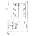
- FIG. 4 is a block diagram illustrating a hardware configuration example of the sensor node 102.
- FIG. 5 is an explanatory diagram illustrating an example of a premise operation of the sensor node 102.
- FIG. 6 is an explanatory diagram illustrating an example of a power state of each component.
- FIG. 7 is a block diagram illustrating a hardware configuration example of the server 201 and the parent device 101.
- FIG. 8 is an explanatory diagram showing a packet configuration example.
- FIG. 8 is an explanatory diagram showing a packet configuration example.
- FIG. 9 is an explanatory diagram illustrating a functional configuration example of the sensor node 102.
- FIG. 10 is an explanatory diagram illustrating a functional configuration example of the parent device 101.
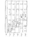
- FIG. 11 is an explanatory diagram illustrating an example of transmission / reception of the synchronization signal S2 and the synchronization request signal S1.
- FIG. 12 is an explanatory diagram illustrating a timing chart example regarding transmission / reception of the synchronization request signal S1 and the synchronization signal S2.
- FIG. 13 is a flowchart illustrating an example of a processing procedure performed by the sensor node 102 in a synchronization incomplete state.
- FIG. 14 is a flowchart illustrating an example of a processing procedure performed by the sensor node 102 in the synchronization request standby state.
- FIG. 15 is a flowchart illustrating an example of a processing procedure performed by the sensor node 102 in the synchronization completion state.
- FIG. 16 is a flowchart illustrating an example of a
- FIG. 1 is an explanatory diagram showing an operation example of the system according to the present invention.
- the system 100 is a sensor network system in which a sensor node 102 having a sensor and a small wireless communication circuit forms a sensor network SNET and collects sensor data.
- the system 100 includes a plurality of sensor nodes 102 and a parent device 101.
- the sensor node 102 is a wireless communication node having a sensor, and is provided in the arrangement area 103.
- sensor nodes 102-1 to 102-4 are provided in the arrangement area 103.
- the sensor node 102 charges a battery with electric power obtained by self-power generation.
- Base device 101 is a communication device for collecting sensor data from a plurality of sensor nodes 102.
- FIG. 100 A detailed example of the system 100 is shown in FIG.
- the state of the arrangement area 103 is measured using a plurality of sensor nodes 102 at predetermined time intervals. Examples of the measurement include temperature, humidity, pressure, and light. More specifically, measurement data and the like are transferred to the parent device 101 by performing multi-hop communication with a plurality of sensor nodes 102.
- each sensor is synchronized between the construction process and the synchronization.
- Node 102 must be up.
- the construction process is a process such as arranging the sensor node 102 in the arrangement area 103. In this case, the capacity of the battery mounted on each sensor node 102 increases.
- the power of each sensor node 102 may be turned on manually. For example, when the sensor node 102 is buried in the arrangement area 103, the power of each sensor node 102 cannot be turned on manually. For example, if the number of sensor nodes 102 is large, manual work is not realistic.
- each sensor node 102 receives the synchronization signal S2 by switching the reception unit from the off state to the on state and requesting the transmission of the synchronization signal S2, so that the reception unit is continuously connected.
- the period during which the device is in the on state can be shortened. Thereby, battery saving can be achieved.
- each sensor node 102 receives a first state from a first state where the power consumption of the receiving unit of the sensor node 102 is the first power when the capacity of the mounted battery exceeds a predetermined amount.
- the receiving unit is controlled to be in the second state, which is the second power higher than the power.
- the predetermined amount is determined by, for example, the designer of the sensor node 102. For example, the predetermined amount is 4/5 of the capacity of the battery.
- the first state is that the receiving unit is off, and the second state is that the receiving unit is on.
- the sensor node 102 transmits a synchronization request signal S1 for requesting transmission of a synchronization signal S2 for synchronizing multi-hop communication.
- the sensor node 102 receives the synchronization signal S2 with respect to the synchronization request signal S1.
- the sensor node 102-1 receives a synchronization signal S2 corresponding to the transmitted synchronization request signal S1 from the parent device 101 by the receiving unit.
- a specific configuration example of each of the synchronization signal S2 and the synchronization request signal S1 is illustrated in FIG.
- the sensor nodes 102-2 to 102-4 also transmit the synchronization request signal S1, but the synchronization request signal S1 does not reach the parent device 101.
- the sensor node 102 receives the synchronization request signal S1 so that the state of the reception unit becomes the first state when the reception unit does not receive the synchronization signal S2 until a certain period of time elapses after the transmission.
- the certain time is a value determined by, for example, a designer of the system 100 or a user of the system 100.
- the sensor node 102 when the sensor node 102 receives the synchronization request signal S1 from the other sensor node 102 after the receiving unit receives the synchronization signal S2, the sensor node 102 receives the synchronization signal S2 for the received synchronization request signal S1 and receives the synchronization request signal S1.
- a synchronization signal S2 is transmitted based on the synchronization signal S2.
- the sensor node 102-1 receives each synchronization request signal S1 transmitted from the sensor nodes 102-2 to 102-4.
- the sensor node 102-1 transmits a synchronization signal S2 corresponding to the received synchronization request signal S1, which is based on the synchronization signal S2 received from the parent device 101.
- the synchronization signal S2 can be received. Therefore, the amount of transmission power of the synchronization request signal S1 and the synchronization signal S2 may be small, so that power saving can be achieved.
- the sensor node 102 controls the receiving unit so that the state of the receiving unit becomes the first state after a predetermined time has elapsed since the receiving unit received the synchronization signal S2.
- the sensor node 102-1 is not already in a state capable of receiving the synchronization request signal S1.
- the sensor nodes 102-2 to 102-4 are in a state where they can receive the synchronization request signal S1.
- each sensor node 102 receives the synchronization signal S2 by switching the reception unit from the off state to the on state and requesting transmission of the synchronization signal S2, so that the reception unit is continuously turned on.
- the period can be shortened. Therefore, it is not necessary to maintain the reception operation by the receiving unit until that timing, as compared with the case where all the sensor nodes 102 deliver the synchronization signal S2 after the timing at which the synchronization signal S2 can be received. Further, as compared with the case where the synchronization signal S2 is delivered after the construction process is finished, the reception operation by the receiving unit may not be maintained until that timing. Therefore, battery saving can be achieved.
- FIG. 2 is an explanatory diagram showing an example of a system 100 according to the present invention.
- a change in the environment of the arrangement area 103 in which the sensor node 102 is provided is detected by collecting measurement values measured by a plurality of wireless sensor nodes 102, for example.
- the system 100 includes a server 201, a gateway 202, a parent device 101, and a plurality of sensor nodes 102.
- the server 201 and the gateway 202 are connected via a network NET such as the Internet.
- each device may be connected to a user terminal via a network NET.
- the server 201 collects, accumulates, and analyzes measurement values, and controls the entire system 100 such as the gateway 202, the parent device 101, and the sensor node 102.
- the gateway 202 relays signal exchange between the network NET to which the server 201 and the user terminal are connected, and the sensor network SNET by the plurality of sensor nodes 102 and the parent device 101.
- the parent device 101 collects measurement values by communicating with the sensor node 102 and notifies the server 201 of the collection results. Further, the parent device 101 may issue an instruction to the sensor node 102, for example.
- the plurality of sensor nodes 102 are communication nodes that measure the state of each position in the arrangement area 103. In addition, the plurality of sensor nodes 102 can communicate with surrounding sensor nodes 102 and the parent device 101 wirelessly.
- FIG. 3 is an explanatory diagram showing an operation example of the system 100.
- the state of the predetermined area is measured every predetermined time d.
- the system 100 causes the sensor node 102 to measure the state of a predetermined area once every 10 minutes, and collects the measurement data to the server through the parent device 101, the gateway 202, and the network. Therefore, in order to perform periodic measurement, each sensor node 102 must be synchronized.
- FIG. 4 is a block diagram illustrating a hardware configuration example of the sensor node 102.
- the sensor node 102 includes a sensor 401, an MCU (Micro Control Unit) 402, a timer 403, a ROM (Read Only Memory) 404, a RAM (Random Access Memory) 405, and a nonvolatile memory 406.
- the sensor node 102 includes a wireless circuit 408, an antenna 409, a power management unit 410, a battery 411, a harvester 412, and the like.
- the sensor node 102 includes an internal bus 407 that connects the sensor 401, MCU 402, timer 403, ROM 404, RAM 405, and nonvolatile memory 406. Further, in FIG. 4, a dotted line indicates a power supply line, and a solid line indicates a signal line.
- Sensor 401 detects a predetermined amount of displacement at the installation location.
- a piezoelectric element that detects a pressure at an installation location an element that detects temperature, a photoelectric element that detects light, or the like can be used.
- the MCU 402 is a control unit that performs overall control of the sensor node 102 and data processing, for example, by loading a program stored in the ROM 404 into the RAM 405 and executing the program.
- the MCU 402 processes data detected by the sensor 401.
- the timer 403 counts the time set by the MCU 402 or the like. In the present embodiment, for example, the timer 403 counts a sensing interval for sensing by the sensor 401 spontaneously. Further, for example, the timer 403 counts a predetermined period during which the short-range wireless circuit is stopped in the second embodiment to be described later.
- the ROM 404 is a storage unit that stores programs executed by the MCU 402.
- the RAM 405 is a storage unit that stores temporary data for processing in the MCU 402.
- the nonvolatile memory 406 is a writable memory, and is a storage unit that holds predetermined data that is written even when power supply is interrupted.
- the writable nonvolatile memory 406 includes a flash memory.
- the antenna 409 transmits and receives radio waves for wireless communication with other sensor nodes 102 and the gateway 202.
- the radio circuit 408 is RF (Radio Frequency).
- the radio circuit 408 includes a reception circuit 422 that outputs a radio wave received via the antenna 409 as a reception signal, and a transmission circuit 421 that transmits a transmission signal via the antenna 409 as a radio wave.
- the transmission power of the transmission circuit 421 can be switched by the MCU 402. The transmission power is determined based on the arrangement area 103 of the sensor node 102, the number of arrangement of the sensor nodes 102, the arrangement position of the parent device 101, and the like. In the present embodiment, for example, each transmission power of the transmission circuit 421 is set so that a signal can reach a predetermined distance.
- the harvester 412 generates power based on the external environment at the location where the sensor node 102 is installed, for example, energy changes such as light, vibration, temperature, and radio waves. In the example of FIG. 4, only one harvester 412 is provided. However, the present invention is not limited thereto, and a plurality of the same type of harvesters 412 may be provided, or a plurality of different types of harvesters 412 may be provided. Good.
- the harvester 412 may generate power according to the amount of displacement detected by the sensor 401, or may generate power according to the amount of displacement of the received radio wave received by the wireless circuit 408.
- the battery 411 stores the electric power generated by the harvester 412.
- the sensor node 102 is not provided with a primary battery, an external power source, or the like, and generates electric power required for operation inside the own device.
- the power management unit 410 performs control to supply the power stored by the battery 411 to each unit of the sensor node 102 as a driving power source.
- FIG. 5 is an explanatory diagram showing an example of a premise operation of the sensor node 102.
- each sensor node 102 performs an intermittent operation. In the intermittent operation, each sensor node 102 switches from a sleep state described later to an activation state described later every predetermined time d. The predetermined time d is determined by the user. And each sensor node 102 measures the state of an arrangement
- each sensor node 102 the remaining amount of the battery 411 is reduced by processing by the MCU 402, wireless transmission by the transmission circuit 421, reception by the reception circuit 422, etc. in the activated state.
- the remaining amount of the battery 411 increases due to charging in a sleep state described later.
- the plurality of sensor nodes 102 use multi-hop communication for data signals for notifying the base unit 101 of measured values of the sensors 401 included in each sensor node 102. Relay transfer. Further, as described above, each sensor node 102 sets the transmission power of the transmission circuit 421 as the first transmission power in the activated state.
- FIG. 6 is an explanatory diagram showing an example of the power state of each component.
- the power state of the MCU 402 includes an on state, a sleep state, and an off state.
- the ON state is a state in which voltages that can be processed by the MCU 402 are supplied to the MCU 402.
- the sleep state is a state in which power is supplied to an interrupt circuit or the like included in the MCU 402 or the timer 403, and power is not supplied to a circuit or the like having a main function such as an operation of the MCU 402.
- the interrupt circuit included in the MCU 402 receives an interrupt signal, the MCU 402 is turned on.
- the off state is a state in which power is not supplied to all of the MCU 402 and any operation cannot be performed, but the off state is not used in this embodiment.
- the power state of the receiving circuit 422 includes an off state that is a first state and an off state that is a second state.
- the on state is a state where power is supplied to the receiving circuit 422.
- the off state is a state in which power is not supplied to the reception circuit 422 and a state in which radio waves cannot be received.
- the power state of the sensor 401 includes an on state and an off state.
- the on state is a state where power is supplied to the sensor 401.
- the off state is a state in which power is not supplied to the sensor 401.
- the MCU 402 when the sensor node 102 is in the activated state, the MCU 402 is in the on state, the receiving circuit 422 is in the on state, and the sensor 401 is in the on state.
- the MCU 402 when the sensor node 102 is in the sleep state, the MCU 402 is in the sleep state, the reception circuit 422 is in the off state, and the sensor 401 is in the off state.
- FIG. 7 is a block diagram illustrating a hardware configuration example of the server 201 and the parent device 101. Since the server 201 and the parent device 101 may have the same configuration, the server 201 and the parent device 101 will be described as the same configuration. In order to indicate either the server 201 or the parent device 101, in FIG.
- the device 700 operates based on an external power supply.
- the apparatus 700 includes a CPU (Central Processing Unit) 701, a timer 702, a ROM 703, a RAM 704, a disk drive 705, a disk 706, and an I / O (Input / Output) circuit 707.
- the apparatus 700 includes an internal bus 711 that connects a CPU 701, a timer 702, a ROM 703, a RAM 704, a disk drive 705, and an I / O circuit 707.
- the CPU 701 is a control unit that controls the entire apparatus 700.
- the ROM 703 is a storage unit that stores programs such as a boot program.
- a RAM 704 is a storage unit used as a work area for the CPU 701.
- the disk drive 705 controls reading / writing of data with respect to the disk 706 according to the control of the CPU 701.
- the disk 706 is a storage unit that stores data written under the control of the disk drive 705. Examples of the disk 706 include a magnetic disk and an optical disk.
- the storage unit such as the ROM 703 and the disk 706 stores predetermined time information described later and standby time information described later.
- a radio communication circuit 708 and an antenna 709 are connected to the I / O circuit 707.
- wireless communication with the parent device 101 can be performed by wireless communication with the gateway 202 via the wireless communication circuit 708 and the antenna 709.
- wireless communication can be performed with the sensor node 102 via the wireless communication circuit 708 and the antenna 709.
- a network I / F 710 is connected to the I / O circuit 707.
- the device 700 can communicate with an external device via a network such as the Internet through a network I / F 710 by TCP (Transmission Control Protocol) / IP (Internet Protocol) protocol processing.
- TCP Transmission Control Protocol
- IP Internet Protocol
- wired communication or wireless communication can be applied to communication by the network I / F 710.
- the device 700 may be provided with an input device such as a keyboard, a mouse, or a touch panel. As a result, the user can directly operate the device 700 via the input device. Further, for example, an output device such as a display, a printer, or a buzzer may be provided in the device 700.
- an input device such as a keyboard, a mouse, or a touch panel.
- an output device such as a display, a printer, or a buzzer may be provided in the device 700.
- FIG. 8 is an explanatory diagram showing a packet configuration example.
- the synchronization request signal S1 is a signal for requesting synchronization from the sensor node 102 to the base unit 101 or the synchronized sensor node 102 after each of the sensor nodes 102 is installed in a predetermined area.
- the synchronization request signal S1 has an identification flag and a transmission source ID.
- the identification flag is a flag for identifying the synchronization request signal S1, and is, for example, “0x01”.
- the transmission source ID is identification information indicating the transmission source of the synchronization request signal S1.
- the synchronization signal S2 is a signal transmitted from the parent device 101 or the synchronized sensor node 102 to the sensor node 102 that is the transmission source of the synchronization request signal S1, and is a signal that notifies the synchronization timing.
- the synchronization signal S2 includes an identification flag, a destination ID, a transmission source ID, predetermined time information ddata indicating a predetermined time d, timing information indicating the next activation timing, and standby time information indicating a synchronization request standby time.
- the identification flag is a flag for identifying the synchronization signal S2, for example, “0x10”.
- the transmission source ID is identification information indicating the transmission source of the synchronization signal S2.
- the predetermined time information ddata is information indicating a time that is a measurement interval, for example.
- the timing information is information indicating the timing at which the MCU 402 and the sensor 401 are activated next time for measurement. For example, it may be information such as how many minutes later, or information indicating a specific time.
- the standby time information is information indicating a time for waiting for a synchronization request from another sensor node 102 after the synchronization is completed. For example, it may be information such as how many minutes later, or information indicating a specific time.
- FIG. 9 is an explanatory diagram illustrating a functional configuration example of the sensor node 102.
- the sensor node 102 includes an overall control unit 901, a reception unit 902, a transmission unit 903, a power control unit 904, a power storage unit 905, and a storage unit 906.
- the receiving unit 902 is realized by the receiving circuit 422.
- the transmission unit 903 is realized by the transmission circuit 421.
- the power control unit 904 is realized by the power management unit 410.
- the storage unit 906 is realized by the ROM 404, the RAM 405, the nonvolatile memory 406, etc. shown in FIG.
- the overall control unit 901 is realized by, for example, the MCU 402 and the timer 403 shown in FIG.
- Each process of the overall control unit 901 is coded in a program stored in the storage unit 906 accessible by the MCU 402 illustrated in FIG. 4, for example. Then, the MCU 402 reads the program from the storage unit 906 and executes the process coded in the program. Thereby, each process of the overall control unit 901 is realized. Further, the processing result of each unit is stored in the storage unit 906, for example.
- the power storage unit 905 has a function of voluntarily storing power supplied to each unit.
- the power storage unit 905 is, for example, the battery 411 illustrated in FIG.
- FIG. 10 is an explanatory diagram illustrating a functional configuration example of the parent device 101.
- Base device 101 includes a control unit 1001, a reception unit 1002, a transmission unit 1003, and a storage unit 1004.
- the storage unit 1004 is realized by, for example, the ROM 703, the RAM 704, the disk 706, etc. shown in FIG.
- the reception unit 1002 and the transmission unit 1003 are realized by, for example, the wireless communication circuit 708 illustrated in FIG.
- the control unit 1001 is realized by the CPU 701 shown in FIG.
- Each process of the control unit 1001 is coded in a program stored in the storage unit 1004 accessible by the CPU 701, for example.
- the CPU 701 reads the program from the storage unit 1004 and executes the process coded in the program. Thereby, each process of the control unit 1001 is realized.
- the processing result of each unit is stored in the storage unit 1004, for example.
- the overall control unit 901 illustrated in FIG. 9 controls the transmission unit 903 to transmit the synchronization request signal S1 when the amount of power stored in the power storage unit 905 exceeds a predetermined amount. For example, when receiving an interrupt such as completion of charging, the overall control unit 901 causes the power control unit 904 to switch the state of the sensor node 102 from the sleep state to the activated state. As described above, in the sleep state of the sensor node 102, the MCU 402 is in the sleep state, the sensor 401 and the reception circuit 422 are in the off state, and the timer 403 is activated.
- the MCU 402 since the MCU 402 is in the sleep state and can operate with respect to the interrupt function, it can accept an interrupt from the timer 403, the power management unit 410, or the like. In the activated state of the sensor node 102, the sensor 401, the MCU 402, and the reception circuit 422 are turned on.
- the overall control unit 901 generates a synchronization request signal S1.
- the transmission unit 903 transmits the synchronization request signal S1 generated by the overall control unit 901.
- the reception unit 902 receives the synchronization signal S2 corresponding to the synchronization request signal S1 transmitted by the transmission unit 903.
- the receiving unit 1002 illustrated in FIG. 10 receives the synchronization request signal S1 transmitted from the transmitting unit 903 illustrated in FIG. Then, the control unit 1001 illustrated in FIG. 10 generates a synchronization signal S2 for the synchronization request signal S1 received by the reception unit 1002.
- the transmission unit 1003 transmits the synchronization signal S2 generated by the control unit 1001.
- a detailed example of the generation of the synchronization signal S2 is shown in FIG.
- the synchronization signal S2 corresponding to the synchronization request signal S1 is a signal whose destination ID included in the synchronization signal S2 indicates the self-sensor node 102.
- 9 controls the storage unit 906 to store the predetermined time information ddata included in the synchronization signal S2 received by the receiving unit 902.
- the overall control unit 901 is based on the received synchronization signal S2 with respect to the received synchronization request signal S1 when receiving the synchronization request signal S1 from another sensor node 102 after the receiving unit 902 receives the synchronization signal S2. Control is performed to cause the transmission unit 903 to transmit the synchronization signal S2.
- the power control unit 904 controls the reception unit 902 so that the state of the reception unit 902 becomes the first state after a predetermined time has elapsed since the reception unit 902 received the synchronization signal S2.
- the fixed time here is, for example, the standby time indicated by the standby time information stdata included in the synchronization signal S2.
- the standby time is counted by the timer 403, for example.
- the overall control unit 901 sets the timing indicated by the timing information included in the synchronization signal S2 received by the receiving unit 902 in the timer 403. For example, the overall control unit 901 causes the power control unit 904 to switch the state of the sensor node 102 from the activated state to the sleep state. As a result, the timer 403 is interrupted at the next synchronization timing.
- the power control unit 904 determines that the state of the receiving unit 902 is the first state.
- the receiving unit 902 is controlled so as to be in a state.
- the certain time here is, for example, a value determined in advance by a designer or a user.
- information indicating the predetermined time is stored in advance in the storage unit 906 or the like.
- the fixed time is counted by the timer 403.
- the first state of the receiving unit 902 is an off state.
- the power control unit 904 changes the state of the sensor node 102 when the receiving unit 902 does not receive the synchronization signal S2 after the transmission unit 903 transmits the synchronization request signal S1 and after a predetermined time has elapsed. You may be in a sleep state.
- the overall control unit 901 performs synchronization based on the received synchronization signal S2 with respect to the received synchronization request signal S1. Control is performed to cause the transmission unit 903 to transmit the signal S2.
- the power control unit 904 determines that the state of the receiving unit 902 is the first state.
- the receiving unit 902 is controlled so as to be in a state.
- the overall control unit 901 controls the power control unit 904 to switch the state of the sensor node 102 from the sleep state to the activated state.
- the overall control unit 901 performs control to cause the sensor 401 to measure the state of the installation location.
- the overall control unit 901 performs control to cause the transmission unit 903 to transmit a data signal including the measurement result.
- the overall control unit 901 performs control to transfer the data signal received by the transmission unit 903 when the reception unit 902 receives a data signal from the sensor node 102 other than the own sensor node 102.
- the overall control unit 901 performs control to cause the power control unit 904 to switch the state of the sensor node 102 from the activated state to the sleep state.
- FIG. 11 is an explanatory diagram showing an example of transmission / reception of the synchronization signal S2 and the synchronization request signal S1.
- the sensor node 102-1 to the sensor node 102-10 are installed in the predetermined area. For example, each sensor node 102 transmits the synchronization signal S2 when charging is completed.
- base unit 101 receives synchronization request signal S1 transmitted from sensor node 102-1.
- the distance between the parent device 101 and the sensor nodes 102-2 to 102-10 is longer than the reachable distance depending on the transmission intensity of the synchronization request signal S1. Therefore, each synchronization request signal S1 transmitted from the sensor node 102-2 to sensor node 102-10 does not reach the parent device 101.
- base unit 101 transmits synchronization signal S2 addressed to sensor node 102-1 that is the transmission source of received synchronization request signal S1.
- the sensor node 102-1 When the sensor node 102-1 receives the synchronization signal S2 transmitted from the parent device 101, the sensor node 102-1 stores the predetermined time d designated by the synchronization signal S2 in the nonvolatile memory 406. Then, the sensor node 102-1 sets the timer 403 so as to be started after the next start timing specified by the synchronization signal S2. In addition, the sensor node 102-1 sets the standby time specified by the synchronization signal S2 in the timer 403, so that the synchronization request signal S1 is output between the reception of the synchronization signal S2 and the standby time. I wait.
- the sensor node 102-1 receives the synchronization request signal S1 from each of the sensor nodes 102-2 to 102-4, and then receives the synchronization request signal S1 from each of the sensor nodes 102-2 to 102-4.
- the synchronization signal S2 is transmitted.
- the sensor node 102-1 shifts to the sleep state.
- the sensor nodes 102-2 to 102-4 store in the nonvolatile memory 406 a predetermined time d specified by the synchronization signal S2. Then, the sensor nodes 102-2 to 102-4 set the timer 403 so as to start after the next start timing specified by the synchronization signal S2.
- the sensor nodes 102-2 to 102-4 set the standby time designated by the synchronization signal S2 in the timer 403 so that the standby time elapses from the reception of the synchronization signal S2. Then, it waits for the synchronization request signal S1.
- the sensor node 102-2 upon receiving the synchronization request signal S1 transmitted from the sensor node 102-6, the sensor node 102-2 transmits the synchronization signal S2 to the sensor node 102-6.
- the sensor node 102-2 shifts to the sleep state.
- the sensor node 102-6 receives the synchronization signal S2 from the sensor node 102-2, the sensor node 102-6 stores the predetermined time d designated by the synchronization signal S2 in the nonvolatile memory 406. Then, the sensor node 102-6 sets the timer 403 to start after the next start timing specified by the synchronization signal S2.
- the sensor node 102-6 sets the standby time designated by the synchronization signal S2 in the timer 403, so that the synchronization request signal S1 is output between the reception of the synchronization signal S2 and the standby time. I wait.
- the sensor node 102-3 when the sensor node 102-3 receives the synchronization request signal S1 transmitted from the sensor node 102-7, the sensor node 102-3 transmits the synchronization signal S2 to the sensor node 102-7.
- the sensor node 102-7 When the standby time elapses, the sensor node 102-3 transitions to the sleep state.
- the sensor node 102-7 receives the synchronization signal S2 from the sensor node 102-3, the sensor node 102-7 stores the predetermined time d designated by the synchronization signal S2 in the nonvolatile memory 406. Then, the sensor node 102-7 sets the timer 403 so as to be started after the next start timing designated by the synchronization signal S2.
- the sensor node 102-7 sets the standby time designated by the synchronization signal S2 in the timer 403, so that the synchronization request signal S1 is output between the reception of the synchronization signal S2 and the standby time. I wait.
- the sensor node 102-4 when the sensor node 102-4 receives the synchronization request signal S1 transmitted from each of the sensor node 102-5 and the sensor node 102-8, the sensor node 102-5 and the sensor node 102- 8 transmits a synchronization signal S2.
- the sensor node 102-4 shifts to the sleep state.
- the sensor node 102-5 and the sensor node 102-8 receive the synchronization signal S2 from the sensor node 102-4, the predetermined time d designated by the synchronization signal S2 is stored in the nonvolatile memory 406.
- the sensor node 102-5 and the sensor node 102-8 set the timer 403 so as to start after the next start timing designated by the synchronization signal S2. Further, the sensor node 102-5 and the sensor node 102-8 set the standby time specified by the synchronization signal S2 in the timer 403, so that the standby time elapses from the reception of the synchronization signal S2. Then, it waits for the synchronization request signal S1.
- the sensor node 102-7 when the sensor node 102-7 receives the synchronization request signal S1 transmitted from the sensor node 102-9, the sensor node 102-7 transmits a synchronization signal S2 to the sensor node 102-9.
- the sensor node 102-9 shifts to the sleep state.
- the sensor node 102-9 receives the synchronization signal S2 from the sensor node 102-7, the sensor node 102-9 stores the predetermined time d specified by the synchronization signal S2 in the nonvolatile memory 406. Then, the sensor node 102-9 sets the timer 403 so as to be started after the next start timing specified by the synchronization signal S2.
- the sensor node 102-9 sets the standby time designated by the synchronization signal S2 in the timer 403, so that the synchronization request signal S1 is received between the reception of the synchronization signal S2 and the standby time. I wait.
- the sensor node 102-8 when the sensor node 102-8 receives the synchronization request signal S1 transmitted from the sensor node 102-10, the sensor node 102-8 transmits a synchronization signal S2 to the sensor node 102-10.
- the sensor node 102-8 shifts to the sleep state.
- the sensor node 102-10 receives the synchronization signal S2 from the sensor node 102-8, the sensor node 102-10 stores the predetermined time d specified by the synchronization signal S2 in the nonvolatile memory 406. Then, the sensor node 102-10 sets the timer 403 to start after the next start timing specified by the synchronization signal S2.
- the sensor node 102-10 sets the standby time specified by the synchronization signal S2 in the timer 403, so that the synchronization request signal S1 is output between the reception of the synchronization signal S2 and the standby time. I wait.
- the sensor node 102-9 and the sensor node 102-10 wait for the synchronization request signal S1, but since neither of the sensor nodes 102 has completed the synchronization, the synchronization signal S2 is not received.
- the sensor node 102-9 and the sensor node 102-10 shift to the sleep state when the standby time has elapsed.
- each sensor node 102 performs measurement every predetermined time d as described above, and transfers measurement data to the parent device 101 by relay transfer such as multi-hop communication as described above.
- FIG. 12 is an explanatory diagram showing an example of a timing chart regarding transmission / reception of the synchronization request signal S1 and the synchronization signal S2.
- the sensor node 102-1 transmits the synchronization request signal S1
- the sensor node 102-1 receives the synchronization signal S2 from the parent device 101.
- the sensor node 102-1 waits for the synchronization request signal S1. Thereafter, when the standby time st elapses, the sensor node 102-1 performs measurement by the sensor 401 every predetermined time d.
- the sensor node 102-2 transmits the synchronization request signal S1
- the sensor node 102-2 receives the synchronization signal S2 from the parent device 101. Then, the sensor node 102-2 waits for the synchronization request signal S1. Thereafter, when the standby time st elapses, the sensor node 102-2 performs measurement by the sensor 401 every predetermined time d.
- the sensor node 102-3 transmits the synchronization request signal S1
- the sensor node 102-3 receives the synchronization signal S2 from the parent device 101.
- the sensor node 102-3 waits for the synchronization request signal S1.
- the sensor node 102-4 and the sensor node 102-5 transmit the synchronization request signal S1
- the sensor node 102-4 receives the synchronization signal S2 from the sensor node 102-3.
- the standby time st elapses
- the sensor node 102-3 performs measurement by the sensor 401 every predetermined time d.
- the sensor node 102-4 and the sensor node 102-5 wait for the synchronization request signal S1. Thereafter, when the standby time st elapses, the sensor node 102-4 and the sensor node 102-5 perform measurement by the sensor 401 every predetermined time d.
- FIG. 13 is a flowchart illustrating an example of a processing procedure performed by the sensor node 102 in a synchronization incomplete state.
- the sensor node 102 switches from the sleep state to the activated state upon completion of charging or the like (step S1301).
- the sensor node 102 transmits a synchronization request signal S1 (step S1302).
- the completion of charging is notified by transmitting an interrupt signal from the power management unit 410 or the like to the MCU 402.
- the sensor node 102 determines whether or not the synchronization signal S2 has been received (step S1303).
- the sensor node 102 stores the predetermined time d in the nonvolatile memory 406 (step S1304). Then, the sensor node 102 sets an interrupt to the timer 403 so as to start after the next start timing (step S1305). Next, the sensor node 102 waits for a standby time for a synchronization request (step S1306), and proceeds to step S1307.
- the processing procedure performed by the sensor node 102 in the standby state for the synchronization request is shown in FIG.
- Step S1303 If it is determined that the synchronization signal S2 has not been received between the time when the synchronization request signal S1 is transmitted and the elapse of a certain time (step S1303: No), the sensor node 102 switches from the activated state to the sleep state. (Step S1307), a series of processing ends. As described above, in this sleep state, the MCU 402 is in the sleep state, the sensor 401 and the reception circuit 422 are in the off state, and the timer 403 is activated. Here, since the MCU 402 is in the sleep state and can operate with respect to the interrupt function, it can accept an interrupt from the timer 403 or the like.
- FIG. 14 is a flowchart illustrating an example of a processing procedure performed by the sensor node 102 in the synchronization request standby state.
- the sensor node 102 acquires the current time from the timer 403, triggered by the reception of the synchronization request signal S1 (step S1401).
- the sensor node 102 acquires the next activation scheduled time (step S1402).
- the sensor node 102 obtains the next activation timing by subtracting the current time from the next activation scheduled time (step S1403).
- the sensor node 102 transmits the synchronization signal S2 (step S1404), and ends the series of processes.
- FIG. 15 is a flowchart illustrating an example of a processing procedure performed by the sensor node 102 in the synchronization completion state.
- the sensor node 102 switches to an activated state in response to an interrupt from the timer 403 (step S1501).
- the sensor node 102 sets an interrupt to the timer so as to start after a predetermined time d (step S1502).
- the sensor node 102 performs regular measurement (step S1503).
- the sensor node 102 switches to the sleep state (step S1504) and ends the series of processes.
- the MCU 402 is in the sleep state
- the sensor 401 and the reception circuit 422 are in the off state
- the timer 403 is activated.
- the MCU 402 since the MCU 402 is in the sleep state and can operate with respect to the interrupt function, it can accept an interrupt from the timer 403 or the like.
- FIG. 16 is a flowchart illustrating an example of a processing procedure performed by the parent device 101.
- base unit 101 receives the synchronization request signal S1 as a trigger and acquires the current time from the timer (step S1601).
- Master device 101 obtains a remainder obtained by dividing the current time by predetermined time d (step S1602).
- Master device 101 obtains the next activation timing by subtracting the calculated remainder from predetermined time d (step S1603).
- Master device 101 transmits synchronization signal S2 (step S1604), and the series of processing ends.
- each of the sensor nodes 102 receives the synchronization signal by switching the reception circuit from the off state to the on state and requesting the transmission of the synchronization signal, so that the reception circuit is continuously turned on.
- the period can be shortened. Thereby, battery saving can be achieved.
- the sensor node 102 when the sensor node 102 receives a synchronization request signal from another sensor node 102 after receiving the synchronization signal, the sensor node 102 transmits a synchronization signal based on the received synchronization signal with respect to the received synchronization request signal. In this way, when the sensor node 102 that has completed synchronization transmits a synchronization signal on behalf of the parent device, each sensor node 102 transmits a synchronization request signal with transmission power that can reach the parent device. Thus, power saving can be achieved.
- the sensor node 102 switches the receiving circuit to an off state after a certain time has elapsed after receiving the synchronization signal.
- power saving is achieved by performing an intermittent operation after completing the transmission of the synchronization signal in response to the synchronization request signal from the other sensor node 102 at a short distance.
- the sensor node 102 transmits a synchronization request signal when the amount of power stored in the battery exceeds a predetermined amount.
- the synchronization request signal and the synchronization signal can be transmitted and received at a spontaneous timing. Therefore, battery saving can be achieved.
- the sensor node 102 controls the receiving unit to be in the first state. Therefore, since intermittent operation is realized, battery saving can be achieved.
- multi-hop communication is performed periodically. Thereby, the state of the arrangement area is regularly measured.
- the synchronization method described in this embodiment can be realized by executing a synchronization program prepared in advance by the MCU 402.
- the synchronization program is recorded on a recording medium readable by the MCU 402 such as the ROM 404 and the nonvolatile memory 406, and is executed by being read from the recording medium by the MCU 402. Further, the synchronization program may be distributed from the parent device 101 by multi-hop communication.
- SYMBOLS 100 System 101 Base machine 102 Sensor node 401 Sensor 402 MCU 403 Timer 404 ROM 405 RAM 406 Non-volatile memory 410 Power management unit 411 Battery 421 Transmission circuit 422 Reception circuit 701 CPU 702 Timer 703 ROM 704 RAM 706 Disk 901 Overall control unit 902 Reception unit 903 Transmission unit 904 Power control unit 905 Power storage unit 1001 Control unit 1002 Reception unit 1003 Transmission unit 1004 Storage unit S1 Synchronization request signal S2 Synchronization signal
Landscapes
- Engineering & Computer Science (AREA)
- Computer Networks & Wireless Communication (AREA)
- Signal Processing (AREA)
- Mobile Radio Communication Systems (AREA)
- Arrangements For Transmission Of Measured Signals (AREA)
Abstract
Description
図4は、センサノード102のハードウェア構成例を示すブロック図である。センサノード102は、センサ401と、MCU(Micro Control Unit)402と、タイマ403と、ROM(Read Only Memory)404と、RAM(Random Access Memory)405と、不揮発メモリ406と、を有する。また、センサノード102は、無線回路408と、アンテナ409と、電源管理ユニット410と、バッテリ411と、ハーベスタ412と、などを有する。また、センサノード102は、センサ401と、MCU402と、タイマ403と、ROM404と、RAM405と、不揮発メモリ406と、を接続する内部バス407を有する。また、図4中、点線は電源線を示し、実線は信号線を示す。
図7は、サーバ201および親機101のハードウェア構成例を示すブロック図である。サーバ201と親機101とは、同様の構成であってもよいため、同一構成として説明するが、これに限らず、異なる構成であってもよい。サーバ201と親機101とのいずれかを指すために、図7では、単に装置700と称する。
図9は、センサノード102の機能的構成例を示す説明図である。センサノード102は、全体制御部901と、受信部902と、送信部903と、電力制御部904と、蓄電部905と、記憶部906と、を有する。受信部902は、受信回路422によって実現される。送信部903は、送信回路421によって実現される。電力制御部904は、電源管理ユニット410によって実現される。記憶部906は、例えば、図4に示したROM404やRAM405や不揮発メモリ406などによって実現される。全体制御部901は、例えば、図4に示したMCU402やタイマ403などによって実現される。また、全体制御部901の各処理は、例えば、図4に示したMCU402がアクセス可能な記憶部906に記憶されたプログラムにコーディングされている。そして、MCU402が記憶部906からプログラムを読み出して、プログラムにコーディングされている処理を実行する。これにより、全体制御部901の各処理が実現される。また、各部の処理結果は、例えば、記憶部906に記憶される。蓄電部905は、各部に供給される電力を自発的に蓄電する機能を有する。蓄電部905は、例えば、図4に示したバッテリ411である。
図10は、親機101の機能的構成例を示す説明図である。親機101は、制御部1001と、受信部1002と、送信部1003と、記憶部1004と、を有する。記憶部1004は、例えば、図7に示したROM703、RAM704、ディスク706などによって実現される。受信部1002および送信部1003は、例えば、図7に示した無線通信回路708によって実現される。制御部1001は、図7に示したCPU701などによって実現される。また、制御部1001の各処理は、例えば、CPU701がアクセス可能な記憶部1004に記憶されたプログラムにコーディングされている。そして、CPU701が記憶部1004からプログラムを読み出して、プログラムにコーディングされている処理を実行する。これにより、制御部1001の各処理が実現される。また、各部の処理結果は、例えば、記憶部1004に記憶される。
図13は、同期未完状態においてセンサノード102が行う処理手順例を示すフローチャートである。センサノード102は、充電完了などを契機として、スリープ状態から起動状態に切り替える(ステップS1301)。つぎに、センサノード102は、同期要求信号S1を送信する(ステップS1302)。例えば、充電完了などは、電源管理ユニット410などからMCU402へ割り込み信号が送信されることによって通知される。センサノード102は、同期信号S2を受信したか否かを判断する(ステップS1303)。
図16は、親機101が行う処理手順例を示すフローチャートである。まず、親機101は、同期要求信号S1の受信を契機として、タイマから現在時刻を取得する(ステップS1601)。親機101は、現在時刻を所定時間dで割った余りを求める(ステップS1602)。親機101は、所定時間dから、算出した余りを引くことにより、次回起動タイミングを求める(ステップS1603)。親機101は、同期信号S2を送信し(ステップS1604)、一連の処理を終了する。
101 親機
102 センサノード
401 センサ
402 MCU
403 タイマ
404 ROM
405 RAM
406 不揮発メモリ
410 電源管理ユニット
411 バッテリ
421 送信回路
422 受信回路
701 CPU
702 タイマ
703 ROM
704 RAM
706 ディスク
901 全体制御部
902 受信部
903 送信部
904 電力制御部
905 蓄電部
1001 制御部
1002 受信部
1003 送信部
1004 記憶部
S1 同期要求信号
S2 同期信号
Claims (9)
- マルチホップ通信によってデータを通信装置へ転送する複数の通信ノードに含まれる通信ノードであって、
自通信ノードにおいて前記マルチホップ通信の同期を取るための同期信号の送信を要求する同期要求信号を送信する送信部と、
前記送信部が送信した前記同期要求信号に対する前記同期信号を受信する受信部と、
前記受信部の状態が、前記送信部が前記同期要求信号を送信する前には前記受信部の消費電力が第1電力である第1状態となり、前記送信部が前記同期要求信号を送信した後には前記受信部の消費電力が前記第1電力よりも高い第2電力である第2状態となるように前記受信部を制御する電力制御部と、
を有することを特徴とする通信ノード。 - 前記受信部が前記同期信号を受信した後に前記複数の通信ノードのうちの自通信ノード以外の通信ノードからの前記同期要求信号を受信した場合に、前記受信部が受信した前記同期要求信号に対する、受信した前記同期信号に基づく前記同期信号を、前記送信部に送信させる制御を行う送信制御部を有することを特徴とする請求項1に記載の通信ノード。
- 前記電力制御部は、前記受信部が前記同期信号を受信してから一定時間経過後に、前記受信部の状態が前記第1状態となるように前記受信部を制御することを特徴とする請求項2に記載の通信ノード。
- 前記受信部に供給される電力を蓄電する蓄電部を有し、
前記送信制御部は、前記蓄電部に蓄電された電力量が所定量以上になった場合に、前記同期要求信号を前記送信部に送信させるように制御することを特徴とする請求項2または3に記載の通信ノード。 - 前記電力制御部は、前記送信部が前記同期要求信号を送信してから一定時間経過後までに、前記受信部が前記同期信号を受信しなかった場合、前記受信部の状態が前記第1状態となるように前記受信部を制御することを特徴とする請求項4に記載の通信ノード。
- 前記マルチホップ通信は周期的に行われることを特徴とする請求項1~5のいずれか一つに記載の通信ノード。
- 通信装置と、
マルチホップ通信によってデータを前記通信装置へ転送する複数の通信ノードと、
を有するシステムであって、
前記複数の通信ノードに含まれる通信ノードが、
受信部の状態を、前記受信部の消費電力が第1電力である第1状態から前記受信部の消費電力が前記第1電力よりも高い第2電力である第2状態に切り替え、
自通信ノードにおいて前記マルチホップ通信の同期を取るための同期信号の送信を要求する同期要求信号を送信部によって送信し、
前記送信部が送信した前記同期要求信号に対する前記同期信号を前記受信部によって受信することを特徴とするシステム。 - 前記通信装置は、
前記複数の通信ノードのうちいずれかの通信ノードから送信された前記同期要求信号を受信すると、受信した前記同期要求信号に対する同期信号を送信することを特徴とする請求項7に記載のシステム。 - マルチホップ通信によってデータを通信装置へ転送する複数の通信ノードに含まれる通信ノードが、
受信部の状態を、前記受信部の消費電力が第1電力である第1状態から前記受信部の消費電力が前記第1電力よりも高い第2電力である第2状態に切り替え、
自通信ノードにおいて前記マルチホップ通信の同期を取るための同期信号の送信を要求する同期要求信号を送信部によって送信し、
前記送信部が送信した前記同期要求信号に対する前記同期信号を前記受信部によって受信する、
処理を実行することを特徴とする同期方法。
Priority Applications (6)
| Application Number | Priority Date | Filing Date | Title |
|---|---|---|---|
| JP2015557667A JP6197881B2 (ja) | 2014-01-20 | 2014-01-20 | 通信ノード、システム、および同期方法 |
| CN201480073376.3A CN105917683A (zh) | 2014-01-20 | 2014-01-20 | 通信节点、系统以及同步方法 |
| PCT/JP2014/050929 WO2015107689A1 (ja) | 2014-01-20 | 2014-01-20 | 通信ノード、システム、および同期方法 |
| GB1611986.9A GB2536178B (en) | 2014-01-20 | 2014-01-20 | Communications node, system, and synchronizing method |
| TW103146021A TWI549554B (zh) | 2014-01-20 | 2014-12-29 | 通信節點、通信系統,及同步方法 |
| US15/204,233 US10091748B2 (en) | 2014-01-20 | 2016-07-07 | Communications node, system, and synchronizing method |
Applications Claiming Priority (1)
| Application Number | Priority Date | Filing Date | Title |
|---|---|---|---|
| PCT/JP2014/050929 WO2015107689A1 (ja) | 2014-01-20 | 2014-01-20 | 通信ノード、システム、および同期方法 |
Related Child Applications (1)
| Application Number | Title | Priority Date | Filing Date |
|---|---|---|---|
| US15/204,233 Continuation US10091748B2 (en) | 2014-01-20 | 2016-07-07 | Communications node, system, and synchronizing method |
Publications (1)
| Publication Number | Publication Date |
|---|---|
| WO2015107689A1 true WO2015107689A1 (ja) | 2015-07-23 |
Family
ID=53542607
Family Applications (1)
| Application Number | Title | Priority Date | Filing Date |
|---|---|---|---|
| PCT/JP2014/050929 Ceased WO2015107689A1 (ja) | 2014-01-20 | 2014-01-20 | 通信ノード、システム、および同期方法 |
Country Status (6)
| Country | Link |
|---|---|
| US (1) | US10091748B2 (ja) |
| JP (1) | JP6197881B2 (ja) |
| CN (1) | CN105917683A (ja) |
| GB (1) | GB2536178B (ja) |
| TW (1) | TWI549554B (ja) |
| WO (1) | WO2015107689A1 (ja) |
Cited By (3)
| Publication number | Priority date | Publication date | Assignee | Title |
|---|---|---|---|---|
| WO2018083806A1 (ja) * | 2016-11-07 | 2018-05-11 | 富士通株式会社 | 制御装置、制御システム及び制御方法 |
| WO2021044557A1 (ja) * | 2019-09-04 | 2021-03-11 | 三菱電機株式会社 | 無線通信装置、制御回路、記憶媒体および無線通信方法 |
| JP2021535635A (ja) * | 2018-08-27 | 2021-12-16 | グーグル エルエルシーGoogle LLC | メッシュネットワークにおける同期受信 |
Families Citing this family (18)
| Publication number | Priority date | Publication date | Assignee | Title |
|---|---|---|---|---|
| WO2015120463A1 (en) * | 2014-02-10 | 2015-08-13 | Big Belly Solar, Inc. | Dynamically adjustable nodes in a sensor network |
| US10285131B2 (en) | 2014-08-14 | 2019-05-07 | Big Belly Solar, Inc. | Dynamically adjustable nodes in a sensor network |
| TWI588507B (zh) * | 2015-10-14 | 2017-06-21 | 國立成功大學 | 具定位功能之射頻傳能裝置及射頻能量獵能裝置及具定位功能之射頻傳能方法 |
| US10560973B2 (en) * | 2016-02-18 | 2020-02-11 | Panasonic Intellectual Property Management Co., Ltd. | Terminal device, terminal device control method, and wireless communication system using said terminal device |
| WO2018081795A1 (en) | 2016-10-31 | 2018-05-03 | Zipline Medical, Inc. | Systems and methods for monitoring physical therapy of the knee and other joints |
| TWI633710B (zh) * | 2017-01-17 | 2018-08-21 | 台達電子工業股份有限公司 | 具極化追蹤之射頻傳能裝置、具定位與極化追蹤之射頻傳能裝置、射頻獵能裝置及其射頻傳能方法 |
| GB2574074B (en) | 2018-07-27 | 2020-05-20 | Mclaren Applied Tech Ltd | Time synchronisation |
| US10819437B2 (en) * | 2019-03-05 | 2020-10-27 | Meadowave, Llc | Miniature embedded self-organized optical network |
| CN113632546B (zh) * | 2019-03-28 | 2025-09-05 | 西门子股份公司 | 状态监控系统和方法 |
| WO2021016336A1 (en) * | 2019-07-23 | 2021-01-28 | Kyocera Corporation | Scheduled device-specific synchronization signals |
| JP2021026301A (ja) * | 2019-07-31 | 2021-02-22 | Necエンベデッドプロダクツ株式会社 | センサ装置、処理方法、プログラム |
| GB2588236B (en) | 2019-10-18 | 2024-03-20 | Mclaren Applied Ltd | Gyroscope bias estimation |
| EP4238489A4 (en) * | 2021-01-29 | 2024-06-12 | Samsung Electronics Co., Ltd. | ELECTRONIC DEVICE AND METHOD FOR SYNCHRONIZING TIMES OF DIFFERENT DATA SETS |
| USD1110333S1 (en) | 2021-11-05 | 2026-01-27 | Howmedica Osteonics Corp. | Display screen or portion thereof with animated graphical user interface |
| USD1053901S1 (en) | 2021-11-05 | 2024-12-10 | Howmedica Osteonics Corp. | Display screen or portion thereof with graphical user interface |
| USD1120934S1 (en) | 2021-11-05 | 2026-03-31 | Howmedica Osteonics Corp. | Display screen or portion thereof with graphical user interface |
| USD1084008S1 (en) | 2021-11-05 | 2025-07-15 | Howmedica Osteonics Corp. | Display screen or portion thereof with graphical user interface |
| USD1067239S1 (en) | 2021-11-05 | 2025-03-18 | Howmedica Osteonics Corp. | Display screen or portion thereof with animated graphical user interface |
Citations (4)
| Publication number | Priority date | Publication date | Assignee | Title |
|---|---|---|---|---|
| JP2005535251A (ja) * | 2002-08-02 | 2005-11-17 | シー−ラブス・ソチエタ・ア・レスポンサビリタ・リミタータ | 遠隔周辺電子デバイスとの連絡において発生するイベントの集中制御アーキテクチャおよび方法 |
| WO2007066637A1 (ja) * | 2005-12-05 | 2007-06-14 | Nec Corporation | 無線通信方法及び無線通信システム |
| JP2011176630A (ja) * | 2010-02-24 | 2011-09-08 | Nippon Dempa Kogyo Co Ltd | 無線センサーネットワーク端末 |
| JP2012525759A (ja) * | 2009-04-29 | 2012-10-22 | サムスン エレクトロニクス カンパニー リミテッド | 緊急イベントを管理するための終端装置、コーディネータ及び方法 |
Family Cites Families (11)
| Publication number | Priority date | Publication date | Assignee | Title |
|---|---|---|---|---|
| JPH0815355B2 (ja) | 1992-04-09 | 1996-02-14 | 松下電器産業株式会社 | 送受信システム |
| GB0326590D0 (en) | 2003-11-14 | 2003-12-17 | Univ Heriot Watt | Novel wireless communication devices and methods |
| US7814188B2 (en) * | 2003-12-16 | 2010-10-12 | Honeywell International Inc. | Synchronized wireless communications system |
| JP2005348186A (ja) | 2004-06-04 | 2005-12-15 | Nec Engineering Ltd | 無線センサの起動方法 |
| JP4977534B2 (ja) * | 2007-06-07 | 2012-07-18 | 株式会社日立製作所 | センサネットシステム、及びセンサノード |
| JP2008306657A (ja) | 2007-06-11 | 2008-12-18 | Yokogawa Electric Corp | 無線ノードおよび無線ネットワークシステム |
| US8320289B2 (en) * | 2008-12-19 | 2012-11-27 | Panasonic Corporation | Wireless communication system |
| CN101494900A (zh) * | 2009-01-09 | 2009-07-29 | 吴鑫 | 一种无线传感网络的节点同步方法 |
| CN101801114B (zh) * | 2009-11-03 | 2012-10-31 | 上海大学 | 链式多跳无线传感器网络的快速分簇数据传输方法 |
| CN102118849B (zh) * | 2011-03-02 | 2014-04-02 | 重庆邮电大学 | 一种适用于无线传感器网络的时间同步方法 |
| CN102946626B (zh) * | 2012-11-16 | 2014-11-05 | 北京航空航天大学 | 一种多对一分簇无线传感器网络环境下节点睡眠调度方法 |
-
2014
- 2014-01-20 CN CN201480073376.3A patent/CN105917683A/zh active Pending
- 2014-01-20 WO PCT/JP2014/050929 patent/WO2015107689A1/ja not_active Ceased
- 2014-01-20 GB GB1611986.9A patent/GB2536178B/en not_active Expired - Fee Related
- 2014-01-20 JP JP2015557667A patent/JP6197881B2/ja not_active Expired - Fee Related
- 2014-12-29 TW TW103146021A patent/TWI549554B/zh not_active IP Right Cessation
-
2016
- 2016-07-07 US US15/204,233 patent/US10091748B2/en not_active Expired - Fee Related
Patent Citations (4)
| Publication number | Priority date | Publication date | Assignee | Title |
|---|---|---|---|---|
| JP2005535251A (ja) * | 2002-08-02 | 2005-11-17 | シー−ラブス・ソチエタ・ア・レスポンサビリタ・リミタータ | 遠隔周辺電子デバイスとの連絡において発生するイベントの集中制御アーキテクチャおよび方法 |
| WO2007066637A1 (ja) * | 2005-12-05 | 2007-06-14 | Nec Corporation | 無線通信方法及び無線通信システム |
| JP2012525759A (ja) * | 2009-04-29 | 2012-10-22 | サムスン エレクトロニクス カンパニー リミテッド | 緊急イベントを管理するための終端装置、コーディネータ及び方法 |
| JP2011176630A (ja) * | 2010-02-24 | 2011-09-08 | Nippon Dempa Kogyo Co Ltd | 無線センサーネットワーク端末 |
Cited By (9)
| Publication number | Priority date | Publication date | Assignee | Title |
|---|---|---|---|---|
| WO2018083806A1 (ja) * | 2016-11-07 | 2018-05-11 | 富士通株式会社 | 制御装置、制御システム及び制御方法 |
| JPWO2018083806A1 (ja) * | 2016-11-07 | 2019-07-18 | 富士通株式会社 | 制御装置、制御システム及び制御方法 |
| JP2021535635A (ja) * | 2018-08-27 | 2021-12-16 | グーグル エルエルシーGoogle LLC | メッシュネットワークにおける同期受信 |
| JP7150882B2 (ja) | 2018-08-27 | 2022-10-11 | グーグル エルエルシー | メッシュネットワークにおける同期受信 |
| US11510163B2 (en) | 2018-08-27 | 2022-11-22 | Google Llc | Synchronized reception in mesh networks |
| JP2022185028A (ja) * | 2018-08-27 | 2022-12-13 | グーグル エルエルシー | メッシュネットワークにおける同期受信 |
| JP7386952B2 (ja) | 2018-08-27 | 2023-11-27 | グーグル エルエルシー | メッシュネットワークにおける同期受信 |
| US11849310B2 (en) | 2018-08-27 | 2023-12-19 | Google Llc | Synchronized reception in mesh networks |
| WO2021044557A1 (ja) * | 2019-09-04 | 2021-03-11 | 三菱電機株式会社 | 無線通信装置、制御回路、記憶媒体および無線通信方法 |
Also Published As
| Publication number | Publication date |
|---|---|
| TW201532471A (zh) | 2015-08-16 |
| GB2536178A (en) | 2016-09-07 |
| JP6197881B2 (ja) | 2017-09-20 |
| TWI549554B (zh) | 2016-09-11 |
| GB201611986D0 (en) | 2016-08-24 |
| US10091748B2 (en) | 2018-10-02 |
| JPWO2015107689A1 (ja) | 2017-03-23 |
| GB2536178B (en) | 2020-09-23 |
| CN105917683A (zh) | 2016-08-31 |
| US20160316443A1 (en) | 2016-10-27 |
Similar Documents
| Publication | Publication Date | Title |
|---|---|---|
| JP6197881B2 (ja) | 通信ノード、システム、および同期方法 | |
| US9872146B2 (en) | System and method for multi-beacon interaction and management | |
| EP2626755B1 (en) | Calibration method, calibration device and measurement device | |
| CN102892193B (zh) | 数据传输方法和设备 | |
| JP5816545B2 (ja) | 無線センサシステム | |
| US8982754B2 (en) | I/O driven node commissioning in a sleeping mesh network | |
| US11146421B2 (en) | Transmission of messages between a terminal, a gateway and a server using a relay in an LPWAN communication system | |
| JP2014003573A (ja) | 多点計測システムおよび時刻同期方法 | |
| US12477253B2 (en) | Automated collection of metering index of smart fluid meters | |
| KR101467681B1 (ko) | 무선 네트워크에서의 에너지 고효율을 위한 시간 동기화 방법 및 이를 적용한 네트워크 | |
| CN105246137A (zh) | 一种微功率无线网络数据传输方法及系统 | |
| US8532132B2 (en) | Communication method in a home-automation installation | |
| KR20160034732A (ko) | 사물인터넷 시스템 및 그 시스템의 센서 노드의 배터리 교체 방법 | |
| JP2016005172A (ja) | メッシュ無線通信システム、無線通信方法、および、無線機 | |
| JP6222240B2 (ja) | システム、通信ノード、および切り替え方法 | |
| JP6891512B2 (ja) | 情報処理装置および通信システム | |
| JP7380929B1 (ja) | ワイヤレス給電通信システム | |
| CN106060771A (zh) | Zigbee传输设备的传输功率动态调整方法及装置 | |
| EP2866461B1 (en) | Signal collecting apparatus, periodic signal transmitting apparatus and signal collecting system | |
| JP2019062445A (ja) | 無線通信装置、電子時計、送信パワー設定方法および無線通信プログラム | |
| US9105179B2 (en) | Communication method in a home-automation installation | |
| KR20050009328A (ko) | 무선 원격 검침 시스템에서 두 가지 전송 방식으로 변경가능한 무선 모듈 시스템 및 그 방법 | |
| WO2026048003A1 (ja) | 空間型電力伝送システム | |
| WO2026047996A1 (ja) | 空間型電力伝送システム | |
| WO2025231667A1 (zh) | 物联网通信方法及对应的设备 |
Legal Events
| Date | Code | Title | Description |
|---|---|---|---|
| 121 | Ep: the epo has been informed by wipo that ep was designated in this application |
Ref document number: 14879211 Country of ref document: EP Kind code of ref document: A1 |
|
| ENP | Entry into the national phase |
Ref document number: 2015557667 Country of ref document: JP Kind code of ref document: A |
|
| ENP | Entry into the national phase |
Ref document number: 201611986 Country of ref document: GB Kind code of ref document: A Free format text: PCT FILING DATE = 20140120 |
|
| WWE | Wipo information: entry into national phase |
Ref document number: 1611986.9 Country of ref document: GB |
|
| NENP | Non-entry into the national phase |
Ref country code: DE |
|
| 122 | Ep: pct application non-entry in european phase |
Ref document number: 14879211 Country of ref document: EP Kind code of ref document: A1 |