WO2015111489A1 - Élément électroluminescent organique - Google Patents
Élément électroluminescent organique Download PDFInfo
- Publication number
- WO2015111489A1 WO2015111489A1 PCT/JP2015/050885 JP2015050885W WO2015111489A1 WO 2015111489 A1 WO2015111489 A1 WO 2015111489A1 JP 2015050885 W JP2015050885 W JP 2015050885W WO 2015111489 A1 WO2015111489 A1 WO 2015111489A1
- Authority
- WO
- WIPO (PCT)
- Prior art keywords
- group
- layer
- ring
- organic
- region
- Prior art date
- Legal status (The legal status is an assumption and is not a legal conclusion. Google has not performed a legal analysis and makes no representation as to the accuracy of the status listed.)
- Ceased
Links
Images

Classifications
-
- H—ELECTRICITY
- H10—SEMICONDUCTOR DEVICES; ELECTRIC SOLID-STATE DEVICES NOT OTHERWISE PROVIDED FOR
- H10K—ORGANIC ELECTRIC SOLID-STATE DEVICES
- H10K59/00—Integrated devices, or assemblies of multiple devices, comprising at least one organic light-emitting element covered by group H10K50/00
- H10K59/10—OLED displays
- H10K59/221—Static displays, e.g. displaying permanent logos
-
- H—ELECTRICITY
- H10—SEMICONDUCTOR DEVICES; ELECTRIC SOLID-STATE DEVICES NOT OTHERWISE PROVIDED FOR
- H10K—ORGANIC ELECTRIC SOLID-STATE DEVICES
- H10K50/00—Organic light-emitting devices
- H10K50/10—OLEDs or polymer light-emitting diodes [PLED]
- H10K50/14—Carrier transporting layers
- H10K50/15—Hole transporting layers
- H10K50/156—Hole transporting layers comprising a multilayered structure
Definitions
- the present invention relates to an organic electroluminescence element.
- the present invention relates to an organic electroluminescence element that has a light emission pattern of a predetermined shape and can suppress a decrease in light emission luminance of a light emitting region even when driven for a long time.
- organic electroluminescence elements (hereinafter also referred to as “organic EL elements”) have been actively developed and used as display devices and illumination devices.
- An organic EL element is a thin-film type solid-state element that can emit light at a low voltage of several volts to several tens of volts, and has many excellent features such as high brightness, high luminous efficiency, thinness, and light weight.
- An organic EL element is configured by sandwiching an organic functional layer made of an organic material between a pair of electrodes, and emitted light generated in the organic functional layer passes through the electrode and is extracted outside.
- the organic functional layer laminated on the glass substrate is irradiated with ultraviolet rays, and the irradiated portion is deteriorated to form a non-light emitting region, and the organic EL element has a predetermined shape.
- a technique for providing a light emission pattern is proposed (see, for example, Patent Document 1).
- this technique has a problem that it is sometimes difficult to control the amount of ultraviolet irradiation, for example, the resin base material may turn yellow due to ultraviolet irradiation.
- the organic EL element having the light emission pattern of the predetermined shape is obtained.
- the luminance of the light emitting region may decrease.
- the present invention has been made in view of the above problems and situations, and a solution to the problem is organic electroluminescence that has a light emission pattern of a predetermined shape and can suppress a decrease in light emission luminance of a light emitting region even when driven for a long time. It is to provide an element.
- an organic electroluminescence device having an organic functional layer including at least a hole transport layer and a light-emitting layer between an anode and a cathode.
- any one of the organic functional layers is formed as a design pattern display control unit, and the design pattern display control unit includes a region where current flows when the organic EL element is driven and a region where current is less likely to flow than the region.
- An organic electroluminescence device having an organic functional layer including at least a hole transport layer and a light emitting layer between an anode and a cathode, Any one of the organic functional layers is formed as a design pattern display control unit, and the design pattern display control unit includes a region where current flows when the organic electroluminescence element is driven, and a region where current is less likely to flow than the region.
- the organic electroluminescent element characterized by displaying an appropriate design pattern as the said organic electroluminescent element whole by comprising.
- control of the amount of current in the region where the current flows and the region where the current does not easily flow is included in the design pattern display control unit is controlled by a hole injection amount. element.
- organic functional layer according to item 1 or 2 wherein the organic functional layer formed as the design pattern display control unit is at least one of a hole injection layer and a hole transport layer. Electroluminescence element.
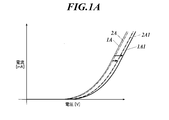
- FIG. 1A shows current-voltage characteristics 1A, 1A1 in the light-emitting region of the organic EL element of the present invention, and current-voltage characteristics 2A, 2A1 in the light-emitting area of the conventional organic EL element, and FIG.
- a conventional organic EL device having a light-emitting pattern with a predetermined shape by ultraviolet irradiation is the light-emitting pattern when the driving voltage of the device is increased by irradiating ultraviolet rays to at least one of the organic functional layers including the light-emitting layer.
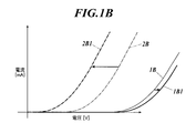
- the current-voltage characteristic 1A of the light-emitting region and the current-voltage characteristic 2B of the non-light-emitting region are approximated and are driven for a long time.
- the current-voltage characteristic 2B1 in the non-light emitting region may shift to the current-voltage characteristic 2A1 side in the light emitting region.
- the current characteristics of the non-light-emitting region are more likely to flow than in the initial stage, and the luminance of the light-emitting region is changed by changing the feeding current to the light-emitting region. It may decrease.
- any one of the organic functional layers is configured by forming an organic layer configuration in which a region where current flows when driving and a region where current is less likely to flow than the region, so that a region where current flows can be obtained.
- a light emitting region is formed, and a region where current is difficult to flow forms a non-light emitting region.
- the current-voltage characteristics 1A and 1B of both are not approximate, and even if the current-voltage characteristics 1A and 1B shift by driving for a long time,
- the current-voltage characteristic 1B1 in the light emitting region is less likely to shift to the lower voltage side than the current-voltage characteristic 1A1 in the light emitting region.
- the organic electroluminescent element of the present invention is an element having an organic functional layer including at least a hole transport layer and a light emitting layer between an anode and a cathode, and any one of the organic functional layers is a design pattern display control unit.
- the design pattern display control unit is composed of a region through which current flows when the organic electroluminescence device is driven and a region through which current is less likely to flow than the region, thereby the organic electroluminescence device. As a whole, an appropriate design pattern is displayed. This feature is a technical feature common to the inventions according to claims 1 to 5.
- control of the current amount in the region where the current flows and the region where the current hardly flows is included in the design pattern display control unit is controlled by the hole injection amount.
- the organic functional layer formed as the said design pattern display control part is at least any one layer of a positive hole injection layer and the said positive hole transport layer.
- the anode is preferably a thin film electrode mainly composed of silver.
- the display of the design pattern can be controlled by the light emission start voltage.
- the light emitting layer according to the present invention is composed of a single layer or a plurality of layers, and when there are a plurality of light emitting layers, a non-light emitting intermediate layer may be provided between the light emitting layers.
- a hole blocking layer also referred to as a hole blocking layer
- an electron injection layer also referred to as a cathode buffer layer
- An electron blocking layer also referred to as an electron barrier layer
- a hole injection layer also referred to as an anode buffer layer
- the electron transport layer according to the present invention is a layer having a function of transporting electrons, and in a broad sense, an electron injection layer and a hole blocking layer are also included in the electron transport layer and may be composed of a plurality of layers.
- the hole transport layer according to the present invention is a layer having a function of transporting holes, and in a broad sense, a hole injection layer and an electron blocking layer are also included in the hole transport layer, and are composed of a plurality of layers. Also good.
- the hole transport layer in a narrow sense may be composed of a plurality of layers.
- the layer excluding the anode and the cathode is referred to as “organic functional layer”.
- the organic EL element according to the present invention may be a so-called tandem structure element including at least one light-emitting layer and a plurality of light-emitting units composed of any one of the organic functional layers. good.
- the plurality of light emitting units may all be the same or different. Further, the two light emitting units may be the same, and the remaining one may be different.
- the plurality of light emitting units may be laminated directly or via an intermediate layer (also called an intermediate electrode, an intermediate conductive layer, a charge generation layer, an electron extraction layer, a connection layer, or an intermediate insulating layer).
- An intermediate layer also called an intermediate electrode, an intermediate conductive layer, a charge generation layer, an electron extraction layer, a connection layer, or an intermediate insulating layer.
- a known material structure can be used as long as a layer having a function of supplying electrons to the adjacent layer on the side is provided and a layer having a function of supplying holes to the adjacent layer on the cathode side is provided.
- Examples of materials used for the intermediate layer include ITO (indium tin oxide), IZO (indium zinc oxide), ZnO 2 , TiN, ZrN, HfN, TiOx, VOx, CuI, InN, GaN, and CuAlO 2. , CuGaO 2 , SrCu 2 O 2 , LaB 6 , RuO 2 , Al, etc., conductive inorganic compound layers, bilayer films and multilayer films of these conductive inorganic compounds, fullerenes such as C60, and conductivity such as oligothiophene Examples include organic material layers, conductive organic compound layers such as metal phthalocyanines, metal-free phthalocyanines, and porphyrins, but the present invention is not limited thereto.
- Preferred examples of the structure within the light emitting unit include those obtained by removing the anode and the cathode from the structures (1) to (7) mentioned in the above representative element structures, but the present invention is not limited to these. Not.
- tandem organic EL element examples include, for example, US Pat. No. 7,420,203, US Pat. No. 7,473,923, US Pat. No. 6,872,472, US Pat. No. 6,107,734, US Pat. No. 6,337,492, and JP 2011-96679A.
- the present invention is not limited to these.
- the organic EL element of the present invention includes a design pattern display control unit, and thus can emit light with a light emission pattern having a predetermined shape.
- the “design pattern” refers to a design (design or pattern in the figure), characters, images, etc. displayed by the organic EL element.
- “Patterning” or “patterning” means providing these pattern display functions.
- the “light emission pattern” of an organic EL element means that when the organic EL element emits light, the light emission intensity (luminance) is determined by the position of the light emitting surface based on a predetermined design (pattern or pattern in the figure), characters, images, etc.
- the design pattern display control unit is a layer in which any one of the organic functional layers constituting the organic EL element of the present invention is patterned using an evaporation mask, and a current flows when the organic EL element is driven. And a region where current is less likely to flow than that region.
- a region where current flows constitutes a light emitting region, and a region where current hardly flows constitutes a non-light emitting region, whereby the organic EL element of the present invention has an appropriate design pattern as the whole organic EL element.
- the region where current does not easily flow refers to a region having a current-voltage characteristic on the high voltage side of +2 V or more of the current-voltage characteristic of the region where the current flows.
- the control of the amount of current in the region where the current flows and the region where the current is less likely to flow than the region is preferably performed by controlling the hole injection amount.
- the organic EL element is formed using a hole injection layer / first hole transport layer / second hole transport layer / blue light emitting layer / green light emitting layer /
- the hole injection amount can be controlled by patterning the hole injection layer and the first hole transport layer. That is, in the region where each organic functional layer overlaps, the place where the hole injection layer and the first hole transport layer are not formed is the place where the hole injection layer and the first hole transport layer are formed.
- the amount of hole injection is smaller than that, the light emission starting voltage is increased. As a result, current easily flows in the locations where the hole injection layer and the first hole transport layer are formed, and current does not easily flow in locations where the hole injection layer and the first hole transport layer are not formed. Yes.
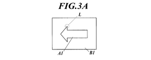
- the region where current is difficult to flow has an increased light emission start voltage as described above, but is not in a completely insulated state. Therefore, even when the light emission pattern having a predetermined shape includes a sharp shape, that is, when the region where the current easily flows in the design pattern display control unit includes a sharp shape in plan view, the organic EL element is driven. The current is not concentrated locally, and the occurrence of a short circuit can be suppressed. Specifically, for example, in a conventional organic EL element having a light emission pattern composed of a light emission region A1 and a non-light emission region B1 as shown in FIG. 3A, the non-light emission region B1 is in an electrically insulated state.
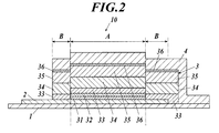
- the organic EL element 10 provided with a design pattern display control unit will be described with reference to FIG.
- the organic EL element 10 is configured by laminating an anode 2, an organic functional layer 3, a cathode 4, and the like on a substrate 1.
- the organic functional layer 3 includes a hole injection layer 31, a first hole transport layer 32, a second hole transport layer 33, a light emitting layer 34, an electron transport layer 35, and an electron injection layer 36.
- the hole injection layer 31 and the first hole transporting layer of the organic functional layer 3 are laminated.
- the hole injection layer 31 and the first hole transport layer 32 are patterned layers, and these layers constitute a design pattern display control unit.
- the amount of hole injection in the region B can be made smaller than the amount of hole injection in the region A
- the region B is a region where current does not easily flow (non-light emitting region)
- the region A is a region where current flows (light emission).
- the region B is not in a completely insulated state and a minute current flows, it is possible to suppress the current from being concentrated on the edge portion of the region A and the like, thereby suppressing the occurrence of a short circuit.
- the design pattern display control unit is configured by patterning the hole injection layer 31 and the first hole transport layer 32.
- the design pattern display control unit may be configured by patterning another organic functional layer as long as a region where current is less likely to flow can be formed.
- each light emitting unit may be provided with a design pattern display control unit, and the design pattern display control unit may be configured to emit light with different light emission patterns. good.
- the organic EL device of the present invention configured as shown in FIG. 2 has the same layer structure as that of FIG. 2, and includes a hole injection layer, a first hole transport layer, a second hole transport layer, and light emission.
- a current-voltage characteristic of a conventional organic EL element in which a light emitting pattern is provided by patterning a layer will be described with reference to FIGS. 1A and 1B.
- FIG. 1A shows current-voltage characteristics 1A, 1A1 in the light-emitting region of the organic EL element of the present invention, and current-voltage characteristics 2A, 2A1 in the light-emitting area of the conventional organic EL element
- FIG. 1B shows the organic-voltage characteristics of the present invention.
- the current-voltage characteristics 1B and 1B1 in the non-light-emitting region of the EL element and the current-voltage characteristics 2B and 2B1 in the non-light-emitting region of the conventional organic EL element are shown.
- the current-voltage characteristics 1A1, 1B1, 2A1, and 2B1 indicate the current-voltage characteristics after each organic EL element is driven for a long time.
- the conventional organic EL element can emit light with the light emission pattern by forming a light emitting layer or the like in the organic functional layer in a predetermined pattern shape.
- the current-voltage characteristic 2A in the light-emitting region and the current-voltage characteristic 2B in the non-light-emitting region are approximated, and the current voltage in the non-light-emitting region is obtained by being driven for a long time.
- the characteristic 2B1 may shift to a lower voltage side than the current-voltage characteristic 2A1 of the light emitting region. For this reason, in the conventional organic EL element after long-time driving, current flows more easily in the non-light-emitting region than in the light-emitting region, and the current supplied to the light-emitting region is reduced, thereby reducing the light-emitting region. In some cases, the brightness of the image may decrease.
- the hole injection layer and the first hole transport layer in the organic functional layer constitute a design pattern display control unit, and the design pattern display control unit flows a current during driving. Since the region and the region where current is less likely to flow than the region are configured, the region where current flows is a light emitting region, and the region where current is difficult to flow is a non-light emitting region.
- the current-voltage characteristics 1A and 1B of both are not approximate, and even if the current-voltage characteristics 1A and 1B shift by driving for a long time,
- the current-voltage characteristic 1B1 in the light emitting region is less likely to shift to the lower voltage side than the current-voltage characteristic 1A1 in the light emitting region.
- the layer thickness of the hole injection layer is preferably 2 to 50 nm, and more preferably 2 to 30 nm. .
- the hole transport layer is provided adjacent to the hole injection layer.
- the layer thickness of the hole transport layer is less than 15 nm, the durability of the organic EL element is lowered.
- the thickness of the hole transport layer exceeds 200 nm, the color difference when the viewing angle is changed becomes large, and the amount of light generated in the light emitting layer is increased. It may be blurred. Therefore, when the design pattern display control unit is configured by patterning the hole injection layer and the hole transport layer, the layer thickness of the hole transport layer is preferably 15 to 200 nm, preferably 20 to 150 nm. More preferably.
- the light emitting layer preferably contains a host compound and a light emitting dopant.
- the light emitting dopant contained in the light emitting layer may be contained at a uniform concentration or may have a concentration distribution in the thickness direction of the light emitting layer.
- the thickness of each light emitting layer included in each light emitting unit is not particularly limited, but the homogeneity of a layer to be formed and a high voltage unnecessary for light emission are not required. From the viewpoint of preventing the application and improving the stability of the luminescent color with respect to the drive current, it is preferably adjusted in the range of 5 to 200 nm, more preferably in the range of 10 to 100 nm.
- the phosphorescent host compound and phosphorescent dopant contained in the light emitting layer will be described.
- Phosphorescent host compound used in the present invention is not particularly limited in terms of structure, but typically includes, for example, a carbazole derivative, a triarylamine derivative, an aromatic borane derivative, Those having basic skeletons such as nitrogen heterocyclic compounds, thiophene derivatives, furan derivatives, oligoarylene compounds, carboline derivatives and diazacarbazole derivatives (here, diazacarbazole derivatives are carbonizations constituting the carboline ring of carboline derivatives) And the like in which at least one carbon atom of the hydrogen ring is substituted with a nitrogen atom.
- the phosphorescent host compound may be used alone or in combination of two or more.
- the phosphorescent host compound used in the light emitting layer according to the present invention is preferably a compound represented by the following general formula (a).
- X represents NR ′, O, S, CR′R ′′ or SiR′R ′′.
- R ′ and R ′′ each independently represents a hydrogen atom or a substituent.
- Ar represents an aromatic ring.
- N represents an integer of 0 to 8.
- examples of the substituent represented by R ′ and R ′′ include an alkyl group (for example, a methyl group, an ethyl group, a propyl group, an isopropyl group, a tert-butyl group, a pentyl group, a hexyl group).
- an alkyl group for example, a methyl group, an ethyl group, a propyl group, an isopropyl group, a tert-butyl group, a pentyl group, a hexyl group.
- X preferably represents NR ′ or O
- R ′ particularly preferably represents an aromatic hydrocarbon group or an aromatic heterocyclic group.
- examples of the aromatic ring represented by Ar include an aromatic hydrocarbon ring and an aromatic heterocyclic ring.
- the aromatic ring represented by Ar may be either a single ring or a condensed ring, and further has a substituent represented by the above-mentioned R ′ and R ′′ even if it is unsubstituted. May be.
- examples of the aromatic hydrocarbon ring represented by Ar include a benzene ring, biphenyl ring, naphthalene ring, azulene ring, anthracene ring, phenanthrene ring, pyrene ring, chrysene ring, naphthacene ring, and triphenylene.
- examples of the aromatic heterocycle represented by Ar include a furan ring, a dibenzofuran ring, a thiophene ring, an oxazole ring, a pyrrole ring, a pyridine ring, a pyridazine ring, a pyrimidine ring, a pyrazine ring, and a triazine ring.
- the aromatic ring represented by Ar is preferably a carbazole ring, carboline ring, dibenzofuran ring or benzene ring, more preferably a carbazole ring, carboline ring or benzene ring, Preferred is a benzene ring having a substituent, and most preferred is a benzene ring having a carbazolyl group.
- the aromatic ring represented by Ar is preferably a condensed ring having three or more rings, as shown below.
- Specific examples of the aromatic hydrocarbon condensed ring in which three or more rings are condensed include, for example, naphthacene ring, anthracene ring, tetracene ring, pentacene ring, hexacene ring, phenanthrene ring, pyrene ring, benzopyrene ring, benzoazulene ring, Chrysene ring, benzochrysene ring, acenaphthene ring, acenaphthylene ring, triphenylene ring, coronene ring, benzocoronene ring, hexabenzocoronene ring, fluorene ring, benzofluorene ring, fluoranthene ring, perylene ring, naphthoperylene ring, penta
- n represents an integer of 0 to 8, preferably an integer of 0 to 2, particularly 1 or 2 when X is O or S. It is preferable.
- the phosphorescent host compound used in the present invention may be a low molecular compound or a high molecular compound having a repeating unit, and a low molecular compound having a polymerizable group such as a vinyl group or an epoxy group (evaporation polymerizable light emitting host). But it ’s okay.
- the phosphorescent host compound a compound having a hole transporting ability and an electron transporting ability, which prevents emission of light from being increased in wavelength and has a high Tg (glass transition temperature) is preferable.
- a compound having a glass transition point of 90 ° C. or higher is preferable, and a compound having a glass transition temperature of 130 ° C. or higher is preferable because excellent characteristics can be obtained.
- the glass transition point (Tg) is a value obtained by a method based on JIS K 7121 using DSC (Differential Scanning Calorimetry).
- a conventionally known host compound can also be used.
- conventionally known host compounds compounds described in the following documents can be suitably used.
- the phosphorescent host compound may be different for each light emitting layer of each light emitting unit, but the same compound is preferable in terms of production efficiency and process management.
- the phosphorescent host compound preferably has a lowest excited triplet energy (T1) larger than 2.7 eV because higher luminous efficiency can be obtained.
- the lowest excited triplet energy as used in the present invention refers to the peak energy of an emission band corresponding to the transition between the lowest vibrational bands of a phosphorescence emission spectrum observed at a liquid nitrogen temperature after dissolving a host compound in a solvent.
- the phosphorescence emission dopant which can be used for this invention can be selected from a well-known thing. For example, it can be selected from complex compounds containing metals of Group 8 to Group 10 in the periodic table of elements, preferably iridium compounds, osmium compounds or platinum compounds (platinum complex compounds), or rare earth complexes. Of these, iridium compounds are most preferred.
- a phosphorescent light emitting material is preferable as a light emitter that emits light in at least the green, yellow, and red regions.
- Ra represents a hydrogen atom, an aliphatic group, an aromatic group or a heterocyclic group.
- Rb and Rc each independently represents a hydrogen atom or a substituent.
- A1 represents a residue necessary for forming an aromatic ring or an aromatic heterocyclic ring.
- M represents Ir or Pt.
- Ra represents a hydrogen atom, an aliphatic group, an aromatic group, or a heterocyclic group.
- Rb, Rc, Rb 1 and Rc 1 each independently represent a hydrogen atom or a substituent.
- A1 represents a residue necessary for forming an aromatic ring or an aromatic heterocyclic ring.
- M represents Ir or Pt.
- Ra represents a hydrogen atom, an aliphatic group, an aromatic group or a heterocyclic group.
- Rb and Rc each independently represents a hydrogen atom or a substituent.
- A1 represents a residue necessary for forming an aromatic ring or an aromatic heterocyclic ring.
- M represents Ir or Pt.
- examples of the aliphatic group represented by Ra include an alkyl group (eg, methyl group, ethyl group, propyl group, butyl group, pentyl group, isopentyl group, 2-ethyl group). -Hexyl group, octyl group, undecyl group, dodecyl group, tetradecyl group) and cycloalkyl group (for example, cyclopentyl group, cyclohexyl group).
- alkyl group eg, methyl group, ethyl group, propyl group, butyl group, pentyl group, isopentyl group, 2-ethyl group.
- cycloalkyl group for example, cyclopentyl group, cyclohexyl group.
- Examples of the aromatic group represented by Ra include a phenyl group, a tolyl group, an azulenyl group, an anthranyl group, a phenanthryl group, a pyrenyl group, a chrycenyl group, a naphthacenyl group, an o-terphenyl group, an m-terphenyl group, p -Terphenyl group, acenaphthenyl group, coronenyl group, fluorenyl group, perylenyl group and the like.
- heterocyclic group represented by Ra examples include pyrrolyl, indolyl, furyl, thienyl, imidazolyl, pyrazolyl, indolizinyl, quinolinyl, carbazolyl, indolinyl, thiazolyl, pyridyl, pyridazinyl.
- These groups may have a substituent represented by R ′ and R ′′ in the general formula (a).
- examples of the substituent represented by Rb, Rc, Rb 1 and Rc 1 include an alkyl group (eg, methyl group, ethyl group, propyl group, isopropyl group, tert- Butyl group, pentyl group, hexyl group, octyl group, dodecyl group, tridecyl group, tetradecyl group, pentadecyl group, etc.), cycloalkyl group (eg, cyclopentyl group, cyclohexyl group, etc.), alkenyl group (eg, vinyl group, allyl group) Etc.), alkynyl groups (eg ethynyl group, propargyl group etc.), aryl groups (eg phenyl group, naphthyl group etc.), aromatic heterocyclic groups (eg furyl group, thienyl group, pyridyl
- examples of the aromatic ring represented by A1 include a benzene ring, biphenyl ring, naphthalene ring, azulene ring, anthracene ring, phenanthrene ring, pyrene ring, chrysene ring, and naphthacene ring.
- Triphenylene ring Triphenylene ring, o-terphenyl ring, m-terphenyl ring, p-terphenyl ring, acenaphthene ring, coronene ring, fluorene ring, fluoranthrene ring, naphthacene ring, pentacene ring, perylene ring, pentaphen ring, picene ring , Pyrene ring, pyranthrene ring, anthraanthrene ring and the like.
- aromatic heterocycle represented by A1 for example, furan ring, thiophene ring, pyridine ring, pyridazine ring, pyrimidine ring, pyrazine ring, triazine ring, benzimidazole ring, oxadiazole ring, triazole ring, imidazole ring, Pyrazole ring, thiazole ring, indole ring, benzimidazole ring, benzothiazole ring, benzoxazole ring, quinoxaline ring, quinazoline ring, phthalazine ring, carbazole ring, carboline ring, diazacarbazole ring (the hydrocarbon ring constituting the carboline ring) A ring in which one of the carbon atoms is substituted with a nitrogen atom.) And the like.
- M represents Ir or Pt, with Ir being preferred.
- the structures of the general formulas (A) to (C) are partial structures, and a ligand corresponding to the valence of the central metal is necessary for the structure itself to be a light-emitting dopant of a completed structure.
- ligands include, for example, halogen (eg, fluorine atom, chlorine atom, bromine atom or iodine atom), aryl group (eg, phenyl group, p-chlorophenyl group, mesityl group, Tolyl group, xylyl group, biphenyl group, naphthyl group, anthryl group, phenanthryl group, etc.), alkyl group (for example, methyl group, ethyl group, isopropyl group, hydroxyethyl group, methoxymethyl group, trifluoromethyl group, t-butyl) Group), alkyloxy group, aryloxy group, alkylthio group, arylthio group,
- a tris body having a completed structure with three partial structures of the general formulas (A) to (C) is preferable.
- Fluorescent luminescent dopants include coumarin dyes, pyran dyes, cyanine dyes, croconium dyes, squalium dyes, oxobenzanthracene dyes. Fluorescein dyes, rhodamine dyes, pyrylium dyes, perylene dyes, stilbene dyes, polythiophene dyes, rare earth complex phosphors, and the like.
- Injection layer hole injection layer, electron injection layer
- the injection layer can be provided as necessary, and exists between the anode or the intermediate layer and the light emitting layer or the hole transport layer, or between the cathode or the intermediate layer and the light emitting layer or the electron transport layer. Also good.
- the injection layer is a layer provided between the electrode and the intermediate layer and the organic layer in order to lower the driving voltage and improve the light emission luminance.
- the injection layer is a layer provided between the electrode and the intermediate layer and the organic layer in order to lower the driving voltage and improve the light emission luminance.
- the organic EL element and its forefront of industrialization June 30, 1998 The details are described in Chapter 2, “Electrode Materials” (pages 123 to 166) of Volume 2 of “T.S. Co., Ltd.”.
- the hole injection layer (anode buffer layer) and the electron injection layer (cathode buffer) Layer The hole injection layer (anode buffer layer) and the electron injection layer (cathode buffer) Layer).
- hole injection layer anode buffer layer
- JP-A-9-45479 JP-A-9-260062, JP-A-8-288069, and the like.
- Specific examples thereof include copper phthalocyanine.
- Phthalocyanine buffer layer typified by (1), oxide buffer layer typified by vanadium oxide, amorphous carbon buffer layer, polymer buffer layer using a conductive polymer such as polyaniline (emeraldine) or polythiophene, and the like. It is also preferable to use the materials described in JP-T-2003-519432.
- the hole injection layer may be used by mixing a plurality of materials, but in the present invention, the hole injection layer is preferably formed by forming a single organic compound.
- the reason for this is that when a plurality of materials are mixed and used, the risk of performance fluctuations due to fluctuations in the mixing ratio during production, for example, concentration fluctuations in the film formation substrate surface, is increased.
- the layer thickness of the hole injection layer is not particularly limited, and is usually in the range of about 0.1 to 100 nm. However, in the present invention, it is preferably in the range of 2 to 50 nm. More preferably within the range.
- Suitable materials for the electron injection layer include alkali metals, alkaline earth metals, and compounds thereof having a work function of 3 eV or less in the electron injection layer provided between the electron transport layer and the cathode.
- Specific examples of the alkali metal compound include potassium fluoride, lithium fluoride, sodium fluoride, cesium fluoride, lithium oxide, lithium quinoline complex, cesium carbonate and the like, and lithium fluoride and cesium fluoride are preferable.
- As a layer adjacent to the anode side of the intermediate layer it is preferable not to provide a layer made of an alkali metal compound or an alkaline earth compound.
- the layer thickness of the electron injection layer is not particularly limited, but is usually in the range of about 0.1 to 10 nm, preferably in the range of 0.1 to 2 nm.
- ⁇ Blocking layer hole blocking layer, electron blocking layer>
- the blocking layer is provided as necessary. For example, it is described in JP-A Nos. 11-204258 and 11-204359, and “Organic EL elements and the forefront of industrialization (published by NTT Corporation on November 30, 1998)” on page 237. There is a hole blocking (hole blocking) layer.
- the hole blocking layer has a function of an electron transport layer in a broad sense, and is made of a hole blocking material having a function of transporting electrons and a very small ability to transport holes. By blocking the holes, the probability of recombination of electrons and holes can be improved. Moreover, the structure of the electron carrying layer mentioned later can be used as a hole-blocking layer as needed.
- the hole blocking layer is preferably provided adjacent to the light emitting layer.
- the electron blocking layer has a function of a hole transport layer in a broad sense, and is made of a material having a function of transporting holes while having a remarkably small ability to transport electrons. The probability of recombination of electrons and holes can be improved by blocking. Moreover, the structure of the positive hole transport layer mentioned later can be used as an electron blocking layer as needed.
- the layer thickness of the hole blocking layer and the electron blocking layer according to the present invention is preferably in the range of 3 to 100 nm, and more preferably in the range of 5 to 30 nm.
- the hole transport layer is made of a hole transport material having a function of transporting holes, and in a broad sense, a hole injection layer and an electron blocking layer are also included in the hole transport layer.
- the hole transport layer can be provided as a single layer or a plurality of layers.
- the hole transport material has either hole injection or transport or electron barrier properties, and may be either organic or inorganic.
- triazole derivatives oxadiazole derivatives, imidazole derivatives, polyarylalkane derivatives, pyrazoline derivatives and pyrazolone derivatives, phenylenediamine derivatives, arylamine derivatives, amino-substituted chalcone derivatives, oxazole derivatives, styrylanthracene derivatives, fluorenone derivatives, hydrazone derivatives
- Examples thereof include stilbene derivatives, silazane derivatives, aniline copolymers, conductive polymer oligomers, particularly thiophene oligomers.
- hole transporting material those described above can be used, but it is further preferable to use a porphyrin compound, an aromatic tertiary amine compound, and a styrylamine compound, particularly an aromatic tertiary amine compound.
- aromatic tertiary amine compounds and styrylamine compounds include N, N, N ′, N′-tetraphenyl-4,4′-diaminophenyl, N, N′-diphenyl-N, N′— Bis (3-methylphenyl)-[1,1'-biphenyl] -4,4'-diamine (TPD), 2,2-bis (4-di-p-tolylaminophenyl) propane, 1,1-bis (4-di-p-tolylaminophenyl) cyclohexane, N, N, N ′, N′-tetra-p-tolyl-4,4′-diaminobiphenyl, 1,1-bis (4-di-p-tolyl) Aminophenyl) -4-phenylcyclohexane, bis (4-dimethylamino-2-methylphenyl) phenylmethane, bis (4-di-p-tolylaminoph
- a polymer material in which these materials are introduced into a polymer chain or these materials are used as a polymer main chain can also be used.
- inorganic compounds such as p-type-Si and p-type-SiC can also be used as the hole injection material and the hole transport material.
- the hole transport layer may have a single layer structure composed of one or more of the above materials.
- the layer thickness of the hole transport layer is not particularly limited and is usually in the range of about 5 nm to 5 ⁇ m. In the present invention, it is preferably in the range of 15 to 200 nm, and in the range of 20 to 150 nm. It is more preferable that
- the electron transport layer is made of a material having a function of transporting electrons.
- the electron transport layer can be provided as a single layer or a plurality of layers.
- the electron transport material used for the electron transport layer may be any material selected from conventionally known compounds as long as it has a function of transmitting electrons injected through the cathode or intermediate layer to the light emitting layer.
- a thiadiazole derivative in which the oxygen atom of the oxadiazole ring is substituted with a sulfur atom, and a quinoxaline derivative having a quinoxaline ring known as an electron-withdrawing group can also be used as an electron transport material.
- a polymer material in which these materials are introduced into a polymer chain or these materials are used as a polymer main chain can also be used.
- a compound including a pyridine ring in the structure is preferable.
- metal complexes of 8-quinolinol derivatives such as tris (8-quinolinol) aluminum (Alq), tris (5,7-dichloro-8-quinolinol) aluminum, tris (5,7-dibromo-8-quinolinol) aluminum Tris (2-methyl-8-quinolinol) aluminum, tris (5-methyl-8-quinolinol) aluminum, bis (8-quinolinol) zinc (Znq), and the like, and the central metals of these metal complexes are In, Mg, Metal complexes replaced with Cu, Ca, Sn, Ga, or Pb can also be used as the electron transport material.
- metal-free or metal phthalocyanine or those having terminal ends substituted with an alkyl group or a sulfo group can be preferably used as the electron transporting material.
- distyrylpyrazine derivatives that are also used as a material for the light emitting layer can be used as an electron transport material.
- n-type-Si, n-type-SiC, etc. Inorganic semiconductors can also be used as electron transport materials.
- a plurality of materials may be mixed and used for the electron transport layer.
- Alkali metal, alkaline earth metal, alkali metal compound or alkaline earth metal compound can be doped, but the electron transport layer according to the present invention is formed by forming a single organic compound. Is preferred. The reason for this is that when a plurality of materials are mixed and used, the risk of performance fluctuations due to fluctuations in the mixing ratio during production, for example, concentration fluctuations in the film formation substrate surface, is increased.
- an intermediate layer having a low work function a suitable performance can be obtained without impairing the electron injection property from the intermediate layer without doping with an alkali metal or the like.
- the glass transition temperature of the organic compound contained in the electron transport layer is 110 ° C. or higher because better high temperature storage stability and high temperature process stability can be obtained.
- the layer thickness of the electron transport layer is not particularly limited, but is usually in the range of about 5 nm to 5 ⁇ m, preferably in the range of 5 to 200 nm.
- the support substrate (also referred to as a base, substrate, base material, or support) applied to the organic EL device of the present invention is not particularly limited in the type of glass, plastic, etc., and is transparent or opaque. There may be.
- the support substrate is preferably transparent. Examples of the transparent support substrate preferably used include glass, quartz, and a transparent resin film.
- a particularly preferable support substrate is a resin film capable of giving flexibility to the organic EL element.
- polyesters such as polyethylene terephthalate (PET) and polyethylene naphthalate (PEN), polyethylene, polypropylene, cellophane, cellulose diacetate, cellulose triacetate (TAC), cellulose acetate butyrate, cellulose acetate propionate ( CAP), cellulose esters such as cellulose acetate phthalate, cellulose nitrate or derivatives thereof, polyvinylidene chloride, polyvinyl alcohol, polyethylene vinyl alcohol, syndiotactic polystyrene, polycarbonate, norbornene resin, polymethylpentene, polyether ketone, polyimide , Polyethersulfone (PES), polyphenylene sulfide, polysulfones Cycloolefins such as polyetherimide, polyetherketoneimide, polyamide, fluororesin, nylon, polymethylmethacrylate, acrylic or polyarylate, arton (trade name, manufactured by JSR) or abortion (trade name,
- An inorganic or organic film or a hybrid film of both may be formed on the surface of the resin film, and the water vapor permeability measured by a method in accordance with JIS K 7129-1992 is 0.01 g / (m 2 24h)
- the following gas barrier film is preferable, and the oxygen permeability measured by a method according to JIS K 7126-1992 is 1 ⁇ 10 ⁇ 3 ml / (m 2 ⁇ 24h ⁇ atm).
- a high gas barrier film having a water vapor permeability of 1 ⁇ 10 ⁇ 3 g / (m 2 ⁇ 24 h) or less is preferable, and further, an oxygen permeability is 1 ⁇ 10 ⁇ 5 ml / (m 2 It is particularly preferable that the water vapor permeability is 1 ⁇ 10 ⁇ 5 g / (m 2 ⁇ 24 h) or less.
- any material may be used as long as it has a function of suppressing intrusion of elements that cause deterioration of elements such as moisture and oxygen.
- silicon oxide, silicon dioxide, silicon nitride, or the like can be used.
- the method for forming the gas barrier film is not particularly limited.
- a plasma CVD method, a laser CVD method, a thermal CVD method, a coating method, and the like can be used, but those using an atmospheric pressure plasma polymerization method as described in JP-A-2004-68143 are also preferably used. be able to.
- the opaque support substrate examples include metal plates / films such as aluminum and stainless steel, opaque resin substrates, ceramic substrates, and the like.
- sealing means used for sealing the organic EL element of the present invention include a method of bonding a sealing member, an electrode, and a support substrate with an adhesive.
- the sealing member may be disposed so as to cover the display area of the organic EL element, and may be concave or flat. Moreover, transparency and electrical insulation are not particularly limited.
- Specific examples include a glass plate, a polymer plate / film, and a metal plate / film.
- the glass plate include soda-lime glass, barium / strontium-containing glass, lead glass, aluminosilicate glass, borosilicate glass, barium borosilicate glass, and quartz.
- the polymer plate include polycarbonate, acrylic, polyethylene terephthalate, polyether sulfide, and polysulfone.
- the metal plate include those made of one or more metals or alloys selected from the group consisting of stainless steel, iron, copper, aluminum, magnesium, nickel, zinc, chromium, titanium, molybdenum, silicon, germanium, and tantalum.
- a polymer film or a metal film can be preferably used because the organic EL element can be thinned.
- the polymer film has an oxygen permeability of 1 ⁇ 10 ⁇ 3 ml / (m 2 ⁇ 24 h ⁇ atm) or less and a water vapor permeability of 1 ⁇ 10 ⁇ 3 g / (m 2 ⁇ 24 h) or less.
- the oxygen permeability is 1 ⁇ 10 ⁇ 5 ml / (m 2 ⁇ 24 h ⁇ atm) or less
- the water vapor permeability is 1 ⁇ 10 ⁇ 5 g / (m 2 ⁇ 24 h).
- sealing member For processing the sealing member into a concave shape, sandblasting, chemical etching, or the like is used.
- the adhesive include photocuring and thermosetting adhesives having reactive vinyl groups of acrylic acid oligomers and methacrylic acid oligomers, and moisture curing adhesives such as 2-cyanoacrylates. Can be mentioned. Moreover, heat
- an organic EL element may deteriorate by heat processing, what can be adhesive-hardened from room temperature (25 degreeC) to 80 degreeC is preferable.
- a desiccant may be dispersed in the adhesive.
- coating of the adhesive agent to a sealing part may use commercially available dispenser, and may print like screen printing.
- an inert gas such as nitrogen or argon, or an inert liquid such as fluorinated hydrocarbon or silicon oil is injected in the gas phase and the liquid phase.
- a vacuum can also be used.
- a hygroscopic compound can also be enclosed inside.
- hygroscopic compound examples include metal oxides (for example, sodium oxide, potassium oxide, calcium oxide, barium oxide, magnesium oxide, aluminum oxide) and sulfates (for example, sodium sulfate, calcium sulfate, magnesium sulfate, cobalt sulfate).
- metal oxides for example, sodium oxide, potassium oxide, calcium oxide, barium oxide, magnesium oxide, aluminum oxide
- sulfates for example, sodium sulfate, calcium sulfate, magnesium sulfate, cobalt sulfate.
- metal halides eg calcium chloride, magnesium chloride, cesium fluoride, tantalum fluoride, cerium bromide, magnesium bromide, barium iodide, magnesium iodide etc.
- perchloric acids eg perchloric acid Barium, magnesium perchlorate, and the like
- anhydrous salts are preferably used in sulfates, metal halides, and perchloric acids.
- a protective film or a protective plate may be provided outside the sealing film.
- the mechanical strength is not necessarily high, and thus it is preferable to provide such a protective film and a protective plate.
- the same glass plate, polymer plate / film, metal plate / film, etc., used for the above-mentioned sealing can be used. It is preferable to use a film.
- an electrode material made of a metal, an alloy, an electrically conductive compound or a mixture thereof having a high work function (4 eV or more) is preferably used.
- electrode materials include metals such as Au, Ag, and Al, and conductive transparent materials such as CuI, indium tin oxide (ITO), SnO 2 , and ZnO.
- conductive transparent materials such as CuI, indium tin oxide (ITO), SnO 2 , and ZnO.
- an amorphous material such as IDIXO (In 2 O 3 —ZnO) that can form a transparent conductive film may be used.
- a thin film may be formed by depositing these electrode materials by a method such as vapor deposition or sputtering, and a pattern having a desired shape may be formed by a photolithography method, or when the pattern accuracy is not required (100 ⁇ m or more) Degree), a pattern may be formed through a mask having a desired shape when the electrode material is deposited or sputtered.
- wet film-forming methods such as a printing system and a coating system, can also be used.
- the transmittance is preferably greater than 10%.
- the sheet resistance value as the anode is preferably several hundred ⁇ / ⁇ or less.
- the film thickness depends on the material, it is usually selected within the range of 5 to 1000 nm, preferably within the range of 5 to 200 nm.
- the anode is preferably a thin film electrode mainly composed of silver.
- the anode preferably has a two-layer structure in which a base layer and an electrode layer are sequentially laminated from the substrate side, for example.
- the electrode layer is a layer composed of silver or an alloy containing silver as a main component
- the underlayer is a layer composed of, for example, a compound containing nitrogen atoms.
- a main component means that content in an electrode layer is 50 mass% or more.
- the underlayer is a layer provided on the substrate side of the electrode layer.
- the material constituting the underlayer is not particularly limited as long as it can suppress aggregation of silver when forming an electrode layer made of silver or an alloy containing silver as a main component.
- nitrogen Examples thereof include nitrogen-containing compounds containing atoms.
- the upper limit of the layer thickness needs to be less than 50 nm, preferably less than 30 nm, and preferably less than 10 nm. More preferably, it is particularly preferably less than 5 nm.
- the lower limit of the layer thickness is required to be 0.05 nm or more, preferably 0.1 nm or more, and particularly preferably 0.3 nm or more.
- the upper limit of the layer thickness is not particularly limited, and the lower limit of the layer thickness is the same as that of the low refractive index material. .
- the layer is formed with a necessary layer thickness that allows uniform film formation.
- a method for forming the underlayer for example, a method using a wet process such as a coating method, an ink jet method, a coating method, a dip method, a dry method such as a vapor deposition method (resistance heating, EB method, etc.), a sputtering method, a CVD method, etc. Examples include a method using a process. Among these, the vapor deposition method is preferably applied.
- the compound containing a nitrogen atom constituting the underlayer is not particularly limited as long as it is a compound containing a nitrogen atom in the molecule, but is preferably a compound having a heterocycle having a nitrogen atom as a heteroatom.
- the heterocycle having a nitrogen atom as a hetero atom include, for example, aziridine, azirine, azetidine, azeto, azolidine, azole, azinane, pyridine, azepan, azepine, imidazole, pyrazole, oxazole, thiazole, imidazoline, pyrazine, morpholine, thiazine, Indole, isoindole, benzimidazole, purine, quinoline, isoquinoline, quinoxaline, cinnoline, pteridine, acridine, carbazole, benzo-C-cinnoline, porphyrin, chlorin, choline and
- Electrode layer As a method for forming the electrode layer, for example, a method using a wet process such as a coating method, an inkjet method, a coating method, a dip method, a vapor deposition method (resistance heating, EB method, etc.), a sputtering method, Examples include a method using a dry process such as a CVD method. Among these, the vapor deposition method is preferably applied.
- the electrode layer is formed on the underlayer so that it is sufficiently conductive without high-temperature annealing after the electrode layer is formed. It may be subjected to a high temperature annealing treatment or the like later.
- Examples of the alloy mainly composed of silver (Ag) constituting the electrode layer include silver magnesium (AgMg), silver copper (AgCu), silver palladium (AgPd), silver palladium copper (AgPdCu), and silver indium (AgIn). Etc.
- the electrode layer as described above may have a structure in which silver or an alloy layer mainly composed of silver is divided into a plurality of layers as necessary.
- the electrode layer preferably has a layer thickness in the range of 4 to 9 nm.
- the layer thickness is less than 9 nm, the absorption component or reflection component of the layer is small, and the transmittance of the anode is increased. Further, when the layer thickness is thicker than 4 nm, the conductivity of the layer can be sufficiently secured.
- the anode of the laminated structure composed of the base layer as described above and the electrode layer formed thereon is covered with a protective film on the upper part of the electrode layer or another electrode layer is laminated. May be.
- the protective film and the other electrode layer have optical transparency so as not to impair the optical transparency of the anode.
- cathode On the other hand, as a cathode, what uses a metal, an alloy, an electroconductive compound, and these mixtures as an electrode substance is used. Specific examples of such electrode materials include sodium, sodium-potassium alloy, magnesium, lithium, magnesium / copper mixture, magnesium / silver mixture, magnesium / aluminum mixture, magnesium / indium mixture, aluminum / aluminum oxide (Al 2 O 3 ) Mixtures, indium, lithium / aluminum mixtures, rare earth metals, silver, aluminum and the like.
- a mixture of an electron injecting metal and a second metal which is a stable metal having a larger work function value than this for example, a magnesium / silver mixture, magnesium / Aluminum mixture, magnesium / indium mixture, aluminum / aluminum oxide (Al 2 O 3 ) mixture, lithium / aluminum mixture, aluminum, silver and the like are suitable.
- the cathode can be produced by forming a thin film of these electrode materials by a method such as vapor deposition or sputtering.
- the sheet resistance value as the cathode is preferably several hundred ⁇ / ⁇ or less, and the film thickness is usually selected within the range of 5 nm to 5 ⁇ m, preferably within the range of 5 to 200 nm.
- a transparent or semi-transparent cathode can be produced by producing the conductive transparent material mentioned in the description of the anode on the cathode after producing the above material with a film thickness in the range of 1 to 20 nm. By applying this, an element in which both the anode and the cathode are transmissive can be manufactured.
- the following polysilazane-containing liquid was applied with a wireless bar so that the average film thickness after drying was 300 nm, and was dried by heat treatment for 1 minute in an atmosphere of temperature 85 ° C. and humidity 55% RH. Subsequently, it was kept in an atmosphere of a temperature of 25 ° C. and a humidity of 10% RH (dew point temperature ⁇ 8 ° C.) for 10 minutes to perform dehumidification treatment, thereby forming a polysilazane-containing layer on the transparent substrate.
- polysilazane-containing liquid a 10% by mass dibutyl ether solution of perhydropolysilazane (Aquamica NN120-10, non-catalytic type, manufactured by AZ Electronic Materials Co., Ltd.) was used.
- the transparent substrate on which the polysilazane-containing layer is formed is fixed on the operation stage of an excimer irradiation apparatus MECL-M-1-200 (manufactured by M.D. Com) and reformed under the following reforming conditions.
- the polysilazane modified layer having a layer thickness of 300 nm was formed.
- Irradiation wavelength 172 nm
- Lamp filled gas Xe Excimer lamp light intensity: 130 mW / cm 2 (172 nm)
- Distance between sample and light source 1mm
- silver was vapor-deposited with a thickness of 10 nm on the underlayer by a vapor deposition method to form an anode.
- the transparent substrate on which the anode was formed was ultrasonically cleaned with isopropyl alcohol, dried with dry nitrogen gas, and subjected to UV ozone cleaning for 5 minutes, and then the transparent substrate was fixed to a substrate holder of a commercially available vacuum deposition apparatus.
- Each of the vapor deposition crucibles in the vacuum vapor deposition apparatus was filled with the constituent material of each layer in an amount optimal for device fabrication.
- the evaporation crucible used was made of a resistance heating material made of molybdenum or tungsten.
- first hole transport layer (Formation of first hole transport layer) Next, Compound M-2 was deposited at a deposition rate of 0.1 nm / second to form a first hole transport layer having a layer thickness of 40 nm. In the formation of the first hole transport layer, vapor deposition was performed using a metal mask for vapor deposition capable of patterning the shape shown in FIG. 3A in the same manner as the hole injection layer.
- Compound E-1 was deposited at a deposition rate of 0.1 nm / second to form an electron transport layer having a layer thickness of 30 nm.
- the transparent sealing substrate is bonded using an epoxy thermosetting adhesive (Elephan CS manufactured by Yodogawa Paper Co., Ltd.) as an adhesive, in a glove box having an oxygen concentration of 10 ppm or less and a water concentration of 10 ppm or less, at 80 ° C. and 0. Under a load of 04 MPa, pressure reduction (1 ⁇ 10 ⁇ 3 MPa or less) is applied for 20 seconds, and pressing is performed for 20 seconds. It was vacuum-pressed to become.
- an epoxy thermosetting adhesive Elephan CS manufactured by Yodogawa Paper Co., Ltd.
- the adhesive layer was thermally cured by heating on a hot plate at 110 ° C. for 30 minutes.
- an organic EL element 101 having a light emission pattern composed of a light emitting region A1 and a non-light emitting region B1 as shown in FIG. 3A was obtained.
- Formation of intermediate layer Aluminum was vapor-deposited on the electron injection layer by a vapor deposition method to provide an intermediate layer having a layer thickness of 10 nm.
- Compound M-4 was deposited at a deposition rate of 0.1 nm / second to provide a hole injection layer having a layer thickness of 15 nm.
- vapor deposition was performed using a metal mask for vapor deposition that can pattern the shape shown in FIG. 3B.
- Compound M-2 was deposited at a deposition rate of 0.1 nm / second to provide a first hole transport layer having a layer thickness of 50 nm.
- it vapor-deposited using the metal mask for vapor deposition which can pattern the shape shown to FIG. 3B similarly to a positive hole injection layer.
- the compound NPD was deposited at a deposition rate of 0.1 nm / second to provide a second hole transport layer having a layer thickness of 50 nm.
- Compound E-1 was deposited at a deposition rate of 0.1 nm / second to form an electron transport layer having a layer thickness of 30 nm.
- the organic EL element 101 of the present invention has a lower luminance change rate than the organic EL element 104 of the comparative example.
- the organic EL element 101 of the present invention has a light emission pattern of a predetermined shape and can suppress a decrease in light emission luminance of the light emitting region even when driven for a long time.
- the same effect is obtained for the organic EL element 102 having a tandem structure.
- the luminance reduction rate of the organic EL elements 101 and 102 of the present invention is approximately the same as that of the organic EL element 103 that is not patterned, and can exhibit the same performance as the organic EL element that does not have a light emission pattern. It can be said.
- the present invention is suitable for providing an organic electroluminescence device having a light emission pattern of a predetermined shape and capable of suppressing a decrease in light emission luminance of a light emitting region even when driven for a long time.
Landscapes
- Physics & Mathematics (AREA)
- Optics & Photonics (AREA)
- Electroluminescent Light Sources (AREA)
Abstract
La présente invention concerne un élément électroluminescent organique présentant un motif d'émission lumineuse d'une forme prédéterminée et apte à supprimer les réductions de la luminosité de la lumière émise par les régions d'émission lumineuse, même après une longue période de fonctionnement. Ledit élément électroluminescent organique (10) est caractérisé en ce qu'il présente dans l'ensemble un modèle de conception approprié du fait qu'il comprend des couches fonctionnelles organiques (3) qui comprennent au moins des couches de transport de trous (32, 33) et une couche d'émission lumineuse (34) entre une électrode positive (2) et une électrode négative (4). Ledit élément électroluminescent organique (10) est en outre caractérisé en ce qu'au moins une des couches fonctionnelles organiques (3) constitue une partie de commande d'affichage à modèle de conception et en ce que ladite partie de commande d'affichage à modèle de conception comprend de premières régions dans lesquelles le courant circule quand l'élément électroluminescent organique (10) est activé et des régions dans lesquelles le courant circule moins facilement que dans lesdites premières régions.
Priority Applications (1)
| Application Number | Priority Date | Filing Date | Title |
|---|---|---|---|
| JP2015558813A JPWO2015111489A1 (ja) | 2014-01-22 | 2015-01-15 | 有機エレクトロルミネッセンス素子 |
Applications Claiming Priority (2)
| Application Number | Priority Date | Filing Date | Title |
|---|---|---|---|
| JP2014-009052 | 2014-01-22 | ||
| JP2014009052 | 2014-01-22 |
Publications (1)
| Publication Number | Publication Date |
|---|---|
| WO2015111489A1 true WO2015111489A1 (fr) | 2015-07-30 |
Family
ID=53681295
Family Applications (1)
| Application Number | Title | Priority Date | Filing Date |
|---|---|---|---|
| PCT/JP2015/050885 Ceased WO2015111489A1 (fr) | 2014-01-22 | 2015-01-15 | Élément électroluminescent organique |
Country Status (2)
| Country | Link |
|---|---|
| JP (1) | JPWO2015111489A1 (fr) |
| WO (1) | WO2015111489A1 (fr) |
Cited By (1)
| Publication number | Priority date | Publication date | Assignee | Title |
|---|---|---|---|---|
| JPWO2018221173A1 (ja) * | 2017-06-02 | 2020-04-02 | コニカミノルタ株式会社 | 有機エレクトロルミネッセンス素子、表示装置及び照明装置 |
Citations (5)
| Publication number | Priority date | Publication date | Assignee | Title |
|---|---|---|---|---|
| JPH1050481A (ja) * | 1996-07-31 | 1998-02-20 | Pioneer Electron Corp | 有機エレクトロルミネセンス素子 |
| JP2006318776A (ja) * | 2005-05-13 | 2006-11-24 | Fuji Photo Film Co Ltd | 有機エレクトロルミネッセンス表示装置 |
| JP2008098583A (ja) * | 2006-10-16 | 2008-04-24 | Dainippon Printing Co Ltd | 有機エレクトロルミネッセンス素子およびその製造方法 |
| JP2008108731A (ja) * | 2006-10-25 | 2008-05-08 | Osram Opto Semiconductors Gmbh | 有機発光ダイオードおよび有機発光ダイオードの製造方法 |
| JP2009529234A (ja) * | 2006-03-07 | 2009-08-13 | エルジー・ケム・リミテッド | 有機発光素子およびその製造方法 |
-
2015
- 2015-01-15 WO PCT/JP2015/050885 patent/WO2015111489A1/fr not_active Ceased
- 2015-01-15 JP JP2015558813A patent/JPWO2015111489A1/ja active Pending
Patent Citations (5)
| Publication number | Priority date | Publication date | Assignee | Title |
|---|---|---|---|---|
| JPH1050481A (ja) * | 1996-07-31 | 1998-02-20 | Pioneer Electron Corp | 有機エレクトロルミネセンス素子 |
| JP2006318776A (ja) * | 2005-05-13 | 2006-11-24 | Fuji Photo Film Co Ltd | 有機エレクトロルミネッセンス表示装置 |
| JP2009529234A (ja) * | 2006-03-07 | 2009-08-13 | エルジー・ケム・リミテッド | 有機発光素子およびその製造方法 |
| JP2008098583A (ja) * | 2006-10-16 | 2008-04-24 | Dainippon Printing Co Ltd | 有機エレクトロルミネッセンス素子およびその製造方法 |
| JP2008108731A (ja) * | 2006-10-25 | 2008-05-08 | Osram Opto Semiconductors Gmbh | 有機発光ダイオードおよび有機発光ダイオードの製造方法 |
Cited By (1)
| Publication number | Priority date | Publication date | Assignee | Title |
|---|---|---|---|---|
| JPWO2018221173A1 (ja) * | 2017-06-02 | 2020-04-02 | コニカミノルタ株式会社 | 有機エレクトロルミネッセンス素子、表示装置及び照明装置 |
Also Published As
| Publication number | Publication date |
|---|---|
| JPWO2015111489A1 (ja) | 2017-03-23 |
Similar Documents
| Publication | Publication Date | Title |
|---|---|---|
| KR102241439B1 (ko) | 유기 일렉트로루미네센스 소자, 유기 일렉트로루미네센스 소자의 제조 방법, 표시 장치 및 조명 장치 | |
| JP5381719B2 (ja) | 白色発光有機エレクトロルミネッセンス素子 | |
| JP5533652B2 (ja) | 白色発光有機エレクトロルミネッセンス素子、照明装置及び表示装置 | |
| JP6020472B2 (ja) | 透明電極、透明電極の製造方法、電子デバイス及び有機エレクトロルミネッセンス素子 | |
| JP2013110262A (ja) | 有機el素子ならびに有機elモジュールおよびその製造方法 | |
| JPWO2009084413A1 (ja) | 有機エレクトロルミネッセンス素子、及び有機エレクトロルミネッセンス素子の製造方法 | |
| JP6225915B2 (ja) | 有機エレクトロルミネッセンス素子 | |
| JP6241193B2 (ja) | 透明電極、電子デバイス及び有機エレクトロルミネッセンス素子 | |
| JP2008282610A (ja) | 有機エレクトロルミネッセンス素子の製造方法 | |
| JP2008293680A (ja) | 有機エレクトロルミネッセンス素子及びその製造方法 | |
| JP6241189B2 (ja) | 透明電極、透明電極の製造方法、電子デバイス及び有機エレクトロルミネッセンス素子 | |
| JP5577700B2 (ja) | 有機エレクトロルミネッセンス材料、有機エレクトロルミネッセンス素子、表示装置及び照明装置 | |
| JP5938756B2 (ja) | 有機エレクトロルミネッセンス素子および照明装置 | |
| JP6112107B2 (ja) | 透明電極、電子デバイス及び有機エレクトロルミネッセンス素子 | |
| JP2009076241A (ja) | 有機エレクトロルミネッセンス素子の製造方法 | |
| JP6361654B2 (ja) | 有機エレクトロルミネッセンス素子の製造方法、及び有機エレクトロルミネッセンスモジュールの製造方法 | |
| JP6295958B2 (ja) | 透明電極、電子デバイス及び有機エレクトロルミネッセンス素子 | |
| JPWO2015068779A1 (ja) | 有機エレクトロルミネッセンス素子、有機エレクトロルミネッセンス素子の製造方法、及び有機エレクトロルミネッセンスモジュール | |
| WO2018221173A1 (fr) | Élément électroluminescent organique, dispositif d'affichage et dispositif d'éclairage | |
| JP2013172071A (ja) | 有機エレクトロルミネッセンス素子及び照明装置 | |
| JPWO2009008249A1 (ja) | 発光装置 | |
| JP6028806B2 (ja) | 透明電極、電子デバイス及び有機エレクトロルミネッセンス素子 | |
| JP2013089608A (ja) | 有機el素子 | |
| WO2015111489A1 (fr) | Élément électroluminescent organique | |
| JP6197650B2 (ja) | 有機el素子 |
Legal Events
| Date | Code | Title | Description |
|---|---|---|---|
| 121 | Ep: the epo has been informed by wipo that ep was designated in this application |
Ref document number: 15741084 Country of ref document: EP Kind code of ref document: A1 |
|
| ENP | Entry into the national phase |
Ref document number: 2015558813 Country of ref document: JP Kind code of ref document: A |
|
| NENP | Non-entry into the national phase |
Ref country code: DE |
|
| 122 | Ep: pct application non-entry in european phase |
Ref document number: 15741084 Country of ref document: EP Kind code of ref document: A1 |