WO2015114193A1 - Microdosimeter based on 3d semiconductor structures, method for producing said microdosimeter, and use of said microdosimeter - Google Patents
Microdosimeter based on 3d semiconductor structures, method for producing said microdosimeter, and use of said microdosimeter Download PDFInfo
- Publication number
- WO2015114193A1 WO2015114193A1 PCT/ES2015/070056 ES2015070056W WO2015114193A1 WO 2015114193 A1 WO2015114193 A1 WO 2015114193A1 ES 2015070056 W ES2015070056 W ES 2015070056W WO 2015114193 A1 WO2015114193 A1 WO 2015114193A1
- Authority
- WO
- WIPO (PCT)
- Prior art keywords
- microdosimeter
- cell
- radiation
- cylindrical
- semiconductor
- Prior art date
- Legal status (The legal status is an assumption and is not a legal conclusion. Google has not performed a legal analysis and makes no representation as to the accuracy of the status listed.)
- Ceased
Links
Classifications
-
- G—PHYSICS
- G01—MEASURING; TESTING
- G01T—MEASUREMENT OF NUCLEAR OR X-RADIATION
- G01T1/00—Measuring X-radiation, gamma radiation, corpuscular radiation, or cosmic radiation
- G01T1/02—Dosimeters
- G01T1/026—Semiconductor dose-rate meters
-
- H—ELECTRICITY
- H10—SEMICONDUCTOR DEVICES; ELECTRIC SOLID-STATE DEVICES NOT OTHERWISE PROVIDED FOR
- H10F—INORGANIC SEMICONDUCTOR DEVICES SENSITIVE TO INFRARED RADIATION, LIGHT, ELECTROMAGNETIC RADIATION OF SHORTER WAVELENGTH OR CORPUSCULAR RADIATION
- H10F30/00—Individual radiation-sensitive semiconductor devices in which radiation controls the flow of current through the devices, e.g. photodetectors
- H10F30/20—Individual radiation-sensitive semiconductor devices in which radiation controls the flow of current through the devices, e.g. photodetectors the devices having potential barriers, e.g. phototransistors
- H10F30/29—Individual radiation-sensitive semiconductor devices in which radiation controls the flow of current through the devices, e.g. photodetectors the devices having potential barriers, e.g. phototransistors the devices being sensitive to radiation having very short wavelengths, e.g. X-rays, gamma-rays or corpuscular radiation
Definitions
- This invention relates to a microdosimeter formed by cells that form a matrix, where inside each cell there is a radiation sensitive volume, which is manufactured on semiconductors by means of three-dimensional processes that define the components of a PN junction.
- the microdosimeter may include a signal processing system obtained with the microdosimeter to obtain radiobiological quantities as the equivalent of H dose by an algorithm comprising geometric corrections and equivalent tissue.
- the invention indicates manufacturing processes of different configurations that these microdosimeters may have, and their use for radiation detection in different fields including medical and aerospace applications.
- the main application is the medical and radiological personal protection area, for example to obtain physical parameters with which to derive the dose equivalent in radiation fields such as those generated in nuclear medicine and hadron pets, aviation, aerospace exploration, nuclear facilities and accelerators of particles, among others.
- Fluctuations in the micrometric scale energy deposit is one of the most relevant topics in radiobiology. While the energy imparted or absorbed on a macroscopic scale can be considered a continuous magnitude, the dose is deposited in practice through multiple individual interactions of the quanta of the incident radiation in the medium that they pass through. On a microscopic scale the energy imparted behaves like a random variable whose distribution of values follows a certain statistical distribution. The biological effect of radiation depends not only on the energy absorbed in a certain tissue but also on the type of incident radiation that we can call radiation quality.
- microdosimetry The technique for measuring microscopic energy distributions is known as microdosimetry, this is the study of the ionization distribution or the deposit of energy in microscopic volumes (specific energy), especially in biological matter, as well as its relationship in physical / chemical consequences. and / or biological.
- Such a branch of dosimetry is essential for both radiation therapy and radiation protection and requires adequate instrumentation for quantification.
- a microdosimeter is a device or instrument capable of evaluating the dose (energy deposited per unit mass) deposited in small volumes of micrometric scale masses when placed in a radiation field. Examples of these events are, for example, those that take place on a cellular or subcellular scale (eg cell nucleus) when organisms are irradiated, either for reasons of medical treatment (eg hadron therapy) or for being involuntarily subjected to natural radiation (eg cosmic radiation ) or artificial (eg in nuclear reactors, industry, etc.).
- the data obtained through a microdosimeter allow obtaining information on the characteristics associated with the deposit of energy dependent on the quality of the radiation. These features are usually inaccessible for conventional macroscopic detectors.
- the microdosimeters can be used to detect radiation / particles, so phototherapy is used in radiotherapy, and in prototypes, carbon protons and ions are detected mainly, although any other charged particle can be detected.
- the microdosimeters can be used in the medical field of application for the detection of ionizing radiation, but also in the aerospace area as high energy cosmic particle detectors.
- the average diameter of mammalian cells is in the range of a few micrometers. For example, in the case of human cells they have a size ranging from 7 ⁇ , for red blood cells, to 150 ⁇ for ovules.
- the radiation dose effectiveness factor and dose rate describe the biological efficacy of different types of radiation to estimate cancer risk.
- Other factors used to assess biological efficiency are the relative biological efficiency (RBE) and the weighting factor (W r ). It is the distribution of the dose imparted - which depends on the type of particle and its energy - on structures such as the cell nucleus, which contains the DNA, which determines the level of cellular damage and consequently its survival / repair.
- the cellular DNA will be able to repair itself or be inactivated;
- the first thing would be as desired, while in radiotherapy / hadronbib the second is what is required (on tumor cells, but not on the surrounding healthy tissue).
- the microdosimeters allow estimating radiation parameters in real time such as, mainly, those related to the energy deposited by the radiation, but to quantify the radiobiological damage it is necessary to derive some physical parameters from said deposited energy and perform a postprocessing with an electronics additional and specific software.
- One of the most relevant dosimetric parameters to quantify the effectiveness of radiation is the Linear Energy Transfer (LET) since it defines the local deposit of radiation energy along the path of the charged particles associated with the exposure. to this radiation and is directly correlated with radiobiological effects on the irradiated tissue (through another radiobiological parameter: relative biological efficacy (RBE)).
- LET Linear Energy Transfer
- RBE relative biological efficacy
- the LET varies when penetrating the tissue / white (understood in this context as 'white' to a compendium of mixed tissue with variable and highly heterogeneous densities, compositions and geometries, eg human tissue) and for some types of irradiation , such as those used in hadronbib, its value varies considerably throughout its incidence with the target. But it is also that when the irradiated target has a micrometric size, the energy deposit is not deterministic, but stochastic. Then, in microdosimetry it is necessary to use other stochastic variables to quantify experimentally [ICRU Report 36, Microdosimetry, The International Commission on Radiation Units and measurements, 1983], such as:
- microdosimeter 4— [ M m]
- V is the microscopic volume of the region of interest irradiated and S the area of such volume.
- "and” is the magnitude analogous to the LET at micrometric scales.
- the microdosimeter must be designed in such a way that its radiation-sensitive volume has an equivalent to the average size of the cellular structures to be studied.
- the absorbed dose in the microdosimeter can be derived from the distribution of linear energy values ("and") within the material that forms the microdosimetric cavities where the energy of the incident radiation is deposited and the characteristics associated with the quality of the radiation.
- Said material is the so-called "sensitive volume” and is instrumentally a particle / radiation detector, ie a device or part of it that is technologically capable of characterizing a radiation field.
- sensitive volume detectors with sizes comparable to biological cells, ie micrometric volumes [Rossi HH, Zaider M., Microdosimetry and its Applications, Springer 1996].
- proportional gas meters have been traditionally used, such as Tissue Equivalent Proportional Chambers (PTSD) or Rossi Chambers [Rossi HH and Rosenzweig W., Measurements of neutron dose as a function of linear energy transfer, Radiology, vol.
- microdosimetry One of the great attractions of using silicon and other semiconductors in microdosimetry is the possibility of producing structures of micrometric dimensions. In addition, these do not require any gas supply system, operate at low voltage, are light and easily portable. Since the 1980s, several studies have proposed and developed semiconductor detectors based on microdosimetry. The semiconductor radiation sensors act as detectors that quantify the ionization produced by the radiation when it affects a radiation sensitive volume of said sensor. The semiconductor microdosimeters proposed since then can be grouped into three types and are based on PN junctions, where a PN junction is a two-component structure formed by the metallurgical junction of two crystals, such as silicon, germanium, etc., one of type P and another type N.
- these are usually doped with impurities, eg Boron or Phosphorus respectively.
- impurities eg Boron or Phosphorus respectively.
- an electrical conductive part eg aluminum layer in contact with each doped zone
- two electrodes are created, one positive and one negative, to which a potential difference can be applied ( "polarization") to create an electric field within said PN junction.
- the Rozenfeld group shows the first silicon microdosimeters with diode series of rectangular parallelepiped structures made of Silicon-on-Insulation (what is known as "SOI" wafers) [Bradley PD. et al., Solid state microdosimetry, Nuc ⁇ . Inst. And Meth. B 2001; 184: 135-157].
- SOI Silicon-on-Insulation
- the proposed technology has a matrix of columnar electrodes (containing the P + or N + part) arranged at the vertices of a square in whose center there is another columnar electrode (type N + or P + respectively).
- This arrangement causes the sensitive volume around said electrodes to have a well defined geometric delimitation (since the electric field created between said electrodes, although radial, does not confine a sensitive volume with symmetric geometry), ie does not form an equivalent to a simple and clear geometric figure and therefore cannot be used for microdosimetry (since a geometric volume similar to cellular structures or substructures, cylindrical or spherical type) is required.
- US20100090118 presents devices for aerospace application (pilots and astronauts). These last works show different technologies, although they reproduce, by means of planar technology, externally cylindrical shapes as sensitive volumes (within the substrate N + and P + standard structures are created by diffusion or implantation and then the surrounding silicon area is recorded (removed) with a circular shaped mask, to leave a cylindrical geometric shape around the PN junction.
- a first aspect of the invention is a microdosimeter comprising a set of cells that form a matrix characterized in that - the substrate where the cell is manufactured is a semiconductor wafer,
- the cell has a diameter between 5 and 150 ⁇ and a depth between 1 and 300 ⁇
- the cell comprises a radiation-sensitive volume
- the volume-sensitive is defined by the 3D cylindrical engraving of one of the components of at least one PN junction
- the components of the PN junction can form two asymmetric electrodes with different thickness and / or shape.
- the substrate is a semiconductor wafer of the Semiconductor-over-Insulator (SOI) type, comprising at least one of the following materials: Si, Ge, SiC, CdTe, CdZnTe, GaAs, B 4 C; or is a standard wafer.
- SOI Semiconductor-over-Insulator
- the reading of the electrical signal can be of continuous and / or independent type for each of the cells.
- the microdosimeter may comprise layers of various equivalent biological tissue materials.
- the microdosimeter can comprise a signal processing system that obtains radiobiological quantities by means of an algorithm.
- the microdosimeter can correlate the variable measured by the microdosimeter, the energy deposited by ionizing radiation, ⁇ , with radiobiological quantities such as the equivalent dose H by an algorithm comprising geometric corrections and equivalent tissue.
- the algorithm can comprise the following stages: as measured by the pulse height or load collected in each cell of the microdosimeter matrix as a spectrum or pulse height distribution in each pixel of the semiconductor that acts as a substrate of the matrix that forms said microdosimeter ,
- a second aspect of the invention is the manufacturing method of the microdosimeter of the invention comprising the following steps:
- the procedure can have two alternative configurations.
- step a) the central component type P + or N + is created by diffusion or implantation and in step b) a cylindrical-3D ring-shaped engraving, centered on the semiconductor pixel, is made and filled with doped polysilicon or with undoped polysilicon that is subsequently doped with a N + or P + type dopant respectively.
- step a) a component type P + or N + is diffused or implanted or a cylindrical-3D-ring engraving is made that is filled with already doped polysilicon or with undoped polysilicon and later this will be doped type P + or N + and in step b) a cylindrical-3D column is formed in the center of the cell, whose internal walls are filled with polysilicon, which is engraved and subsequently doped type N + or P +.
- the cylindrical etching process may comprise a reactive beam process by ion beam or a deep etching process by reactive ions (DRIE).
- DRIE reactive ions
- a thinning process of the substrate can be done by chemical etching or reactive ion processes.
- a third aspect of the invention is the use of the microdosimeter of the invention for radiation detection in the field of medical application, preferably in hadron therapy.
- the microdosimeter can be used to perform measurements at the surface level such as on the surface of the skin or at a biological interface, and / or at a certain depth such as under the skin or irradiated tissue.
- the microdosimeter can be coupled to a tissue equivalent material that simulates specific biological tissue including water, muscle and / or bone.
- the microdosimeter can also be used in other fields derived from other radiation environments, such as secondary neutrons generated in therapy, in mixed radiation fields, including radiation protection in personal use and area monitoring, for portable systems, and in the field of application aerospace
- microdosimeters The design configuration of such microdosimeters is of the pixel type, such that an array of cells (205) is created, and the center of the cell (205) defines the position of the pixel itself.
- the term "cell” (205) is understood as the simplest portion of the microdosimeter which, when repeated by translation, reproduces the entire assembly, presenting translation symmetry centered on the pixel.
- the step (108) between two cells (205) is what we define as "piten”.
- the interior of the cell (205) ( Figure 2) contains a "radiation sensitive volume” (208) made of a semiconductor material that is capable of detecting the energy deposit left by the eh pairs (203) created by the ionization produced by radiation (201) when passed through it.
- the microdosimeters can be manufactured to cover from micrometric areas up to cm 2 .
- said cell matrix (205) can be replicated on a large scale to simulate cell tissues through the ability to "large-scale integration” (VLSI), possible in the process of manufacturing MEMS devices.
- each cell (205) of the microdosimeter acts as a microsensor on a cellular scale ( Figure 2).
- the radiation or particles (201) pass through the cell (205) of the microdosimeter, it ionizes matter, particularly the sensitive volume (208) of the cells (205), thereby creating charges, in particular, electron-hollow pairs ( eh) (203) in that volume (208).
- the total number of pairs eh (203) created is proportional to the energy of the radiation or particles (201) that they affect said cell (205).
- a first object of the invention is a microdosimeter, hereinafter referred to as a microdosimeter of the invention, formed by a set of cells (205) that are part of a matrix characterized in that
- the substrate where the cell (205) is made is a semiconductor wafer (101), - the cell (205) has a diameter between 5 and 150 ⁇ and a depth between 1 and 300 ⁇ ,
- the cell (205) comprises a radiation sensitive volume (208),
- the sensitive volume (208) is delimited by cylindrical-3D engraving of the components of at least one PN junction
- the components of the PN junction can have different thicknesses and shape giving rise to two asymmetric electrodes.
- the configuration of asymmetric electrodes by perforating the semiconductor of the substrate (101) that limit the sensitive volume (208) is a configuration that allows that there is no contact layer in the window through which the particles enter, but which at the same time allows there is more sensitive volume (208) with a charge collection close to 100% without the inner intrinsic zone of the column electrode (Example 3).
- the substrate can be of two types: Semiconductor-over-Insulation (SOI) wafers, where the semiconductor (101) can be Si, Ge, SiC, CdTe, CdZnTe, GaAs, B 4 C, among others., Eg Figures 1A and 1 B: or standard wafers, eg Figures. 1 C and 1 D.
- SOI Semiconductor-over-Insulation
- the microdosimeter can be designed with cells (205) of such small areas such that the diameter of the cell (205) is comparable to the average diameter of the biological cells (204), of the order of ⁇ , and with thicknesses from 1 ⁇ , such that the sensitive volume (208) is equivalent to that which has, on average, a cell.
- the cell (205) in turn contains a smaller volume of equivalent size to the cell nucleus, the so-called volume-sensitive (208), the only volume really sensitive to radiation within the cell (205), of which obtains the energy deposited by the pairs eh (203) of the radiation (201) that crosses the cell.
- the sensitive volume (208) is delimited by the cylindrical-3D engraving technique.
- This three-dimensional etching (or definition or attack or subtraction) process of semiconductor material (101) includes physical or chemical processes of ionic attack or other etching technique. With this technique, part of the substrate is removed creating a three-dimensional perforated shape inside the semiconductor (101) ( Figure 2). This perforation leaves a hollow volume in the semiconductor (101), preferably a 3D cylindrical engraving with a column (601) or perforated cylindrical ring (105).
- the material that is between the two components mainly a semiconductor (101)
- the sensitive volume (208) is a volume delimited by the components of the PN junction.
- the volume-sensitive (208) is "delimited" by the internal part of the cylindrical-3D engraving (105) and the entire internal part of said cylindrical volume is volume-sensitive (208) of the semiconductor (101) to the radiation, so when a charged particle, for example proton or carbon ion (201) passes through it, it will ionize said medium leaving pairs eh (203) as a function of the initial energy with the I will interact there and these charges will be collected by the electrodes (209 and 210).
- Figure 6 where a cylindrical-3D-columnar engraving is presented in the middle (601), the volume-sensitive (208) is also intended to be the same as in Figure 5.
- the two components of the PN junctions are three-dimensional, and they can have one of the following two configurations.
- the external component of the PN junction is produced by doping the inside of said ring, formed by a perforation in the semiconductor (101) in the form of a cylindrical ring (105), and on whose walls (hollow) deposit polysilicon and then its walls are doped by diffusion P + or N +, or else the polysilicon is already doped; and a central disk (104) where the other component of the PN junction is formed that is formed by diffusing / implanting, in the center of said central shape (104), a dopant to create a N + or P + type motif respectively (104) .
- Figure 5 Figure 5).
- the column electrode array has a cell delimitation (205) not entirely cylindrical, while in the case of this invention each cylindrical-3D engraving (105, 601) is either surrounding a P + or N + implantation (104) or surrounded by it (602), respectively. In any case, the cylindrical shape of the volume-sensitive (208) is more clearly defined.
- the geometry of the cell (205) can be manufactured with a well-defined volume and controlled by the use of Latest generation techniques in MEMS devices and the volume can be equivalent to the average size of the cells that contain the tissue to be irradiated, object of study.
- the sensitive volume (208) is well confined in a cylindrical region of known dimensions and controlled in the manufacturing process, this sensitive volume (208) can have a diameter (107) between 5 and 150 ⁇ and depths (109) between 1 and 300 ⁇ .
- the pixel configuration of the detector that is to say that it forms a matrix that covers a controllable surface area (equivalent to a portion of irradiated tissue) allows the radiation traces to be independently delimited since each cell (205) is equivalent to a volume-sensitive (208) cell.
- the 3D architecture avoids the 'field-funnelling effect' since it favors the confinement of the load of the pairs eh thanks to the design of well-defined empty volumes.
- 3D technology is resistant to radiation because its structure is based on 3D technology for radiation detectors. This advantage makes it especially useful for use in high-rate environments, such as radio / hadron therapy.
- the proposed technology allows to manufacture the smallest silicon radiation detectors to date (from 2 ⁇ thick with 3D electrodes), but which can be additionally emptied from the back of the wafer (etch the wafer support silicon SOI ) so that there is a "membrane" (cellular) of 2 ⁇ thick (avoiding the backscatter of the particles that could interact there).
- one of the smallest silicon radiation detectors has been made by S. Agosteo using planar technology, although without emptying the wafer, with mechanical support and for them it also acts as a sensitive volume, about 500 ⁇ thick .
- the reading of the unit cells (106) that collect the information from the cells (205) can be continuous or independent type ( Figures 7).
- the central metallizations (210) are connected to metal pads (701) with a metal track (704) and the external metallizations (209) are joined with a metal track (703) that connects the cylindrical electrodes with strip 702 to polarize the PN junction.
- each cell (205) is read independently, where individual tracks (802) connect with independent pads (801). The pads are to which the reading electronics (106) will be connected to read the obtained signal.
- Another object of the invention is the method of processing the signal obtained with the microdosimeter in a radiation field in order to correlate the variables measured with radiobiological quantities such as the equivalent of dose H, this is done with an algorithm that contains geometric corrections and of equivalent tissue.
- the device is capable of quantifying the energy imparted ( ⁇ ) by the incident radiation, it will be in the postprocessing / data analysis where these magnitudes must be convolved to evaluate the parameters that predict radiobiological effects. This procedure can be integrated into a single end device.
- the microdosimeter can be coupled to analysis means, such as a Multichannel Analyzer (MCA) to acquire the spectrum in energy for its subsequent post-processing until the dose equivalent (H) is estimated.
- MCA Multichannel Analyzer
- the analysis means allows to implement an algorithm that includes equivalent tissue correction and geometric correction steps.
- An example shows a possible algorithm tissue-equivalent correction:
- the scaling factor it depends on the type of incident particle and its energy [Rossi HH, Zaider M., Microdosimetry and its Applications, Springer 1996], which assumes two conditions: (i) the deposited dose is only due to charged particles and (ii) creep does not change on the irradiated target
- the procedure consists preferably, but not exclusively, of the following steps [Rossi HH, Zaider M., Microdosimetry and its Applications, Springer 1996]: a) measurement of the pulse height (potential difference produced by the charges of the pairs eh (203) when read in 106) in each cell (205) of the microdosimeter matrix, ie spectrum or pulse height distribution in each pixel of the semiconductor that acts as a substrate of the matrix that makes up said microdosimeter.
- V the microscopic volume-sensitive (208) irradiated
- S the area of such volume.
- V and S are fixed according to the dimensions of each design, ie diameter (107) and height (109) and therefore is determined geometrically. These values are calculated during the manufacturing process of the microdosimeter
- the device can be calibrated with radioactive sources or beams of well-known energy particles so that the dose deposited on the silicon by the incident radiation is directly derived.
- a standard electronic reading system is coupled so that the voltage pulses induced by the passage of the radiation in the cells are deconvolved to a final equivalent dose reading (H).
- the reading electronics (106) which contains a preamplifier that integrates the voltage pulse over time and generates a signal that is proportional to the number of e-h pairs (203) deposited by the radiation in the cell;
- the reading electronics (106) also contain a shaping amplifier, which amplifies the signal that is then converted into a digital signal via an analog-to-digital converter (ADC); subsequently it is registered to be analyzed by a pulse height analyzer.
- ADC analog-to-digital converter
- Another aspect of the invention is the process for manufacturing the microdosimeter of the invention, which comprises the following steps: (a) Preparation of the semiconductor substrate (101) by microelectronic or MEMS processes. This stage is followed depending on the type of cell (205) ( Figure 5 and 6):
- type Figure 6 either a P + or N + type component is disseminated or implanted or a cylindrical-3D-ring engraving (602) of height (605) is made, which will be filled with already doped polysilicon or with undoped polysilicon and later this will be doped type P + or N +.
- step (c) Creation of the metallizations (209) on (105) (in cell type Figures 6) or (602) (in cell type Figures 6), and the other metallization of (210), on the central component (104) or (601) respectively and independently.
- the union of metallizations with their corresponding P + or N + motifs constitutes the electrodes themselves of the cell.
- the metallizations allow the connection with the reading electronics (106) of the load, pairs e-h (203), which has deposited the radiation or incident particles (201) on the cell (205).
- the cylindrical-3D etching process is preferably performed using deep reactive attack techniques with ion beam (Deep Reactive Ion Etching or DRIE). Additionally, part of the wafer insensitive volume can be eliminated by thinning the substrate by chemical etching or reactive ion processes, avoiding possible backscattering or backscattering contributions to the signal during irradiation of the secondary particles generated in the irradiation, thus The energy resolution is improved, as it avoids contributions around the sensitive volume (208), which is the area that will eventually simulate the cell ( Figures 3 and 4).
- DRIE deep reactive attack techniques with ion beam
- microdosimeter configuration is especially indicated in the case of hadronbib since the thicknesses between 2 ⁇ and 10 ⁇ (lower than the thicknesses of conventional wafers) are suitable for heavy particles used in hadronbib, eg carbon ions, helium, neon, lithium, silicon, etc.
- a low thickness of the detectors (109) would not be very suitable since the detection of the radiotherapy particles (photons) would be very low because the photon absorption is proportional to the volume of the semiconductor (101).
- Another object of the invention is the use of the microdosimeter of the invention for detection of radiation in the field of medical application, preferably in hadronbib where it is necessary to detect protons and carbon ions mainly.
- the microdosimeter can perform both surface level measurements, eg surface from the skin or biological interface, or at a certain depth, eg under the skin or irradiated tissue.
- the microdosimeter of the invention can be coupled to a tissue equivalent material that simulates specific biological tissue, for example water, muscle, bone, etc., in order to that the latter generates the particles - due to the ionization of the primary beam in the tissue-equivalent - that the microdosimeter can in turn detect by means of the method of the invention, to carry out other dosimetric research studies.
- a tissue equivalent material that simulates specific biological tissue, for example water, muscle, bone, etc.
- the microdosimeter can in turn detect by means of the method of the invention, to carry out other dosimetric research studies.
- the fields used in radio / hadron therapy could be parameterized, as well as other fields derived from other radiation environments, e.g. secondary neutrons generated in these therapies.
- the microdosimeter can be used in other fields derived from other radiation environments, such as secondary neutrons generated in radio / hadron therapy.
- mixed radiation fields can be included using a matrix of multiple microdosimeters so that each of them is more sensitive to each type of radiation (in a mixed radiation field).
- This field includes radiation protection in personal use and area monitoring, for portable systems, hadronrick and in the field of aerospace application, such as detection of high energy charged cosmic particles.
- FIG. 1 Equivalence of the functioning of the biological cell and microdosimeter cell of the invention.
- A) Biological cell scheme B) Example of cell of the invention
- FIG. 1 Cylindrical-3D-ring engraved type cell.
- Upper scheme three-dimensional scheme.
- Central figure cross section of said cells with diffusion or central implantation type P + surrounded by cylindrical-3D engraving type N +.
- Lower scheme idem than superior but with doping (P + or N +) inverted.
- Cylindrical-3D-column engraved type cell Upper scheme: three-dimensional scheme. Central and lower figure: representation of a cell with cylindrical-3D-column engraving, whose internal walls are doped type P + / N + and is surrounded by an implantation ring N + / P + respectively.
- Figure 7 Diagram of the connection of the reading electronics of the microdosimeter with continuous reading
- Figure 8. Diagram of the connection of the reading electronics of the microdosimeter with independent reading.
- Figure 9. Field distribution model inside the cell limited by cylindrical ring.
- Fig. 10a. Sketch of the arrangement of a microsensor (not to scale) of example 4. The holes of type n and of type p are connected with metal lines.
- Fig. 10b Scheme of two microsensors of example 4 at a distance P.
- Fig. 11 a SEM image of the top view of a microdosimeter with 9 ⁇ diameter, 100 ⁇ field and 6 ⁇ thickness, described in example 4.
- Fig. 12 Tension characteristic curve of some track type microdosimeters in one of the wafers manufactured, described in example 4.
- Example 1 This example shows the structure / manufacture of a SOI wafer microdosimeter
- the base material is SOI wafers with active silicon type N, high resistivity and thickness (109) between 1 ⁇ and 100 ⁇ . After a standard cleaning (RCA or other) a thermal silicon oxide is grown to passivate the silicon surface.
- a small circular window for example 4 ⁇ in diameter, is opened in silicon oxide by ion-reactive etching or wet etching.
- the silicon is then implanted or diffused with boron or other P-type dopant to create a P + contact, of the PN junction.
- the cylindrical-3D ring-shaped engraving (105) (of typical width 3 ⁇ ), and centered on the previous P + contacts, is etched on the active silicon by deep-reactive ion-reactive etching DRIE (with the Bosch process for example) up to the buried rust.
- DRIE deep-reactive ion-reactive etching
- Polysilicon is deposited by chemical vapor deposition techniques or other conformal deposition technique.
- This material is doped with phosphorus or other type N dopant, during deposit or after that, to create an ohmic contact on the walls of the cylindrical-3D ring-shaped engraving.
- the polysilicon is defined by photolithography and is recorded to form separate contacts around the ring.
- An intermetal dielectric with a typical thickness of 1 ⁇ and composed of silicon oxide, silicon nitride or other dielectric suitable for the protection of the holes of the following processes is deposited by vapor phase chemical deposit. In this dielectric, pathways to the P + and N + contacts are recorded by ion-reactive etching or wet etching.
- a passivation for example a silicon oxide and silicon nitride bilayer which is defined by ion-reactive etching, is deposited by chemical vapor deposition assisted by plasma.
- the layers of non-sensitive silicon (103) or (405) on the back of the wafer are engraved to form a window whose area corresponds to the active area of the sensor.
- the silicon on the back of the wafer is treated with ion-reactive etching or wet etching until the buried oxide is reached. In this way a thinned substrate is produced.
- Irradiation can be performed interchangeably both on the upper face of the microdosimeter and on the lower side. Since (107) and (109) are 10 ⁇ respectively, the cell is a cylinder with a diameter equal to its height.
- Example 3 Structure model of the PN junction manufactured with 3D cylindrical engraving and technological processes that shows its viability as a microdosimeter.
- Figures 9A and 9B show the distribution of electric field and potential in a cell.
- the example of this geometry in both figures refers to a cell as defined in Figure 5, with a diameter (112) of the motif (104) of 20 ⁇ and a diameter (113) of the motif (105) of 5 ⁇ and a diameter (107) of the volume-sensitive of 70 ⁇ .
- the PN junction designed there created between (104) and (105)) through the metallizations (209) and (210) give rise to an electric field.
- Figures 9 A and 9B it is observed how the emptying of the total sensitive volume (208) is achieved and said sensitive volume (208) has a well defined geometrically cylindrical shape that simulates the cellular structure and / or substructure.
- Example 4 Silicon microdosimeters based on cylindrical diodes. A new microdosimeter has been developed as the base detector for microdosimetric applications. These devices are manufactured in three types of SO ⁇ wafers with a substrate of type n high resistivity and with active volumes of 6, 10 and 20 ⁇ thickness, for each type of wafer. The collector electrodes are columns recorded through silicon instead of being surface implants as in standard flat diodes, which allows for a much smaller capacity and therefore a lower electronic noise compared to a flat sensor of the same thickness. The sensors are manufactured in cleanroom facilities.
- Figure 10 shows the schematic arrangement of these microdosimeters showing the pn electrodes and the metal strips that connect them to the contacts:
- the p-electrode has a diameter of 4 ⁇ and is surrounded by n-ring holes of 3 ⁇ thickness with 6, 10 and 20 ⁇ depth (for each type of wafer) distributed in a square geometry.
- a wafer contains microdosimeters with locations of 25, 50, 100 and 200 ⁇ (where P is the distance between p-columns) and with an internal diameter (D) of 9, 10, 15, 20 and 25 ⁇ , in order to include a greater number of distribution of cells and sizes.
- the p-type electrode is circular and an ion implantation with boron (p +) has been carried out.
- a cylindrical ring is etched using the technique of deep etching by reactive ions (DRIE), and then partially filled with phosphorus doped polysilicon (n +) to form the pn junction.
- DRIE reactive ions
- the top of the holes is metallized with aluminum and each electrode is connected with an aluminum line to provide electrical contact.
- Each microdosimeter consists of 121 independent microsensors arranged in a square matrix.
- Three main types of detector structures were developed: track detector (pixel-array detector), strip detector and pixel detector.
- the simplest configuration is the track detector in which all the n + electrodes are connected to the n + contact on one side of the sensor, while all the p + electrodes are connected to the p + contact on the opposite side, thus collecting all the load in all unit cells or sensitive volumes.
- the consecutive p-type electrodes are aligned, resulting in a strip of microsensors connected in a row.
- each microsensor is routed through a metal line to a connecting pad for reading electronic microtira to make reading easier. Tapping the wafer silicon support SO! from e! back side on this side, it is expected that finer microsensors will be obtained for the three configurations mentioned above.
- the Figure 11 shows two SEM images of a processed obiea that contains some pixel microsensors.
- microdosimeters are connected to an appropriate electronic reading system to carry out the experimental tests.
- the results of the electrical characterization of the first track-type prototypes are detailed below.
Landscapes
- Physics & Mathematics (AREA)
- Health & Medical Sciences (AREA)
- Life Sciences & Earth Sciences (AREA)
- General Physics & Mathematics (AREA)
- High Energy & Nuclear Physics (AREA)
- Molecular Biology (AREA)
- Spectroscopy & Molecular Physics (AREA)
- Measurement Of Radiation (AREA)
Abstract
Description
MICRODOSIMETRO BASADO EN ESTRUCTURAS 3D DE SEMICONDUCTOR. MICRODOSIMETER BASED ON SEMICONDUCTOR 3D STRUCTURES.
PROCEDIMIENTO DE FABRICACIÓN DE DICHO MICRODOSIMETRO Y USO DE DICHOMANUFACTURING PROCEDURE OF SUCH MICRODOSIMETER AND USE OF SUCH
MICRODOSIMETRO DESCRIPCIÓN MICRODOSIMETER DESCRIPTION
SECTOR DE LA TÉCNICA Y OBJETO DE LA INVENCIÓN SECTOR OF THE TECHNIQUE AND OBJECT OF THE INVENTION
Esta invención se refiere a un microdosímetro formado por celdas que forman una matriz, donde en el interior de cada celda hay un volumen sensible a la radiación, que se fabrica sobre semiconductores mediante procesos tridimensionales que definen los componentes de una unión PN. El microdosímetro puede incluir un sistema de procesamiento de la señal obtenida con el microdosímetro para obtener magnitudes radiobiológicas como el equivalente de dosis H mediante un algoritmo que comprende correcciones geométricas y de tejido equivalente. Además la invención indica procedimientos de fabricación de diferentes configuraciones que pueden presentar estos microdosímetros, y su uso para detección de radiación en diferentes campos incluyendo aplicaciones médicas y aeroespaciales. This invention relates to a microdosimeter formed by cells that form a matrix, where inside each cell there is a radiation sensitive volume, which is manufactured on semiconductors by means of three-dimensional processes that define the components of a PN junction. The microdosimeter may include a signal processing system obtained with the microdosimeter to obtain radiobiological quantities as the equivalent of H dose by an algorithm comprising geometric corrections and equivalent tissue. Furthermore, the invention indicates manufacturing processes of different configurations that these microdosimeters may have, and their use for radiation detection in different fields including medical and aerospace applications.
La principal aplicación es el área médica y de protección personal radiológica, por ejemplo para obtener parámetros físicos con los que derivar el equivalente de dosis en campos de radiación tales como aquellos generados en medicina nuclear y hadronterapia, aviación, exploración aeroespacial, instalaciones nucleares y aceleradores de partículas, entre otros. The main application is the medical and radiological personal protection area, for example to obtain physical parameters with which to derive the dose equivalent in radiation fields such as those generated in nuclear medicine and hadronterapia, aviation, aerospace exploration, nuclear facilities and accelerators of particles, among others.
ESTADO DE LA TÉCNICA STATE OF THE TECHNIQUE
Las fluctuaciones en el depósito de energía a escala micrométrica es uno de los temas más relevantes en radiobiología. Mientras que la energía impartida o absorbida a escala macroscópica puede considerarse una magnitud continua, el depósito de la dosis se realiza en la práctica a través de múltiples interacciones individuales de los cuantos de la radiación incidente en el medio que éstos atraviesan. A escala microscópica la energía impartida se comporta como una variable aleatoria cuya distribución de valores sigue una cierta distribución estadística. El efecto biológico de la radiación no sólo depende de la energía absorbida en cierto tejido sino también del tipo de radiación incidente que podemos denominar calidad de la radiación. La técnica para medir las distribuciones de energía microscópicas es conocida como microdosimetría, esto es el estudio de la distribución de ionización o del depósito de energía en volúmenes microscópicos (energía específica), especialmente en materia biológica, así como su relación en consecuencias físico/químicas y/o biológicas. Tal rama de la dosimetría es fundamental tanto para las terapias de radiación como para protección radiológica y requiere de una instrumentación adecuada para su cuantificación. Fluctuations in the micrometric scale energy deposit is one of the most relevant topics in radiobiology. While the energy imparted or absorbed on a macroscopic scale can be considered a continuous magnitude, the dose is deposited in practice through multiple individual interactions of the quanta of the incident radiation in the medium that they pass through. On a microscopic scale the energy imparted behaves like a random variable whose distribution of values follows a certain statistical distribution. The biological effect of radiation depends not only on the energy absorbed in a certain tissue but also on the type of incident radiation that we can call radiation quality. The technique for measuring microscopic energy distributions is known as microdosimetry, this is the study of the ionization distribution or the deposit of energy in microscopic volumes (specific energy), especially in biological matter, as well as its relationship in physical / chemical consequences. and / or biological. Such a branch of dosimetry is essential for both radiation therapy and radiation protection and requires adequate instrumentation for quantification.
Un microdosímetro es un dispositivo o instrumento capaz de evaluar la dosis (energía depositada por unidad de masa) depositada en pequeños volúmenes de masas de escala micrométrica cuando se ponen en un campo de radiación. Ejemplos de estos eventos son por ejemplo las que tienen lugar a escala celular o subcelular (e.g. núcleo celular) cuando los organismos son irradiados, ya sea por causas de tratamiento médico (e.g. hadronterapia) o por estar sometidos involuntariamente a radiación natural (e.g. radiación cósmica) o artificial (e.g. en reactores nucleares, industria, etc). Los datos obtenidos a través de un microdosímetro permiten obtener información de las características asociadas al depósito de la energía dependiente de la calidad de la radiación. Estas características suelen ser inaccesibles para los detectores macroscópicos convencionales. Los microdosímetros pueden ser usados para detectar radiación/partículas, así en radioterapia se usan fotones y en hadronterapia se detectan protones e iones de carbono principalmente, aunque se puede detectar cualquier otra partícula con carga. Los microdosímetros pueden utilizarse en el campo de aplicación médica para la detección de radiación ionizante, pero también en el área aeroespacial como detectores de partículas cósmicas de alta energía. A microdosimeter is a device or instrument capable of evaluating the dose (energy deposited per unit mass) deposited in small volumes of micrometric scale masses when placed in a radiation field. Examples of these events are, for example, those that take place on a cellular or subcellular scale (eg cell nucleus) when organisms are irradiated, either for reasons of medical treatment (eg hadron therapy) or for being involuntarily subjected to natural radiation (eg cosmic radiation ) or artificial (eg in nuclear reactors, industry, etc.). The data obtained through a microdosimeter allow obtaining information on the characteristics associated with the deposit of energy dependent on the quality of the radiation. These features are usually inaccessible for conventional macroscopic detectors. The microdosimeters can be used to detect radiation / particles, so phototherapy is used in radiotherapy, and in prototypes, carbon protons and ions are detected mainly, although any other charged particle can be detected. The microdosimeters can be used in the medical field of application for the detection of ionizing radiation, but also in the aerospace area as high energy cosmic particle detectors.
El diámetro medio de las células de los mamíferos se encuentra en el rango de unos pocos micrómetros. Por ejemplo en el caso de células humanas tienen un tamaño que abarca desde 7 μιη, para hematíes, hasta 150 μιη para óvulos. Cuando un tejido celular es irradiado, el factor de eficacia de la dosis de radiación y tasa de dosis describe la eficacia biológica de diferentes tipos de radiación para estimar el riesgo de cáncer. Otros factores utilizados para evaluar la eficiencia biológica son la eficacia biológica relativa (RBE) y el factor de ponderación (Wr). Es la distribución de la dosis impartida -que depende del tipo de partícula y su energía- sobre estructuras tales como el núcleo celular, que contiene el ADN, la que determina el nivel de daño celular y consecuentemente la supervivencia/reparación del mismo. Dependiendo de la distribución de la ionización creada por la radiación, el ADN celular será capaz de auto-repararse o será inactivado; así, por ejemplo, en casos de protección radiológica lo primero sería lo deseado, mientras que en tratamientos de radioterapia/hadronterapia lo segundo es lo requerido (sobre células tumorales, no así sobre el tejido sano colindante). The average diameter of mammalian cells is in the range of a few micrometers. For example, in the case of human cells they have a size ranging from 7 μιη, for red blood cells, to 150 μιη for ovules. When a cellular tissue is irradiated, the radiation dose effectiveness factor and dose rate describe the biological efficacy of different types of radiation to estimate cancer risk. Other factors used to assess biological efficiency are the relative biological efficiency (RBE) and the weighting factor (W r ). It is the distribution of the dose imparted - which depends on the type of particle and its energy - on structures such as the cell nucleus, which contains the DNA, which determines the level of cellular damage and consequently its survival / repair. Depending on the distribution of the ionization created by the radiation, the cellular DNA will be able to repair itself or be inactivated; Thus, for example, in cases of radiation protection, the first thing would be as desired, while in radiotherapy / hadronterapia the second is what is required (on tumor cells, but not on the surrounding healthy tissue).
Los microdosímetros permiten estimar parámetros de la radiación en tiempo real como, principalmente, los relacionados con la energía depositada por la radiación, pero para cuantificar el daño radiobiológico es preciso derivar algunos parámetros físicos a partir de dicha energía depositada y realizar un postprocesado con una electrónica adicional y un software específico. Uno de los parámetros dosimétricos más relevantes para cuantificar la eficacia de la radiación es la Transferencia Lineal de Energía (LET) puesto que define como es el depósito local de energía de la radiación a lo largo de la trayectoria de las partículas cargadas asociadas a la exposición a esta radiación y está correlacionada directamente con efectos radiobiológicos sobre el tejido irradiado (a través de otro parámetro radiobiológico: la eficacia biológica relativa (RBE)). A escala micrométrica, el LET varía al penetrar en el tejido/blanco (entiéndase en este contexto como 'blanco' a un compendio de tejido mixto con densidades, composiciones y geometrías variables y altamente heterogéneas, e.g. tejido humano) y para algunos tipos de irradiaciones, como por ejemplo aquellas usadas en hadronterapia, su valor varía considerablemente a lo largo de su incidencia con el blanco. Pero es que además, cuando el blanco irradiado tiene un tamaño micrométrico, el depósito de energía no es determinista, sino estocástico. Entonces, en microdosimetría se precisa usar otras variables estocásticas a cuantificar experimentalmente [ICRU Report 36, Microdosimetry, The International Commission on Radiation Units and measurements, 1983], como son: The microdosimeters allow estimating radiation parameters in real time such as, mainly, those related to the energy deposited by the radiation, but to quantify the radiobiological damage it is necessary to derive some physical parameters from said deposited energy and perform a postprocessing with an electronics additional and specific software. One of the most relevant dosimetric parameters to quantify the effectiveness of radiation is the Linear Energy Transfer (LET) since it defines the local deposit of radiation energy along the path of the charged particles associated with the exposure. to this radiation and is directly correlated with radiobiological effects on the irradiated tissue (through another radiobiological parameter: relative biological efficacy (RBE)). On a micrometric scale, the LET varies when penetrating the tissue / white (understood in this context as 'white' to a compendium of mixed tissue with variable and highly heterogeneous densities, compositions and geometries, eg human tissue) and for some types of irradiation , such as those used in hadronterapia, its value varies considerably throughout its incidence with the target. But it is also that when the irradiated target has a micrometric size, the energy deposit is not deterministic, but stochastic. Then, in microdosimetry it is necessary to use other stochastic variables to quantify experimentally [ICRU Report 36, Microdosimetry, The International Commission on Radiation Units and measurements, 1983], such as:
(i) 'Energía específica", z, definida como el cociente entre la energía depositada por radiación ionizante, ε, detectada en el microdosímetro, y la masa del volumen blanco que atraviesa, m: z =— [Gy] (i) 'Specific energy ", z, defined as the ratio between the energy deposited by ionizing radiation, ε, detected in the microdosimeter, and the mass of the white volume that passes through, m: z = - [Gy]
m m
(en un conjunto de eventos o para evento a evento) (in a set of events or for event to event)
(ii) Otra magnitud derivada de ε (pero para un sólo evento de depósito) es la "energ lineal",/, definido como: (ii) Another magnitude derived from ε (but for a single deposit event) is the "linear energ", /, defined as:
ε ε
y = [keV/μΓΤΐ] siendo / la 'longitud de cuerda media', i.e. longitud media de cuerdas aleatoriamente orientadas en un volumen V convexo, que se calcula a su vez como [Kellerer A. and Rossi H., The theory of dual radiation action", Current topics in Radiation Research 8 (1972) 85-158]: y = [keV / μΓΤΐ] being / the 'average rope length', ie average length of randomly oriented strings in a convex V volume, which is calculated as [Kellerer A. and Rossi H., The theory of dual radiation action ", Current topics in Radiation Research 8 (1972) 85-158]:
/ = 4— [Mm] donde V es el volumen microscópico de la región de interés irradiada y S el área de tal volumen. Así, "y" es la magnitud análoga al LET a escalas micrométricas. El microdosímetro ha de estar diseñado de forma tal que su volumen sensible a la radiación tenga un equivalente al tamaño medio de las estructuras celulares a estudiar. La dosis absorbida en el microdosímetro puede ser derivada desde la distribución de valores de energía lineal ("y") dentro del material que conforma las cavidades microdosimétricas donde se deposita la energía de la radiación incidente y las características asociadas a la calidad de la radiación. Dicho material es el denominado "volumen sensible" e instrumentalmente es un detector de partículas/radiación, i.e. un dispositivo o parte de él que tecnológicamente es capaz de caracterizar un campo de radiación. Sin embargo, merece la pena subrayar que tales estudios sólo pueden llevarse a cabo con detectores de volúmenes sensibles con tamaños comparables a células biológicas, i.e. volúmenes micrométricos [Rossi H.H., Zaider M., Microdosimetry and its Applications, Springer 1996]. Para realizar estimaciones de tales magnitudes físicas/microdosimétricas, han sido tradicionalmente utilizados contadores proporcionales de gas, como las Cámaras Proporcionales Equivalentes a Tejido (TEPC) o cámaras de Rossi [Rossi H.H. and Rosenzweig W., Measurements of neutrón dose as a function of linear energy transfer, Radiology, vol. 64, pp. 404-411 , 1955], las cuales permiten determinar la energía transferida a través de medidas de altura de pulso. Estos dispositivos presentan algunas desventajas, por ejemplo (a) son relativamente grandes (-diámetros >1 cm), (b) presentan efectos debidos a la pared que contiene el gas, (eventos creados en las paredes del TEPC); (c) limitada resolución espacial; (d) los TEPCs suelen necesitar la reposición del medio gaseoso y además sus condiciones de funcionamiento no son tan versátiles para permitir su uso en todas las condiciones de irradiación, por ejemplo para aplicaciones in-vivo en hadronterapia; (e) requieren condiciones de bajas tasas de irradiación; (f) no pueden evaluar/simular una matriz de células; (g) su medida no es fiel si la fluencia de partículas cargadas varía significativamente en una escala de longitud similar a su tamaño. Uno de los grandes atractivos de usar silicio y otros semiconductores en microdosimetría es la posibilidad de producir estructuras de dimensiones micrométricas. Además, éstas no precisan de sistema alguno de suministro de gas, funcionan a bajo voltaje, son ligeras y fácilmente portátiles. Desde la década de los 80 varios han sido los estudios que han propuesto y desarrollado detectores basados en semiconductores para microdosimetría. Los sensores de radiación de semiconductores actúan como detectores que cuantifican la ionización que produce en los mismos la radiación cuando ésta incide en un volumen sensible a la radiación de dicho sensor. Los microdosímetros de semiconductores propuestos desde entonces pueden agruparse en tres tipos y están basados en las uniones PN, donde una unión PN es una estructura de dos componentes formada por la unión metalúrgica de dos cristales, como silicio, germanio, etc, uno de tipo P y otro tipo N. Para lograr tener semiconductores de tipo P o N, éstos se suelen dopan con impurezas, e.g. Boro o Fósforo respectivamente. Si a dichos semiconductores P y N se les une una parte conductora eléctrica (e.g. capa de aluminio en contacto con cada zona dopada ), se crean dos electrodos, uno positivo y otro negativo, a los cuales se les puede aplicar una diferencia de potencial ("polarización") para crear un campo eléctrico dentro de dicha unión PN. / = 4— [ M m] where V is the microscopic volume of the region of interest irradiated and S the area of such volume. Thus, "and" is the magnitude analogous to the LET at micrometric scales. The microdosimeter must be designed in such a way that its radiation-sensitive volume has an equivalent to the average size of the cellular structures to be studied. The absorbed dose in the microdosimeter can be derived from the distribution of linear energy values ("and") within the material that forms the microdosimetric cavities where the energy of the incident radiation is deposited and the characteristics associated with the quality of the radiation. Said material is the so-called "sensitive volume" and is instrumentally a particle / radiation detector, ie a device or part of it that is technologically capable of characterizing a radiation field. However, it is worth noting that such studies can only be carried out with sensitive volume detectors with sizes comparable to biological cells, ie micrometric volumes [Rossi HH, Zaider M., Microdosimetry and its Applications, Springer 1996]. To make estimates of such physical / micro-dosimetric quantities, proportional gas meters have been traditionally used, such as Tissue Equivalent Proportional Chambers (PTSD) or Rossi Chambers [Rossi HH and Rosenzweig W., Measurements of neutron dose as a function of linear energy transfer, Radiology, vol. 64, pp. 404-411, 1955], which allow to determine the energy transferred through pulse height measurements. These devices have some disadvantages, for example (a) they are relatively large (-diameters> 1 cm), (b) they have effects due to the wall containing the gas, (events created on the walls of the PTSD); (c) limited spatial resolution; (d) PTSDs usually need the replacement of the gaseous medium and also their operating conditions are not so versatile to allow their use in all irradiation conditions, for example for in-vivo applications in hadronterapia; (e) require conditions of low irradiation rates; (f) cannot evaluate / simulate a matrix of cells; (g) its measurement is not faithful if the creep of charged particles varies significantly on a scale of length similar to its size. One of the great attractions of using silicon and other semiconductors in microdosimetry is the possibility of producing structures of micrometric dimensions. In addition, these do not require any gas supply system, operate at low voltage, are light and easily portable. Since the 1980s, several studies have proposed and developed semiconductor detectors based on microdosimetry. The semiconductor radiation sensors act as detectors that quantify the ionization produced by the radiation when it affects a radiation sensitive volume of said sensor. The semiconductor microdosimeters proposed since then can be grouped into three types and are based on PN junctions, where a PN junction is a two-component structure formed by the metallurgical junction of two crystals, such as silicon, germanium, etc., one of type P and another type N. To achieve semiconductors of type P or N, these are usually doped with impurities, eg Boron or Phosphorus respectively. If an electrical conductive part (eg aluminum layer in contact with each doped zone) is attached to said semiconductors P, N, two electrodes are created, one positive and one negative, to which a potential difference can be applied ( "polarization") to create an electric field within said PN junction.
(I) McNulty patentó, US 5256879, un microdosímetro basado en una serie de uniones planares PN paralelas, de forma tal que cada unión PN en sí misma constituía un volumen sensible y éste es conectado a un circuito electrónico de lectura estándar (i.e. preamplificador, shaping amplifier, ADC, microprocesador, etc). (I) McNulty patented, US 5256879, a microdosimeter based on a series of parallel PN planar junctions, such that each PN junction itself constituted a sensitive volume and this is connected to a standard electronic reading circuit (ie preamp, shaping amplifier, ADC, microprocessor, etc).
(II) El grupo de Rozenfeld muestra los primeros microdosímetros de silicio con series de diodos de estructuras rectangulares paralelepípedas fabricadas sobre Silicio-sobre-Aislante (lo que se conoce como obleas tipo "SOI") [Bradley PD. et al., Solid state microdosimetry, Nucí. Inst. and Meth. B 2001 ; 184:135-157]. Recientemente, Rozenfeld patentó, WO080074074, un microdosímetro de silicio basado en series de uniones PN planares por la técnica de microfabricación de difusión o implantación iónica, pero en una disposición en la superficie en el que aislan parcialmente dichas uniones PN por la parte externa a dichas uniones, dejando una forma saliente (exterior) de la unión PN aproximadamente cilindrica,. (II) The Rozenfeld group shows the first silicon microdosimeters with diode series of rectangular parallelepiped structures made of Silicon-on-Insulation (what is known as "SOI" wafers) [Bradley PD. et al., Solid state microdosimetry, Nucí. Inst. And Meth. B 2001; 184: 135-157]. Recently, Rozenfeld patented, WO080074074, a silicon microdosimeter based on series of planar PN junctions by the diffusion or ion implantation microfabrication technique, but in a surface arrangement in which they partially isolate said PN junctions by the external part to said joints, leaving an outgoing (outer) shape of the approximately cylindrical PN joint.
(III) Otro diseño desarrollado en los últimos años por S. Agosteo se basa en el uso de un telescopio de silicio. Aunque tales dispositivos tienen un espesor sensible desde ~2 μιη, son fabricados sobre substratos gruesos, entre 300 y 500 μιη, lo cual contribuye a la señal principal debido a la retrodispersión generada por la radiación incidente en tales substratos. Estos autores han patentado recientemente un método para microdosimetría con este diseño US8183655B2. (III) Another design developed in recent years by S. Agosteo is based on the use of a silicon telescope. Although such devices have a sensitive thickness from ~ 2 μιη, they are manufactured on thick substrates, between 300 and 500 μιη, which contributes to the main signal due to the backscatter generated by the radiation incident on such substrates. These authors have recently patented a method for microdosimetry with this design US8183655B2.
Todos estos diseños han tratado de solventar el mismo conjunto de retos tecnológicos : (i) el volumen sensible del detector tiene que tener unas dimensiones micrométricas bien conocidas, All these designs have tried to solve the same set of technological challenges: (i) the sensitive volume of the detector must have well-known micrometric dimensions,
(ii) el ruido electrónico ha de ser el menor posible; no obstante los diseños presentados arriba -con volúmenes sensibles muy delgados- tienen altas capacidades, del orden de nanofaradios o superiores, (ii) electronic noise must be as small as possible; However, the designs presented above - with very thin sensitive volumes - have high capacities, of the order of nanofarads or higher,
(iii) deben hacerse correcciones para reproducir el espectro de energía depositada en condiciones de equivalencia de tejido puesto que el silicio no es equivalente a tejido (TE),(iii) corrections must be made to reproduce the spectrum of energy deposited under conditions of tissue equivalence since silicon is not equivalent to tissue (TE),
(iv) si el volumen sensible del detector es aproximado a un paralelepípedo (uniones PN planares) o a un cilindro (uniones PN cilindricas) deben hacerse correcciones geométricas para tener equivalencia esférica, presuponiendo la forma esférica como la más aproximada al volumen celular, (iv) if the sensitive volume of the detector is approximated to a parallelepiped (planar PN junctions) or to a cylinder (PN cylindrical junctions), geometric corrections must be made to have spherical equivalence, assuming the spherical shape as the closest to the cellular volume,
(v) debe hacerse un estudio de la respuesta angular, (v) a study of the angular response must be made,
(vi) debe considerarse el efecto de distorsión del campo eléctrico en el volumen sensible inducido por partículas de alto LET que ocasiona colección de carga fuera de la región vaciada (field-funnelling effect) [Hsieh, C.M., Murley, PC. and O'Brien, R. R., A field- funnelling effect on the collection of the alpha-particle-generated carriers in silicon devices, IEEE Electron Device Lett. EDL-2, 103-105 (1981 )]. (vi) the effect of distortion of the electric field on the sensitive volume induced by high-LET particles that causes charge collection outside the emptied region (field-funnelling effect) [Hsieh, C.M., Murley, PC. and O'Brien, R. R., A field-funnelling effect on the collection of the alpha-particle-generated carriers in silicon devices, IEEE Electron Device Lett. EDL-2, 103-105 (1981)].
Aunque en algunos de los diseños anteriores estos retos han sido tratados, la complejidad de los mismos ha hecho que todavía no hayan sido totalmente superados. Sirva de ejemplo que las medidas obtenidas de los espectros de energía lineal (y) con estos detectores al ser comparados con los datos adquiridos con un TEPC (tomados como referencia) todavía constatan discrepancias; algunas de las causas son: (i) desajuste debido a la forma y las dimensiones de los volúmenes sensibles, i.e. entre el volumen sensible del detector y el celular, (ii) falta de eficiencia de colección de carga. Although these challenges have been addressed in some of the previous designs, their complexity has meant that they have not yet been fully overcome. It is an example that the measurements obtained from the linear energy spectra (and) with these detectors when compared with the data acquired with a PTSD (taken as a reference) still show discrepancies; Some of the causes are: (i) mismatch due to the shape and dimensions of sensitive volumes, i.e. between the sensitive volume of the detector and the cell phone, (ii) lack of charge collection efficiency.
En 1997 Parker presentó una nueva tecnología 3D alternativa a la tecnología planar (usada hasta la fecha en sensores de radiación, donde se fabrica sobre la superficie del sustrato), para crear electrodos columnares a través del substrato del semiconductor [S.l. Parker et. al., A 3D-proposed new architecture for solid-state radiation detectors, Sensors (Peterborough, NH), 395:328-343, 1997. 126, 127] [G. Pellegrini et al, "Technology development of 3D detectors for high-energy physics and imaging", Nuclear Instruments and Methods in Physics Research A 487 (2002) 19-26 ] . Esta nueva tecnología permite que los electrodos se encuentren dentro del substrato y enfrentados en paralelo dentro del mismo y no encima y debajo de éste limitando la ventana por donde entra la radiación. Trabajos como WO 2009/071587 A2 han mostrado como estructuras que están basadas en estructuras 3D de semiconductor pueden adaptarse para ser utilizadas para detección de partículas no cargadas como neutrones. En este caso, la tecnología propuesta dispone de una matriz de electrodos columnares (conteniendo la parte P+ o N+) dispuestos en los vértices de un cuadrado en cuyo centro hay otro electrodo columnar (tipo N+ o P+ respectivamente). Esta disposición hace que el volumen sensible alrededor de dichos electrodos tenga una delimitación con forma geométrica no bien definida (puesto que el campo eléctrico creado entre dichos electrodos, aunque radial, no confina un volumen sensible con geometría simétrica), i.e. no conforma un equivalente a una figura geométrica sencilla y clara y por lo tanto no puede usarse para microdosimetría (puesto que se requiere de un volumen geométrico similar a las estructuras o subestructuras celulares, tipo cilindrica o esférica). In 1997 Parker presented a new 3D technology alternative to planar technology (used to date in radiation sensors, where it is manufactured on the surface of the substrate), to create columnar electrodes through the semiconductor substrate [Sl Parker et. al., A 3D-proposed new architecture for solid-state radiation detectors, Sensors (Peterborough, NH), 395: 328-343, 1997. 126, 127] [G. Pellegrini et al, "Technology development of 3D detectors for high-energy physics and imaging", Nuclear Instruments and Methods in Physics Research A 487 (2002) 19-26]. This new technology allows the electrodes to be inside the substrate and face in parallel within it and not above and below it limiting the window through which the radiation enters. Works such as WO 2009/071587 A2 have shown how structures that are based on 3D semiconductor structures can be adapted to be used for detection of unloaded particles such as neutrons. In this case, the proposed technology has a matrix of columnar electrodes (containing the P + or N + part) arranged at the vertices of a square in whose center there is another columnar electrode (type N + or P + respectively). This arrangement causes the sensitive volume around said electrodes to have a well defined geometric delimitation (since the electric field created between said electrodes, although radial, does not confine a sensitive volume with symmetric geometry), ie does not form an equivalent to a simple and clear geometric figure and therefore cannot be used for microdosimetry (since a geometric volume similar to cellular structures or substructures, cylindrical or spherical type) is required.
Por otro lado en US20100090118 se presentan dispositivos para aplicación aeroespacial (pilotos y astronautas). Estos últimos trabajos muestran tecnologías diferentes, aunque reproducen, mediante tecnología planar, externamente formas cilindricas como volúmenes sensibles (dentro del sustrato se crean estructuras estándares N+ y P+ por difusión o implantación y luego se graba (quita) la zona de silicio de alrededor con una máscara con forma circular, para dejar alrededor de la unión PN una forma geométrica cilindrica. On the other hand, US20100090118 presents devices for aerospace application (pilots and astronauts). These last works show different technologies, although they reproduce, by means of planar technology, externally cylindrical shapes as sensitive volumes (within the substrate N + and P + standard structures are created by diffusion or implantation and then the surrounding silicon area is recorded (removed) with a circular shaped mask, to leave a cylindrical geometric shape around the PN junction.
Como se ve en esos documentos no es fácil lograr una geometría bien definida del volumen sensible a la radiación de tal forma que se asegure que se delimita con precisión de pocas μιη un volumen sensible similar al volumen medio del núcleo celular, de aproximadamente igual o menor a 10 μιη de diámetro. As can be seen in these documents, it is not easy to achieve a well-defined geometry of the radiation-sensitive volume in such a way as to ensure that a sensitive volume similar to the average volume of the cell nucleus, approximately equal or smaller, is delimited with precision of a few μιη. at 10 μιη in diameter.
Sería deseable proponer otros diseños que introduzcan mejoras en la tecnología de los microdosímetros existentes para realizar detectores que desarrollen esta tecnología y permitan adecuarla a nuevos campos como la hadronterapia. It would be desirable to propose other designs that introduce improvements in the technology of existing microdosimeters to perform detectors that develop this technology and allow it to adapt to new fields such as hadronterapia.
EXPLICACIÓN DE LA INVENCIÓN Un primer aspecto de la invención es un microdosímetro que comprende un conjunto de celdas que forman una matriz caracterizado porque - el sustrato donde está fabricada la celda es una oblea de semiconductor, EXPLANATION OF THE INVENTION A first aspect of the invention is a microdosimeter comprising a set of cells that form a matrix characterized in that - the substrate where the cell is manufactured is a semiconductor wafer,
- la celda tiene un diámetro de entre 5 y 150 μιη y una profundidad de entre 1 y 300 μιη, - the cell has a diameter between 5 and 150 μιη and a depth between 1 and 300 μιη,
- la celda comprende un volumen-sensible a la radiación, - the cell comprises a radiation-sensitive volume,
- el volumen-sensible se delimita mediante el grabado cilindrico 3D de uno de los componentes de, al menos, una unión PN, - the volume-sensitive is defined by the 3D cylindrical engraving of one of the components of at least one PN junction,
para la producción de una señal eléctrica leíble. for the production of a readable electrical signal.
Los componentes de la unión PN pueden forman dos electrodos asimétricos con diferente espesor y/o forma. El substrato es una oblea de semiconductores de tipo Semiconductor-sobre-Aislante (SOI), que comprende al menos uno de los materiales siguientes: Si, Ge, SiC, CdTe, CdZnTe, GaAs, B4C; o es una oblea estándar. The components of the PN junction can form two asymmetric electrodes with different thickness and / or shape. The substrate is a semiconductor wafer of the Semiconductor-over-Insulator (SOI) type, comprising at least one of the following materials: Si, Ge, SiC, CdTe, CdZnTe, GaAs, B 4 C; or is a standard wafer.
La lectura de la señal eléctrica puede ser de tipo continuo y/o independiente para cada una de las celdas. The reading of the electrical signal can be of continuous and / or independent type for each of the cells.
El microdosímetro puede comprender capas de diversos materiales equivalentes de tejido biológico. The microdosimeter may comprise layers of various equivalent biological tissue materials.
El microdosímetro puede comprender un sistema de procesamiento de señal que obtiene magnitudes radiobiológicas mediante un algoritmo. El microdosímetro puede correlacionar la variable medida por el microdosímetro, la energía depositada por radiación ionizante, ε, con magnitudes radiobiológicas como la dosis equivalente H mediante un algoritmo que comprende correcciones geométricas y de tejido equivalente. The microdosimeter can comprise a signal processing system that obtains radiobiological quantities by means of an algorithm. The microdosimeter can correlate the variable measured by the microdosimeter, the energy deposited by ionizing radiation, ε, with radiobiological quantities such as the equivalent dose H by an algorithm comprising geometric corrections and equivalent tissue.
El algoritmo puede comprender las siguientes etapas: a medida de la altura de pulso o carga coleccionada en cada celda de la matriz del microdosímetro como espectro o distribución de altura de pulso en cada píxel del semiconductor que actúa como sustrato de la matriz que conforma dicho microdosímetro, The algorithm can comprise the following stages: as measured by the pulse height or load collected in each cell of the microdosimeter matrix as a spectrum or pulse height distribution in each pixel of the semiconductor that acts as a substrate of the matrix that forms said microdosimeter ,
b asignación de dicha altura de pulso de la correspondiente energía depositada (ε) por la radiación en cada celda, b assignment of said pulse height of the corresponding energy deposited (ε) by the radiation in each cell,
c cálculo de / , "longitud de cuerda media", definida como l = 4-V c calculation of /, "average string length", defined as l = 4- V
s siendo V el volumen-sensible microscópico irradiado y S el área de tal volumen, s being V the irradiated microscopic volume-sensitive and S the area of such volume,
_ ε _ ε
d. cálculo de la energía lineal, y, definido como y— ~j~ e. cálculo de su distribución de energía lineal, f(y), d. linear energy calculation, and, defined as y— ~ j ~ e. calculation of its linear energy distribution, f (y),
f. cálculo de la distribución de dosis absorbida total en el semiconductor como

siendoj la frecuencia media de la energía lineal, calculada según: wherej is the average frequency of the linear energy, calculated according to:

g. corrección de equivalencia de tejido vía el factor de escala usando la relación de poderes de frenado del tejido y del semiconductor:

h. cálculo del equivalente de dosis estimada convolucionando los datos desde el apartado anterior con el factor de calidad, Q(LET) o Q(y) h. Calculation of the estimated dose equivalent by convolving the data from the previous section with the quality factor, Q (LET) or Q (y)
DT'-\Q(y) -y f(y dy

RBE = f ∞y2f(y)Q(y)d[l0g(y)] RBE = f ∞ and 2 f (y) Q (y) d [l 0 g (y)]
J— Un segundo aspecto de la invención es el procedimiento de fabricación del microdosímetro de la invención que comprende las siguientes etapas: J— A second aspect of the invention is the manufacturing method of the microdosimeter of the invention comprising the following steps:
(a) preparación del substrato del semiconductor mediante procesos microelectrónicos o MEMS, (a) preparation of the semiconductor substrate by microelectronic or MEMS processes,
(b) grabado cilíndrico-3D en el semiconductor, (b) cylindrical-3D engraving on the semiconductor,
(c) creación de las metalizaciones sobre los motivos P+ y N+ para crear los electrodos para la lectura de la carga eléctrica. (c) creation of metallizations on the P + and N + motifs to create the electrodes for reading the electric charge.
El procedimiento puede tener dos configuraciones alternativas. En la primera , en el paso a) se crea la componente central tipo P+ o N+ por difusión o implantación y en el paso b) se realiza un grabado cilíndrico-3D con forma de anillo, centrado en el píxel del semiconductor, y se llena con polisilicio dopado o con polisilicio sin dopar que posteriormente se dopa con dopante tipo N+ o P+ respectivamente. En la segunda en en el paso a) se difunde o implanta una componente tipo P+ o N+ o se hace un grabado cilíndrico-3D-anillo que se rellena con polisilicio ya dopado o con polisilicio sin dopar y posteriormente éste será dopado tipo P+ o N+ y en el paso b) se forma una columna cilíndrica-3D en el centro de la celda, cuyas paredes internas se rellenan con polisilicio, que se graba y posteriormente se dopa tipo N+ o P+. The procedure can have two alternative configurations. In the first, in step a) the central component type P + or N + is created by diffusion or implantation and in step b) a cylindrical-3D ring-shaped engraving, centered on the semiconductor pixel, is made and filled with doped polysilicon or with undoped polysilicon that is subsequently doped with a N + or P + type dopant respectively. In the second one in step a) a component type P + or N + is diffused or implanted or a cylindrical-3D-ring engraving is made that is filled with already doped polysilicon or with undoped polysilicon and later this will be doped type P + or N + and in step b) a cylindrical-3D column is formed in the center of the cell, whose internal walls are filled with polysilicon, which is engraved and subsequently doped type N + or P +.
El proceso de grabado cilindrico puede comprender un proceso de haz reactivo por haz de iones o un proceso de grabado profundo por iones reactivos (DRIE). The cylindrical etching process may comprise a reactive beam process by ion beam or a deep etching process by reactive ions (DRIE).
Se puede hacer un proceso adelgazamiento del sustrato mediante procesos de grabado químico o ión reactivo. A thinning process of the substrate can be done by chemical etching or reactive ion processes.
Un tercer aspecto de la invención es el uso del microdosímetro de la invención para detección de radiación en el campo de la aplicación médica, preferentemente en hadronterapia. El microdosímetro puede utilizarse para la realización de medidas a nivel superficial como en la superficie de la piel o en una interfaz biológica, y/o a una cierta profundidad como debajo de la piel o el tejido irradiado. A third aspect of the invention is the use of the microdosimeter of the invention for radiation detection in the field of medical application, preferably in hadron therapy. The microdosimeter can be used to perform measurements at the surface level such as on the surface of the skin or at a biological interface, and / or at a certain depth such as under the skin or irradiated tissue.
El microdosímetro puede acoplarse a un material equivalente a tejido que simulase tejido biológico específico incluyendo agua, músculo y/o hueso. El microdosímetro también puede utilizarse en otros campos derivados de otros entornos de radiación, como neutrones secundarios generados en terapia, en campos mixtos de radiación, incluyendo protección radiológica en uso personal y monitorización de área, para sistemas portátiles, y en el campo de la aplicación aerospacial. The microdosimeter can be coupled to a tissue equivalent material that simulates specific biological tissue including water, muscle and / or bone. The microdosimeter can also be used in other fields derived from other radiation environments, such as secondary neutrons generated in therapy, in mixed radiation fields, including radiation protection in personal use and area monitoring, for portable systems, and in the field of application aerospace
DESCRIPCIÓN DETALLADA DE LA INVENCIÓN DETAILED DESCRIPTION OF THE INVENTION
En esta invención se presentan nuevos diseños de microdosímetros de estado sólido de semiconductor con una tecnología cilíndrica-3D basada en la tecnología 3D-columnar de microfabricación de sensores de radiación. Esta tecnología permite que los electrodos se procesen dentro de la oblea en vez de ser implantados en la superficie. Dicha tecnología 3D-columnar se basa en estructuras que contienen electrodos columnares perforados en el substrato del semiconductor [G. Pellegrini, et. al., Fabrication and simulation of novel ultra- thin 3D silicon detectors, NIMA 604(1-2):115— 118, June 2009]. Estas estructuras columnares son preferentemente cilindricas, pero según la tecnología empleada pueden ser cuasicilíndricas, prismáticas o cuasiesféricas. In this invention, new designs of semiconductor solid-state micro-meters with a cylindrical-3D technology based on 3D-columnar technology of radiation sensor microfabrication are presented. This technology allows the electrodes to be processed inside the wafer instead of being implanted on the surface. Said 3D-columnar technology is based on structures containing perforated column electrodes in the semiconductor substrate [G. Pellegrini, et. al., Fabrication and simulation of novel ultra-thin 3D silicon detectors, NIMA 604 (1-2): 115-118, June 2009]. These columnar structures are preferably cylindrical, but according to the technology used they can be quasicylindrical, prismatic or quasi-spherical.
La configuración del diseño de tales microdosímetros es de tipo píxel, de forma tal que se crea una matriz de celdas (205), y el centro de la celda (205) define la posición del píxel en sí. Entiéndase por "celda" (205) como la porción más simple del microdosímetro que al repetirse mediante traslación reproduce todo el conjunto, presentando simetría de traslación centrada en el píxel. El paso (108) entre dos celdas (205) es lo que definimos como "piten". El interior de la celda (205) (Figura 2) contiene un "volumen sensible" (208) a la radiación fabricado de un material de semiconductor que es capaz de detectar el depósito de energía que dejan los pares e-h (203) creados por la ionización que produce la radiación (201 ) al atravesarla. Los microdosímetros pueden fabricarse para cubrir desde áreas micrométricas hasta cm2. Además, dicha matriz de celdas (205) puede replicarse a gran escala para simular tejidos celulares a través de la capacidad de "integración a larga escala" (VLSI), posible en el proceso de fabricación de dispositivos MEMS. The design configuration of such microdosimeters is of the pixel type, such that an array of cells (205) is created, and the center of the cell (205) defines the position of the pixel itself. The term "cell" (205) is understood as the simplest portion of the microdosimeter which, when repeated by translation, reproduces the entire assembly, presenting translation symmetry centered on the pixel. The step (108) between two cells (205) is what we define as "piten". The interior of the cell (205) (Figure 2) contains a "radiation sensitive volume" (208) made of a semiconductor material that is capable of detecting the energy deposit left by the eh pairs (203) created by the ionization produced by radiation (201) when passed through it. The microdosimeters can be manufactured to cover from micrometric areas up to cm 2 . In addition, said cell matrix (205) can be replicated on a large scale to simulate cell tissues through the ability to "large-scale integration" (VLSI), possible in the process of manufacturing MEMS devices.
El funcionamiento del microdosímetro de la invención se basa en que cada celda (205) del microdosímetro actúa como un microsensor a escala celular (Figura 2). Cuando la radiación o partículas (201 ) atraviesan la celda (205) del microdosímetro, ésta ioniza la materia, particularmente el volumen sensible (208) de las celdas (205), creando de este modo cargas, en concreto, pares electrón-hueco (e-h) (203) en ese volumen (208). El número total de pares e-h (203) creado es proporcional a la energía de la radiación o partículas (201 ) que inciden en dicha celda (205). Las cargas, cuando llegan a los electrodos (formados por los componentes (104) y (105) de la unión PN y un metal que hace de contacto en cada uno de ellos (209) y (210) respectivamente) dan lugar a un pulso de corriente que leída con una electrónica de lectura (106) da información de la carga generada (203), y por tanto de la energía depositada por la radiación (201 ). En concreto, como lo electrodos comprenden los componentes de una unión PN (manufacturada en la celda (205), entre (104) y (105) o entre (602) y (601 ) en otro tipo de configuración), al metalizarlas (esto es poner un material conductor encima de cada parte de la unión PN que funcione como un contacto óhmnico) y operando en el modo de polarización inversa, al aplicar una diferencia de potencial mediante la conexión (206) entre el electrodos cilindricos (209) y el electrodo central (210), los pares e-h (203) serán separados por el campo eléctrico en direcciones opuesta hasta que alcanzan los electrodos (209 y 210). Estos pares e-h (203) inducen una carga-imagen en los electrodos (209 y 210), que a su vez resulta en un pulso de corriente, que es leído en (106). Así, un primer objeto de la invención es un microdosímetro, en adelante microdosímetro de la invención, formado por un conjunto de celdas (205) que forman parte de una matriz caracterizado porque The operation of the microdosimeter of the invention is based on the fact that each cell (205) of the microdosimeter acts as a microsensor on a cellular scale (Figure 2). When the radiation or particles (201) pass through the cell (205) of the microdosimeter, it ionizes matter, particularly the sensitive volume (208) of the cells (205), thereby creating charges, in particular, electron-hollow pairs ( eh) (203) in that volume (208). The total number of pairs eh (203) created is proportional to the energy of the radiation or particles (201) that they affect said cell (205). The charges, when they reach the electrodes (formed by the components (104) and (105) of the PN junction and a metal that makes contact in each of them (209) and (210) respectively) give rise to a pulse of current read with a reading electronics (106) gives information of the generated load (203), and therefore of the energy deposited by the radiation (201). Specifically, as the electrodes comprise the components of a PN junction (manufactured in the cell (205), between (104) and (105) or between (602) and (601) in another type of configuration), when metallized (this is to put a conductive material on top of each part of the PN junction that functions as an ohmic contact) and operating in the reverse polarization mode, by applying a potential difference by connecting (206) between the cylindrical electrodes (209) and the central electrode (210), the pairs eh (203) will be separated by the electric field in opposite directions until they reach the electrodes (209 and 210). These pairs eh (203) induce an image charge on the electrodes (209 and 210), which in turn results in a current pulse, which is read in (106). Thus, a first object of the invention is a microdosimeter, hereinafter referred to as a microdosimeter of the invention, formed by a set of cells (205) that are part of a matrix characterized in that
- el sustrato donde está fabricada la celda (205) es una oblea de semiconductor (101 ), - la celda (205) tiene un diámetro de entre 5 y 150 μιη y una profundidad de entre 1 y 300 μηι, - the substrate where the cell (205) is made is a semiconductor wafer (101), - the cell (205) has a diameter between 5 and 150 μιη and a depth between 1 and 300 μηι,
- la celda (205) comprende un volumen sensible a la radiación (208), - the cell (205) comprises a radiation sensitive volume (208),
- el volumen sensible (208) se delimita mediante el grabado cilíndrico-3D de los componentes de, al menos, una unión PN, - the sensitive volume (208) is delimited by cylindrical-3D engraving of the components of at least one PN junction,
para la producción de una señal eléctrica leíble producida por la carga generada por la radiación. for the production of a readable electrical signal produced by the charge generated by the radiation.
Los componentes de la unión PN pueden tener diferentes espesores y forma dando lugar a dos electrodos asimétricos. La configuración de electrodos asimétricas perforando el semiconductor del sustrato (101 ) que limitan el volumen sensible (208) es una configuración que permite que no haya una capa de contacto en la ventana por la que entran las partículas, pero que a la vez permite que haya más volumen sensible (208) con una recolección de carga cercana al 100% sin la zona intrínseca interior del electrodo columna (Ejemplo 3). El sustrato puede ser de dos tipos: obleas de tipo Semiconductor-sobre-Aislante (SOI), donde el semiconductor (101 ) puede ser Si, Ge, SiC, CdTe, CdZnTe, GaAs, B4C, entre otros., e.g. Figuras 1A y 1 B: o bien obleas estándares, e.g. Figuras. 1 C y 1 D. El microdosímetro puede diseñarse con celdas (205) de áreas tan pequeñas de tal manera que el diámetro de la celda (205) sea comparable al diámetro medio de las células biológicas (204), del orden de μιη, y con espesores desde 1 μιη, de tal manera que el volumen sensible (208) es equivalente al que tiene, en promedio, una célula. Es decir, es capaz de aproximar su volumen al tamaño de una única estructura o subestructura celular (Figura 2). Sin embargo, puesto que el volumen de estudio es el núcleo celular 202 (ya que éste contiene el ADN, objeto de estudio puesto que es donde la radiación dañará o no dicho ente y ésto es lo que determina si la célula irradiada se reparará y replicará o no), la celda (205) contiene a su vez un volumen menor de tamaño equivalente al núcleo celular, el llamado volumen-sensible (208), único volumen realmente sensible a la radiación dentro de la celda (205), del que se obtiene la energía depositada por los pares e-h (203) de la radiación (201 ) que atraviesa la celda. The components of the PN junction can have different thicknesses and shape giving rise to two asymmetric electrodes. The configuration of asymmetric electrodes by perforating the semiconductor of the substrate (101) that limit the sensitive volume (208) is a configuration that allows that there is no contact layer in the window through which the particles enter, but which at the same time allows there is more sensitive volume (208) with a charge collection close to 100% without the inner intrinsic zone of the column electrode (Example 3). The substrate can be of two types: Semiconductor-over-Insulation (SOI) wafers, where the semiconductor (101) can be Si, Ge, SiC, CdTe, CdZnTe, GaAs, B 4 C, among others., Eg Figures 1A and 1 B: or standard wafers, eg Figures. 1 C and 1 D. The microdosimeter can be designed with cells (205) of such small areas such that the diameter of the cell (205) is comparable to the average diameter of the biological cells (204), of the order of μιη, and with thicknesses from 1 μιη, such that the sensitive volume (208) is equivalent to that which has, on average, a cell. That is, it is able to approximate its volume to the size of a single cell structure or substructure (Figure 2). However, since the study volume is the cell nucleus 202 (since it contains the DNA, object of study since it is where the radiation will or will not damage said entity and this is what determines whether the irradiated cell will be repaired and replicated or not), the cell (205) in turn contains a smaller volume of equivalent size to the cell nucleus, the so-called volume-sensitive (208), the only volume really sensitive to radiation within the cell (205), of which obtains the energy deposited by the pairs eh (203) of the radiation (201) that crosses the cell.
El volumen sensible (208) se delimita mediante la técnica de grabado cilíndrico-3D. Este proceso de grabado (o definición o ataque o sustracción) tridimensional de material semiconductor (101 ), incluye procesos físicos o químicos de ataque iónico u otra técnica de grabado. Con esta técnica se elimina parte del sustrato creando una forma perforada en tres dimensiones dentro del semiconductor (101 ) (Figura 2). Esta perforación deja un volumen hueco en el semiconductor (101 ), preferentemente queda un grabado cilindrico 3D con forma de columna (601 ) o anillo cilindrico (105) perforado. Al rellenar esa perforación (105) de un material semiconductor por ejemplo: polisilicio, que se dopa con B o P para conseguir la partes de uniones P+ y N+ respectivamente, el material que se encuentra entre las dos componentes, principalmente un semiconductor (101 ), será el volumen sensible (208) de la celda (205) (Figura 2). El volumen sensible (208) es un volumen delimitado por los componentes de la unión PN. Las dimensiones del microdosímetro se controlan mediante la resolución de los equipos de definición de estructuras microelectrónicas, incluyendo procesos litográficos y permite por lo tanto definir claramente el volumen de la celda (205) con dimensiones en el área de los micrómetros, requisito indispensable para la aplicación microdosimétrica. En la Figura 5 el volumen-sensible (208) está "delimitado" por la parte interna del grabado cilíndrico-3D (105) y toda la parte interna de dicho volumen cilindrico es volumen-sensible (208) del semiconductor (101 ) a la radiación, por lo que cuando una partícula cargada, por ejemplo protón o ión de carbono (201 ) la atraviesa, ionizará dicho medio dejando pares e-h (203) en función de la energía inicial con la que interaccionare ahí y dichas cargas serán recogidas por los electrodos (209 y 210). Por otro lado la Figura 6 donde se presenta un grabado cilíndrico-3D-columnar en medio (601 ), el volumen-sensible (208) pretende también ser igual a la de la Figura 5. The sensitive volume (208) is delimited by the cylindrical-3D engraving technique. This three-dimensional etching (or definition or attack or subtraction) process of semiconductor material (101) includes physical or chemical processes of ionic attack or other etching technique. With this technique, part of the substrate is removed creating a three-dimensional perforated shape inside the semiconductor (101) (Figure 2). This perforation leaves a hollow volume in the semiconductor (101), preferably a 3D cylindrical engraving with a column (601) or perforated cylindrical ring (105). When filling that perforation (105) of a semiconductor material for example: polysilicon, which is doped with B or P to obtain the parts of P + and N + junctions respectively, the material that is between the two components, mainly a semiconductor (101) , will be the sensitive volume (208) of the cell (205) (Figure 2). The sensitive volume (208) is a volume delimited by the components of the PN junction. The dimensions of the microdosimeter are controlled by means of the resolution of the equipment for the definition of microelectronic structures, including lithographic processes and therefore allows to clearly define the volume of the cell (205) with dimensions in the area of the micrometers, an essential requirement for the application microdosymmetric In Figure 5 the volume-sensitive (208) is "delimited" by the internal part of the cylindrical-3D engraving (105) and the entire internal part of said cylindrical volume is volume-sensitive (208) of the semiconductor (101) to the radiation, so when a charged particle, for example proton or carbon ion (201) passes through it, it will ionize said medium leaving pairs eh (203) as a function of the initial energy with the I will interact there and these charges will be collected by the electrodes (209 and 210). On the other hand, Figure 6, where a cylindrical-3D-columnar engraving is presented in the middle (601), the volume-sensitive (208) is also intended to be the same as in Figure 5.
Los dos componentes de las uniones PN son tridimensionales, y, pueden presentar una de las dos configuraciones siguientes. The two components of the PN junctions are three-dimensional, and they can have one of the following two configurations.
- grabado cilíndrico-3D o anillo cilindrico donde el volumen sensible está limitado en su límite exterior por un grabado cilindrico 3D (105) con forma de anillo cuyo diámetro (107) y altura (109) se controlan en el proceso de fabricación. En el caso de un anillo, la componente externa de la unión PN se produce dopando el interior de dicho, formada por una perforación en el semiconductor (101 ) con forma de anillo-cilindrico (105), y sobre cuyas paredes (huecas) se deposita polisilicio y entonces se dopan sus paredes por difusión P+ o N+, o bien el polisilicio es está ya dopado; y un disco central (104) donde se encuentra el otro componente de la unión PN que se forma al difundir/implantar, en el centro de dicha forma central (104), un dopante para crear un motivo tipo N+ o P+ respectivamente (104). (Figura 5). - cylindrical-3D engraving or cylindrical ring where the sensitive volume is limited at its outer limit by a cylindrical 3D engraving (105) in the form of a ring whose diameter (107) and height (109) are controlled in the manufacturing process. In the case of a ring, the external component of the PN junction is produced by doping the inside of said ring, formed by a perforation in the semiconductor (101) in the form of a cylindrical ring (105), and on whose walls (hollow) deposit polysilicon and then its walls are doped by diffusion P + or N +, or else the polysilicon is already doped; and a central disk (104) where the other component of the PN junction is formed that is formed by diffusing / implanting, in the center of said central shape (104), a dopant to create a N + or P + type motif respectively (104) . (Figure 5).
- grabado cilíndrico-3D-columna (601 ) centrado en la celda (205), formado por una columna hueca (601 ) cuya pared interna es rellenada con polisilicio, éste se graba a su vez y entonces se dopan sus paredes tipo P+ o N+, que forma la parte central de la unión PN. Dicho grabado columnar será rodeado por un anillo o (i) grabado tipo cilíndrico-3D (como el caso anterior, pero con altura menor) o (ii) de implantación o difusión N+ o P+ (602) respectivamente. El resultado es la celda (205) de la Figura 6. - cylindrical-3D-column engraving (601) centered on the cell (205), formed by a hollow column (601) whose internal wall is filled with polysilicon, this is recorded in turn and then its walls type P + or N + are doped , which forms the central part of the PN junction. Said columnar engraving will be surrounded by a ring or (i) cylindrical-3D type engraving (as in the previous case, but with a lower height) or (ii) of implantation or diffusion N + or P + (602) respectively. The result is cell (205) of Figure 6.
Con estas configuraciones se superan las limitaciones de anteriores trabajos cuya tecnología planar utilizada daba lugar a una matriz de formas salientes cilindricas, tipo P+ y N+ que son uniones por difusión o implantación, WO080074074. Por otro lado en WO 2009071587, la matriz de electrodos columnares tienen una delimitación de celda (205) no del todo cilindrica, mientras que en el caso de esta invención cada grabado cilíndrico-3D (105, 601 ) está o bien rodeando una P+ o N+ implantación (104) o bien rodeada por ella (602), respectivamente. En cualquier caso se define más claramente la forma cilindrica del volumen-sensible (208). La configuración obtenida con los grabados cilíndricos-3D otorga varias ventajas al microdosímetro respecto a los dispositivos citados en el estado de la técnica como las siguientes: la geometría de la celda (205) puede fabricarse con un volumen bien definido y controlado por la utilización de técnicas de última generación en dispositivos MEMS y el volumen puede ser equivalente al tamaño medio de las células que contienen el tejido a irradiar, objeto de estudio. El volumen sensible (208) está bien confinado en una región cilindrica de dimensiones conocidas y controlado en el proceso de fabricación, este volumen sensible (208) puede tener un diámetro (107) entre 5 y 150 μιη y profundidades (109) entre 1 y 300 μιη. Esto abarca un amplio espectro de tipos de células, e.g. el tamaño de las células eucariotas de interés radiobiológico -animal y humano- va de 2 a 200 μιη de diámetro medio, salvo excepciones. También, el campo eléctrico creado por dicha configuraciones facilita el vaciamiento completo de la unión PN por lo que todos los pares e-h creados por cualquier radiación serían recolectados íntegramente (ejemplo 3). La configuración píxel del detector, es decir que conforma una matriz que abarca un área de superficie controlable (equivalente a una porción de tejido irradiado) permite que las trazas de la radiación pueden ser delimitadas independientemente puesto que cada celda (205) es equivalente a un volumen-sensible (208) celular. Además la arquitectura 3D evita el 'field-funnelling effect' puesto que propicia el confinamiento de la carga de los pares e-h gracias a el diseño de volúmenes vaciados bien definidos. Por último la tecnología 3D es resistente a la radiación gracias a que su estructura está basada en la tecnología 3D para detectores de radiación. Esta ventaja lo hace especialmente útil para ser usados en entornos de altas tasas, como radio/hadron terapia. La tecnología propuesta permite fabricar los detectores de radiación de silicio más pequeños hasta la fecha (desde 2 μιη de espesor con electrodos 3D), pero que pueden adicionalmente vaciarse por la parte de detrás de la oblea (grabar el silicio de soporte de la oblea SOI) de forma que queda una "membrana" (celular) de 2 μιη de espesor (evitando la retrodispersión de las partículas que allí pudieran interaccionar). Hasta la fecha, uno de los detectores de radiación de silicio de menor espesor los ha hecho S. Agosteo utilizando tecnología planar, aunque sin vaciar la oblea, con soporte mecánico y para ellos también actúa como volumen- sensible , de unas 500 μιη de espesor. With these configurations the limitations of previous works are overcome whose planar technology used gave rise to a matrix of cylindrical protruding forms, type P + and N + that are unions by diffusion or implantation, WO080074074. On the other hand in WO 2009071587, the column electrode array has a cell delimitation (205) not entirely cylindrical, while in the case of this invention each cylindrical-3D engraving (105, 601) is either surrounding a P + or N + implantation (104) or surrounded by it (602), respectively. In any case, the cylindrical shape of the volume-sensitive (208) is more clearly defined. The configuration obtained with the cylindrical-3D engravings gives the microdosimeter several advantages over the devices mentioned in the prior art such as the following: the geometry of the cell (205) can be manufactured with a well-defined volume and controlled by the use of Latest generation techniques in MEMS devices and the volume can be equivalent to the average size of the cells that contain the tissue to be irradiated, object of study. The sensitive volume (208) is well confined in a cylindrical region of known dimensions and controlled in the manufacturing process, this sensitive volume (208) can have a diameter (107) between 5 and 150 μιη and depths (109) between 1 and 300 μιη. This covers a wide spectrum of cell types, eg the size of eukaryotic cells of radiobiological interest - animal and human - ranging from 2 to 200 μιη in average diameter, with exceptions. Also, the electric field created by said configurations facilitates the complete emptying of the PN junction so that all pairs eh created by any radiation would be collected entirely (example 3). The pixel configuration of the detector, that is to say that it forms a matrix that covers a controllable surface area (equivalent to a portion of irradiated tissue) allows the radiation traces to be independently delimited since each cell (205) is equivalent to a volume-sensitive (208) cell. In addition, the 3D architecture avoids the 'field-funnelling effect' since it favors the confinement of the load of the pairs eh thanks to the design of well-defined empty volumes. Finally, 3D technology is resistant to radiation because its structure is based on 3D technology for radiation detectors. This advantage makes it especially useful for use in high-rate environments, such as radio / hadron therapy. The proposed technology allows to manufacture the smallest silicon radiation detectors to date (from 2 μιη thick with 3D electrodes), but which can be additionally emptied from the back of the wafer (etch the wafer support silicon SOI ) so that there is a "membrane" (cellular) of 2 μιη thick (avoiding the backscatter of the particles that could interact there). To date, one of the smallest silicon radiation detectors has been made by S. Agosteo using planar technology, although without emptying the wafer, with mechanical support and for them it also acts as a sensitive volume, about 500 μιη thick .
La lectura de las celdas unidad (106) que recogen la información de las celdas (205) puede ser tipo continuo o independiente (Figuras 7). En el caso de la lectura continua, las metalizaciones centrales (210) se conectan a pads metálicos (701 ) con una pista de metal (704) y las metalizaciones exteriores (209) se unen con una pista de metal (703) que conecta los electrodos cilindricos con el strip 702 para polarizar la unión PN. En el caso de lectura independiente (Figura 8) cada celda (205) se lee independientemente, donde pistas individuales (802) conectan con pads independientes (801 ). Los pads son a los que se conectará la electrónica de lectura (106) para leer la señal obtenida. Este tipo de lectura presenta dos ventajas: por un lado se evita la conexión con la electrónica de lectura vía "bump-bonding" [Xiao H., Introducion to Semiconductor Manufacturing Technology, Prentice Hall 2001 ], lo cual podría introducir señal por activación, dispersión, i.e. contribuciones indeseadas a la señal principal, se puede propiciar la lectura independiente de cada celda (205) (Figura 8) y se evita la complejidad tecnológica de realizar el bump- bonding sobre obleas muy delgadas (lo cual podría producir la fractura de las mismas). The reading of the unit cells (106) that collect the information from the cells (205) can be continuous or independent type (Figures 7). In the case of continuous reading, the central metallizations (210) are connected to metal pads (701) with a metal track (704) and the external metallizations (209) are joined with a metal track (703) that connects the cylindrical electrodes with strip 702 to polarize the PN junction. In the case of reading independent (Figure 8) each cell (205) is read independently, where individual tracks (802) connect with independent pads (801). The pads are to which the reading electronics (106) will be connected to read the obtained signal. This type of reading has two advantages: on the one hand the connection with the reading electronics via "bump-bonding" [Xiao H., Introduction to Semiconductor Manufacturing Technology, Prentice Hall 2001] is avoided, which could introduce signal by activation, dispersion, ie unwanted contributions to the main signal, it is possible to promote the independent reading of each cell (205) (Figure 8) and avoid the technological complexity of bumping on very thin wafers (which could cause fracture of the same).
Es posible añadir capas exteriores adicionales en el microdosímetro (e independiente de éste) de diversos materiales que permitan diferentes equivalentes de tejido biológico y por tanto cuando la radiación atraviesa dichas capas (como en los casos realísticos de hadronterapia) pierde energía y alcanza el microdosímetro en una capa inferior (como si de distintos tejidos superpuestos se tratara). It is possible to add additional outer layers in the microdosimeter (and independent of it) of various materials that allow different equivalents of biological tissue and therefore when the radiation passes through these layers (as in the realistic cases of hadronterapia) loses energy and reaches the microdosimeter in a lower layer (as if it were different overlapping fabrics).
Otro objeto de la invención es el método de procesamiento de la señal obtenida con el microdosímetro en un campo de radiación a fin de correlacionar las variables medidas con magnitudes radiobiológicas como el equivalente de dosis H, esto se realiza con un algoritmo que contiene correcciones geométricas y de tejido equivalente. Si bien el dispositivo es capaz de cuantificar la energía impartida (ε) por la radiación incidente, será en el postprocesado/análisis de datos donde dichas magnitudes deben ser convolucionadas para evaluar los parámetros que predicen los efectos radiobiológicos. Este procedimiento puede integrarse en un solo dispositivo final. Another object of the invention is the method of processing the signal obtained with the microdosimeter in a radiation field in order to correlate the variables measured with radiobiological quantities such as the equivalent of dose H, this is done with an algorithm that contains geometric corrections and of equivalent tissue. Although the device is capable of quantifying the energy imparted (ε) by the incident radiation, it will be in the postprocessing / data analysis where these magnitudes must be convolved to evaluate the parameters that predict radiobiological effects. This procedure can be integrated into a single end device.
El microdosímetro puede ir acoplado a medios de análisis, como un analizador Multicanal (MCA) para adquirir el espectro en energía para su posterior post-procesado hasta la estimación del equivalente de dosis (H). Los medios de análisis permite implementar un algoritmo que comprende etapas de corrección de tejido equivalente y corrección geométrica. Como ejemplo se muestra un posible algoritmo corrección de tejido-equivalente: The microdosimeter can be coupled to analysis means, such as a Multichannel Analyzer (MCA) to acquire the spectrum in energy for its subsequent post-processing until the dose equivalent (H) is estimated. The analysis means allows to implement an algorithm that includes equivalent tissue correction and geometric correction steps. An example shows a possible algorithm tissue-equivalent correction:
Tissue Silicon Tissue Silicon
D D (relación de Bragg-Gray) D D (Bragg-Gray ratio)

En la anterior relación D .'Silicon energía depositada en el microdosímetro de silicio, g i issueygbincon ej coc¡ente de stopping Powers, o factor de escala, y por lo tanto D "ssue es la energía que se depositaría en tejido. Nótese que el factor de escala depende del tipo de partícula incidente y de su energía [Rossi H.H., Zaider M., Microdosimetry and its Applications, Springer 1996], que asume dos condiciones: (i) la dosis depositada es sólo debida a partículas cargadas y (ii) la fluencia no cambia sobre el blanco irradiado In the previous relationship D. 'Silicon energy deposited in the silicon microdosimeter, gi i ssueygb i nthe example Powers coc¡ente of stopping, or scale factor, and therefore D "ssue is the energy deposited into tissue. Note that the scaling factor it depends on the type of incident particle and its energy [Rossi HH, Zaider M., Microdosimetry and its Applications, Springer 1996], which assumes two conditions: (i) the deposited dose is only due to charged particles and (ii) creep does not change on the irradiated target
(b) corrección geométrica, dependerá de la forma a simular y la geometría del microdosímetro. ésta puede ser hecha estudiando las distribuciones de la "longitud de cuerda media", /, para los microdosímetros y comparándolos con un TEPC cilindrico, usando el método propuesto por Kellerer [Kellerer, A.M., Criterio for the Equivalence of Spherical and Cylindrical Proportional Counters in Microdosimetry, Radiat. Res. 86, (1981 ) 277-286]. Dicho valor queda dado una vez fijado los parámetros del diseño del microdosímetro. (b) geometric correction, will depend on the form to simulate and the geometry of the microdosimeter. this can be done by studying the distributions of the "average string length", /, for the microdosimeters and comparing them with a cylindrical PTSD, using the method proposed by Kellerer [Kellerer, AM, Criteria for the Equivalence of Spherical and Cylindrical Proportional Counters in Microdosimetry, Radiat. Res. 86, (1981) 277-286]. This value is given once the design parameters of the microdosimeter have been set.
Dichas correcciones pueden ser realizadas en etapa posterior o simultánea al proceso de medida en sí (con el conveniente software de procesado integrado). Más específicamente el procedimiento consta preferente, pero no exclusivamente, de los siguientes pasos [Rossi H.H., Zaider M., Microdosimetry and its Applications, Springer 1996]: a) medida de la altura de pulso (diferencia de potencial que producen las cargas de los pares e-h (203) cuando se lee en 106) en cada celda (205) de la matriz del microdosímetro, i.e. espectro o distribución de altura de pulso en cada píxel del semiconductor que actúa como sustrato de la matriz que conforma dicho microdosímetro. These corrections can be made at a later stage or simultaneously with the measurement process itself (with the convenient integrated processing software). More specifically the procedure consists preferably, but not exclusively, of the following steps [Rossi HH, Zaider M., Microdosimetry and its Applications, Springer 1996]: a) measurement of the pulse height (potential difference produced by the charges of the pairs eh (203) when read in 106) in each cell (205) of the microdosimeter matrix, ie spectrum or pulse height distribution in each pixel of the semiconductor that acts as a substrate of the matrix that makes up said microdosimeter.
b) asignación de dicha altura de pulso, previa adecuada calibración con una fuente o haz de referencia, de la correspondiente energía depositada (ε) por la radiación en cada celda. b) assignment of said pulse height, after adequate calibration with a reference source or beam, of the corresponding energy deposited (ε) by the radiation in each cell.
c) cálculo de / , "longitud de cuerda media", definida como siendo V el volumen-sensible (208) microscópico irradiado y S el área de tal volumen. Los valores de V y S quedan fijados según las dimensiones de cada diseño, i.e. diámetro (107) y altura (109) y por lo tanto es determinado geométricamente. Dichos valores son calculados durante el proceso de fabricación del microdosímetro c) calculation of /, "average string length", defined as V being the microscopic volume-sensitive (208) irradiated and S the area of such volume. The values of V and S are fixed according to the dimensions of each design, ie diameter (107) and height (109) and therefore is determined geometrically. These values are calculated during the manufacturing process of the microdosimeter
_ ε _ ε
d) cálculo de la energía lineal, y, definido como y— ~j~ e) cálculo de su distribución de energía lineal, f(y). d) calculation of linear energy, and, defined as y— ~ j ~ e) calculation of its linear energy distribution, f (y).
f) cálculo de la distribución de dosis absorbida total en el semiconductor como

siendoj la frecuencia media de la energía lineal, calculada según:
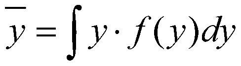
g) corrección de equivalencia de tejido vía el factor de escala usando la relación de poderes de frenado del tejido y del semiconductor: g) correction of tissue equivalence via the scale factor using the ratio of braking powers of the tissue and the semiconductor:
h) cálculo del equivalente de dosis estimada convolucionando los datos desde el apartado anterior con el factor de calidad, Q(LET) o Q(y) resumidos en tabla I [ICPR-36]: h) calculation of the estimated dose equivalent convolving the data from the previous section with the quality factor, Q (LET) or Q (y) summarized in Table I [ICPR-36]:
H = J- = = DTlssue Q{y)■ d{y)■ dy H = J - = = D Tlssue Q {y) ■ d {y) ■ dy
y J Tabla I. Factor de calidad Q(LET) and J Table I. Quality factor Q (LET)

i) estimación de la eficacia radiobiológica relativa RBE, según: i) estimate of the relative radiobiological efficacy RBE, according to:
RBE = ry 2f(y)Q(y)d[log(y)] RBE = r and 2 f (y) Q (y) d [log (y)]
J— Así, con la información final obtenida del RBE, puede estimarse los efectos radiobiológicos de la irradiación a nivel celular. J— Thus, with the final information obtained from the RBE, the radiobiological effects of irradiation at the cellular level can be estimated.
El dispositivo puede ser calibrado con fuentes radiactivas o haces de partículas de energías bien conocidas de manera que se deriva directamente la dosis depositada en el silicio por la radiación incidente. Para ello se acopla un sistema electrónico de lectura estándar a fin de que los pulsos de voltaje inducidos por el paso de la radiación en las celdas sean deconvolucionados a una lectura final de dosis equivalente (H). The device can be calibrated with radioactive sources or beams of well-known energy particles so that the dose deposited on the silicon by the incident radiation is directly derived. For this, a standard electronic reading system is coupled so that the voltage pulses induced by the passage of the radiation in the cells are deconvolved to a final equivalent dose reading (H).
Como ejemplo ilustrativo, cuando una partícula o radiación (201 ) atraviesa el microdosímetro produce pares e-h (203) que generarán finalmente un pulso de corriente. Dicho pulso es enviado a la electrónica de lectura (106) que contiene un preamplificador que integra el pulso de voltaje sobre el tiempo y genera una señal que es proporcional al número de pares e-h (203) depositada por la radiación en la celda; la electrónica de lectura (106) también contiene un shaping amplifier, que amplifica la señal que es después convertida en señal digital vía un conversor analógico-digital (ADC); posteriormente se registra para ser analizada por un pulse height analyzer. Así, gracias a esta cadena de tratamiento de datos, se infiere la cantidad de energía depositada por la radiación incidente en el sensor. As an illustrative example, when a particle or radiation (201) crosses the microdosimeter produces e-h pairs (203) that will ultimately generate a current pulse. Said pulse is sent to the reading electronics (106) which contains a preamplifier that integrates the voltage pulse over time and generates a signal that is proportional to the number of e-h pairs (203) deposited by the radiation in the cell; The reading electronics (106) also contain a shaping amplifier, which amplifies the signal that is then converted into a digital signal via an analog-to-digital converter (ADC); subsequently it is registered to be analyzed by a pulse height analyzer. Thus, thanks to this data processing chain, the amount of energy deposited by the incident radiation in the sensor is inferred.
Otro aspecto de la invención es el procedimiento para la fabricación del microdosímetro de la invención, que comprende las siguientes etapas: (a) Preparación del substrato del semiconductor (101 ) mediante procesos microelectrónicos o MEMS. En esta etapa se procede dependiendo del tipo de celda (205) (Figura 5 y 6): Another aspect of the invention is the process for manufacturing the microdosimeter of the invention, which comprises the following steps: (a) Preparation of the semiconductor substrate (101) by microelectronic or MEMS processes. This stage is followed depending on the type of cell (205) (Figure 5 and 6):
(a.1 ) Para la celda (205) tipo Figura 5: en primer lugar se procede a crear la componente central tipo P+ o N+ (104) por difusión o implantación. (a.1) For cell (205) type Figure 5: First, the central component type P + or N + (104) is created by diffusion or implantation.
(a.2) Para la celda (205) tipo Figura 6: se procede o bien a difundir o implantar una componente tipo P+ o N+ o bien a hacer un grabado cilíndrico-3D-anillo (602) de altura (605) que será llenado con polisilicio ya dopado o bien con polisilicio sin dopar y posteriormente éste será dopado tipo P+ o N+. (a.2) For cell (205) type Figure 6: either a P + or N + type component is disseminated or implanted or a cylindrical-3D-ring engraving (602) of height (605) is made, which will be filled with already doped polysilicon or with undoped polysilicon and later this will be doped type P + or N +.
(b) Grabado cilíndrico-3D en el semiconductor (101 ). (b) Cylindrical-3D engraving on the semiconductor (101).
Según sea la celda (205) que usemos (Figuras 5 y 6) se aplicará: (b.1 ) Para la celda (205) tipo Figura 5: se procede a realizar el grabado cilíndrico-3D (105) con forma de anillo, centrado en el píxel correspondiente a la celda, y después se llena con polisilicio dopado o con polisilicio sin dopar que posteriormente se dopa con dopante tipo N+ o P+ respectivamente (Figura 5). (b.2) Para la celda (205) tipo Figuras 6: se forma una columna cilíndrica-3D (601 ) en el centro de la celda, cuyas paredes internas también serán llenadas con polisilicio dopado o con polisilicio sin dopar que posteriormente se dopa con dopante tipo N+ o P+ respectivamente (Figura 6). (c) Creación de las metalizaciones (209) sobre (105) (en celda tipo Figuras 6) o (602) (en celda tipo Figuras 6), y la otra metalización de (210), sobre la componente central (104) o (601 ) respectiva e independientemente. La unión de sendas metalizaciones con sus correspondientes motivos P+ o N+ constituye los electrodos en sí de la celda. En el paso (c) las metalizaciones permiten la conexión con la electrónica de lectura (106) de la carga, pares e-h (203), que ha depositado la radiación o partículas incidentes (201 ) sobre la celda (205). Depending on the cell (205) that we use (Figures 5 and 6), the following will apply: (b.1) For cell (205), type Figure 5: the cylindrical-3D engraving (105) is performed as a ring, centered on the pixel corresponding to the cell, and then filled with doped polysilicon or undoped polysilicon which is then doped with a N + or P + type dopant respectively (Figure 5). (b.2) For the cell (205) type Figures 6: a cylindrical-3D column (601) is formed in the center of the cell, whose inner walls will also be filled with doped polysilicon or undoped polysilicon that is subsequently doped with dopante type N + or P + respectively (Figure 6). (c) Creation of the metallizations (209) on (105) (in cell type Figures 6) or (602) (in cell type Figures 6), and the other metallization of (210), on the central component (104) or (601) respectively and independently. The union of metallizations with their corresponding P + or N + motifs constitutes the electrodes themselves of the cell. In step (c) the metallizations allow the connection with the reading electronics (106) of the load, pairs e-h (203), which has deposited the radiation or incident particles (201) on the cell (205).
El proceso de grabado cilíndrico-3D se realiza preferentemente utilizando técnicas de ataque reactivo profundo con haz de iones (Deep Reactive Ion Etching o DRIE). Adicionalmente, parte de el volumen insensible de las obleas puede ser eliminado realizando un adelgazamiento del sustrato mediante procesos de grabado químico o ion reactivo, evitándose posibles contribuciones de retrodispersión o backscattering a la señal durante la irradiación de las partículas secundarias generadas en la irradiación, así se mejora la resolución energética, pues evita contribuciones alrededor del volumen sensible (208) que es la zona que eventualmente simulará la célula (Figuras 3 y 4). Esta configuración de microdosímetro está especialmente indicado en el caso de hadronterapia ya que los espesores de entre 2 μιη y 10 μιη (inferiores a los espesores de las obleas convencionales) son adecuados para las partículas pesadas usadas en hadronterapia, e.g. Iones de carbono, helio, neón, litio, silicio, etc. En radioterapia un bajo espesor de los detectores (109) no sería muy adecuado pues la detección de las partículas de radioterapia (fotones) sería muy baja debido a que la absorción de fotones es proporcional al volumen del semiconductor (101 ). Otro objeto de la invención es el uso del microdosímetro de la invención para detección de radiación en el campo de la aplicación médica, preferentemente en hadronterapia donde es necesario detectar protones e iones de carbono principalmente El microdosímetro puede realizar tanto medidas a nivel superficial, e.g. superficie de la piel o interfaz biológica, o a una cierta profundidad, e.g. debajo de la piel o el tejido irradiado. The cylindrical-3D etching process is preferably performed using deep reactive attack techniques with ion beam (Deep Reactive Ion Etching or DRIE). Additionally, part of the wafer insensitive volume can be eliminated by thinning the substrate by chemical etching or reactive ion processes, avoiding possible backscattering or backscattering contributions to the signal during irradiation of the secondary particles generated in the irradiation, thus The energy resolution is improved, as it avoids contributions around the sensitive volume (208), which is the area that will eventually simulate the cell (Figures 3 and 4). This microdosimeter configuration is especially indicated in the case of hadronterapia since the thicknesses between 2 μιη and 10 μιη (lower than the thicknesses of conventional wafers) are suitable for heavy particles used in hadronterapia, eg carbon ions, helium, neon, lithium, silicon, etc. In radiotherapy a low thickness of the detectors (109) would not be very suitable since the detection of the radiotherapy particles (photons) would be very low because the photon absorption is proportional to the volume of the semiconductor (101). Another object of the invention is the use of the microdosimeter of the invention for detection of radiation in the field of medical application, preferably in hadronterapia where it is necessary to detect protons and carbon ions mainly. The microdosimeter can perform both surface level measurements, eg surface from the skin or biological interface, or at a certain depth, eg under the skin or irradiated tissue.
Además de su uso directo en aplicaciones de microdosimetría en hadronterapia ex/in-vivo, el microdosímetro de la invención puede ir acoplado a un material equivalente a tejido que simulase tejido biológico específico, por ejemplo agua, músculo, hueso, etc, a fin de que éste genere las partículas -debido a la ionización del haz primario en el tejido-equivalente- que el microdosímetro puede a su vez detectar mediante el procedimiento de la invención, para efectuar otros estudios dosimétricos de investigación. De esta forma podría parametrizarse los campos usados en radio/hadron terapia, así como otros campos derivados de otros entornos de radiación, e.g. neutrones secundarios generados en dichas terapias. El microdosímetro puede utilizarse en otros campos derivados de otros entornos de radiación, como neutrones secundarios generados en radio/hadron terapia. In addition to its direct use in applications of microdosimetry in ex-in-vivo hadronterapia, the microdosimeter of the invention can be coupled to a tissue equivalent material that simulates specific biological tissue, for example water, muscle, bone, etc., in order to that the latter generates the particles - due to the ionization of the primary beam in the tissue-equivalent - that the microdosimeter can in turn detect by means of the method of the invention, to carry out other dosimetric research studies. In this way the fields used in radio / hadron therapy could be parameterized, as well as other fields derived from other radiation environments, e.g. secondary neutrons generated in these therapies. The microdosimeter can be used in other fields derived from other radiation environments, such as secondary neutrons generated in radio / hadron therapy.
Adicionalmente se pueden incluir su uso campos mixtos de radiación acoplando una matriz de múltiples microdosímetros de forma tal que cada uno de ellos sea más sensible a cada tipo de radiación (en un campo de radiación mixto). Este campo incluye protección radiológica en uso personal y monitorización de área, para sistema portátiles, hadronterapia y en el campo de la aplicación aerospacial, como por ejemplo detección de partículas cósmicas cargadas de alta energía. Additionally, mixed radiation fields can be included using a matrix of multiple microdosimeters so that each of them is more sensitive to each type of radiation (in a mixed radiation field). This field includes radiation protection in personal use and area monitoring, for portable systems, hadronterapia and in the field of aerospace application, such as detection of high energy charged cosmic particles.
DESCRIPCIÓN FIGURAS: DESCRIPTION FIGURES:
Figura 1. Diferentes geometrías y sustratos del microdosímetro de la invención A)Figure 1. Different geometries and substrates of the microdosimeter of the invention A)
Esquema de la sección transversal de microdosímetro fabricado en oblea tipo Semiconductor-on-lnsulator (SOI) B) Esquema tridimensional de A C) Esquema de la sección transversal de microdosímetro fabricado en una oblea de silicio estándar D) Esquema tridimensional de C. Diagram of the cross section of the microdosimeter manufactured in Wafer type Semiconductor-on-lnsulator (SOI) B) Three-dimensional scheme of A C) Diagram of the cross-section of the microdosimeter manufactured in a standard silicon wafer D) Three-dimensional scheme of C.
Figura 2. Equivalencia del funcionamiento de la célula biológica y celda del microdosímetro de la invención. A) Esquema de célula biológica B) Ejemplo de celda de la invención C) Esquema de la vista transversal de la celda de B. Figure 2. Equivalence of the functioning of the biological cell and microdosimeter cell of the invention. A) Biological cell scheme B) Example of cell of the invention C) Diagram of the cross-sectional view of cell B.
Figura 3. Microdosímetro sobre oblea SOI con sustrato adelgazado Figure 3. Microdosimeter on SOI wafer with thinned substrate
A) Sección transversal B) Esquema tridimensional. A) Cross section B) Three-dimensional scheme.
Figura 4. Microdosímetro sobre oblea de silicio con sustrato adelgazado A) Sección transversal en proceso de adelgazamiento B) Sección transversal ya adelgazado. Figure 4. Microdosimeter on silicon wafer with thinned substrate A) Cross section in thinning process B) Cross section already thinned.
Figura 5. Celda tipo grabado cilíndrico-3D-anillo. Esquema superior: esquema tridimensional . Figura central: sección transversal de dicha celdas con difusión o implantación central tipo P+ rodeado de grabado cilíndrico-3D tipo N+. Esquema inferior: idem que superior pero con dopajes (P+ o N+) invertidos. Figure 5. Cylindrical-3D-ring engraved type cell. Upper scheme: three-dimensional scheme. Central figure: cross section of said cells with diffusion or central implantation type P + surrounded by cylindrical-3D engraving type N +. Lower scheme: idem than superior but with doping (P + or N +) inverted.
Figura 6. Celda tipo grabado cilíndrico-3D-columna: Esquema superior: esquema tridimensional. Figura central e inferior : representación de una celda con grabado cilíndrico- 3D-columna, cuyas paredes interna se dopa tipo P+/N+ y está rodeado por un anillo de implantación N+/P+ respectivamente. Figure 6. Cylindrical-3D-column engraved type cell: Upper scheme: three-dimensional scheme. Central and lower figure: representation of a cell with cylindrical-3D-column engraving, whose internal walls are doped type P + / N + and is surrounded by an implantation ring N + / P + respectively.
Figura 7. Esquema de la conexión de la electrónica de lectura del microdosímetro con lectura continua Figura 8. Esquema de la conexión de la electrónica de lectura del microdosímetro con lectura independiente . Figura 9. Modelo de distribución de campo en el interior de la celda limitada por anillo cilindrico. A) Distribución de campo eléctrico B) Distribución de potencial C) Curvas intensidad voltaje D) Curvas capacidad voltaje. Fig. 10a. Croquis de la disposición de un microsensor (no a escala) del ejemplo 4. Los agujeros de tipo n y de tipo p están conectados con líneas de metal. Figure 7. Diagram of the connection of the reading electronics of the microdosimeter with continuous reading Figure 8. Diagram of the connection of the reading electronics of the microdosimeter with independent reading. Figure 9. Field distribution model inside the cell limited by cylindrical ring. A) Electric field distribution B) Potential distribution C) Voltage intensity curves D) Voltage capacity curves. Fig. 10a. Sketch of the arrangement of a microsensor (not to scale) of example 4. The holes of type n and of type p are connected with metal lines.
Fig. 10b. Esquema de dos microsensores del ejemplo 4 a una distancia P. Fig. 11 a. Imagen SEM de la vista superior de un microdosímetro con 9 μιη de diámetro, 100 μιη de campo y 6 μιη de espesor, descrito en el ejemplo 4. Fig. 10b. Scheme of two microsensors of example 4 at a distance P. Fig. 11 a. SEM image of the top view of a microdosimeter with 9 μιη diameter, 100 μιη field and 6 μιη thickness, described in example 4.
Fig. 11 . Imagen SEM de la vista superior de un microsensor fabricado igual al diseñado en la figura 11 a. Fig. 11. SEM image of the top view of a fabricated microsensor equal to that designed in Figure 11 a.
Fig. 12. Curva característica de tensión de algunos microdosímetros de tipo pista en una de las obleas fabricadas, descritos en el ejemplo 4. Fig. 12. Tension characteristic curve of some track type microdosimeters in one of the wafers manufactured, described in example 4.
MODO DE REALIZACIÓN DE LA INVENCIÓN EMBODIMENT OF THE INVENTION
Ejemplo 1. En este ejemplo se muestra la estructura/fabricación de un microdosímetro sobre oblea SOI Example 1. This example shows the structure / manufacture of a SOI wafer microdosimeter
El material de base son obleas SOI con silicio activo de tipo N, de alta resistividad y de grosor (109) entre 1 μιη y 100 μιη. Después de una limpieza estándar (RCA u otro) se crece un óxido de silicio térmico para pasivar la superficie del silicio. The base material is SOI wafers with active silicon type N, high resistivity and thickness (109) between 1 μιη and 100 μιη. After a standard cleaning (RCA or other) a thermal silicon oxide is grown to passivate the silicon surface.
En la parte superior de la oblea, se abre una pequeña ventana circular, por ejemplo de 4 μιη de diámetro, en el óxido de silicio por grabado ión-reactivo o grabado húmedo. Se implanta o difunde entonces el silicio con boro u otro dopante de tipo P para crear un contacto P+, de la unión PN. El grabado cilíndrico-3D en forma de anillo (105) (de anchura típica 3 μιη), y centrado en los contactos P+ anteriores, se graba en el silicio activo por grabado ión- reactivo profundo DRIE (con el proceso Bosch por ejemplo) hasta el óxido enterrado. Se deposita polisilicio por técnicas de depósito químico en fase vapor u otra técnica de depósito conformal. Este material se dopa con fósforo u otro dopante de tipo N, durante el depósito o después de aquel, para crear un contacto óhmico en las paredes del grabado cilíndrico-3D en forma de anillo. El polisilicio se define mediante fotolitografía y se graba para formar contactos separados alrededor del anillo. Se deposita por depósito químico de fase vapor un dieléctrico intermetal de espesor típico de 1 μηι y compuesto de óxido de silicio, nitruro de silicio u otro dieléctrico apropiado para la protección de los agujeros de los procesos siguientes. En este dieléctrico se graban vías hasta los contactos P+ y N+ por grabado ión-reactivo o grabado húmedo. At the top of the wafer, a small circular window, for example 4 μιη in diameter, is opened in silicon oxide by ion-reactive etching or wet etching. The silicon is then implanted or diffused with boron or other P-type dopant to create a P + contact, of the PN junction. The cylindrical-3D ring-shaped engraving (105) (of typical width 3 μιη), and centered on the previous P + contacts, is etched on the active silicon by deep-reactive ion-reactive etching DRIE (with the Bosch process for example) up to the buried rust. Polysilicon is deposited by chemical vapor deposition techniques or other conformal deposition technique. This material is doped with phosphorus or other type N dopant, during deposit or after that, to create an ohmic contact on the walls of the cylindrical-3D ring-shaped engraving. The polysilicon is defined by photolithography and is recorded to form separate contacts around the ring. An intermetal dielectric with a typical thickness of 1 μηι and composed of silicon oxide, silicon nitride or other dielectric suitable for the protection of the holes of the following processes is deposited by vapor phase chemical deposit. In this dielectric, pathways to the P + and N + contacts are recorded by ion-reactive etching or wet etching.
Para definir las líneas de interconexión y los pads para la conexión, que puede ser realizada mediante hilado ultrasónico (wirebonding) se deposita aluminio por depósito físico de fase vapor y se define por grabado ión-reactivo o grabado húmedo. Por último para abrir los pads de wirebonding en aluminio.se deposita por depósito químico de vapores asistido por plasma una pasivación, por ejemplo una bicapa de óxido de silicio y nitruro de silicio que se define por grabado ión-reactivo. To define the interconnection lines and the pads for the connection, which can be done by ultrasonic spinning (wirebonding) aluminum is deposited by physical vapor phase deposit and is defined by ion-reactive etching or wet etching. Finally, to open the wirebonding pads in aluminum, a passivation, for example a silicon oxide and silicon nitride bilayer which is defined by ion-reactive etching, is deposited by chemical vapor deposition assisted by plasma.
Hay un total de 100 celdas unidad de 80 x 80 μιη2 y el área sensible total del microdosímetro es de ~1 mm2. There is a total of 100 unit cells of 80 x 80 μιη 2 and the total sensitive area of the microdosimeter is ~ 1 mm 2 .
Ejemplo 2. Estructura del microdosímetro adecuada para hadronterapia Example 2. Structure of the microdosimeter suitable for hadronterapia
Se procede como en el caso anterior pero las capas de silicio no sensible (103) o (405) en el dorso de la oblea se graban para formar una ventana cuya área corresponde al área activa del sensor. En el caso de obleas de silicio, se trata el silicio de la parte posterior de la oblea con grabado ión-reactivo o grabado húmedo hasta alcanzar el óxido enterrado. De esta manera se produce un sustrato adelgazado. Proceed as in the previous case but the layers of non-sensitive silicon (103) or (405) on the back of the wafer are engraved to form a window whose area corresponds to the active area of the sensor. In the case of silicon wafers, the silicon on the back of the wafer is treated with ion-reactive etching or wet etching until the buried oxide is reached. In this way a thinned substrate is produced.
La irradiación puede realizarse indistintamente tanto por la cara superior del microdosímetro como por la inferior. Puesto que (107) y (109) son 10 μιη respectivamente, la celda es un cilindro con diámetro igual a su altura. Irradiation can be performed interchangeably both on the upper face of the microdosimeter and on the lower side. Since (107) and (109) are 10 μιη respectively, the cell is a cylinder with a diameter equal to its height.
Ejemplo 3: Modelo de estructura de la unión PN fabricada con grabado cilindrico 3D y procesos tecnológicos que muestra su viabilidad como microdosímetro. Example 3: Structure model of the PN junction manufactured with 3D cylindrical engraving and technological processes that shows its viability as a microdosimeter.
Modelo de funcionamiento realizado con el software de simulación eléctrica de dispositivos semiconductores "SENTAURUS" (Synopsys TCAD Sentaurus , a finite element semiconductor simulation package, referencia: Synopsys TCAD Sentaurus, http://www.svnopsvs.com/tools/tcad/Paqes/default.aspx a 12 de Diciembre de 2013 ). Operating model performed with the "SENTAURUS" semiconductor electrical simulation software (Synopsys TCAD Sentaurus, a finite element semiconductor simulation package, reference: Synopsys TCAD Sentaurus, http://www.svnopsvs.com/tools/tcad/Paqes/default.aspx as of December 12, 2013).
Las figura 9A y 9B muestran la distribución de campo eléctrico y de potencial en una celda. El ejemplo de esta geometría en ambas figuras se refiere a una celda como la definida en la figura 5, con un diámetro (112) del motivo (104) de 20 μιη y un diámetro (113) del motivo (105) de 5 μιη y un diámetro (107) del volumen-sensible de 70 μιη. La unión PN ahí diseñada (creada entre (104) y (105)) a través de las metalizaciones (209) y (210) dan lugar a un campo eléctrico. En las figuras 9 A y 9B se observa cómo se logra el vaciado del volumen-sensible (208) total y dicho volumen sensible (208) tiene una forma cilindrica bien delimitada geométricamente que simula la estructura y/o subestructura celular. Al lograr el vaciamiento total del volumen sensible, se indica que al pasar una partícula cargada (201 ), e.g. protón o ión de carbón como los usados en hadronterapia, todos los pares electrón- hueco (e-h) (203) que genera a su paso, ionizando el medio del volumen-sensible (208), llegan a los contactos metálicos (209 y 210) y producirán la señal que es leída por la electrónica de lectura (106). Figures 9A and 9B show the distribution of electric field and potential in a cell. The example of this geometry in both figures refers to a cell as defined in Figure 5, with a diameter (112) of the motif (104) of 20 μιη and a diameter (113) of the motif (105) of 5 μιη and a diameter (107) of the volume-sensitive of 70 μιη. The PN junction designed there (created between (104) and (105)) through the metallizations (209) and (210) give rise to an electric field. In Figures 9 A and 9B it is observed how the emptying of the total sensitive volume (208) is achieved and said sensitive volume (208) has a well defined geometrically cylindrical shape that simulates the cellular structure and / or substructure. When achieving total emptying of the sensitive volume, it is indicated that when passing a charged particle (201), e.g. proton or carbon ion like those used in hadronterapia, all the electron-hollow pairs (eh) (203) that it generates in its path, ionizing the volume-sensitive medium (208), reach the metal contacts (209 and 210) and will produce the signal that is read by the reading electronics (106).
Toda los pares e-h (203) son netamente recolectados en los contactos metálicos (209 y 210) y por lo tanto la eficiencia de colección de carga (CCE) es del 100%. Es decir, que toda la energía depositada por radiación ionizante, ε, será totalmente medida por el volumen- sensible (208). Éste es un requisito indispensable para evaluar directamente la energía total de la radiación incidente, puesto que si la CCE no es del 100%, la energía lineal, ε, no es un valor fidedigno y por lo tanto las magnitudes derivadas no serían reales. Las figuras 9C y 9D representan las curvas de caracterización eléctrica derivadas de las anteriores simulaciones, las curvas intensidad-voltaje IV y capacidad-voltaje CV respectivamente. En la IV se ve que cada celda (208) así diseñada tendría todo su volumen- sensible con vaciamiento completo cuando se aplican 20 V en (206) y que la corriente inversa teórica es baja All e-h pairs (203) are clearly collected at the metal contacts (209 and 210) and therefore the charge collection efficiency (CCE) is 100%. That is, all the energy deposited by ionizing radiation, ε, will be totally measured by the volume-sensitive (208). This is an indispensable requirement to directly evaluate the total energy of the incident radiation, since if the CCE is not 100%, the linear energy, ε, is not a reliable value and therefore the derived quantities would not be real. Figures 9C and 9D represent the electrical characterization curves derived from the previous simulations, the intensity-voltage curves IV and capacity-voltage CV respectively. In IV it is seen that each cell (208) thus designed would have its full volume-sensitive with full emptying when 20 V is applied in (206) and that the theoretical inverse current is low
(< 1 e"12 A ), i.e. buena para su funcionamiento posterior. En la figura 9C se ve que a 20 V la capacidad en vaciamiento completo es inferior a 10e"15 F. Estos valores muestran que, primero éste es un dispositivo de "bajo consumo", respecto a otros citados en el estado del arte, como las cámaras de ionización, que necesitan decenas de V para funcionar y segundo que el ruido intrínseco es muy bajo. (<1 e "12 A), ie good for later operation. Figure 9C shows that at 20 V the capacity for complete emptying is less than 10e " 15 F. These values show that, first this is a device of "low consumption", compared to others cited in the state of the art, such as ionization chambers, which need tens of V to operate and second that the intrinsic noise is very low.
Ejemplo 4. Microdosímetros de silicio basados en diodos cilindricos. Se ha desarrollado un nuevo microdosímetro como el detector de base para las aplicaciones microdosimétricas. Estos dispositivos se fabrican en tres tipos de obleas de SOÍ con un sustrato de tipo n alta resistividad y con volúmenes activos de 6, 10 y 20 μιη de espesor, para cada tipo de oblea. Los electrodos colectores son columnas grabadas a través del silicio en lugar de ser implantes de superficie como en los diodos planos estándar, lo que permite una capacidad mucho menor y por lo tanto un ruido electrónico inferior en comparación con un sensor plano del mismo espesor. Los sensores están fabricados en instalaciones de sala blanca. La Figura 10 muestra la disposición esquemática de estos microdosímetros donde se muestran ios p-n electrodos y las tiras de metal que los conectan con ios contactos: el p-electrodo tienen un diámetro de 4 μιη y está rodeado de agujeros-n anillo de 3 μιη de espesor con 6, 10 y 20 μιη de profundidad (para cada tipo de oblea) distribuido en una geometría cuadrada. Una oblea contiene microdosímetros con emplazamientos de 25, 50, 100 y 200 μιη (siendo P la distancia entre p-columnas) y con un diámetro interno (D) de 9, 10, 15, 20 y 25 μιη, con el fin de incluir un mayor número de distribución de celdas y tamaños. El electrodo de tipo p es circular y se ha llevado a cabo una implantación iónica con boro (p+). Un anillo cilindrico se graba utilizando la técnica de grabado profundo por iones reactivos (DRIE), para después ser llenado parcialmente con polisilicio dopado con fósforo (n+) para formar la unión p-n. La parte superior de ios agujeros está metalizada con aluminio y cada electrodo está conectado con una línea de aluminio para proporcionar el contacto eléctrico. Example 4. Silicon microdosimeters based on cylindrical diodes. A new microdosimeter has been developed as the base detector for microdosimetric applications. These devices are manufactured in three types of SOÍ wafers with a substrate of type n high resistivity and with active volumes of 6, 10 and 20 μιη thickness, for each type of wafer. The collector electrodes are columns recorded through silicon instead of being surface implants as in standard flat diodes, which allows for a much smaller capacity and therefore a lower electronic noise compared to a flat sensor of the same thickness. The sensors are manufactured in cleanroom facilities. Figure 10 shows the schematic arrangement of these microdosimeters showing the pn electrodes and the metal strips that connect them to the contacts: the p-electrode has a diameter of 4 μιη and is surrounded by n-ring holes of 3 μιη thickness with 6, 10 and 20 μιη depth (for each type of wafer) distributed in a square geometry. A wafer contains microdosimeters with locations of 25, 50, 100 and 200 μιη (where P is the distance between p-columns) and with an internal diameter (D) of 9, 10, 15, 20 and 25 μιη, in order to include a greater number of distribution of cells and sizes. The p-type electrode is circular and an ion implantation with boron (p +) has been carried out. A cylindrical ring is etched using the technique of deep etching by reactive ions (DRIE), and then partially filled with phosphorus doped polysilicon (n +) to form the pn junction. The top of the holes is metallized with aluminum and each electrode is connected with an aluminum line to provide electrical contact.
Cada microdosímetro consta de 121 microsensores independientes dispuestos en una matriz cuadrada. Se desarrollaron tres tipos principales de estructuras de detectores: detector de pista (detector de pixel-array), detector de tira y detector de pixel. La configuración más sencilla es la de detector de pista en el que todos ios electrodos n+ están conectados al contacto n+ en un lado del sensor, mientras que todos ios electrodos p+ se conectan al contacto p+ en el lado opuesto, recogiendo de este modo toda la carga en todas las celdas de la unidad o volúmenes sensibles. En la configuración de la tira, los electrodos de tipo p consecutivos se alinean, lo que resulta en una franja de microsensores conectados en una fila. En la configuración de píxeles, aunque suela ser usual utilizar bump-bonded para la lectura del chip electrónico según la técnica fiip-chip, en este diseño cada microsensor se enruta a través de una línea de metal a una almohadilla de conexión para la lectura de microtiras electrónicas para hacer la lectura más fácil. Grabando con golpeteo el soporte de silicio de la oblea SO! desde e! lado posterior en este lado, se espera que se obtengan microsensores más finos para las tres configuraciones antes mencionadas. La Figura 11 muestra dos imágenes SEM de una obiea procesada que contiene algunos microsensores de píxeles. Each microdosimeter consists of 121 independent microsensors arranged in a square matrix. Three main types of detector structures were developed: track detector (pixel-array detector), strip detector and pixel detector. The simplest configuration is the track detector in which all the n + electrodes are connected to the n + contact on one side of the sensor, while all the p + electrodes are connected to the p + contact on the opposite side, thus collecting all the load in all unit cells or sensitive volumes. In the strip configuration, the consecutive p-type electrodes are aligned, resulting in a strip of microsensors connected in a row. In the pixel configuration, although it is usual to use bump-bonded for reading the electronic chip according to the fiip-chip technique, in this design each microsensor is routed through a metal line to a connecting pad for reading electronic microtira to make reading easier. Tapping the wafer silicon support SO! from e! back side on this side, it is expected that finer microsensors will be obtained for the three configurations mentioned above. The Figure 11 shows two SEM images of a processed obiea that contains some pixel microsensors.
Los microdosímetros están conectados a un sistema de electrónica de lectura apropiada para llevar a cabo las pruebas experimentales. Los resultados de la caracterización eléctrica de los primeros prototipos de tipo pista se desglosan a continuación. The microdosimeters are connected to an appropriate electronic reading system to carry out the experimental tests. The results of the electrical characterization of the first track-type prototypes are detailed below.
Una prueba de funcionamiento inicial se llevó a cabo en la obiea. Las características de corriente frente a tensión inversa de los diodos fabricados se obtuvieron con una estación de sonda semiautomática y un Analizador de Parámetro Semiconductor HP4155. La Figura 12 muestra los resultados para algunos microsensores de tipo pista. Estos microdosímetros de tipo almohadilla tienen un canal de lectura, una superficie total de 2000 x 2625 im2 y sus microsensores se distribuyen en una cuadrícula de 11 x 11 píxeles. Las curvas I-V muestran un comportamiento típico del diodo. Los dispositivos son totalmente funcionales, ya que pueden estar predispuestos para revertir las tensiones superiores a agotamiento completo (<1V) y las corrientes de fuga son bajas. An initial function test was carried out on the obiea. The current versus reverse voltage characteristics of the manufactured diodes were obtained with a semi-automatic probe station and an HP4155 Semiconductor Parameter Analyzer. Figure 12 shows the results for some track type microsensors. These pad-type microdosimeters have a reading channel, a total area of 2000 x 2625 im 2 and their microsensors are distributed in an 11 x 11 pixel grid. IV curves show a typical diode behavior. The devices are fully functional, as they may be predisposed to reverse voltages higher than complete exhaustion (<1V) and leakage currents are low.
En resumen, los microdosímetros innovadores descritos anteriormente basados en las estructuras 3D-cilíndricas con 8, 10 y 20 pm de espesor, y las dimensiones y campos variables, es decir, 9, 10, 15, 20 25 m de diámetro interno y con emplazamientos de 25, 50, 100 y 200 \¡ , han sido exitosamente fabricados. Estos primera generación de microdosimeters de tipo pista sobre la base de una estructura 3D cilindrica optimizada para crear microsensores muestra la viabilidad para bajar hasta el nivel del tamaño de celda promedio, y proporcionando así una medición más cercana del AE de silicio. In summary, the innovative microdosimeters described above based on 3D-cylindrical structures with 8, 10 and 20 pm thickness, and variable dimensions and fields, that is, 9, 10, 15, 20 25 m internal diameter and with locations 25, 50, 100 and 200, have been successfully manufactured. These first generation of track-type microdosimeters based on a cylindrical 3D structure optimized to create microsensors shows the feasibility of lowering to the level of the average cell size, and thus providing a closer measurement of silicon AE.
El uso de estos microdosímetros 3D podría mejorar la exactitud de ios cálculos RBE normalmente afectados por la incertidumbre inherente de simulaciones de Monte Cario, debido a la aproximación de la composición del material y las leyes físicas dependientes de la energía involucrada en estos cálculos. The use of these 3D microdosimeters could improve the accuracy of the RBE calculations normally affected by the inherent uncertainty of Monte Cario simulations, due to the approximation of the material composition and the energy-dependent physical laws involved in these calculations.
Claims


Applications Claiming Priority (2)
| Application Number | Priority Date | Filing Date | Title |
|---|---|---|---|
| ES201430099 | 2014-01-28 | ||
| ESP201430099 | 2014-01-28 |
Publications (1)
| Publication Number | Publication Date |
|---|---|
| WO2015114193A1 true WO2015114193A1 (en) | 2015-08-06 |
Family
ID=53756259
Family Applications (1)
| Application Number | Title | Priority Date | Filing Date |
|---|---|---|---|
| PCT/ES2015/070056 Ceased WO2015114193A1 (en) | 2014-01-28 | 2015-01-28 | Microdosimeter based on 3d semiconductor structures, method for producing said microdosimeter, and use of said microdosimeter |
Country Status (1)
| Country | Link |
|---|---|
| WO (1) | WO2015114193A1 (en) |
Citations (1)
| Publication number | Priority date | Publication date | Assignee | Title |
|---|---|---|---|---|
| US20100090118A1 (en) * | 2006-12-19 | 2010-04-15 | University Of Wollongong | Method and apparatus for tissue equivalent solid state microdosimetry |
-
2015
- 2015-01-28 WO PCT/ES2015/070056 patent/WO2015114193A1/en not_active Ceased
Patent Citations (1)
| Publication number | Priority date | Publication date | Assignee | Title |
|---|---|---|---|---|
| US20100090118A1 (en) * | 2006-12-19 | 2010-04-15 | University Of Wollongong | Method and apparatus for tissue equivalent solid state microdosimetry |
Non-Patent Citations (3)
| Title |
|---|
| GARCIA F ET AL.: "A novel ultra-thin 3D detector- For plasma diagnostics at JET and ITER tokamaks.", NUCLEAR INSTRUMENTS & METHODS IN PHYSICS RESEARCH. SECTION A., vol. 607, no. 1, 1 August 2009 (2009-08-01), pages 57 - 60, XP026320944 * |
| LIM, W. H. ET AL.: "Cylindrical Silicon-on-Insulator Microdosimeter: Design, Fabrication and TCAD Modeling.", IEEE TRANSACTIONS ON NUCLEAR SCIENCE, vol. 56, no. 2, pages 424 - 428, XP011255135 * |
| ZIEBELL, A. L. ET AL.: "A Cylindrical Silicon-on-Insulator Microdosimeter: Charge Collection Characteristics.", IEEE TRANSACTIONS ON NUCLEAR SCIENCE, vol. 55, no. 6, 1 December 2008 (2008-12-01), pages 3414 - 3420, XP011240759 * |
Similar Documents
| Publication | Publication Date | Title |
|---|---|---|
| Rosenfeld | Novel detectors for silicon based microdosimetry, their concepts and applications | |
| US8421022B2 (en) | Method and apparatus for tissue equivalent solid state microdosimetry | |
| Tran et al. | 3D-Mesa “Bridge” Silicon Microdosimeter: Charge Collection Study and Application to RBE Studies in $^{12}{\rm C} $ Radiation Therapy | |
| US9941440B2 (en) | Radiation microdosimeters correlated with biological cells and cell components | |
| Parisi et al. | Microdosimetry for hadron therapy: a state of the art of detection technology | |
| Amaldi et al. | Construction, test and operation of a proton range radiography system | |
| Petasecca et al. | Angular independent silicon detector for dosimetry in external beam radiotherapy | |
| Prieto-Pena et al. | Microdosimetric spectra measurements on a clinical carbon beam at nominal therapeutic fluence rate with silicon cylindrical microdosimeters | |
| Guardiola et al. | Silicon-based three-dimensional microstructures for radiation dosimetry in hadrontherapy | |
| Pastuovic et al. | IBIC microscopy–The powerful tool for testing micron–Sized sensitive volumes in segmented radiation detectors used in synchrotron microbeam radiation and hadron therapies | |
| Kok et al. | Fabrication and first characterization of silicon-based full 3-D microdosimeters | |
| Bachiller-Perea et al. | Characterization of the charge collection efficiency in silicon 3-D-detectors for microdosimetry | |
| Mendicino et al. | Characterization of 3D and planar Si diodes with different neutron converter materials | |
| Ziebell et al. | A cylindrical silicon-on-insulator microdosimeter: Charge collection characteristics | |
| Tran et al. | Ultra-thin 3-D detector: Charge collection characterization and application for microdosimetry | |
| WO2015114193A1 (en) | Microdosimeter based on 3d semiconductor structures, method for producing said microdosimeter, and use of said microdosimeter | |
| Jakubek et al. | 3D imaging of radiation damage in silicon sensor and spatial mapping of charge collection efficiency | |
| EP3933449B1 (en) | System for dosimetric and micro-dosimetric ionizing radiation characterization | |
| Bachiller-Perea et al. | Multi-arrays of 3D cylindrical microdetectors for beam characterization and microdosimetry in proton therapy | |
| Kanxheri et al. | Intercalibration of a polycrystalline 3D diamond detector for small field dosimetry | |
| Guardiola et al. | First silicon microdosimeters based on cylindrical diodes | |
| Cayley et al. | Playing Hard with Si: Challenges and Opportunities for New Materials in Radiation Therapy Dosimetry | |
| Caffrey et al. | Space radiation dosimetry: overview and recent developments | |
| Ziebell et al. | Cylindrical silicon-on-insulator microdosimeter: Charge collection characteristics | |
| Tran et al. | 3D bridge microdosimeter: Charge collection study and application to RBE studies in 12C radiation therapy |
Legal Events
| Date | Code | Title | Description |
|---|---|---|---|
| 121 | Ep: the epo has been informed by wipo that ep was designated in this application |
Ref document number: 15743363 Country of ref document: EP Kind code of ref document: A1 |
|
| NENP | Non-entry into the national phase |
Ref country code: DE |
|
| 122 | Ep: pct application non-entry in european phase |
Ref document number: 15743363 Country of ref document: EP Kind code of ref document: A1 |