WO2015114720A1 - Procédé d'inspection d'un panneau d'affichage électroluminescent organique et appareil d'inspection d'un panneau d'affichage électroluminescent organique - Google Patents
Procédé d'inspection d'un panneau d'affichage électroluminescent organique et appareil d'inspection d'un panneau d'affichage électroluminescent organique Download PDFInfo
- Publication number
- WO2015114720A1 WO2015114720A1 PCT/JP2014/006351 JP2014006351W WO2015114720A1 WO 2015114720 A1 WO2015114720 A1 WO 2015114720A1 JP 2014006351 W JP2014006351 W JP 2014006351W WO 2015114720 A1 WO2015114720 A1 WO 2015114720A1
- Authority
- WO
- WIPO (PCT)
- Prior art keywords
- display panel
- shutter
- organic
- pixels
- display
- Prior art date
- Legal status (The legal status is an assumption and is not a legal conclusion. Google has not performed a legal analysis and makes no representation as to the accuracy of the status listed.)
- Ceased
Links
Images





Classifications
-
- G—PHYSICS
- G09—EDUCATION; CRYPTOGRAPHY; DISPLAY; ADVERTISING; SEALS
- G09G—ARRANGEMENTS OR CIRCUITS FOR CONTROL OF INDICATING DEVICES USING STATIC MEANS TO PRESENT VARIABLE INFORMATION
- G09G3/00—Control arrangements or circuits, of interest only in connection with visual indicators other than cathode-ray tubes
- G09G3/20—Control arrangements or circuits, of interest only in connection with visual indicators other than cathode-ray tubes for presentation of an assembly of a number of characters, e.g. a page, by composing the assembly by combination of individual elements arranged in a matrix no fixed position being assigned to or needed to be assigned to the individual characters or partial characters
- G09G3/22—Control arrangements or circuits, of interest only in connection with visual indicators other than cathode-ray tubes for presentation of an assembly of a number of characters, e.g. a page, by composing the assembly by combination of individual elements arranged in a matrix no fixed position being assigned to or needed to be assigned to the individual characters or partial characters using controlled light sources
- G09G3/30—Control arrangements or circuits, of interest only in connection with visual indicators other than cathode-ray tubes for presentation of an assembly of a number of characters, e.g. a page, by composing the assembly by combination of individual elements arranged in a matrix no fixed position being assigned to or needed to be assigned to the individual characters or partial characters using controlled light sources using electroluminescent panels
- G09G3/32—Control arrangements or circuits, of interest only in connection with visual indicators other than cathode-ray tubes for presentation of an assembly of a number of characters, e.g. a page, by composing the assembly by combination of individual elements arranged in a matrix no fixed position being assigned to or needed to be assigned to the individual characters or partial characters using controlled light sources using electroluminescent panels semiconductive, e.g. using light-emitting diodes [LED]
- G09G3/3208—Control arrangements or circuits, of interest only in connection with visual indicators other than cathode-ray tubes for presentation of an assembly of a number of characters, e.g. a page, by composing the assembly by combination of individual elements arranged in a matrix no fixed position being assigned to or needed to be assigned to the individual characters or partial characters using controlled light sources using electroluminescent panels semiconductive, e.g. using light-emitting diodes [LED] organic, e.g. using organic light-emitting diodes [OLED]
- G09G3/3225—Control arrangements or circuits, of interest only in connection with visual indicators other than cathode-ray tubes for presentation of an assembly of a number of characters, e.g. a page, by composing the assembly by combination of individual elements arranged in a matrix no fixed position being assigned to or needed to be assigned to the individual characters or partial characters using controlled light sources using electroluminescent panels semiconductive, e.g. using light-emitting diodes [LED] organic, e.g. using organic light-emitting diodes [OLED] using an active matrix
- G09G3/3233—Control arrangements or circuits, of interest only in connection with visual indicators other than cathode-ray tubes for presentation of an assembly of a number of characters, e.g. a page, by composing the assembly by combination of individual elements arranged in a matrix no fixed position being assigned to or needed to be assigned to the individual characters or partial characters using controlled light sources using electroluminescent panels semiconductive, e.g. using light-emitting diodes [LED] organic, e.g. using organic light-emitting diodes [OLED] using an active matrix with pixel circuitry controlling the current through the light-emitting element
-
- G—PHYSICS
- G01—MEASURING; TESTING
- G01N—INVESTIGATING OR ANALYSING MATERIALS BY DETERMINING THEIR CHEMICAL OR PHYSICAL PROPERTIES
- G01N21/00—Investigating or analysing materials by the use of optical means, i.e. using sub-millimetre waves, infrared, visible or ultraviolet light
- G01N21/84—Systems specially adapted for particular applications
- G01N21/88—Investigating the presence of flaws or contamination
- G01N21/95—Investigating the presence of flaws or contamination characterised by the material or shape of the object to be examined
- G01N2021/9513—Liquid crystal panels
-
- G—PHYSICS
- G09—EDUCATION; CRYPTOGRAPHY; DISPLAY; ADVERTISING; SEALS
- G09G—ARRANGEMENTS OR CIRCUITS FOR CONTROL OF INDICATING DEVICES USING STATIC MEANS TO PRESENT VARIABLE INFORMATION
- G09G2300/00—Aspects of the constitution of display devices
- G09G2300/08—Active matrix structure, i.e. with use of active elements, inclusive of non-linear two terminal elements, in the pixels together with light emitting or modulating elements
- G09G2300/0809—Several active elements per pixel in active matrix panels
- G09G2300/0842—Several active elements per pixel in active matrix panels forming a memory circuit, e.g. a dynamic memory with one capacitor
-
- G—PHYSICS
- G09—EDUCATION; CRYPTOGRAPHY; DISPLAY; ADVERTISING; SEALS
- G09G—ARRANGEMENTS OR CIRCUITS FOR CONTROL OF INDICATING DEVICES USING STATIC MEANS TO PRESENT VARIABLE INFORMATION
- G09G2320/00—Control of display operating conditions
- G09G2320/02—Improving the quality of display appearance
- G09G2320/0233—Improving the luminance or brightness uniformity across the screen
-
- G—PHYSICS
- G09—EDUCATION; CRYPTOGRAPHY; DISPLAY; ADVERTISING; SEALS
- G09G—ARRANGEMENTS OR CIRCUITS FOR CONTROL OF INDICATING DEVICES USING STATIC MEANS TO PRESENT VARIABLE INFORMATION
- G09G2320/00—Control of display operating conditions
- G09G2320/06—Adjustment of display parameters
- G09G2320/0693—Calibration of display systems
-
- G—PHYSICS
- G09—EDUCATION; CRYPTOGRAPHY; DISPLAY; ADVERTISING; SEALS
- G09G—ARRANGEMENTS OR CIRCUITS FOR CONTROL OF INDICATING DEVICES USING STATIC MEANS TO PRESENT VARIABLE INFORMATION
- G09G2360/00—Aspects of the architecture of display systems
- G09G2360/14—Detecting light within display terminals, e.g. using a single or a plurality of photosensors
- G09G2360/145—Detecting light within display terminals, e.g. using a single or a plurality of photosensors the light originating from the display screen
Definitions
- the present disclosure relates to an organic EL display panel inspection method and an organic EL display panel inspection device, and more particularly to an organic EL display panel inspection method and an organic EL display panel inspection device for correcting display unevenness.
- An organic EL display using an organic EL element is known as an image display apparatus using a current-driven light emitting element. Since this organic EL display has the advantages of good viewing angle characteristics and low power consumption, it has attracted attention as a next-generation FPD (Flat Pan Display) candidate.
- FPD Next-generation FPD
- a thin film transistor In an active matrix organic EL display, a thin film transistor (TFT) is provided at the intersection of a plurality of scanning lines and a plurality of data lines.
- the gate of the driving transistor is connected to the TFT, and the TFT is turned on through the selected scanning line, whereby a data signal is input from the data line to the driving transistor.
- the organic EL element is driven to emit light by this driving transistor.
- Patent Document 1 discloses a display panel luminance value measuring method capable of accurately measuring the luminance of various pixels having different sizes and shapes so that the luminance variation of each pixel is within the reference range when the display panel is manufactured. ing. Specifically, a desired pattern is displayed on a liquid crystal display panel in which a plurality of pixels are arranged, and the pattern is captured by a CCD camera. The captured data is subjected to image processing to obtain a luminance value of each pixel. As a result, an accurate luminance value corresponding to the position, size, and shape of the display panel can be obtained.
- the present disclosure aims to provide an organic EL display panel inspection method and an organic EL display panel inspection apparatus for inspecting display unevenness of a display panel including a plurality of pixels with high accuracy. .
- an organic EL display panel inspection method includes a display panel in which pixels including an organic EL element and a drive element that drives the organic EL element are arranged in a matrix.
- An organic EL display panel inspection method for inspecting a luminance variation of the display panel wherein a shutter opening step of opening a shutter of an imaging device that images the display panel in a state where all pixels of the display panel are turned off; A lighting step for turning on a plurality of target pixels whose luminance is to be measured after full opening, a turn-off step for turning off the plurality of target pixels after a predetermined period after the lighting step, and the display after the turning-off step With all the pixels on the panel turned off, a shutter closing step for closing the shutter, and a shutter closing step from the shutter opening step. From the captured imaging data by the imaging device until, characterized in that it comprises a luminance calculating step of obtaining the respective luminance values of the plurality of target pixels.
- the organic EL display panel inspection method and the organic EL display panel inspection apparatus of the present disclosure it is possible to acquire imaging data that is not affected by the opening / closing of the shutter of the imaging apparatus. Therefore, display unevenness of the organic EL display panel can be inspected with high accuracy.
- FIG. 1 is a block diagram showing a configuration of an inspection system including an organic EL display panel inspection apparatus according to an embodiment.
- FIG. 2 is a block diagram showing the configuration of the display panel.
- FIG. 3 is a diagram illustrating an example of a circuit configuration of a pixel and connection with peripheral circuits thereof.
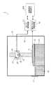
- FIG. 4 is a diagram illustrating an example of a specific configuration of the organic EL display panel inspection apparatus according to the embodiment.
- FIG. 5 is an operation flowchart for explaining the organic EL display panel inspection method according to the embodiment.
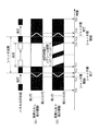
- FIG. 6 is a timing chart for explaining the organic EL display panel inspection method according to the embodiment.
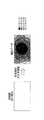
- FIG. 7A is an image diagram showing luminance values acquired by imaging a uniform light-emitting panel by the organic EL display panel inspection method according to the embodiment.
- FIG. 7A is an image diagram showing luminance values acquired by imaging a uniform light-emitting panel by the organic EL display panel inspection method according to the embodiment.
- FIG. 7B is an image diagram showing luminance values obtained by imaging a uniform light emitting panel by a conventional organic EL display panel inspection method.
- FIG. 8 is an external view of a thin flat TV manufactured using the organic EL display panel inspection method according to the embodiment.
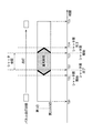
- FIG. 9 is a timing chart for explaining a display panel inspection method according to the prior art.
- the exposure period of each display pixel becomes non-uniform due to the shutter opening / closing of the CCD camera. So-called shutter unevenness is superimposed on the luminance value of each display pixel obtained from image data captured during this non-uniform exposure period.
- FIG. 9 is a timing chart for explaining a display panel inspection method according to the prior art. This figure shows the elapsed time of the lighting state of each display pixel row (1st row to 2160th row) in the display panel. In addition, the timing of opening and closing the shutter of the camera that images the display panel is shown in the same figure in relation to the lighting state of each display pixel row. Here, a mechanical shutter of a type that gradually opens outward from the center of the camera lens is illustrated. Note that the positions of the display panel and the camera are adjusted so that the center axis of the display panel and the center axis of the camera lens coincide.
- all the display pixels are uniformly lit from the inspection start time T20 to the inspection end time T25. That is, the same gradation display data is input to each display pixel.
- an operation of opening the shutter of the camera is started at time T21.
- the shutter starts to open gradually from the center of the lens.
- the operation of opening the shutter of the camera is completed.
- exposure to the display pixels disposed on the outer peripheral portion of the display panel (of the image sensor disposed on the outer peripheral portion) is started.
- the shutter is gradually opened from the lens center toward the outer periphery.
- an operation to close the shutter of the camera is started at time T23.
- the shutter starts to close from the outer periphery of the lens.
- the exposure for the display pixels arranged on the outer peripheral portion of the display panel (of the image sensor arranged on the outer peripheral portion) is completed.
- the operation of closing the camera shutter is completed.
- the exposure for the display pixel arranged at the center of the display panel (of the image sensor arranged at the center) is completed.
- the shutter is gradually closed from the outer periphery of the lens toward the center.
- the exposure period for the display pixels arranged at the center of the display panel is (T24-T21), and the exposure period for the display pixels arranged at the outer periphery of the display panel is ( T23-T22). That is, the display pixel arranged at the center of the display panel is imaged with a longer exposure period than the display pixels arranged at the outer periphery (the image sensor arranged at the center of the imaging region is The exposure period is longer than that of the image sensor arranged on the outer peripheral portion), and the exposure period varies in the display panel. Thereby, even if all the display pixels of the display panel are displayed with the same display gradation data, the variation in the exposure period is superimposed on the imaging data. For this reason, the display panel luminance value measuring method according to the prior art has a problem that display unevenness reflecting circuit element variations between display pixels cannot be accurately inspected.
- an organic EL display panel inspection method provides a display in which pixels including organic EL elements and driving elements that drive the organic EL elements are arranged in a matrix.
- An organic EL display panel inspection method for inspecting variations in brightness of a panel wherein a shutter opening step of opening a shutter of an imaging device that images the display panel in a state where all pixels of the display panel are turned off, and the shutter Are fully opened, a lighting step for lighting a plurality of target pixels for luminance measurement, a lighting-off step for turning off the plurality of target pixels after a predetermined period after the lighting step, and after the lighting-off step, A shutter closing step for closing the shutter in a state in which all pixels of the display panel are turned off, and the shutter closing step from the shutter opening step. From the image data captured by the imaging device during Tsu until flops, characterized in that it comprises a luminance calculating step of obtaining the respective luminance values of the plurality of target pixels.
- the lighting step lighting of the plurality of target pixels is started in a row sequence, and in the extinguishing step, after the period of an integral multiple of a unit frame period has elapsed after the lighting step starts,
- the target pixels may be turned off in a line-sequential manner.
- each target pixel can be set to be equal, it is possible to accurately measure the luminance value of the target pixel in the row-sequential light emitting display panel.
- the plurality of target pixels may be turned on at the same time in the lighting step, and the plurality of target pixels may be turned off at the same time in the turn-off step.
- the lighting period of each target pixel can be set to be equal, it is possible to accurately measure the luminance value of the target pixel in the simultaneous light emission type display panel.
- a panel transport step for transporting the display panel to be inspected to a dark room in which the imaging device is installed before the shutter opening step, from the shutter opening step to the shutter closing step.
- the display panel may be imaged by the imaging device in the darkroom.
- the display panel is imaged in a dark room, noise light other than the lighting light from each pixel can be suppressed. Therefore, the luminance value of each target pixel can be measured more accurately.
- the present invention can be realized not only as an organic EL display panel inspection method including such characteristic steps, but also as an organic EL display panel inspection apparatus that realizes characteristic steps included in the inspection method. Produces the same effect as described above.
- An organic EL display panel inspection apparatus is an organic EL display that inspects luminance variations of a display panel in which pixels including organic EL elements and drive elements that drive the organic EL elements are arranged in a matrix.
- a panel inspection apparatus having a shutter for determining whether to capture or block incident light, and an image pickup apparatus for picking up an image of the display panel, and an opening / closing operation of the shutter in a state in which all pixels of the display panel are turned off. After the shutter is fully opened, a plurality of target pixels whose luminance is to be measured are turned on, and after a predetermined period, the plurality of target pixels are turned off, and the shutter is opened.
- a calculation unit that obtains luminance values of each of the plurality of target pixels from imaging data captured by the imaging apparatus during a period until a closing operation;
- the display panel control unit turns on the plurality of target pixels after the shutter is fully opened, and completes the turn-off of the plurality of target pixels before starting the shutter closing operation.
- the luminance value of the target pixel can be accurately measured without being affected by variations in the exposure period.
- the shutter may be a mechanical shutter that gradually opens from the center of the imaging lens of the imaging device toward the outer periphery and gradually closes from the outer periphery of the imaging lens toward the center.
- the imaging device has a configuration in which the imaging lens is opened and closed with a mechanical shutter, the luminance value of the target pixel is accurately measured without being affected by variations in the exposure period associated with opening and closing the shutter of the imaging device. It becomes possible to do.
- a dark room storing the imaging device and the display panel to be inspected
- a transport mechanism for transporting the display panel to be inspected to a predetermined position in the dark room, the imaging device and the inspection target
- an adjustment mechanism for adjusting the positional relationship with the display panel.
- the display panel is imaged in a dark room, noise light other than the lighting light from each pixel can be suppressed. Furthermore, it is possible to measure the luminance value of the target pixel more accurately by a mechanism that can adjust the positional relationship between the imaging device and the display panel.
- the organic EL display panel inspection apparatus of the present invention is a concept including system equipment such as information equipment.
- FIG. 1 is a block diagram showing a configuration of an inspection system including an organic EL display panel inspection apparatus according to an embodiment.
- the inspection system in FIG. 1 includes a display panel 4 to be inspected and an organic EL display panel inspection apparatus 1.
- the organic EL display panel inspection apparatus 1 is an apparatus that inspects luminance variations (display unevenness) of pixels arranged in a matrix on the display panel 4, and includes a control unit 10, a camera 20, and a storage unit 30.
- the control unit 10 includes a camera control circuit 11, a display panel control circuit 12, and a calculation unit 13.
- the camera 20 is, for example, a CCD (Charge Coupled Device) camera, and is an imaging device that images the display panel 4.
- the camera 20 includes an imaging region in which a plurality of imaging elements arranged in a matrix is arranged, an imaging lens that collects incident light on the plurality of imaging elements, and light collection and shielding of incident light to the imaging lens. And a shutter for determining.
- the camera 20 makes light emitted from pixels arranged in a matrix on the display panel 4 enter the imaging region via the imaging lens.
- Each of the plurality of imaging elements converts incident light into a charge amount corresponding to the amount of incident light.
- the positions of the display panel 4 and the camera 20 are adjusted so that the central axis of the display panel 4 and the central axis of the imaging lens coincide.
- the image sensor arranged in the central part of the imaging region receives the emitted light from the pixels arranged in the central part of the display panel 4 and generates a charge amount corresponding to the emitted light.
- the image sensor arranged at the outer peripheral part of the imaging region receives the emitted light from the pixels arranged at the outer peripheral part of the display panel 4 and generates a charge amount corresponding to the emitted light.
- the camera control circuit 11 is a camera control unit that opens and closes the shutter of the camera 20 in a state where all the pixels of the display panel 4 are turned off.
- the display panel control circuit 12 After the shutter of the camera 20 is fully opened, the display panel control circuit 12 starts to turn on a plurality of target pixels whose luminance is to be measured on the display panel 4, and starts turning off the plurality of target pixels after a predetermined exposure period has elapsed.
- a display panel control unit After the shutter of the camera 20 is fully opened, the display panel control circuit 12 starts to turn on a plurality of target pixels whose luminance is to be measured on the display panel 4, and starts turning off the plurality of target pixels after a predetermined exposure period has elapsed.
- the calculation unit 13 obtains the luminance values of the plurality of target pixels from the image data captured by the camera 20. Specifically, the calculation unit 13 obtains the luminance value of the pixel arranged in the central part of the display panel 4 based on the imaging data of the imaging element arranged in the central part of the imaging area of the camera 20, and the imaging area of the camera 20. The luminance value of the pixel arranged in the outer peripheral part of the display panel 4 is obtained from the imaging data of the image sensor arranged in the outer peripheral part.
- the storage unit 30 is a memory that stores the luminance data of the target pixel obtained by the calculation unit 13.
- the storage unit 30 may be a memory built in the control unit 10.
- FIG. 2 is a block diagram showing the configuration of the display panel.
- the display panel 4 includes a display unit 41, a scanning line driving circuit 42, and a data line driving circuit 43.
- the display unit 41 is a display area in which pixels including organic EL elements and drive elements that drive the organic EL elements are arranged in a matrix.
- the scanning line driving circuit 42 selects a pixel row to which a data voltage corresponding to the gradation data is written through the scanning line arranged for each pixel row.
- the data line driving circuit 43 outputs a data voltage to the pixels belonging to the selected pixel row via the data line arranged for each pixel column.
- FIG. 3 is a diagram illustrating an example of a circuit configuration of a pixel and connection with peripheral circuits.
- a pixel 400 in the drawing includes a scanning line 410, a data line 420, a power supply line 430, a selection transistor 401, a driving transistor 402, an organic EL element 403, a storage capacitor element 404, and a common electrode 405.
- the peripheral circuit includes a scanning line driving circuit 42 and a data line driving circuit 43.
- the scanning line driving circuit 42 is connected to the scanning line 410 and has a function of controlling conduction and non-conduction of the selection transistor 401 of the pixel 400.
- the data line driving circuit 43 is connected to the data line 420 and has a function of outputting a data voltage and determining a signal current flowing through the driving transistor 402.
- the selection transistor 401 has a gate connected to the scanning line 410 and has a function of controlling the timing at which the data voltage of the data line 420 is supplied to the gate of the driving transistor 402.
- the drive transistor 402 functions as a drive element, the gate of the drive transistor 402 is connected to the data line 420 via the selection transistor 401, the source is connected to the anode of the organic EL element 403, and the drain is connected to the power supply line 430. ing. Accordingly, the drive transistor 402 converts the data voltage supplied to the gate into a signal current corresponding to the data voltage, and supplies the converted signal current to the organic EL element 403.
- the organic EL element 403 functions as a light emitting element, and the cathode of the organic EL element 403 is connected to the common electrode 405.
- the storage capacitor element 404 is connected between the power supply line 430 and the gate terminal of the drive transistor 402.
- the storage capacitor element 404 has a function of maintaining the immediately preceding gate voltage and continuously supplying a drive current from the drive transistor 402 to the organic EL element 403 even after the selection transistor 401 is turned off.
- the power line 430 is connected to a power source.
- the common electrode 405 is also connected to another power source.
- the data voltage supplied from the data line driving circuit 43 is applied to the gate terminal of the driving transistor 402 via the selection transistor 401.
- the drive transistor 402 passes a current corresponding to the data voltage between the source and drain terminals. When this current flows to the organic EL element 403, the organic EL element 403 emits light with light emission luminance corresponding to the current.
- FIG. 4 is a diagram showing an example of a specific configuration of the organic EL display panel inspection apparatus according to the embodiment.
- the organic EL display panel inspection apparatus 1 shown in FIG. 1 includes a control signal generating PC 10A, a camera control circuit 11, a display panel control circuit 12, a dark room 19, a position adjustment table 14, a transfer table 15, and a transfer.
- a table moving device 16, a camera 20, a column 23, and a camera fixing table 24 are provided.
- the control signal generating PC 10A is a control unit including a calculation unit 13 and a storage unit 30, and for example, a personal computer is applied.
- the control signal generating PC 10A instructs the camera control circuit 11 when to open and close the shutter of the camera 20 with all the pixels of the display panel 4 turned off. Further, the control signal generating PC 10A causes the display panel control circuit 12 to start lighting the target pixel for measuring the luminance of the display panel 4 after the shutter of the camera 20 is fully opened, and after the elapse of a predetermined exposure period, The timing to start turning off the target pixel is instructed. Further, the control signal generating PC 10A obtains the luminance value of each of the plurality of target pixels whose luminance is to be measured from the imaging data captured by the camera 20, and stores the luminance value.
- the camera control circuit 11 outputs to the camera 20 an opening / closing signal for opening / closing the shutter of the camera 20 in a state where all the pixels of the display panel 4 are turned off in accordance with an instruction from the control signal generating PC 10A.
- the display panel control circuit 12 follows a command from the control signal generating PC 10A, and after the shutter of the camera 20 is fully opened, a lighting signal for starting lighting of a target pixel whose luminance is to be measured on the display panel 4, and a predetermined exposure period. After the elapse of time, a turn-off signal for starting turn-off of the target pixel is output to the scanning line drive circuit 42 and the data line drive circuit 43.
- the display panel control circuit 12 may be a control circuit built in a display device in which the display panel 4 to be inspected is incorporated.
- the control circuit of the display device controls the scanning line driving circuit 42 and the data line driving circuit 43 in accordance with an instruction from the control signal generating PC 10A at the time of manufacture.
- the control circuit of the display device stores, for example, correction parameters for correcting the data voltage from the luminance data acquired by the organic EL display panel inspection device 1 in the memory when the manufacture is completed.
- the control circuit of the display device reads the correction parameter, corrects the video signal data input from the outside based on the correction parameter, and outputs the video signal data to the data line driving circuit 43.
- the camera 20 is a CCD camera and has a lens 21 and a shutter 22.
- the lens 21 condenses incident light on each image sensor of the camera 20.
- the shutter 22 is a mechanical shutter that gradually opens from the central portion of the lens 21 toward the outer peripheral portion and closes gradually from the outer peripheral portion of the lens 21 toward the central portion. Note that the shutter 22 does not have to gradually open and close between the lens center portion and the outer peripheral portion as described above, as long as it requires a predetermined time from opening to closing of the shutter and from opening to closing of the shutter.
- a type sliding door type that gradually opens and closes from one end on the outer periphery of the lens 21 toward the other end facing the one end.
- the dark room 19 stores the camera 20 and the display panel 4 to be inspected. Thereby, noise light other than the lighting light from each pixel can be suppressed, and the luminance value of the target pixel can be measured more accurately.
- the darkroom 19 is provided with a confirmation window 18 and a display panel carry-in port 17. It becomes possible to confirm the position and lighting state of the display panel 4 installed in the dark room 19 by the confirmation window 18.
- the display panel 4 to be inspected is sequentially carried into the dark room 19 via the display panel carry-in port 17.
- the position adjusting table 14 is installed inside the dark room 19, and the display panel 4 to be inspected is disposed together with the transport table 15 thereon.
- the position adjustment table 14 has an adjustment mechanism that can adjust the horizontal position (XYZ) and rotation ( ⁇ ).
- the transport table 15 is a carrier on which the display panel 4 is placed and the display panel 4 to be inspected is arranged at a predetermined position in the dark room 19.
- the transport table moving device 16 is a transport mechanism that guides the pair of transport tables 15 and the display panel 4 carried in from the display panel carry-in port 17 to the position adjustment table 14.
- the organic EL display panel inspection apparatus 1 can be incorporated in the middle of the display panel mass production process.
- the column 23 has an adjustment mechanism that can move the camera fixing base 24 up and down and rotate in the horizontal direction while fixing the camera fixing base 24 to which the camera is fixed.
- the camera fixing base 24 has a tilt mechanism capable of rotating the camera 20 on the fixed surface while fixing the camera 20.
- the positional relationship between the camera 20 and the display panel 4 can be adjusted by the adjusting mechanism of the position adjusting table 14 and the column 23 and the tilt mechanism of the camera fixing table 24.
- the central axis of the lens 21 and the central axis of the display unit 41 can be matched. As a result, the luminance value of the target pixel can be measured more accurately.
- FIG. 5 is an operation flowchart for explaining the organic EL display panel inspection method according to the embodiment.
- FIG. 6 is a timing chart for explaining the organic EL display panel inspection method according to the embodiment.
- FIG. 6 shows the elapsed time of the lighting state of each pixel row (first row to second 1602 row) in the display panel 4.
- FIG. 6A shows a lighting state in a display driving method without a black insertion period
- FIG. 6B shows a display driving method with a black insertion period.
- the lighting state at is shown.
- the display method shown in FIG. 6A is a display method in which all the pixels are turned on and off simultaneously
- the display method shown in FIG. This is a display method in which the light is turned on and the line is sequentially turned off.
- FIG. 6 shows the shutter opening / closing timing of the camera 20 that images the display panel 4 in association with the lighting state of each pixel row.
- the shutter 22 of the camera 20 is an example of a mechanical shutter that gradually opens from the center of
- the display panel 4 to be inspected is carried into the dark room 19.
- the position of the display panel 4 and the camera 20 is adjusted by the mechanism of the position adjustment base 14, the column 23, and the camera fixing base 24 so that the central axis of the display unit 41 and the central axis of the lens 21 coincide.
- the position adjustment table 14, the transfer table 15, the transfer table moving device 16, the support column 23, and the camera fixing table 24 may be excluded depending on the required accuracy of the luminance value.
- the camera control circuit 11 starts an operation of opening the shutter 22 with respect to the camera 20 with all the pixels of the display panel 4 turned off (S10: shutter opening step).
- the shutter 22 starts to gradually open from the center of the lens 21.
- exposure is performed with black gradation.
- the operation of opening the shutter 22 is completed.
- the shutter 22 gradually opens from the center of the lens 21 toward the outer periphery.
- the period from time T11 to T12, that is, the shutter opening operation time is, for example, 50 msec.
- the display panel control circuit 12 starts lighting each pixel of the display panel 4 in a state where the opening operation of the shutter 22 is completed (fully opened) (S20: lighting step).
- S20 lighting step
- all the pixels of the display panel 4 are turned on simultaneously at time T13.
- the display drive method with black insertion FIG. 6B
- row sequential lighting is started for each pixel of the display panel 4 at time T13.
- the period from time T12 to T13 that is, the time from the completion of the shutter opening operation to the start of lighting is preferably, for example, 250 msec (about 30 frame periods: frequency 120 Hz, one frame period 8.3 msec) or more. .
- This time corresponds to the opening operation time of the shutter 22 being 50 msec, and also takes into account the period until the shutter vibration and other unstable factors are stabilized immediately after the shutter 22 is fully opened. is there.
- the display panel control circuit 12 lights each pixel in a period that is an integral multiple of the unit frame period (S30).
- the lighting time of each pixel is the same because all the pixels are simultaneously turned on and off during the lighting period from time T13 to time T14.
- the display driving method with black insertion ((b) in FIG. 6)
- the case where each pixel is lit for two frame periods in the lighting period from time T13 to time T14 is illustrated.
- a black insertion period is provided sequentially.
- the period from time T13 to T14, that is, the lighting period of each pixel is preferably set to, for example, 25 msec (about 3 frame periods: frequency 120 Hz, 1 frame period 8.3 msec) or more.
- the display panel control circuit 12 starts turning off each pixel of the display panel 4 after an integral multiple of the unit frame period has elapsed (S40: turn-off step).
- S40 turn-off step
- all the pixels of the display panel 4 are turned off simultaneously at time T14.
- the display driving method with black insertion ((b) of FIG. 6)
- the row sequential turn-off of each pixel of the display panel 4 is started at time T14.
- the camera control circuit 11 starts the operation of closing the shutter 22 with respect to the camera 20 with all the pixels of the display panel 4 turned off (S50: shutter closing step). At this time, the shutter 22 starts to close gradually from the outer periphery of the lens 21.
- the calculation unit 13 obtains each luminance value of the target pixel from the image data captured by the camera 20 from the shutter opening step to the shutter closing step (luminance calculation step).
- the control unit 10 causes the camera 20 to image the display panel 4 from the shutter opening step (S10) to the shutter closing step (S50).
- the camera 20 substantially images the display panel 4 during the period from the lighting step (S20) to the extinguishing step (S40).
- the period during which each pixel of the display panel 4 is lit is not affected by the opening / closing of the shutter 22.
- the lighting period of each pixel is The same regardless of the pixel row. That is, it is possible to accurately measure the luminance value of the target pixel without being affected by variations in the exposure period associated with the opening / closing of the shutter of the camera 20. Therefore, it is possible to accurately inspect the luminance variation (display unevenness) of the display panel 4.
- FIG. 7A is an image diagram showing a luminance value acquired by imaging a uniform light-emitting panel by the organic EL display panel inspection method according to the embodiment.
- FIG. 7B is an image diagram showing luminance values acquired by imaging a uniform light-emitting panel by a display panel inspection method according to the prior art.
- the lighting state of the display unit in which all pixels emit light uniformly is shown on the left side.
- FIGS. 7A and 7B on the right side, there are shown image diagrams of imaging data acquired by the organic EL display panel inspection method according to the present embodiment and the display panel inspection method according to the conventional technique, respectively.
- a luminance variation of up to 4% (1.00 to 0.96 in the figure) is observed with respect to the display gradation width (1.00 in the figure), and from the central part to the outer peripheral part.
- the distribution has a decreasing brightness. This is because the operation of the mechanical shutter causes the pixels arranged in the central portion of the display panel 4 to be imaged with a longer exposure period than the pixels arranged in the outer peripheral portion. This is considered to be caused by the occurrence of variations in the above. Thereby, even if all the display pixels of the display panel 4 are displayed by the same display gradation data, the variation of the exposure period is superimposed on the imaging data. For this reason, the luminance value measurement method for the display panel 4 according to the conventional technique cannot accurately measure luminance variations reflecting circuit element variations between display pixels.
- the luminance fluctuation is within 1% (1.00 to 0.99 in the figure) with respect to the display gradation width (1.00 in the figure). This is considered to be caused by the camera 20 being able to image the display panel 4 without being affected by variations in the exposure period accompanying the opening and closing of the shutter of the camera 20. Therefore, the luminance values of all the pixels can be accurately measured, and the luminance variation of the display panel 4 can be accurately inspected.
- the organic EL display panel inspection method and the organic EL display panel inspection apparatus according to the present embodiment are not limited to the above embodiment. Modifications obtained by making various modifications conceivable by those skilled in the art without departing from the gist of the present invention with respect to the above-described embodiment, and various apparatuses incorporating the organic EL display panel inspection apparatus according to this embodiment It is included in the present invention.
- the organic EL display panel inspection apparatus is included in an apparatus for manufacturing a thin flat TV display panel as shown in FIG.
- the organic EL display panel inspection apparatus and the organic EL display panel inspection method according to the present embodiment a low-cost thin flat TV having a long-life display in which display unevenness is suppressed is realized.
- the organic EL display panel inspection apparatus and the organic EL display panel inspection method according to the above-described embodiment As described above, even when the pixel on / off direction and the mechanical shutter opening / closing direction coincide with each other, by using the organic EL display panel inspection apparatus and the organic EL display panel inspection method according to the above-described embodiment, The luminance value of the target pixel can be accurately measured without synchronizing the on / off line speed and the shutter opening / closing speed. Therefore, it is possible to accurately inspect the luminance variation (display unevenness) of the display panel.
- the present invention includes a case where, among all the pixels of the display unit 41, only a plurality of target pixels whose luminance is to be measured are turned on and off, and luminance variations of the plurality of target pixels are measured. For example, when inspecting display unevenness for each display area by dividing the display unit into a plurality of display areas, a representative pixel is specified for each display area, and luminance variation is measured using the representative pixel as the plurality of target pixels. Also good. By evaluating the luminance variation of the representative pixels, it is possible to inspect display unevenness for each display region.
- the present invention is particularly useful for an organic EL flat panel display incorporating an organic EL display device, and is optimal for use as a display inspection apparatus and inspection method that require uniformity in image quality.
Landscapes
- Engineering & Computer Science (AREA)
- Physics & Mathematics (AREA)
- Computer Hardware Design (AREA)
- General Physics & Mathematics (AREA)
- Theoretical Computer Science (AREA)
- Electroluminescent Light Sources (AREA)
Abstract
L'invention concerne un procédé d'inspection d'un panneau d'affichage électroluminescent organique destiné à inspecter les variations de luminance d'un panneau d'affichage dans lequel des pixels sont disposés en matrices, chacun desdits pixels incluant un élément électroluminescent organique et un élément de pilotage. Le procédé comprend : une étape (S10) d'ouverture d'un obturateur d'un appareil photo dans un état dans lequel tous les pixels du panneau d'affichage sont désactivés; une étape (S20) d'activation de tous les pixels après l'ouverture complète de l'obturateur; une étape (S40) de désactivation de tous les pixels après écoulement d'une durée prédéterminée après l'étape (S20); une étape (S50) de fermeture de l'obturateur, après l'étape (S40), dans un état dans lequel tous les pixels du panneau d'affichage sont désactivés; et une étape d'obtention d'une valeur de luminance de chacun de la totalité des pixels en se basant sur les données des images capturées au moyen de l'appareil photo pendant une période durant de l'étape (S10) à l'étape (S50).
Applications Claiming Priority (2)
| Application Number | Priority Date | Filing Date | Title |
|---|---|---|---|
| JP2014-013811 | 2014-01-28 | ||
| JP2014013811 | 2014-01-28 |
Publications (1)
| Publication Number | Publication Date |
|---|---|
| WO2015114720A1 true WO2015114720A1 (fr) | 2015-08-06 |
Family
ID=53756342
Family Applications (1)
| Application Number | Title | Priority Date | Filing Date |
|---|---|---|---|
| PCT/JP2014/006351 Ceased WO2015114720A1 (fr) | 2014-01-28 | 2014-12-19 | Procédé d'inspection d'un panneau d'affichage électroluminescent organique et appareil d'inspection d'un panneau d'affichage électroluminescent organique |
Country Status (1)
| Country | Link |
|---|---|
| WO (1) | WO2015114720A1 (fr) |
Cited By (15)
| Publication number | Priority date | Publication date | Assignee | Title |
|---|---|---|---|---|
| US12080224B2 (en) | 2022-12-19 | 2024-09-03 | Stereyo Bv | Configurations, methods, and devices for improved visual performance of a light-emitting element display and/or a camera recording an image from the display |
| US12100363B2 (en) | 2022-12-19 | 2024-09-24 | Stereyo Bv | Configurations, methods, and devices for improved visual performance of a light-emitting element display and/or a camera recording an image from the display |
| US12112695B2 (en) | 2022-12-19 | 2024-10-08 | Stereyo Bv | Display systems and methods with multiple and/or adaptive primary colors |
| US12119330B2 (en) | 2022-12-19 | 2024-10-15 | Stereyo Bv | Configurations, methods, and devices for improved visual performance of a light-emitting element display and/or a camera recording an image from the display |
| EP4390916A3 (fr) * | 2022-12-19 | 2024-10-16 | Stereyo BV | Dispositif d'affichage à matrice active, système et procédé |
| US12185585B2 (en) | 2022-12-19 | 2024-12-31 | Stereyo Bv | Active matrix display, system, and method having an additional transistor that discharges a storage capacitor within pixel circuits, at least one pixel circuit driven by a drive circuit resides physical within another drive circuit, and/or off-to-on time of scan signals are set in relation to an operation of a camera recording the display |
| US12199079B2 (en) | 2022-12-19 | 2025-01-14 | Stereyo Bv | Configurations, methods, and devices for improved visual performance of a light-emitting element display and/or a camera recording an image from the display |
| CN119413413A (zh) * | 2025-01-06 | 2025-02-11 | 浙江老鹰半导体技术有限公司 | 激光芯片的近场图像数据获取系统、方法及计算机设备、存储介质、程序产品 |
| US12425538B2 (en) | 2022-07-15 | 2025-09-23 | Stereyo Bv | Focused sound and infotainment system and method |
| US12443384B2 (en) | 2022-12-19 | 2025-10-14 | Stereyo Bv | Display system and method for mapping of images |
| US12455056B2 (en) | 2022-08-08 | 2025-10-28 | Stereyo Bv | Photovoltaic sunshade and display system |
| US12494165B2 (en) | 2019-03-07 | 2025-12-09 | Stereyo Bv | Real-time deformable and transparent display |
| US12499820B2 (en) | 2022-12-19 | 2025-12-16 | Stereyo Bv | Systems and methods for altering light output and white point of a light source or light source display |
| US12506923B2 (en) | 2022-12-19 | 2025-12-23 | Stereyo Bv | Video processing in modular display system and method |
| US12505785B2 (en) | 2019-06-07 | 2025-12-23 | Stereyo Bv | Systems, methods, and devices for improved light-emitting display and interplay |
Citations (5)
| Publication number | Priority date | Publication date | Assignee | Title |
|---|---|---|---|---|
| JP2010151666A (ja) * | 2008-12-25 | 2010-07-08 | Toray Ind Inc | パターン検査装置および検査方法 |
| JP2010266502A (ja) * | 2009-05-12 | 2010-11-25 | Casio Computer Co Ltd | 表示装置の製造装置及び表示装置の製造方法 |
| JP2011038938A (ja) * | 2009-08-13 | 2011-02-24 | Fujitsu Ltd | 表示装置の検査方法及び検査装置 |
| JP2011049159A (ja) * | 2009-07-28 | 2011-03-10 | Semiconductor Energy Lab Co Ltd | 発光装置の検査方法及び作製方法 |
| JP2013079880A (ja) * | 2011-10-04 | 2013-05-02 | Fujitsu Ltd | 画質検査方法、画質検査装置及び画質検査プログラム |
-
2014
- 2014-12-19 WO PCT/JP2014/006351 patent/WO2015114720A1/fr not_active Ceased
Patent Citations (5)
| Publication number | Priority date | Publication date | Assignee | Title |
|---|---|---|---|---|
| JP2010151666A (ja) * | 2008-12-25 | 2010-07-08 | Toray Ind Inc | パターン検査装置および検査方法 |
| JP2010266502A (ja) * | 2009-05-12 | 2010-11-25 | Casio Computer Co Ltd | 表示装置の製造装置及び表示装置の製造方法 |
| JP2011049159A (ja) * | 2009-07-28 | 2011-03-10 | Semiconductor Energy Lab Co Ltd | 発光装置の検査方法及び作製方法 |
| JP2011038938A (ja) * | 2009-08-13 | 2011-02-24 | Fujitsu Ltd | 表示装置の検査方法及び検査装置 |
| JP2013079880A (ja) * | 2011-10-04 | 2013-05-02 | Fujitsu Ltd | 画質検査方法、画質検査装置及び画質検査プログラム |
Cited By (16)
| Publication number | Priority date | Publication date | Assignee | Title |
|---|---|---|---|---|
| US12494165B2 (en) | 2019-03-07 | 2025-12-09 | Stereyo Bv | Real-time deformable and transparent display |
| US12505785B2 (en) | 2019-06-07 | 2025-12-23 | Stereyo Bv | Systems, methods, and devices for improved light-emitting display and interplay |
| US12425538B2 (en) | 2022-07-15 | 2025-09-23 | Stereyo Bv | Focused sound and infotainment system and method |
| US12455056B2 (en) | 2022-08-08 | 2025-10-28 | Stereyo Bv | Photovoltaic sunshade and display system |
| EP4390916A3 (fr) * | 2022-12-19 | 2024-10-16 | Stereyo BV | Dispositif d'affichage à matrice active, système et procédé |
| US12185585B2 (en) | 2022-12-19 | 2024-12-31 | Stereyo Bv | Active matrix display, system, and method having an additional transistor that discharges a storage capacitor within pixel circuits, at least one pixel circuit driven by a drive circuit resides physical within another drive circuit, and/or off-to-on time of scan signals are set in relation to an operation of a camera recording the display |
| US12199079B2 (en) | 2022-12-19 | 2025-01-14 | Stereyo Bv | Configurations, methods, and devices for improved visual performance of a light-emitting element display and/or a camera recording an image from the display |
| US12080224B2 (en) | 2022-12-19 | 2024-09-03 | Stereyo Bv | Configurations, methods, and devices for improved visual performance of a light-emitting element display and/or a camera recording an image from the display |
| US12443384B2 (en) | 2022-12-19 | 2025-10-14 | Stereyo Bv | Display system and method for mapping of images |
| US12119330B2 (en) | 2022-12-19 | 2024-10-15 | Stereyo Bv | Configurations, methods, and devices for improved visual performance of a light-emitting element display and/or a camera recording an image from the display |
| US12112695B2 (en) | 2022-12-19 | 2024-10-08 | Stereyo Bv | Display systems and methods with multiple and/or adaptive primary colors |
| US12499820B2 (en) | 2022-12-19 | 2025-12-16 | Stereyo Bv | Systems and methods for altering light output and white point of a light source or light source display |
| US12506923B2 (en) | 2022-12-19 | 2025-12-23 | Stereyo Bv | Video processing in modular display system and method |
| US12100363B2 (en) | 2022-12-19 | 2024-09-24 | Stereyo Bv | Configurations, methods, and devices for improved visual performance of a light-emitting element display and/or a camera recording an image from the display |
| CN119413413A (zh) * | 2025-01-06 | 2025-02-11 | 浙江老鹰半导体技术有限公司 | 激光芯片的近场图像数据获取系统、方法及计算机设备、存储介质、程序产品 |
| CN119413413B (zh) * | 2025-01-06 | 2025-05-02 | 浙江老鹰半导体技术有限公司 | 激光芯片的近场图像数据获取系统、方法及计算机设备、存储介质、程序产品 |
Similar Documents
| Publication | Publication Date | Title |
|---|---|---|
| WO2015114720A1 (fr) | Procédé d'inspection d'un panneau d'affichage électroluminescent organique et appareil d'inspection d'un panneau d'affichage électroluminescent organique | |
| JP5010814B2 (ja) | 有機el表示装置の製造方法 | |
| US10269275B2 (en) | Display panel inspecting method and display panel fabricating method | |
| JP4844602B2 (ja) | 表示装置、表示制御装置、および表示制御方法、並びにプログラム | |
| KR100951461B1 (ko) | 기판 에지 검사장치 및 방법 | |
| WO2009144936A1 (fr) | Dispositif d’affichage, et procédé de fabrication et procédé de commande de ce dispositif | |
| CN117116207B (zh) | 一种灰阶补偿方法及系统 | |
| CN113744704B (zh) | 显示面板的亮度调节方法及装置 | |
| JP5995165B2 (ja) | 表示装置の検査方法、検査装置及び製造方法 | |
| JP4880536B2 (ja) | 透過型表示パネルの検査装置、透過型表示パネルの検査方法、透過型表示パネルの製造方法、プログラム及び記録媒体 | |
| WO2020136730A1 (fr) | Système de génération d'image de correction, programme de commande d'image et support d'enregistrement | |
| WO2013115356A1 (fr) | Dispositif d'affichage d'image, appareil électronique, caméra électronique, et terminal d'informations | |
| KR20100035384A (ko) | 디지털 영상 신호 처리 장치의 제어 방법 및 상기 제어 방법에 따라 동작하는 디지털 영상 신호 처리 장치 | |
| JP2011027907A (ja) | 輝度ムラ修正用補正データの作成方法及びその作成装置 | |
| JP2015222332A (ja) | 表示パネルの製造方法 | |
| JP6722366B1 (ja) | 補正画像生成システム、画像制御方法、画像制御プログラム、および記録媒体 | |
| KR20210011542A (ko) | 테스트 영상 측정 장치, 표시 장치 및 휘도 보정 방법 | |
| JP6312103B2 (ja) | 表示パネルの寿命特性の検査方法及び表示パネルの製造方法 | |
| JP2008076611A (ja) | プロジェクタ、画像表示装置および液晶照射方法 | |
| US12488492B2 (en) | Method of obtaining brightness information of display panel and related panel detection system | |
| KR20160079246A (ko) | 얼룩 보상 장치 및 그를 가지는 평판 표시 장치의 화질 보상 장치 | |
| WO2020136732A1 (fr) | Système de génération d'image de correction, procédé de commande d'image, programme de commande d'image et support d'enregistrement | |
| JP2020112812A (ja) | 補正画像生成システム、画像制御プログラム、および記録媒体 | |
| JP5310811B2 (ja) | 温度ムラ補正量決定方法、表示装置、温度ムラ補正量決定装置、温度ムラ補正装置及びプログラム | |
| JP2008102818A (ja) | 撮像手段の出力値補正方法、シェーディング補正方法、欠陥検出方法、欠陥検出プログラムおよび欠陥検出装置 |
Legal Events
| Date | Code | Title | Description |
|---|---|---|---|
| 121 | Ep: the epo has been informed by wipo that ep was designated in this application |
Ref document number: 14880776 Country of ref document: EP Kind code of ref document: A1 |
|
| NENP | Non-entry into the national phase |
Ref country code: DE |
|
| 122 | Ep: pct application non-entry in european phase |
Ref document number: 14880776 Country of ref document: EP Kind code of ref document: A1 |
|
| NENP | Non-entry into the national phase |
Ref country code: JP |