WO2015115236A1 - 脈波検出装置 - Google Patents
脈波検出装置 Download PDFInfo
- Publication number
- WO2015115236A1 WO2015115236A1 PCT/JP2015/051273 JP2015051273W WO2015115236A1 WO 2015115236 A1 WO2015115236 A1 WO 2015115236A1 JP 2015051273 W JP2015051273 W JP 2015051273W WO 2015115236 A1 WO2015115236 A1 WO 2015115236A1
- Authority
- WO
- WIPO (PCT)
- Prior art keywords
- pressure sensor
- pulse wave
- array
- pressure
- detection device
- Prior art date
- Legal status (The legal status is an assumption and is not a legal conclusion. Google has not performed a legal analysis and makes no representation as to the accuracy of the status listed.)
- Ceased
Links
- 0 CCC1C#CC(C)*1 Chemical compound CCC1C#CC(C)*1 0.000 description 1
Images




Classifications
-
- A—HUMAN NECESSITIES
- A61—MEDICAL OR VETERINARY SCIENCE; HYGIENE
- A61B—DIAGNOSIS; SURGERY; IDENTIFICATION
- A61B5/00—Measuring for diagnostic purposes; Identification of persons
- A61B5/02—Detecting, measuring or recording for evaluating the cardiovascular system, e.g. pulse, heart rate, blood pressure or blood flow
- A61B5/024—Measuring pulse rate or heart rate
- A61B5/0245—Measuring pulse rate or heart rate by using sensing means generating electric signals, i.e. ECG signals
-
- A—HUMAN NECESSITIES
- A61—MEDICAL OR VETERINARY SCIENCE; HYGIENE
- A61B—DIAGNOSIS; SURGERY; IDENTIFICATION
- A61B5/00—Measuring for diagnostic purposes; Identification of persons
- A61B5/02—Detecting, measuring or recording for evaluating the cardiovascular system, e.g. pulse, heart rate, blood pressure or blood flow
- A61B5/021—Measuring pressure in heart or blood vessels
- A61B5/02108—Measuring pressure in heart or blood vessels from analysis of pulse wave characteristics
-
- A—HUMAN NECESSITIES
- A61—MEDICAL OR VETERINARY SCIENCE; HYGIENE
- A61B—DIAGNOSIS; SURGERY; IDENTIFICATION
- A61B5/00—Measuring for diagnostic purposes; Identification of persons
- A61B5/02—Detecting, measuring or recording for evaluating the cardiovascular system, e.g. pulse, heart rate, blood pressure or blood flow
- A61B5/024—Measuring pulse rate or heart rate
- A61B5/02444—Details of sensor
-
- A—HUMAN NECESSITIES
- A61—MEDICAL OR VETERINARY SCIENCE; HYGIENE
- A61B—DIAGNOSIS; SURGERY; IDENTIFICATION
- A61B5/00—Measuring for diagnostic purposes; Identification of persons
- A61B5/72—Signal processing specially adapted for physiological signals or for diagnostic purposes
- A61B5/7225—Details of analogue processing, e.g. isolation amplifier, gain or sensitivity adjustment, filtering, baseline or drift compensation
-
- A—HUMAN NECESSITIES
- A61—MEDICAL OR VETERINARY SCIENCE; HYGIENE
- A61B—DIAGNOSIS; SURGERY; IDENTIFICATION
- A61B5/00—Measuring for diagnostic purposes; Identification of persons
- A61B5/72—Signal processing specially adapted for physiological signals or for diagnostic purposes
- A61B5/7235—Details of waveform analysis
-
- A—HUMAN NECESSITIES
- A61—MEDICAL OR VETERINARY SCIENCE; HYGIENE
- A61B—DIAGNOSIS; SURGERY; IDENTIFICATION
- A61B5/00—Measuring for diagnostic purposes; Identification of persons
- A61B5/72—Signal processing specially adapted for physiological signals or for diagnostic purposes
- A61B5/7235—Details of waveform analysis
- A61B5/725—Details of waveform analysis using specific filters therefor, e.g. Kalman or adaptive filters
-
- A—HUMAN NECESSITIES
- A61—MEDICAL OR VETERINARY SCIENCE; HYGIENE
- A61B—DIAGNOSIS; SURGERY; IDENTIFICATION
- A61B5/00—Measuring for diagnostic purposes; Identification of persons
- A61B5/74—Details of notification to user or communication with user or patient; User input means
- A61B5/742—Details of notification to user or communication with user or patient; User input means using visual displays
-
- A—HUMAN NECESSITIES
- A61—MEDICAL OR VETERINARY SCIENCE; HYGIENE
- A61B—DIAGNOSIS; SURGERY; IDENTIFICATION
- A61B2562/00—Details of sensors; Constructional details of sensor housings or probes; Accessories for sensors
- A61B2562/02—Details of sensors specially adapted for in-vivo measurements
- A61B2562/0247—Pressure sensors
-
- A—HUMAN NECESSITIES
- A61—MEDICAL OR VETERINARY SCIENCE; HYGIENE
- A61B—DIAGNOSIS; SURGERY; IDENTIFICATION
- A61B2562/00—Details of sensors; Constructional details of sensor housings or probes; Accessories for sensors
- A61B2562/02—Details of sensors specially adapted for in-vivo measurements
- A61B2562/028—Microscale sensors, e.g. electromechanical sensors [MEMS]
-
- A—HUMAN NECESSITIES
- A61—MEDICAL OR VETERINARY SCIENCE; HYGIENE
- A61B—DIAGNOSIS; SURGERY; IDENTIFICATION
- A61B2562/00—Details of sensors; Constructional details of sensor housings or probes; Accessories for sensors
- A61B2562/04—Arrangements of multiple sensors of the same type
- A61B2562/043—Arrangements of multiple sensors of the same type in a linear array
-
- A—HUMAN NECESSITIES
- A61—MEDICAL OR VETERINARY SCIENCE; HYGIENE
- A61B—DIAGNOSIS; SURGERY; IDENTIFICATION
- A61B2562/00—Details of sensors; Constructional details of sensor housings or probes; Accessories for sensors
- A61B2562/12—Manufacturing methods specially adapted for producing sensors for in-vivo measurements
-
- A—HUMAN NECESSITIES
- A61—MEDICAL OR VETERINARY SCIENCE; HYGIENE
- A61B—DIAGNOSIS; SURGERY; IDENTIFICATION
- A61B2562/00—Details of sensors; Constructional details of sensor housings or probes; Accessories for sensors
- A61B2562/16—Details of sensor housings or probes; Details of structural supports for sensors
- A61B2562/166—Details of sensor housings or probes; Details of structural supports for sensors the sensor is mounted on a specially adapted printed circuit board
-
- A—HUMAN NECESSITIES
- A61—MEDICAL OR VETERINARY SCIENCE; HYGIENE
- A61B—DIAGNOSIS; SURGERY; IDENTIFICATION
- A61B5/00—Measuring for diagnostic purposes; Identification of persons
- A61B5/02—Detecting, measuring or recording for evaluating the cardiovascular system, e.g. pulse, heart rate, blood pressure or blood flow
- A61B5/021—Measuring pressure in heart or blood vessels
- A61B5/02108—Measuring pressure in heart or blood vessels from analysis of pulse wave characteristics
- A61B5/02116—Measuring pressure in heart or blood vessels from analysis of pulse wave characteristics of pulse wave amplitude
-
- A—HUMAN NECESSITIES
- A61—MEDICAL OR VETERINARY SCIENCE; HYGIENE
- A61B—DIAGNOSIS; SURGERY; IDENTIFICATION
- A61B5/00—Measuring for diagnostic purposes; Identification of persons
- A61B5/70—Means for positioning the patient in relation to the detecting, measuring or recording means
- A61B5/702—Posture restraints
-
- A—HUMAN NECESSITIES
- A61—MEDICAL OR VETERINARY SCIENCE; HYGIENE
- A61B—DIAGNOSIS; SURGERY; IDENTIFICATION
- A61B5/00—Measuring for diagnostic purposes; Identification of persons
- A61B5/72—Signal processing specially adapted for physiological signals or for diagnostic purposes
- A61B5/7203—Signal processing specially adapted for physiological signals or for diagnostic purposes for noise prevention, reduction or removal
Definitions
- the present invention relates to a pulse wave detection device, and more specifically, pulse wave detection for detecting a pulse wave in a non-invasive manner by pressing a sensor chip having a pressure sensor (strain sensor) array against a measurement site through which an artery passes. Relates to the device.
- Patent Document 1 Japanese Patent Laid-Open No. 2011-239840
- MEMS Micro Electro Mechanical Systems
- Some commercially available products for measuring blood pressure (including changes in arterial pressure) in a non-invasive manner by the tonometry method include a sensor chip having a pattern layout as shown in FIG.
- the sensor chip 101 is formed in a substantially center with respect to the substantially flat silicon substrate 102 elongated in one direction (X direction) and the Y direction (direction perpendicular to the X direction) of the silicon substrate 102.
- a pressure sensor array 110 and electrode terminal arrays 120A and 120B formed along the long sides 102a and 102b on both sides in the Y direction are provided.
- the pressure sensor array 110 includes a plurality of pressure sensor (strain sensor) elements 111 arranged at a constant pitch along the X direction.
- the electrode terminal arrays 120A and 120B are each composed of a plurality of gold bump electrodes 121, 121,... Arranged at a constant pitch along the X direction.
- Each pressure sensor element 111 of the pressure sensor array 110 is connected to a corresponding gold bump electrode 121 of the electrode terminal arrays 120A and 120B via a wiring (not shown) formed on the silicon substrate 102.
- the pressure sensor array 110 is a thin region provided by cutting the back surface side ( ⁇ Z side) of the silicon substrate 102 into a concave shape. 119 is formed. The back side of the silicon substrate 102 is supported by the glass plate 103.
- the glass plate 103 is provided with through holes 103 ⁇ / b> A and 103 ⁇ / b> B that allow air to flow between the thin region (recessed portion) 119 and the outside so as not to prevent the pressure sensor element 111 from bending in the Z direction.
- the flexible wiring boards 130A and 130B are connected to the gold bump electrodes 121 and 121 of the electrode terminal arrays 120A and 120B.
- a processing circuit (not shown) for processing a signal from each pressure sensor element 111 is mounted on the flexible wiring boards 130A and 130B.
- a protective sheet 140 made of a resin that covers the entire surface of the sensor chip 101 is provided.
- the sensor chip 101 is pressed against the measurement site 90 through which the artery 91 passes. Accordingly, the artery 91 is compressed by the external pressure Po through the sensor chip 101 and the artery 91 is not completely crushed, and a part of the blood vessel wall of the artery 91 (a portion close to the body surface 90a facing the sensor chip 101). (Hereinafter referred to as “outward portion”) Only 91a is made flat. That is, the radius of curvature of the blood vessel wall of the outward portion 91a is made infinite.
- the longitudinal direction of the sensor chip 101 that is, the extending direction (X direction) of the pressure sensor array 110 is arranged in a direction intersecting the artery 91.
- an appropriate pressure sensor element 111 is selected from the pressure sensor array 110 based on the outputs of the plurality of pressure sensor elements 111, 111,. Based on the output of the selected pressure sensor element 111, a change in the internal pressure of the artery 91 is measured.
- an internal pressure (blood pressure pulse wave) Pi pulsating against the external pressure Po is obtained while maintaining an equilibrium between the external pressure Po and the internal pressure Pi of the blood vessel. It is done.
- the relational expression Po Pi + T / r between the external pressure Po and the internal pressure Pi.
- the curvature radius (r) of the blood vessel wall is relatively small. For this reason, the external pressure Po and the internal pressure Pi of the blood vessel do not substantially coincide with each other, and accurate measurement is not performed.
- an object of the present invention is a pulse wave detection device that detects a pulse wave in a non-invasive manner by pressing a sensor chip on which a pressure sensor array is formed against a measurement site through which an artery passes, and a blood vessel wall of an artery It is an object of the present invention to provide a device capable of accurately flattening the outward portion of the blood vessel and thus accurately determining the internal pressure of the blood vessel.
- the pulse wave detection device of the present invention is A pulse wave detection device that detects a pulse wave in a non-invasive manner by pressing a sensor chip on which a pressure sensor array is formed against a measurement site through which an artery passes.
- the sensor chip is A substrate having an elongated shape in one direction and arranged to intersect the artery;
- a pressure sensor array formed of a plurality of pressure sensor elements arranged along the one direction formed on the substrate;
- a plurality of lines arranged in a direction perpendicular to the one direction for taking out the outputs of the plurality of pressure sensor elements formed outside the chip on a region facing the end of the pressure sensor array on the substrate.
- An electrode terminal array comprising the electrode terminals of Regions corresponding to both sides of the pressure sensor array on the substrate are substantially flat surfaces in which no electrode terminals are present.
- the “substantially flat surface” is sufficient if it is felt that the sensor chip is flat when pressed against the measurement site through which the artery passes, and a micro unevenness (for example, a semiconductor for producing a sensor chip). It means to allow a thin film step to occur in the process.
- the sensor chip is pressed against the measurement site through which the artery passes.
- the longitudinal direction of the sensor chip that is, the extending direction of the pressure sensor array is arranged so as to intersect the artery.
- an appropriate pressure sensor element for example, one that outputs the largest pulse wave signal
- a change in the internal pressure of the artery that is, a pulse wave
- the outputs of the plurality of pressure sensor elements are taken out of the chip via an electrode terminal array formed in a region facing the end of the pressure sensor array on the substrate. It is. Regions corresponding to both sides of the pressure sensor array on the substrate are substantially flat surfaces having no electrode terminals. Therefore, in the cross section perpendicular to the extending direction of the pressure sensor array (the cross section substantially along the artery), there is no obstacle in flattening the outward portion of the vascular wall of the artery. As a result, the outward portion of the vascular wall of the artery can be flattened with high accuracy. Therefore, the change in the internal pressure of the artery can be accurately obtained without being affected by the blood vessel wall.
- an electrode terminal is present in a region facing the end of the pressure sensor array on the substrate.
- this electrode terminal exists in the area
- the electrode terminal array includes a plurality of electrode terminals arranged along a direction perpendicular to the one direction.
- the pulse wave detection device of this embodiment it is possible to suppress an increase in the dimension of the sensor chip in the one direction as compared with an arrangement in which a plurality of electrode terminals are arranged along the one direction.
- the output of the pressure sensor element of the pressure sensor array is processed in a region corresponding to both sides of the pressure sensor array of the substrate and sent to the electrode terminals of the electrode terminal array.
- the processing circuit is integrally formed.
- the output of the pressure sensor element of the pressure sensor array is processed in the region corresponding to both sides of the pressure sensor array of the substrate, and the electrode terminals of the electrode terminal array are processed.
- a processing circuit for sending out is integrally formed. Therefore, it is not necessary to provide the processing circuit outside the chip, and the circuit outside the chip is simplified.
- the processing circuit selects a multiplexer that selects outputs of the plurality of pressure sensor elements of the pressure sensor array and extracts outputs of the reduced number of pressure sensor elements in a time division manner. It is characterized by including.
- the processing circuit selects the outputs of the plurality of pressure sensor elements of the pressure sensor array and extracts the outputs of the reduced number of pressure sensor elements in a time division manner. including.
- the number of electrode terminals included in the electrode terminal array can be reduced. Accordingly, the layout in which the electrode terminal array is arranged on the substrate along the direction perpendicular to the one direction (the longitudinal direction of the sensor chip) is facilitated, and the manufacturing yield is improved. Further, the number of output signals of the pressure sensor element is reduced and the circuit outside the chip is simplified, so that the cost can be reduced.
- the pulse wave detection device of one embodiment Provided with a wiring board for mounting and supporting the sensor chip, The electrode terminals of the electrode terminal array of the sensor chip are connected to corresponding electrode pads on the wiring board through wires.
- the electrode terminals of the electrode terminal array of the sensor chip are connected to corresponding electrode pads on the wiring board via wires.
- This wire is provided with high accuracy by a known wire bonding technique as compared with the connection by the gold bump. As a result, the yield of the mounting process is improved.
- the wire is sealed with resin.
- the wire is sealed with resin. Therefore, the wire is protected by the resin.
- the outward portion of the arterial blood vessel wall can be flattened with high accuracy, and therefore the internal pressure of the blood vessel can be accurately determined.
- FIG. 6A is a cross-sectional view taken along the extending direction of the pressure sensor array, illustrating the mounting state of the sensor chip.
- 6B is a cross-sectional view perpendicular to the extending direction of the pressure sensor array for explaining the mounting state of the sensor chip. It is a flowchart which shows the mounting procedure of the said sensor chip. It is a figure explaining operation
- FIG. 13A is a diagram illustrating a waveform of a pressure signal obtained in the multi-scan mode.
- FIG. 13B is a diagram illustrating a tonogram obtained from pressure signals of a plurality of channels. It is a figure explaining the method of calculating
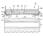
- FIG. 16A is a diagram schematically illustrating a planar layout of a sensor chip included in a conventional commercial product.
- FIG. 16A is a diagram schematically illustrating a planar layout of a sensor chip included in a conventional commercial product.
- FIG. 16B is a diagram showing a cross section taken along line BB in FIG. It is a figure which shows the cross section (substantially along an artery) perpendicular
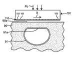
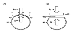
- FIG. 19A is a diagram schematically illustrating the relationship between the external pressure Po and the internal pressure Pi of the blood vessel when a flat portion is not formed in the artery.
- FIG. 19B is a diagram schematically showing the relationship between the external pressure Po and the internal pressure Pi of the blood vessel when a flat portion is formed in the artery.
- FIG. 1 and 2 show the appearance of a pulse wave detection device 100 according to an embodiment of the present invention.
- This pulse wave detection device 100 includes a sensor unit 1 mounted on the wrist surface for detecting a pulse wave in a wrist artery, a fixing base 2 for fixing the wrist for pulse wave detection, and a pulse wave detection.
- Display unit 3 (see FIG. 9) for inputting / outputting various types of information.
- the sensor unit 1 is accommodated in a substantially J-shaped housing 1M.
- FIG. 2 the sensor unit 1 is slid outside from the housing 1M through the slide groove 9, and the wrist is measured through the window 1W.
- a state of being positioned on a site the surface on the palm side through which the radial artery passes) 90 is shown.
- the fixed base 2 includes a fixed base unit 7, and the fixed base unit 7 and the display unit 3 are connected via a USB (Universal (Serial Bus) cable 4 so that they can communicate with each other.
- the fixed base unit 7 and the sensor unit 1 are connected via a communication cable 5 and an air pipe 6. *
- the user places the sensor unit 1 on the measured portion 90 of the wrist by sliding and moving the sensor unit 1 with the wrist placed on the fixed base 2 at a predetermined position.
- the housing 1M and the fixing base 2 are tightened through the belt 8 so that the sensor unit 1 on the wrist is not displaced.
- a pressure sensor (strain sensor) array 40 is provided on the side that contacts the wrist of the sensor unit 1 (the back side of the sensor unit 1 in FIGS. 1 and 2) by MEMS (Micro Electro Mechanical Systems) technology. And a pressing cuff 18 for pressing the sensor chip 19 toward the measurement site 90 of the wrist.
- MEMS Micro Electro Mechanical Systems
- the pressing cuff 18 receives the adjustment of the cuff pressure by the pressurizing pump 15 and the negative pressure pump 16 described later, and the direction in which the sensor chip 19 protrudes from the sensor unit 1 by an amount corresponding to the cuff pressure level (or vice versa). Direction). Thereby, the sensor chip 19 protrudes from the window 1W provided in advance in the housing 1M and is pressed against the measurement site 90.
- FIG. 5 schematically shows a planar layout of the sensor chip 19.
- the sensor chip 19 includes a silicon substrate 10 as a substantially flat substrate elongated in one direction (X direction), and is configured as an ASIC (Application Specific Integrated Circuit).
- the dimension of the silicon substrate 10 in the X direction is about 10 mm
- the dimension in the Y direction perpendicular to the X direction is about 3 mm
- the dimension (thickness) in the Z direction perpendicular to the X and Y directions is about 0.4 mm. Is set.
- a pressure sensor array 40 extending along the X direction is formed substantially in the center with respect to the Y direction of the silicon substrate 10.
- multiplexers 20A and 20B are formed which extend in parallel along the X direction.
- the electrode terminal array 50A, 50B is formed in the region facing the end of the pressure sensor array 40 on the silicon substrate 10, that is, in this example, the region along the short sides 10c and 10d on both sides in the X direction (shown by two-dot chain lines).
- a low-pass filter (LPF) 42 and an amplifier (hereinafter referred to as “amplifier”) 21 are formed in the vicinity of the electrode terminal array 50B on the + X side.
- the silicon substrate 10 is provided with a wiring (not shown) for connecting these parts 40, 20A, 20B, 42, 21, 50A, 50B.
- Regions 10A and 10B (shown by broken lines) corresponding to both sides of the pressure sensor array 40 in the Y direction are substantially flat surfaces where no electrode terminals are present.
- the pressure sensor array 40 includes a plurality (46 in this example) of pressure sensor (strain sensor) elements 41, 41,... Arranged at a constant pitch (in this example, 0.2 mm pitch) along the X direction.
- the pressure sensor array 40 is formed in a thin region 49 provided by cutting the back surface side ( ⁇ Z side) of the silicon substrate 10 into a concave shape.
- Each pressure sensor element 41 is of a known type including a Wheatstone bridge.
- the multiplexer 20 selects outputs A, B, C,... Of a plurality of pressure sensor elements 41, 41,.
- outputs (pressure signals) Ps1, Ps2,... Of the reduced number of pressure sensor elements are taken out in a time division manner.
- the number of pressure signals taken out is called “channel number”.
- the number of channels is 40 (three pressure sensor elements 41 at both ends of the pressure sensor array 40 are not used).
- 46 pressure sensor elements 41, 41,... Included in the pressure sensor array 40 may be used every two, and the number of channels may be 15 (one end of the pressure sensor array 40). Pressure sensor element 41 is not used.) In that case, the pitch of the pressure sensor elements 41, 41,... Used is substantially 0.6 mm.
- the low-pass filter 42 has a cutoff frequency of 500 kHz, removes high-frequency noise exceeding 500 kHz from the output of the multiplexer 20, and sends a signal of 500 kHz or less to the amplifier 21.
- the amplifier 21 amplifies Ps1, Ps2,..., The pressure signal received from the multiplexer 20 through the low-pass filter 42.
- the amplified pressure signals Ps1, Ps2,... Are output to the outside of the chip via an electrode terminal array (in this example, the electrode terminal array 50B in FIG. 5). Since the amplifier 21 is a chopper amplifier, a low-pass filter (not shown) for reducing noise associated with the chopper is included in the subsequent stage of the amplifier 21.
- the electrode terminal array 50A includes a plurality of electrode terminals E1, E2,..., E11 arranged in a line along the Y direction.
- the electrode terminal array 50B includes a plurality of electrode terminals E12, E13,..., E28 arranged in a line along the Y direction.
- each electrode terminal has a form of a flat aluminum electrode pad having dimensions in the X and Y directions of about 100 ⁇ m.
- the electrode terminal E1 is a terminal that receives a signal for activating (supplying power) all the pressure sensor elements 41, 41,.
- the electrode terminal E ⁇ b> 2 is a terminal that supplies power to the multiplexer 20 and the amplifier 21.
- the electrode terminal E3 is a terminal to which a ground potential is supplied.
- the electrode terminals E6 to E11 are terminals that receive signals for controlling the operation of the multiplexer 20 from the CPU 11.
- the electrode terminals E12, E13 are terminals for outputting pressure signals Ps1, Ps2,... Selected by the multiplexer 20 (after amplification by the amplifier 21) to the outside of the chip in a multi-scan mode to be described later.
- the electrode terminals E12 and E13 are terminals for outputting a pressure signal of a channel determined as an optimum channel among a plurality of channels to the outside of the chip in a channel fixing mode described later.
- the output of the pressure sensor element 41 of the pressure sensor array 40 is processed in the regions 10A and 10B corresponding to both sides of the pressure sensor array 40 of the silicon substrate 10 to thereby form the electrode terminal array 50B.
- the processing circuits 20, 42, and 21 to be sent to the electrode terminals are integrally formed. Therefore, it is not necessary to provide the processing circuit outside the chip, and the circuit outside the chip is simplified.
- the processing circuit selects the outputs of the plurality of pressure sensor elements 41 of the pressure sensor array 40, and the multiplexer 20 extracts the outputs (pressure signals) Ps1, Ps2,. Contains.
- the processing circuit selects the outputs of the plurality of pressure sensor elements 41 of the pressure sensor array 40, and the multiplexer 20 extracts the outputs (pressure signals) Ps1, Ps2,. Contains.
- the layout (the layout of FIG. 5) in which the electrode terminal array is arranged on the silicon substrate 10 along the direction (Y direction) perpendicular to the longitudinal direction (X direction) of the sensor chip 19 is facilitated and manufactured. Yield is improved.
- the number of output signals of the pressure sensor element 41 is reduced and the circuit outside the chip is simplified, so that the cost can be reduced.
- Electrode terminals included in the electrode terminal arrays 50A and 50B those not described for use include terminals for characteristic tests at the prototype stage of the sensor chip 19. Those characteristic test terminals can be omitted in the product stage.
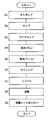
- FIG. 7 shows a mounting procedure of the sensor chip 19. i) First, as shown in step S1 of FIG. 7, in this example, the sensor chips 19, 19,... are placed on the upper surface 30a of the ceramic substrate 30 as shown in FIG. Die bonding is performed using a die bonding resin (not shown).
- FIG. 6A cross section along the extending direction of the pressure sensor array 40
- FIG. 6B cross section perpendicular to the extending direction of the pressure sensor array 40
- the ceramic substrate 30 In addition, the flexible wiring board 31), which will be described later, allows air to flow between the thin region (concave portion) 49 and the outside so as not to hinder the bending of the pressure sensor element 41 in the Z direction corresponding to each sensor chip 19.
- a through hole 39 is formed.
- step S2 of FIG. 7 curing (heat treatment) is performed to cure the die bond resin.
- the sensor chips 19, 19,... are fixed on the ceramic substrate 30.
- step S3 gold wire 32
- the sensor chip 19 and the ceramic substrate 30 are electrically connected.
- the gold wire 32 is provided with higher accuracy than the connection by the gold bump. As a result, the yield of this mounting process is improved.
- An electrode pad 38 for connection to a flexible wiring board 31 described later is formed on the lower surface 30b of the ceramic substrate 30.
- the electrode pads 37 and 38 on the upper and lower surfaces of the ceramic substrate 30 are electrically connected to each other through via holes (through holes) (not shown).
- a flow preventing resin so as to protect the gold wire 32 along the short sides 10c, 10d on both sides of the sensor chip 19 in the X direction.
- 33 and 34 are applied (step S4 in FIG. 7).
- the dam resin 33 is applied to the upper surface 19 a of the sensor chip 19, while the dam resin 34 is applied to the upper surface 30 a of the ceramic substrate 30.
- the height of the top portions of the dam resins 33 and 34 is set so as to slightly exceed the height of the top portion of the loop of the gold wire 32.
- a wire protecting resin (fill resin) 35 is applied so as to fill the gap between the respective dam resins 33 and 34 and wrap the gold wire 32. (Step S5 in FIG. 7). As a result, the gold wire 32 is protected by being wrapped in the fill resin 35.
- the ceramic substrate 30 is cut in the X and Y directions along the dicing lines DL, and the ceramic substrate 30 and the sensor chip 19 are separated. These are integrated into individual pieces (step S6 in FIG. 7).
- step S8 of FIG. 7 this subassembly is mounted on the sensor unit 1 (see FIG. 3).
- the connector 51 of the flexible wiring board (FPC) 31 is electrically connected to a corresponding connector (not shown) of the sensor unit 1.
- the ceramic substrate 30 and the flexible wiring board (FPC) 31 constitute a wiring board.
- a protective sheet 60 (for example, shown in FIG. 11) is attached so as to cover the sensor unit 1, particularly the sensor chip 19 (mounting is completed).
- the protective sheet 60 is made of a silicone resin sheet having a thickness of about 150 ⁇ m to 300 ⁇ m.
- the regions 10A and 10B corresponding to both sides of the pressure sensor array 40 of the sensor chip 19 are flat surfaces where no electrode terminals are present. Therefore, the outer surface 60a of the protective sheet 60 that is pressed against the measurement site 90 is also a flat surface.
- the electrode terminal arrays 50 ⁇ / b> A and 50 ⁇ / b> B exist in a region facing the end of the pressure sensor array 40 of the sensor chip 19.
- fill resin 35 and the dam resins 33 and 34 bulge outwardly (measured portion 90), the fill resin 35 and the like of the protective sheet 60
- the portions 60c and 60d corresponding to the bulge are also raised outward.
- the longitudinal direction of the sensor chip 19, that is, the extending direction of the pressure sensor array 40 is arranged so as to intersect the artery 91.
- FIG. 9 shows a functional block configuration of the pulse wave detection device 100.
- the block configuration of the pulse wave detection device 100 is roughly divided into the sensor unit 1 described above, the fixed base unit 7 included in the fixed base 2, and the display unit 3.
- the display unit 3 is provided so as to be operable from the outside and is operated to input various information related to pulse wave detection, and outputs various information such as an arterial position detection result and a pulse wave measurement result to the outside.
- a display unit 25 including an LED (Light Emitting Diode) and an LCD (Liquid Crystal Display).
- the fixed base unit 7 concentrates a ROM (Read Only Memory) 12 and a RAM (Random Access Memory) 13 for storing data and programs for controlling the pulse wave detecting device 100 and the pulse wave detecting device 100 in a concentrated manner.
- a CPU (Central Processing Unit) 11 that executes various processes including operations for control, a pressure pump 15, a negative pressure pump 16, a switching valve 17, and a control signal from the CPU 11 are received.
- the control circuit 14 for controlling the pressurizing pump 15, the negative pressure pump 16, and the switching valve 17, the characteristic variable filter 22, and the A / D converter 23 are provided.
- the CPU 11 accesses the ROM 12, reads out the program, develops it on the RAM 13, executes it, receives an operation signal from the user from the operation unit 24, and controls the entire pulse wave detection device 100 based on the operation signal. Do. In particular, the CPU 11 sends a control signal for controlling the pressurization pump 15, the negative pressure pump 16, and the switching valve 17 to the control circuit 14 based on the operation signal input from the operation unit 24. Further, the CPU 11 displays the pulse wave measurement result and the like on the display unit 25.
- the pressurizing pump 15 is a pump for pressurizing the internal pressure (hereinafter referred to as “cuff pressure”) of the pressing cuff (air bag) 18, and the negative pressure pump 16 is a pump for reducing the cuff pressure.
- the switching valve 17 selectively connects one of the pressurizing pump 15 and the negative pressure pump 16 to the air pipe 6.
- the control circuit 14 controls the pressurizing pump 15, the negative pressure pump 16, and the switching valve 17 based on a control signal from the CPU 11.
- the sensor unit 1 includes the above-described sensor chip 19 and a pressure cuff 18 including an air bag that is pressure-adjusted to press the sensor chip 19 onto the wrist.
- the characteristic variable filter 22 included in the fixed base unit 7 is a low-pass filter for blocking a signal component having a cutoff frequency fc or higher.
- the characteristic variable filter 22 includes a variable capacitance diode whose capacity is controlled by a filter characteristic control voltage from the CPU 11, and is called two characteristics (respectively “characteristic A” and “characteristic B”) having different cutoff frequencies fc. .)
- the characteristic A is a state in which the cutoff frequency fc is set to a value fcA that is equal to or higher than the switching frequency fx (20 kHz in this example) when scanning the plurality of pressure sensor elements 41, 41,. .
- Characteristic B is a state in which the cutoff frequency fc is set to a value fcB lower than 1 ⁇ 2 of the sampling frequency fs of the pressure signal from one pressure sensor element. For example, if the switching frequency fx when scanning the pressure signals Ps1, Ps2,..., Ps40 from the 40-channel pressure sensor elements 41, 41,... Is 20 kHz, the sampling frequency of the pressure signal from one pressure sensor element. fs is 500 Hz.
- fcA 250 kHz is set.
- the A / D conversion unit 23 converts the pressure signal, which is an analog signal derived from the sensor chip 19, into digital information and gives it to the CPU 11. As a result, the CPU 11 can acquire the pressure signals Ps1, Ps2,... Output from the plurality of pressure sensor elements 41, 41,.
- FIG. 10 shows a flow of measurement processing by the pulse wave detection device 100.
- the measurement process shown in this flow is realized by the CPU 11 accessing the ROM 22 to read out the program, developing it on the RAM 23 and executing it.
- the CPU 11 instructs the control circuit 14 to drive the negative pressure pump 16, and the control circuit 14 turns the switching valve 17 on the basis of this instruction.
- the negative pressure pump 16 is driven (S101).
- the cuff pressure is made sufficiently lower than the atmospheric pressure via the switching valve 17, and the sensor chip 19 protrudes carelessly from the sensor unit 1 and malfunctions or breaks down. Can be avoided.
- the housing 1M includes a micro switch (not shown) for detecting the movement of the sensor unit 1, and the CPU 11 determines whether the sensor unit 1 has moved based on the detection signal of the micro switch.
- the CPU 11 When it is determined that measurement is started (YES in S103), the CPU 11 operates the multiplexer 20 to start a channel scan in order to obtain pressure signals from the pressure sensor elements 41, 41,... (S105). This is called a multi-scan mode. In this multi-scan mode, the CPU 11 switches the characteristic variable filter 22 to the characteristic A by the filter characteristic control signal and sets its cutoff frequency to fcA (S107). Since fcA is a value equal to or higher than the switching frequency fx of the pressure signal from the plurality of pressure sensor elements 41, 41,..., Curling can be prevented from occurring during waveform restoration.
- the CPU 11 sends a control signal to the control circuit 14 so as to drive the pressure pump 15. Based on this control signal, the control circuit 14 switches the switching valve 17 to the pressurizing pump 15 side and drives the pressurizing pump 15 (S109). Thereby, the cuff pressure rises and the sensor chip 19 of the sensor unit 1 is pressed against the surface of the measurement site 90 of the subject.
- the longitudinal direction of the sensor chip 19, that is, the extending direction of the pressure sensor array 40 is arranged so as to intersect the artery 91.
- the pressure signals from the pressure sensor elements 41, 41,... Included in the sensor chip 19 are time-divided in the multiplexer 20 and amplified in the amplifier 21 through the low-pass filter 42. Is done. Thereafter, the amplified pressure signal is input to the characteristic variable filter 22. Then, the pressure signal filtered by the characteristic variable filter 22 is sent to the A / D converter 23. Then, it is converted into digital information by the A / D converter 23 and input to the CPU 11.
- the CPU 11 creates a tonogram (histogram representing the amplitude of the AC component (pulse wave signal) of the pressure signal) using these digital information and displays it on the display unit 25 (S111 in FIG. 10).
- FIG. 13A shows the waveforms of 40-channel pressure signals Ps1, Ps2,..., Ps40.
- the waveforms of the pressure signals Ps1, Ps2,..., Ps40 are drawn slightly shifted in the vertical direction for easy understanding.
- the tonogram is obtained as a histogram representing the amplitude (pulse wave amplitude) of the alternating current component (pulse wave signal) of these pressure signals Ps1, Ps2,..., Ps40, as shown in FIG.
- shaft of FIG.13 (B) represents the channel number corresponding to each pressure signal Ps1, Ps2, ..., Ps40.
- the CPU 11 indicates the maximum value of the pulse wave amplitude among the plurality of pressure sensor elements 41, 41,. Channel 8) is detected as being located on artery 91.
- the process for selecting the pressure sensor element located on the artery 91 as an optimal channel is performed (S113).
- a known technique described in Japanese Patent Application Laid-Open No. 2004-222847 can be used.
- one pressure sensor element (Di) is selected as the optimum channel (note that two or more optimum channels may be employed).
- the CPU 11 extracts the DC component from the pressure signal input from each pressure sensor element 41, 41,... In order to determine the optimum pressing force of the pressing cuff 18 (S115).
- the pressure signal Ps includes a DC component Pdc and an AC component (pulse wave signal) Pac.
- the DC component Pdc is the average value of the pressure signal over a certain period of time, the component of the pressure signal that has passed through the low-pass filter (the component from which the pulse wave has been removed), or the pressure at the pulse wave rising point (immediately before the pulse wave component is mixed) Determined by signal level.
- step S115 of FIG. 10 the change in the output of the pressure signal is divided into windows (sections) at certain time intervals, and the DC component Pdc is extracted by calculating the average in each window. it can.
- the DC component Pdc is extracted in the same manner even if an intermediate value between the maximum value and the minimum value in each window is calculated, or a value below a predetermined frequency is extracted using a low-pass filter. be able to.
- the above-mentioned fixed time is a time interval set in advance in the pulse wave detection device 100 that does not depend on the pulse of the subject, and may be about 1.5 seconds including a general pulse time. preferable.
- the CPU 11 detects a place where the DC component Pdc extracted in step S115 is stable based on the pressure signal input from each pressure sensor element 41, 41,... (S117). If the location where the DC component Pdc is stable is not detected (NO in S117), the location where the DC component Pdc is stable is detected while continuing to pressurize the pressure cuff 18 by the pressure pump 15. Up to this point, the processes in steps S111 to S117 are repeated.
- fcB is a value lower than 1/2 of the sampling frequency fs of the pressure signal from one pressure sensor element
- the sampling frequency is used when converting an analog signal into a digital signal by the sampling theorem.
- Noise having a frequency component equal to or higher than 1/2 of the sampling frequency may appear in a region less than 1/2 of the sampling frequency due to the aliasing phenomenon.
- a technique for removing the aliasing noise is described in, for example, Japanese Patent Application Laid-Open No. 2005-341994.
- the position where the DC component Pdc detected in step S117 is stable is once set as the optimum pressing force of the pressing cuff 18, and a control signal is sent to the control circuit 14 so as to adjust the pressure of the pressing cuff 18 ( S123).
- the optimum pressing force is obtained within the range of the frame AP.
- the CPU 11 rises the pressure signal output from the pressure sensor element Di selected as the optimum channel in the state where the pushing force of the pushing cuff 18 is kept at the optimum pressure, that is, the rising edge of the waveform data as illustrated in FIG. It is determined whether or not the point sharpness (MSP) is appropriate (S125), and whether or not there is waveform distortion (S127).
- MSP point sharpness
- S127 waveform distortion
- P1 indicates the peak of the ejection wave
- P2 indicates the peak of the reflected wave.
- the CPU 11 When the sharpness (MSP) of the rising point of the waveform data is appropriate (YES in S125) and no waveform distortion is detected (YES in S127), the CPU 11 performs the multiplexer 20, the amplifier 21, and the characteristic variable filter. 22 and the A / D converter 23 acquire waveform data at that time (S129).
- MSP sharpness
- the CPU 11 detects a pulse wave from the acquired waveform data and determines whether a predetermined condition for the end of the pulse wave detection is satisfied (S131).
- the condition for ending the pulse wave detection in step S131 may be a predetermined time (for example, 30 seconds) that has been set in advance, or an end (or interruption) instruction from the user. That is, the above-described pulse wave data transfer process in step S129 is repeated until a predetermined condition is satisfied.
- the CPU 11 sends a control signal to the control circuit 14 so as to drive the negative pressure pump 16 via the switching valve 17 (S133). . Thereby, the pressing state of the sensor chip 19 with respect to the measurement site 90 is released, and the series of pulse wave measurement processing ends.
- the outer surface 60a of the protective sheet 60 pressed against the measurement site 90 is also a flat surface. Therefore, there is no obstacle in flattening the outward portion 91a of the blood vessel wall of the artery 91. As a result, the outward portion 91a of the blood vessel wall of the artery 91 can be flattened with high accuracy. Therefore, the change in the internal pressure of the artery 91 can be accurately obtained without being affected by the blood vessel wall.
- the electrode terminal arrays 50A and 50B are provided in the region of the sensor chip 19 facing the end of the pressure sensor array 40.
- the fill resin 35 and the like are raised in a convex shape toward the outside (measurement site 90).
- the electrode terminal arrays 50A and 50B, the fill resin 35, and the like exist in a region outside the artery 91, there is no obstacle to flattening the outward portion 91a of the blood vessel wall of the artery 91.
- the regions 10A and 10B there are no electrode terminal arrays in the regions 10A and 10B corresponding to both sides of the pressure sensor array 40 on the silicon substrate 10 of the sensor chip 19, so that both sides of the pressure sensor array 40 are provided.
- the dimensions of the corresponding regions 10A and 10B can be reduced.
- the low-pass filter 42 and the amplifier 21 may be provided outside the chip to simplify the processing circuit in the sensor chip 19. As a result, it is possible to reduce the pressing force on the measurement site 90 and thus reduce pain to the measurement subject.
- the silicon substrate 10 is used as the substrate constituting the sensor chip 19, but the present invention is not limited to this.
- the substrate may be any substrate as long as a pressure sensor (strain sensor) array can be formed by MEMS technology, and may be a substrate made of another material.
- the ceramic substrate 30 and the flexible wiring board 31 are used as the wiring substrate, but the present invention is not limited to this.
- the wiring board may support the board and may be provided with a wiring connected to the electrode terminal on the board, and may be a board made of another material.
- a part of the flexible wiring board 31 may be rigidly configured, and the sensor chip 19 may be directly mounted on the rigid part.
- the protective sheet 60 is provided so as to cover the sensor chip 19, but the present invention is not limited to this.
- the surface of the sensor chip 19 together with the gold wire 32 may be coated with a resin to be substantially flat and sealed for protection.
- the electrode terminals included in the electrode terminal arrays 50A and 50B are arranged in a line along the Y direction.
- the electrode terminal arrays 50 ⁇ / b> A and 50 ⁇ / b> B may be provided in a region facing the end of the pressure sensor array 40.
- the electrode terminal arrays 50A and 50B may be arranged in two rows along the Y direction, and are shifted from each other by 1 ⁇ 2 pitch (so-called staggered arrangement). In such a case, the Y-direction dimension of the sensor chip 19 can be reduced as compared with the case of one row.
Landscapes
- Health & Medical Sciences (AREA)
- Life Sciences & Earth Sciences (AREA)
- Engineering & Computer Science (AREA)
- General Health & Medical Sciences (AREA)
- Veterinary Medicine (AREA)
- Biophysics (AREA)
- Biomedical Technology (AREA)
- Heart & Thoracic Surgery (AREA)
- Medical Informatics (AREA)
- Molecular Biology (AREA)
- Surgery (AREA)
- Animal Behavior & Ethology (AREA)
- Physics & Mathematics (AREA)
- Public Health (AREA)
- Pathology (AREA)
- Cardiology (AREA)
- Physiology (AREA)
- Signal Processing (AREA)
- Artificial Intelligence (AREA)
- Computer Vision & Pattern Recognition (AREA)
- Psychiatry (AREA)
- Power Engineering (AREA)
- Vascular Medicine (AREA)
- Measuring Pulse, Heart Rate, Blood Pressure Or Blood Flow (AREA)
Abstract
本発明の脈波検出装置では、センサチップは、X方向に細長く延在する形状をもち、動脈に対して交差して配置される基板(10)を備える。基板(10)に、X方向に沿って並ぶ複数の圧力センサ素子(41)からなる圧力センサアレイ(40)が形成されている。基板(10)上で圧力センサアレイ(40)の端部に対向する領域に、複数の圧力センサ素子(41)の出力をチップ外へ取り出すための電極端子アレイ(50B)が形成されている。基板(10)上で圧力センサアレイ(40)の両側に相当する領域(10A,10B)は、電極端子が存在しない平坦面になっている。
Description
この発明は脈波検出装置に関し、より詳しくは、圧力センサ(歪みセンサ)アレイが形成されたセンサチップを動脈が通る被測定部位に押しつけて、非観血式に脈波を検出する脈波検出装置に関する。
この種の脈波検出装置としては、例えば特許文献1(特開2011-239840号公報)に示すように、MEMS(Micro Electro Mechanical Systems)技術によって圧力センサ(歪みセンサ)アレイが形成されたセンサチップを動脈が通る被測定部位に押しつけて、トノメトリ法により非観血式に、上記動脈の内圧の変化、つまり脈波を測定するものが知られている。
トノメトリ法により非観血式に血圧(動脈の内圧の変化を含む。)を測定するための市販品では、図16(A)に示すようにパターンレイアウトされたセンサチップを備えたものがある。この例では、センサチップ101は、一方向(X方向)に細長い略平板状のシリコン基板102と、このシリコン基板102のY方向(X方向に対して垂直な方向)に関して略中央に形成された圧力センサアレイ110と、Y方向に関して両側の長辺102a,102bに沿って形成された電極端子アレイ120A,120Bとを備えている。圧力センサアレイ110は、X方向に沿って一定ピッチで並ぶ複数の圧力センサ(歪みセンサ)素子111からなっている。電極端子アレイ120A,120Bは、それぞれX方向に沿って一定ピッチで並ぶ複数の金バンプ電極121,121,…からなっている。圧力センサアレイ110の各圧力センサ素子111は、シリコン基板102上に形成された図示しない配線を介して、電極端子アレイ120A,120Bの対応する金バンプ電極121と接続されている。図16(B)(図16(A)におけるB-B線断面)に示すように、圧力センサアレイ110は、シリコン基板102の裏面側(-Z側)を凹状に削って設けられた薄厚領域119に形成されている。シリコン基板102の裏面側は、ガラス板103によって支持されている。ガラス板103には、圧力センサ素子111のZ方向の撓みを妨げないように、薄厚領域(凹部)119と外部との空気の流通を許す貫通孔103A,103Bが設けられている。
図17中に示すように、センサチップ101を実装した製品では、電極端子アレイ120A,120Bの金バンプ電極121,121にフレキシブル配線板130A,130Bが接続されている。フレキシブル配線板130A,130Bには、各圧力センサ素子111からの信号を処理する処理回路(図示せず)が搭載されている。また、センサチップ101の表面全域を覆う樹脂からなる保護シート140が設けられている。
トノメトリ法による血圧測定時には、図18中に示すように、センサチップ101は、動脈91が通る被測定部位90に対して押しつけられる。これにより、センサチップ101を介して外圧Poによって動脈91を圧迫して、動脈91を完全に潰しきることなく、動脈91の血管壁の一部(センサチップ101に対向する体表面90aに近い部分。以下「外向き部分」という。)91aのみを平坦な状態にする。すなわち、その外向き部分91aの血管壁の曲率半径を無限大にする。このとき、センサチップ101の長手方向、すなわち、圧力センサアレイ110の延在方向(X方向)が、動脈91に対して交差する向きに配置される。この配置で、圧力センサアレイ110が含む複数の圧力センサ素子111,111,…の出力に基づいて、圧力センサアレイ110の中で適切な圧力センサ素子111が選択される。そして、その選択された圧力センサ素子111の出力に基づいて、動脈91の内圧の変化が測定される。
具体的には、図19(B)に模式的に示すように、外圧Poと血管の内圧Piとの平衡を保ちながら、外圧Poに抗して拍動する内圧(血圧脈波)Piが求められる。なお、図19(A)に模式的に示すように、動脈91に平坦な部分が形成されない場合は、外圧Poと内圧Piとの関係式
Po=Pi+T/r
において、血管壁の曲率半径(rとする。)が比較的小さくなる。このため、外圧Poと血管の内圧Piとが実質的に一致せず、正確な測定が行われない。
Po=Pi+T/r
において、血管壁の曲率半径(rとする。)が比較的小さくなる。このため、外圧Poと血管の内圧Piとが実質的に一致せず、正確な測定が行われない。
従来の市販品では、図17に示すように圧力センサアレイ110の延在方向に対して垂直な断面(実質的に動脈91に沿った断面)を見た場合、センサチップ101の両側の長辺102a,102bの近傍に、金バンプ電極121,121とそれに接続されたフレキシブル配線板130A,130Bが存在するため、保護シート140のうち両側の長辺102a,102b近傍の部分140a,140bが矢印Eで示すように外(被測定部位90)へ向かって凸状に盛り上がっている。このため、動脈91の血管壁の外向き部分91aを平坦化するのに、その凸状に盛り上がった部分140a,140bが障害になるという問題がある。この結果、曲率半径を無限大にすることが出来ず、血管壁張力の影響を受けて、測定精度が低下する可能性がある。
そこで、この発明の課題は、圧力センサアレイが形成されたセンサチップを動脈が通る被測定部位に押しつけて、非観血式に脈波を検出する脈波検出装置であって、動脈の血管壁の外向き部分を精度良く平坦化でき、したがって血管の内圧を正確に求めることができるものを提供することにある。
上記課題を解決するため、この発明の脈波検出装置は、
圧力センサアレイが形成されたセンサチップを動脈が通る被測定部位に押しつけて、非観血式に脈波を検出する脈波検出装置であって、
上記センサチップは、
一方向に細長く延在する形状をもち、上記動脈に対して交差して配置される基板と、
この基板に形成された、上記一方向に沿って並ぶ複数の圧力センサ素子からなる圧力センサアレイと、
上記基板上で上記圧力センサアレイの端部に対向する領域に形成された、上記複数の圧力センサ素子の出力をチップ外へ取り出すための、上記一方向に対して垂直な方向に沿って並ぶ複数の電極端子からなる電極端子アレイとを備え、
上記基板上で上記圧力センサアレイの両側に相当する領域は、電極端子が存在しない実質的な平坦面になっていることを特徴とする。
圧力センサアレイが形成されたセンサチップを動脈が通る被測定部位に押しつけて、非観血式に脈波を検出する脈波検出装置であって、
上記センサチップは、
一方向に細長く延在する形状をもち、上記動脈に対して交差して配置される基板と、
この基板に形成された、上記一方向に沿って並ぶ複数の圧力センサ素子からなる圧力センサアレイと、
上記基板上で上記圧力センサアレイの端部に対向する領域に形成された、上記複数の圧力センサ素子の出力をチップ外へ取り出すための、上記一方向に対して垂直な方向に沿って並ぶ複数の電極端子からなる電極端子アレイとを備え、
上記基板上で上記圧力センサアレイの両側に相当する領域は、電極端子が存在しない実質的な平坦面になっていることを特徴とする。
本明細書で「実質的な平坦面」とは、センサチップを動脈が通る被測定部位に押しつけるときに平坦であると感じられれば足り、ミクロンオーダの微細な凹凸(例えばセンサチップを作製する半導体プロセスで生じるような薄膜の段差)を許容する意味である。
この発明の脈波検出装置では、血圧測定時には、上記センサチップは、動脈が通る被測定部位に対して押しつけられる。このとき、上記センサチップの長手方向、すなわち、上記圧力センサアレイの延在方向が、上記動脈に対して交差して配置される。そして、上記圧力センサアレイが含む複数の圧力センサ素子の出力に基づいて、上記圧力センサアレイの中で適切な圧力センサ素子(例えば、最も大きい脈波信号を出力するもの)が選択される。そして、その選択された圧力センサ素子の出力に基づいて、上記動脈の内圧の変化(つまり、脈波)が測定される。
ここで、この脈波検出装置では、上記複数の圧力センサ素子の出力は、上記基板上で上記圧力センサアレイの端部に対向する領域に形成された電極端子アレイを介して、チップ外へ取り出される。上記基板上で上記圧力センサアレイの両側に相当する領域は、電極端子が存在しない実質的な平坦面になっている。したがって、上記圧力センサアレイの延在方向に対して垂直な断面(実質的に上記動脈に沿った断面)では、上記動脈の血管壁の外向き部分を平坦化するのに障害が存在しない。この結果、上記動脈の血管壁の外向き部分を精度良く平坦化できる。したがって、血管壁の影響を受けず、上記動脈の内圧の変化を正確に求めることができる。
なお、上記圧力センサアレイの延在方向に沿った断面(上記動脈を横切る断面)では、上記基板上で上記圧力センサアレイの端部に対向する領域に電極端子が存在する。しかし、この電極端子は上記動脈から外れた領域に存在するので、上記動脈の血管壁の外向き部分を平坦化するのに障害にはならない。
また、上記センサチップの上記基板上で上記圧力センサアレイの両側に相当する領域には、電極端子アレイが存在しない。したがって、上記圧力センサアレイの延在方向に対して垂直な断面(実質的に上記動脈に沿った断面)において、上記圧力センサアレイの両側に相当する領域の寸法を小さくすることができる。この結果、被測定部位に対する圧迫力を小さくでき、したがって被測定者に対する苦痛を低減できる。
一実施形態の脈波検出装置では、上記電極端子アレイは、上記一方向に対して垂直な方向に沿って並ぶ複数の電極端子を含むことを特徴とする。
この一実施形態の脈波検出装置では、複数の電極端子を上記一方向に沿って並べる配置に比して、上記センサチップの上記一方向の寸法が大きくなるのを抑制できる。
一実施形態の脈波検出装置では、上記基板の上記圧力センサアレイの両側に相当する領域に、上記圧力センサアレイの上記圧力センサ素子の出力を処理して、上記電極端子アレイの電極端子へ送出する処理回路が一体に形成されていることを特徴とする。
この一実施形態の脈波検出装置では、上記基板の上記圧力センサアレイの両側に相当する領域に、上記圧力センサアレイの上記圧力センサ素子の出力を処理して、上記電極端子アレイの電極端子へ送出する処理回路が一体に形成されている。したがって、上記処理回路をチップ外に設ける必要が無くなり、チップ外の回路が簡素化される。
一実施形態の脈波検出装置では、上記処理回路は、上記圧力センサアレイの上記複数の圧力センサ素子の出力を選択して、低減された数の圧力センサ素子の出力を時分割で取り出すマルチプレクサを含むことを特徴とする。
この一実施形態の脈波検出装置では、上記処理回路は、上記圧力センサアレイの上記複数の圧力センサ素子の出力を選択して、低減された数の圧力センサ素子の出力を時分割で取り出すマルチプレクサを含む。これにより、上記電極端子アレイが含む電極端子の数を低減することが可能になる。したがって、上記電極端子アレイを上記基板上で上記一方向(上記センサチップの長手方向)に対して垂直な方向に沿って配置するレイアウトが容易になるとともに、製造歩留が向上する。また、上記圧力センサ素子の出力信号数が低減されて、チップ外の回路が簡素化されるので、コストダウンが可能となる。
一実施形態の脈波検出装置では、
上記センサチップを搭載して支持する配線基板を備え、
上記センサチップの上記電極端子アレイの電極端子は、上記配線基板上の対応する電極パッドに、ワイヤを介して接続されていることを特徴とする。
上記センサチップを搭載して支持する配線基板を備え、
上記センサチップの上記電極端子アレイの電極端子は、上記配線基板上の対応する電極パッドに、ワイヤを介して接続されていることを特徴とする。
この一実施形態の脈波検出装置では、上記センサチップの上記電極端子アレイの電極端子は、上記配線基板上の対応する電極パッドに、ワイヤを介して接続されている。このワイヤは、公知のワイヤボンディング技術によって、金バンプによる接続に比して精度良く設けられる。この結果、実装工程の歩留りが向上する。
一実施形態の脈波検出装置では、上記ワイヤは樹脂で封止されていることを特徴とする。
この一実施形態の脈波検出装置では、上記ワイヤは樹脂で封止されている。したがって、上記ワイヤが上記樹脂によって保護される。
以上より明らかなように、この発明の脈波検出装置によれば、動脈の血管壁の外向き部分を精度良く平坦化でき、したがって血管の内圧を正確に求めることができる。
以下、この発明の実施の形態を、図面を参照しながら詳細に説明する。
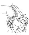
図1および図2は、この発明の一実施形態の脈波検出装置100の外観を示している。この脈波検出装置100は、手首の動脈における脈波を検出するために手首表面に装着されるセンサユニット1と、脈波検出のために手首を固定するための固定台2と、脈波検出に関する各種情報を入出力するための表示ユニット3(図9参照)とを備える。図1ではセンサユニット1は略J字状の筐体1M内に収容されており、図2ではスライド溝9を介して筐体1M内から外部にスライド移動されて、窓1Wを通して手首の被測定部位(橈骨動脈が通っている手のひら側の表面)90上に位置している状態が示される。
固定台2は固定台ユニット7を内蔵しており、固定台ユニット7と表示ユニット3とはUSB(Universal Serial Bus)ケーブル4を介して通信可能に接続される。また、固定台ユニット7とセンサユニット1とは通信ケーブル5とエア管6とを介して接続される。
脈波検出時には、図2に示すように、ユーザは手首を固定台2の所定位置に載置した状態で、センサユニット1をスライド移動により手首の被測定部位90に位置させてセンサユニット1の筐体1Mと固定台2とをベルト8を介して締めて、手首上のセンサユニット1がずれないように止める。
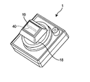
図3に示すように、センサユニット1の手首に当接される側(図1、2におけるセンサユニット1の裏側)には、MEMS(Micro Electro Mechanical Systems)技術によって圧力センサ(歪みセンサ)アレイ40が形成されたセンサチップ19と、このセンサチップ19を手首の被測定部位90へ向けて押圧するための押圧カフ18とが設けられている。
押圧カフ18は、後述の加圧ポンプ15および負圧ポンプ16によるカフ圧の調整を受けて、このカフ圧レベルに応じた量だけセンサチップ19をセンサユニット1から突出する向き(またはその逆の向き)に移動させる。これにより、センサチップ19は、筐体1Mの予め設けられた窓1Wから突出して被測定部位90に押圧される。
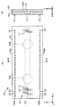
図5は、上記センサチップ19の平面レイアウトを模式的に示している。このセンサチップ19は、一方向(X方向)に細長い略平板状の基板としてのシリコン基板10を備え、ASIC(Application Specific Integrated Circuit)として構成されている。シリコン基板10のX方向の寸法は10mm程度、X方向に対して垂直なY方向の寸法は3mm程度、X,Y方向に対して垂直なZ方向の寸法(厚さ)は0.4mm程度に設定されている。このシリコン基板10のY方向に関して略中央に、X方向に沿って延在する圧力センサアレイ40が形成されている。この圧力センサアレイ40の両側に、それぞれX方向に沿って平行に延在するマルチプレクサ20A,20B(適宜、符号20で総称する。)が形成されている。シリコン基板10上で圧力センサアレイ40の端部に対向する領域、すなわち、この例ではX方向に関して両側の短辺10c,10dに沿った領域(2点鎖線で示す)に、電極端子アレイ50A,50Bが形成されている。図5において+X側の電極端子アレイ50Bの近傍に、ローパスフィルタ(LPF)42と、増幅器(以下「アンプ」という。)21とが形成されている。また、シリコン基板10には、これらの各部40,20A,20B,42,21,50A,50Bを接続する図示しない配線が設けられている。Y方向に関して圧力センサアレイ40の両側に相当する領域(破線で示す)10A,10Bは、電極端子が存在しない実質的な平坦面になっている。
圧力センサアレイ40は、X方向に沿って一定ピッチ(この例では0.2mmピッチ)で並ぶ複数(この例では46個)の圧力センサ(歪みセンサ)素子41,41,…を含んでいる。例えば図6(A),図6(B)中に示すように、圧力センサアレイ40は、シリコン基板10の裏面側(-Z側)を凹状に削って設けられた薄厚領域49に形成されている。各圧力センサ素子41は、ホイーストンブリッジを含む公知のタイプのものである。
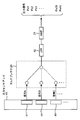
図8に示すように、マルチプレクサ20は、後述のCPU11による制御を受けて、圧力センサアレイ40に含まれた複数の圧力センサ素子41,41,…の出力A,B,C,…を選択して、低減された個数の圧力センサ素子の出力(圧力信号)Ps1,Ps2,…を時分割で取り出す。この取り出される圧力信号の数を「チャネル数」と呼ぶ。この例では、チャネル数を40チャネルとする(圧力センサアレイ40の両端の3個ずつの圧力センサ素子41が使用されない。)。
なお、例えば圧力センサアレイ40に含まれ46個の圧力センサ素子41,41,…を2個おきに使用して、チャネル数を15チャネルとしてもよい(圧力センサアレイ40の端部の1個の圧力センサ素子41が使用されない。)。その場合、使用される圧力センサ素子41,41,…のピッチは、実質的に0.6mmピッチとなる。
ローパスフィルタ42は、この例では遮断周波数500kHzのものであり、マルチプレクサ20の出力から500kHzを超える高周波ノイズを除去して、500kHz以下の信号をアンプ21へ送る。
アンプ21は、マルチプレクサ20からローパスフィルタ42を通して受けた圧力信号をPs1,Ps2,…を増幅する。増幅された圧力信号Ps1,Ps2,…は、電極端子アレイ(この例では、図5中の電極端子アレイ50B)を介してチップ外へ出力される。なお、アンプ21はチョッパアンプであるため、アンプ21の後段には、チョッパに伴う雑音を低減するためのローパスフィルタ(図示せず)が含まれている。
図5中に示すように、電極端子アレイ50Aは、Y方向に沿って1列に並ぶ複数の電極端子E1,E2,…,E11を含んでいる。同様に、電極端子アレイ50BはY方向に沿って1列に並ぶ複数の電極端子E12,E13,…,E28を含んでいる。このように、複数の電極端子をY方向に沿って1列に並べることによって、X方向寸法の増加を抑制している。この例では、各電極端子は、X,Y方向の寸法が100μm程度の平坦なアルミニウム電極パッドの形態を有している。
例えば、電極端子E1は、後述のCPU11から、全ての圧力センサ素子41,41,…(のホイーストンブリッジ)を活性化(電力を供給)する信号を受ける端子である。電極端子E2は、マルチプレクサ20およびアンプ21に電力を供給する端子である。電極端子E3は、接地電位が供給される端子である。電極端子E6~E11は、CPU11からマルチプレクサ20の動作を制御する信号を受ける端子である。電極端子E6~E11に受ける信号のコード(高レベル、低レベルの組み合わせ)によって、複数の圧力センサ素子41,41,…の出力(圧力信号)のうちマルチプレクサ20が選択して取り出すべき圧力信号が定まる。電極端子E12,E13は、後述のマルチスキャンモードで、マルチプレクサ20によって選択された(アンプ21による増幅後の)圧力信号Ps1,Ps2,…をチップ外へ出力する端子である。また、電極端子E12,E13は、複数のチャネルのうち最適チャネルとして決定されたチャネルの圧力信号を、後述のチャネル固定モードでチップ外へ出力する端子である。
上述のように、このセンサチップ19では、シリコン基板10の圧力センサアレイ40の両側に相当する領域10A,10Bに、圧力センサアレイ40の圧力センサ素子41の出力を処理して、電極端子アレイ50Bの電極端子へ送出する処理回路20,42,21が一体に形成されている。したがって、その処理回路をチップ外に設ける必要が無くなり、チップ外の回路が簡素化される。
また、その処理回路は、圧力センサアレイ40の複数の圧力センサ素子41の出力を選択して、低減された数の圧力センサ素子41の出力(圧力信号)Ps1,Ps2,…を取り出すマルチプレクサ20を含んでいる。これにより、電極端子アレイ50A,50Bが含む電極端子の数を低減することが可能になる。したがって、電極端子アレイをシリコン基板10上でセンサチップ19の長手方向(X方向)に対して垂直な方向(Y方向)に沿って配置するレイアウト(図5のレイアウト)が容易になるとともに、製造歩留が向上する。また、圧力センサ素子41の出力信号数が低減されて、チップ外の回路が簡素化されるので、コストダウンが可能となる。
なお、電極端子アレイ50A,50Bが含む電極端子のうち用途を説明していないものの中には、センサチップ19の試作段階における特性テスト用の端子も含まれている。それらの特性テスト用端子は、製品段階では省略され得る。
図7は、上記センサチップ19の実装手順を示している。
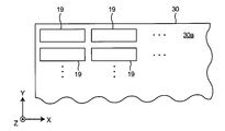
i) まず、図7のステップS1に示すように、この例では図4中に示すようなセラミック基板30の上面30aに、X,Y方向にそれぞれ一定ピッチでセンサチップ19,19,…を、ダイボンド樹脂(図示せず)を用いてダイボンドする。
i) まず、図7のステップS1に示すように、この例では図4中に示すようなセラミック基板30の上面30aに、X,Y方向にそれぞれ一定ピッチでセンサチップ19,19,…を、ダイボンド樹脂(図示せず)を用いてダイボンドする。
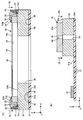
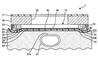
なお、図6(A)(圧力センサアレイ40の延在方向に沿った断面)および図6(B)(圧力センサアレイ40の延在方向に垂直な断面)に示すように、セラミック基板30(および後述のフレキシブル配線板31)には、各センサチップ19に対応して、圧力センサ素子41のZ方向の撓みを妨げないように、薄厚領域(凹部)49と外部との空気の流通を許す貫通孔39が形成されている。
ii) 次に、図7のステップS2に示すように、キュア(熱処理)を行って、上記ダイボンド樹脂を硬化させる。これにより、セラミック基板30上にセンサチップ19,19,…を固定する。
iii) 次に、図6(A)に示すように、電極端子アレイ50A,50Bの各電極端子とセラミック基板30の上面30aに形成された電極パッド(この例ではAu/Cr/Niの積層からなる)37とを、例えば金ワイヤ32を用いてワイヤボンドする(図7のステップS3)。これにより、センサチップ19とセラミック基板30とを電気的に接続する。この金ワイヤ32は、金バンプによる接続に比して、精度良く設けられる。この結果、この実装工程の歩留りが向上する。
iii) 次に、図6(A)に示すように、電極端子アレイ50A,50Bの各電極端子とセラミック基板30の上面30aに形成された電極パッド(この例ではAu/Cr/Niの積層からなる)37とを、例えば金ワイヤ32を用いてワイヤボンドする(図7のステップS3)。これにより、センサチップ19とセラミック基板30とを電気的に接続する。この金ワイヤ32は、金バンプによる接続に比して、精度良く設けられる。この結果、この実装工程の歩留りが向上する。
なお、セラミック基板30の下面30bには、後述のフレキシブル配線板31との接続のための電極パッド38が形成されている。セラミック基板30の上面、下面の電極パッド37,38は、図示しないバイアホール(貫通孔)を通して互いに電気的に接続されている。
iv) 次に、図6(A)に示すように、センサチップ19のX方向両側の短辺10c,10dに沿って、金ワイヤ32を保護するように、流れ防止用の樹脂(ダム樹脂)33,34を塗布する(図7のステップS4)。ダム樹脂33はセンサチップ19の上面19aに塗布される一方、ダム樹脂34はセラミック基板30の上面30aに塗布される。ダム樹脂33,34の頂部の高さは、金ワイヤ32のループの頂部の高さを僅かに超えるように設定される。
v) 次に、図6(A)に示すように、それぞれのダム樹脂33,34の間の隙間を充填して金ワイヤ32を包むように、ワイヤ保護用の樹脂(フィル樹脂)35を塗布する(図7のステップS5)。これにより、金ワイヤ32がフィル樹脂35に包まれて保護される。
vi) 次に、図6(A),図6(B)に示すように、セラミック基板30をX,Y方向にそれぞれダイシングラインDLに沿って切断して、セラミック基板30とセンサチップ19とを一体にして個片化する(図7のステップS6)。
vii) 次に、図6(A),図6(B)に示すように、リフロー(半田付け)を行って、個片のセラミック基板30の下面30bの電極パッド38とフレキシブル配線板(FPC)31の対応する面31aに設けられた電極端子36とを電気的に接続する(図7のステップS7)。このフレキシブル配線板31が取り付けられた状態のものを「サブアセンブリ」と呼ぶ。なお、フレキシブル配線板31のうちセラミック基板30が搭載された領域以外の領域に、電極端子36と電気的につながるコネクタ51が設けられている。
次に、図7のステップS8で、このサブアセンブリをセンサユニット1(図3参照)に搭載する。このとき、上記フレキシブル配線板(FPC)31のコネクタ51を、センサユニット1の対応するコネクタ(図示せず)に電気的に接続する。この例では、セラミック基板30とフレキシブル配線板(FPC)31とが配線基板を構成している。
この後、図7のステップS9で、センサユニット1、特にセンサチップ19を覆うように、保護シート60(例えば図11中に示す)を取り付ける(実装完了)。この例では、保護シート60は、厚さ150μm~300μm程度のシリコーン樹脂のシートからなっている。
実装状態では、図11に示す圧力センサアレイ40の延在方向に対して垂直な断面では、センサチップ19の圧力センサアレイ40の両側に相当する領域10A,10Bは電極端子が存在しない平坦面になっていることから、被測定部位90に対して押圧される保護シート60の外面60aも平坦面になっている。図12に示す圧力センサアレイ40の延在方向に沿った断面では、センサチップ19の圧力センサアレイ40の端部に対向する領域に電極端子アレイ50A,50Bが存在し、センサチップ19の両端近傍でフィル樹脂35およびダム樹脂33,34(以下「フィル樹脂35等」という。)が外(被測定部位90)へ向かって凸状に盛り上がっていることから、保護シート60のうちフィル樹脂35等に対応する部分60c,60dも外へ向かって凸状に盛り上がっている。図11および図12中に示すように、測定時には、センサチップ19の長手方向、すなわち、圧力センサアレイ40の延在方向が、動脈91に対して交差して配置される。
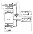
図9は、上記脈波検出装置100の機能的なブロック構成を示している。この脈波検出装置100のブロック構成は、既述のセンサユニット1と、固定台2に含まれた固定台ユニット7と、表示ユニット3とに大別されている。
表示ユニット3は、外部から操作可能に設けられて脈波検出に関する各種情報を入力するために操作される操作部24と、動脈位置検出結果や脈波測定結果などの各種情報を外部に出力するためのLED(Light Emitting Diode)やLCD(Liquid Crystal Display)などからなる表示部25とを含む。
固定台ユニット7は、この脈波検出装置100を制御するためのデータやプログラムを記憶するROM(Read Only Memory)12およびRAM(Random Access Memory)13と、この脈波検出装置100を集中的に制御するために演算を含む各種処理を実行するCPU(Central Processing Unit;中央演算処理装置)11と、加圧ポンプ15と、負圧ポンプ16と、切換弁17と、CPU11からの制御信号を受けて加圧ポンプ15,負圧ポンプ16,切換弁17を制御するための制御回路14と、特性可変フィルタ22と、A/D変換部23とを備える。
CPU11は、ROM12にアクセスしてプログラムを読出してRAM13上に展開して実行するとともに、操作部24よりユーザからの操作信号を受取り、その操作信号に基づいてこの脈波検出装置100全体の制御を行う。特に、CPU11は、操作部24から入力された操作信号に基づいて、加圧ポンプ15,負圧ポンプ16,切換弁17を制御するための制御信号を制御回路14へ送出する。また、CPU11は、脈波測定結果などを表示部25に表示させる。
加圧ポンプ15は、押圧カフ(空気袋)18の内圧(以下、「カフ圧」という)を加圧するためのポンプであり、負圧ポンプ16は、カフ圧を減圧するためのポンプである。切換弁17は、これらの加圧ポンプ15と負圧ポンプ16とのいずれかを選択的にエア管6に切換接続する。そして、制御回路14は、CPU11からの制御信号に基づいて、これらの加圧ポンプ15,負圧ポンプ16,切換弁17を制御する。
センサユニット1は、既述のセンサチップ19と、このセンサチップ19を手首上に押圧させるために加圧調整される空気袋を含む押圧カフ18とを備える。
固定台ユニット7に含まれた特性可変フィルタ22は、遮断周波数fc以上の信号成分を遮断するための低域通過フィルタである。この例では、特性可変フィルタ22は、CPU11からのフィルタ特性制御電圧によって容量が制御される可変容量ダイオードを含み、遮断周波数fcが異なる2つの特性(それぞれ「特性A」、「特性B」と呼ぶ。)をとり得る。
詳しくは、特性Aは、遮断周波数fcが、複数の圧力センサ素子41,41,…をスキャンする際の切替周波数fx(この例では20kHzとする。)以上の値fcAに設定された状態である。特性Bは、遮断周波数fcが、1個の圧力センサ素子からの圧力信号のサンプリング周波数fsの1/2よりも低い値fcBに設定された状態である。例えば、40チャネルの圧力センサ素子41,41,…からの圧力信号Ps1,Ps2,…,Ps40をスキャンする際の切替周波数fxを20kHzとすると、1個の圧力センサ素子からの圧力信号のサンプリング周波数fsは、500Hzとなる。その場合、例えばfcA=250kHzとして設定される。また、fcBは、30Hz<fcB<250Hz(=fs/2)の範囲内で、例えばfcB=100Hzとして設定される。
A/D変換部23は、センサチップ19から導出されたアナログ信号である圧力信号をデジタル情報に変換して、CPU11に与える。この結果、CPU11は、センサチップ19に含まれた複数の圧力センサ素子41,41,…が出力する圧力信号Ps1,Ps2,…を、マルチプレクサ20を介して時分割で取得することができる。
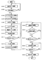
図10は、上記脈波検出装置100による測定処理のフローを示している。このフローに示される測定処理は、CPU11が、ROM22にアクセスしてプログラムを読出してRAM23上に展開して実行することによって実現される。
始めに、電源スイッチ(図示せず)がONされると、CPU11は、制御回路14に対して負圧ポンプ16を駆動するように指示し、制御回路14はこの指示に基づいて切換弁17を負圧ポンプ16側に切換えて、負圧ポンプ16を駆動する(S101)。負圧ポンプ16が駆動されることで、切換弁17を介してカフ圧が大気圧よりも十分に低くするように作用され、センサユニット1からセンサチップ19が不用意に突出して誤動作や故障するのを回避できる。
その後、センサユニット1が被測定部位90に移動される、あるいは操作部24に含まれる測定開始スイッチ(図示せず)が押される、などを検知して、測定の開始を判断する(S103)。前者の場合、筐体1Mはセンサユニット1の移動を検知するための図示されないマイクロスイッチなどを備え、CPU11は該マイクロスイッチの検出信号に基づいてセンサユニット1が移動したか否かを判定する。
測定の開始を判断すると(S103でYES)、CPU11は、圧力センサ素子41,41,…からの圧力信号を得るために、マルチプレクサ20を動作させてチャネルスキャンを開始する(S105)。これをマルチスキャンモードと呼ぶ。そして、このマルチスキャンモードでは、CPU11は、フィルタ特性制御信号によって、特性可変フィルタ22を特性Aに切り替えて、その遮断周波数をfcAとする(S107)。このfcAは複数の圧力センサ素子41,41,…からの圧力信号の切替周波数fx以上の値であるから、波形の復元に際してなまりが生じるのを防止できる。
次に、CPU11は制御回路14に対し、加圧ポンプ15を駆動させるよう制御信号を送出する。制御回路14は、この制御信号に基づいて切換弁17を加圧ポンプ15側に切換えて、加圧ポンプ15を駆動する(S109)。これにより、カフ圧が上昇して、センサユニット1のセンサチップ19が被験者の被測定部位90の表面に押圧される。
このとき、図11および図12中に示したように、センサチップ19の長手方向、すなわち、圧力センサアレイ40の延在方向が、動脈91に対して交差して配置される。
センサチップ19が被測定部位90に押圧されると、センサチップ19に含まれた圧力センサ素子41,41,…からの圧力信号がマルチプレクサ20において時分割され、ローパスフィルタ42を通して、アンプ21において増幅される。その後、増幅された圧力信号は特性可変フィルタ22に入力される。そして、特性可変フィルタ22において濾波された圧力信号は、A/D変換部23に送出される。そして、A/D変換部23でデジタル情報に変換されて、CPU11に入力される。CPU11は、これらのデジタル情報を用いてトノグラム(圧力信号の交流成分(脈波信号)の振幅を表すヒストグラム)を作成し、表示部25に表示する(図10のS111)。
例えば図13(A)は、40チャネルの圧力信号Ps1,Ps2,…,Ps40の波形を示している。なお、図13(A)では、理解の容易のために、圧力信号Ps1,Ps2,…,Ps40の波形は、縦方向に少しずつずらして描かれている。トノグラムは、図13(B)に示すように、それらの圧力信号Ps1,Ps2,…,Ps40の交流成分(脈波信号)の振幅(脈波振幅)を表すヒストグラムとして得られる。なお、図13(B)の縦軸は、各圧力信号Ps1,Ps2,…,Ps40に対応するチャネル番号を表している。
次に、CPU11は、図10のステップS111で作成したトノグラムに基づいて、複数の圧力センサ素子41,41,…のうち脈波振幅の最大値を示す圧力センサ素子(13(B)の例ではチャネル8)を動脈91上に位置するものとして検出する。そして、その動脈91上に位置する圧力センサ素子を最適チャネルとして選択するための処理を実行する(S113)。なお、最適チャネルを選択する処理については、特開2004-222847号公報に記載の公知技術などを用いることができる。この例では、最適チャネルとして、一つの圧力センサ素子(Diとする。)が選択されることとする(なお、二つ以上の最適チャネルが採用されることとしてもよい。)。
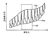
同時に、CPU11は、押圧カフ18の最適押圧力を決定するために、各圧力センサ素子41,41,…から入力される圧力信号から、その直流成分を抽出する(S115)。例えば図14に示すように、圧力信号Psは、直流成分Pdcと、交流成分(脈波信号)Pacとを含んでいる。
直流成分Pdcは、圧力信号の一定時間の平均値、または圧力信号の低域通過フィルタを通過した成分(脈波除去した成分)、または脈波立上り点(脈波成分が混入する直前)の圧力信号レベルにより求められる。
より具体的には、図10のステップS115において、圧力信号の出力変化を一定時間ごとのウィンドウ(区間)に分割し、各ウィンドウ内の平均を算出することで、直流成分Pdcを抽出することができる。あるいは、各ウィンドウ内の最大値と最小値との中間値を算出する、低域通過フィルタを用いて所定の周波数以下の値を抽出する、などを行っても、同様に直流成分Pdcを抽出することができる。なお、上述の一定時間は、被験者の脈拍に拠らない予め脈波検出装置100に設定されている時間間隔であって、一般的な一脈拍時間が含まれる1.5秒程度であることが好ましい。
次に、CPU11は、各圧力センサ素子41,41,…から入力される圧力信号に基づいて、ステップS115において抽出した直流成分Pdcが安定している箇所を検出する(S117)。直流成分Pdcが安定している箇所が検出されない場合には(S117でNO)、加圧ポンプ15による押圧カフ18に対する加圧を継続しながら、直流成分Pdcが安定している箇所が検出されるまで、上述のステップS111~S117の処理を繰り返す。
そして、CPU11は、最適チャネルの選択が完了し、直流成分Pdcが安定している箇所を検出すると(S117でYES)、マルチプレクサ20に対し最適チャネルとして決定した圧力センサ素子Diからの圧力信号を選択して送出させるようにチャネルを固定する(S119)。これをチャネル固定モードと呼ぶ。このチャネル固定モードでは、CPU11は、フィルタ特性制御信号によって、特性可変フィルタ22を特性Bに切り替えて、その遮断周波数をfcB(例えばfcB=100Hz)にする(S121)。このfcBは1個の圧力センサ素子からの圧力信号のサンプリング周波数fsの1/2よりも低い値であるから、エイリアシングノイズ(すなわち、サンプリング定理により、アナログ信号をデジタル信号に変換する場合、サンプリング周波数の1/2以上の周波数成分を持つノイズが、折り返し現象により、サンプリング周波数の1/2以下の領域に出現してしまうもの)を除去することができる。このエイリアシングノイズを除去する技術は、例えば特開2005-341994号公報に記載されている。
続いて、ステップS117で検出された直流成分Pdcが安定している箇所を一旦押圧カフ18の最適押圧力とし、押圧カフ18の圧力を調整するよう、制御回路14に対し制御信号を送出する(S123)。例えば図14の例では、枠APの範囲内に最適押圧力が得られる。
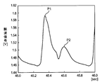
この後、CPU11は、押圧カフ18の押圧力が最適押圧に保たれた状態で最適チャネルとして選択された圧力センサ素子Diから出力された圧力信号、すなわち図15に例示するような波形データの立上がり点の先鋭度(MSP)が適切であるか否か(S125)、さらに、波形歪みがあるか否か(S127)を判定する。なお、図15では、P1が駆出波のピーク、P2が反射波のピークをそれぞれ示している。
波形データの立上がり点の先鋭度(MSP)が不適切である場合(図10のS125でNO)、あるいは波形歪みが検出される場合(S127でNO)には、波形データの立上がり点の先鋭度が適切になるまで、あるいは波形歪みが検出されなくなるまで、ステップS123の押圧力の調整を繰り返す。
そして、波形データの立上がり点の先鋭度(MSP)が適切であり(S125でYES)、かつ波形歪みが検出されない場合(S127でYES)には、CPU11は、マルチプレクサ20、アンプ21、特性可変フィルタ22およびA/D変換部23を介して、その時点の波形データを取得する(S129)。
この後、CPU11は、取得した波形データより脈波を検出し、脈波検出終了の所定条件の成立を判定する(S131)。ステップS131で脈波検出を終了するための条件は、予め設定された所定時間(例えば30秒)の経過であってもよいし、ユーザからの終了(あるいは中断)指示などであってもよい。すなわち、所定条件が成立するまで、上述のステップS129の脈波データの転送処理が繰り返される。
そして、脈波検出終了の所定条件が成立したときは(S131でYES)、CPU11は切換弁17を介して負圧ポンプ16を駆動するよう、制御回路14に対し制御信号を送出する(S133)。これにより、被測定部位90に対するセンサチップ19の押圧状態は解かれて、一連の脈波測定処理は終了する。
このようにして脈波測定が行われる場合、図11に示す圧力センサアレイ40の延在方向に対して垂直な断面(動脈91に沿った断面)では、センサチップ19の圧力センサアレイ40の両側に相当する領域10A,10Bは電極端子が存在しない平坦面になっていることから、被測定部位90に対して押圧される保護シート60の外面60aも平坦面になっている。したがって、動脈91の血管壁の外向き部分91aを平坦化するのに障害が存在しない。この結果、動脈91の血管壁の外向き部分91aを精度良く平坦化できる。したがって、血管壁の影響を受けず、動脈91の内圧の変化を正確に求めることができる。
なお、図12に示す圧力センサアレイ40の延在方向に沿った断面(動脈91を横切る断面)では、センサチップ19の圧力センサアレイ40の端部に対向する領域に電極端子アレイ50A,50Bが存在し、センサチップ19の両端近傍でフィル樹脂35等が外(被測定部位90)へ向かって凸状に盛り上がっている。しかし、この電極端子アレイ50A,50Bやフィル樹脂35等は、動脈91から外れた領域に存在するので、動脈91の血管壁の外向き部分91aを平坦化するのに障害にはならない。
また、図11に示したように、センサチップ19のシリコン基板10上で圧力センサアレイ40の両側に相当する領域10A,10Bには、電極端子アレイが存在しないので、圧力センサアレイ40の両側に相当する領域10A,10Bの寸法を小さくすることができる。その場合、例えばローパスフィルタ42とアンプ21をチップ外に設けて、センサチップ19内の処理回路を簡素化してもよい。この結果、被測定部位90に対する圧迫力を小さくでき、したがって被測定者に対する苦痛を低減できる。
この実施形態では、センサチップ19をなす基板としてシリコン基板10を用いたが、これに限られるものではない。上記基板は、MEMS技術によって圧力センサ(歪みセンサ)アレイが形成され得るものであればよく、他の材料の基板であってもよい。
また、この実施形態では、配線基板としてセラミック基板30とフレキシブル配線板31とを用いたが、これに限られるものではない。上記配線基板は、上記基板を支持し得るとともに、上記基板上の電極端子と接続される配線が設けられたものであればよく、他の材料の基板であってもよい。例えば、フレキシブル配線板31の一部を剛に構成し、その剛の部分に直接センサチップ19を搭載してもよい。
また、この実施形態では、センサチップ19を覆うように保護シート60を設けたが、これに限られるものではない。金ワイヤ32とともにセンサチップ19の表面を樹脂で実質的に平坦にコーティングして封止し、保護してもよい。
また、この実施形態では、電極端子アレイ50A,50Bが含む電極端子は、それぞれY方向に沿って1列に並ぶものとしたが、これに限られるものではない。電極端子アレイ50A,50Bは、圧力センサアレイ40の端部に対向する領域に設けられていればよい。例えば、電極端子アレイ50A,50Bは、それぞれY方向に沿って2列で、互いに1/2ピッチずつずれた配列(いわゆる千鳥状の配列)になっていてもよい。そのようにした場合、1列の場合に比して、センサチップ19のY方向寸法を縮小できる。
上述の実施形態は例示に過ぎず、この発明の範囲から逸脱することなく種々の変形が可能である。上述した複数の実施の形態は、それぞれ単独で成立し得るものであるが、実施の形態同士の組みあわせも可能である。また、異なる実施の形態の中の種々の特徴も、それぞれ単独で成立し得るものであるが、異なる実施の形態の中の特徴同士の組みあわせも可能である。
1 センサユニット
1M 筐体
2 固定台
8 ベルト
9 スライド溝
18 押圧カフ
19 センサチップ
20,20A,20B マルチプレクサ
21 アンプ
22 特性可変フィルタ
40 圧力センサアレイ
41 圧力センサ素子
42 ローパスフィルタ
50A,50B 電極端子アレイ
E1,E2,…,E28 電極端子
1M 筐体
2 固定台
8 ベルト
9 スライド溝
18 押圧カフ
19 センサチップ
20,20A,20B マルチプレクサ
21 アンプ
22 特性可変フィルタ
40 圧力センサアレイ
41 圧力センサ素子
42 ローパスフィルタ
50A,50B 電極端子アレイ
E1,E2,…,E28 電極端子
Claims (6)
- 圧力センサアレイが形成されたセンサチップを動脈が通る被測定部位に押しつけて、非観血式に脈波を検出する脈波検出装置であって、
上記センサチップは、
一方向に細長く延在する形状をもち、上記動脈に対して交差して配置される基板と、
この基板に形成された、上記一方向に沿って並ぶ複数の圧力センサ素子からなる圧力センサアレイと、
上記基板上で上記圧力センサアレイの端部に対向する領域に形成された、上記複数の圧力センサ素子の出力をチップ外へ取り出すための電極端子アレイとを備え、
上記基板上で上記圧力センサアレイの両側に相当する領域は、電極端子が存在しない平坦面になっていることを特徴とする脈波検出装置。 - 請求項1に記載の脈波検出装置において、
上記電極端子アレイは、上記一方向に対して垂直な方向に沿って並ぶ複数の電極端子を含むことを特徴とする脈波検出装置。 - 請求項1または2に記載の脈波検出装置において、
上記基板の上記圧力センサアレイの両側に相当する領域に、上記圧力センサアレイの上記圧力センサ素子の出力を処理して、上記電極端子アレイの電極端子へ送出する処理回路が一体に形成されていることを特徴とする脈波検出装置。 - 請求項3に記載の脈波検出装置において、
上記処理回路は、上記圧力センサアレイの上記複数の圧力センサ素子の出力を選択して、低減された数の圧力センサ素子の出力を時分割で取り出すマルチプレクサを含むことを特徴とする脈波検出装置。 - 請求項1から4までのいずれか一つに記載の脈波検出装置において、
上記センサチップを搭載して支持する配線基板を備え、
上記センサチップの上記電極端子アレイの電極端子は、上記配線基板上の対応する電極パッドに、ワイヤを介して接続されていることを特徴とする脈波検出装置。 - 請求項5に記載の脈波検出装置において、
上記ワイヤは樹脂で封止されていることを特徴とする脈波検出装置。
Priority Applications (3)
| Application Number | Priority Date | Filing Date | Title |
|---|---|---|---|
| EP15743885.4A EP3100676B1 (en) | 2014-01-31 | 2015-01-19 | Pulse wave detector |
| CN201580003402.XA CN105848572A (zh) | 2014-01-31 | 2015-01-19 | 脉搏波检测装置 |
| US15/199,154 US10251572B2 (en) | 2014-01-31 | 2016-06-30 | Pulse wave detection apparatus |
Applications Claiming Priority (2)
| Application Number | Priority Date | Filing Date | Title |
|---|---|---|---|
| JP2014-017727 | 2014-01-31 | ||
| JP2014017727A JP6256058B2 (ja) | 2014-01-31 | 2014-01-31 | 脈波検出装置 |
Related Child Applications (1)
| Application Number | Title | Priority Date | Filing Date |
|---|---|---|---|
| US15/199,154 Continuation US10251572B2 (en) | 2014-01-31 | 2016-06-30 | Pulse wave detection apparatus |
Publications (1)
| Publication Number | Publication Date |
|---|---|
| WO2015115236A1 true WO2015115236A1 (ja) | 2015-08-06 |
Family
ID=53756813
Family Applications (1)
| Application Number | Title | Priority Date | Filing Date |
|---|---|---|---|
| PCT/JP2015/051273 Ceased WO2015115236A1 (ja) | 2014-01-31 | 2015-01-19 | 脈波検出装置 |
Country Status (5)
| Country | Link |
|---|---|
| US (1) | US10251572B2 (ja) |
| EP (1) | EP3100676B1 (ja) |
| JP (1) | JP6256058B2 (ja) |
| CN (1) | CN105848572A (ja) |
| WO (1) | WO2015115236A1 (ja) |
Cited By (3)
| Publication number | Priority date | Publication date | Assignee | Title |
|---|---|---|---|---|
| JP2015144628A (ja) * | 2014-01-31 | 2015-08-13 | オムロンヘルスケア株式会社 | 脈波検出装置 |
| JP2017196309A (ja) * | 2016-04-28 | 2017-11-02 | オムロンヘルスケア株式会社 | 圧脈波センサ、脈波検出装置、及び、生体情報測定装置 |
| CN107920755A (zh) * | 2015-08-24 | 2018-04-17 | 欧姆龙健康医疗事业株式会社 | 脉搏波测定装置 |
Families Citing this family (10)
| Publication number | Priority date | Publication date | Assignee | Title |
|---|---|---|---|---|
| JP2967290B2 (ja) | 1990-07-11 | 1999-10-25 | 富士ゼロックス株式会社 | 用紙搬送装置 |
| US9772222B2 (en) * | 2014-12-08 | 2017-09-26 | Samsung Electronics Co., Ltd. | Retainer for photoelectric sensor and photoelectric pulse wave measuring apparatus including the same |
| JP6528602B2 (ja) * | 2015-08-24 | 2019-06-12 | オムロンヘルスケア株式会社 | 圧脈波センサ及び生体情報測定装置 |
| JP6540397B2 (ja) * | 2015-09-07 | 2019-07-10 | オムロンヘルスケア株式会社 | 圧脈波センサの検査方法及び圧脈波センサの製造方法 |
| JP6766710B2 (ja) * | 2017-03-15 | 2020-10-14 | オムロンヘルスケア株式会社 | 血圧測定装置、方法及びプログラム |
| WO2019010423A1 (en) * | 2017-07-07 | 2019-01-10 | The Texas A&M University System | SYSTEM AND METHOD FOR MONITORING SLEEP-FREE ARTERIAL PRESSURE |
| JP7091831B2 (ja) * | 2018-05-24 | 2022-06-28 | オムロンヘルスケア株式会社 | センサモジュール、センサモジュールの製造方法、及び血圧測定装置 |
| CN112690766B (zh) * | 2020-12-29 | 2022-10-11 | 上海掌门科技有限公司 | 一种利用诊脉设备测量用户脉搏信息的方法与设备 |
| CN112690765B (zh) * | 2020-12-29 | 2023-05-19 | 上海掌门科技有限公司 | 一种利用诊脉设备测量用户脉搏信息的方法与设备 |
| CN117122297B (zh) * | 2023-08-15 | 2025-12-16 | 深圳市安博健康科技有限公司 | 一种张力法压力脉搏波测量装置及方法 |
Citations (7)
| Publication number | Priority date | Publication date | Assignee | Title |
|---|---|---|---|---|
| JPS63294832A (ja) * | 1988-01-28 | 1988-12-01 | Koorin Denshi Kk | 脈波検出装置 |
| JP2577984B2 (ja) * | 1987-01-27 | 1997-02-05 | エス・アール・アイ・インターナシヨナル | 血圧測定装置 |
| JP2004222847A (ja) | 2003-01-21 | 2004-08-12 | Omron Healthcare Co Ltd | 脈波検出装置および方法 |
| JP2005341994A (ja) | 2004-05-31 | 2005-12-15 | Omron Healthcare Co Ltd | 脈波検出装置および脈波検出方法 |
| JP2006020823A (ja) * | 2004-07-08 | 2006-01-26 | Omron Healthcare Co Ltd | アレイ型静電容量式圧脈波センサおよびこれを備えた脈波測定装置 |
| KR20090011479A (ko) * | 2007-07-26 | 2009-02-02 | 삼성전자주식회사 | 혈압측정장치 |
| JP2011239840A (ja) | 2010-05-14 | 2011-12-01 | Olympus Corp | 血圧測定システム |
Family Cites Families (10)
| Publication number | Priority date | Publication date | Assignee | Title |
|---|---|---|---|---|
| US4947855A (en) * | 1989-02-20 | 1990-08-14 | Colin Electronics Co., Ltd. | Blood pressure measuring apparatus |
| JP2798764B2 (ja) * | 1990-01-09 | 1998-09-17 | コーリン電子株式会社 | 半導体圧脈波センサ |
| US5179956A (en) * | 1990-07-06 | 1993-01-19 | Colin Electronics Co., Ltd. | Contact pressure sensor |
| US7104375B2 (en) * | 2003-07-31 | 2006-09-12 | Motoczysz Llc | Vehicle with separate gearbox clutch and back-torque-limiting slipper clutch |
| US8245724B2 (en) * | 2007-07-06 | 2012-08-21 | Wfk & Associates, Llc | Pneumatic system for residential use |
| JP5188289B2 (ja) * | 2008-06-26 | 2013-04-24 | ラピスセミコンダクタ株式会社 | プリント基板の製造方法 |
| JP5487963B2 (ja) * | 2009-12-29 | 2014-05-14 | オムロンヘルスケア株式会社 | 血圧情報測定装置用カフおよびこれを備えた血圧情報測定装置 |
| KR20110123651A (ko) * | 2010-05-07 | 2011-11-15 | 한국전자통신연구원 | 생략 부호화를 이용한 영상 부호화 및 복호화 장치 및 그 방법 |
| US9596988B2 (en) * | 2011-10-12 | 2017-03-21 | Purdue Research Foundation | Pressure sensors for small-scale applications and related methods |
| JP6256058B2 (ja) * | 2014-01-31 | 2018-01-10 | オムロンヘルスケア株式会社 | 脈波検出装置 |
-
2014
- 2014-01-31 JP JP2014017727A patent/JP6256058B2/ja active Active
-
2015
- 2015-01-19 WO PCT/JP2015/051273 patent/WO2015115236A1/ja not_active Ceased
- 2015-01-19 EP EP15743885.4A patent/EP3100676B1/en active Active
- 2015-01-19 CN CN201580003402.XA patent/CN105848572A/zh active Pending
-
2016
- 2016-06-30 US US15/199,154 patent/US10251572B2/en active Active
Patent Citations (7)
| Publication number | Priority date | Publication date | Assignee | Title |
|---|---|---|---|---|
| JP2577984B2 (ja) * | 1987-01-27 | 1997-02-05 | エス・アール・アイ・インターナシヨナル | 血圧測定装置 |
| JPS63294832A (ja) * | 1988-01-28 | 1988-12-01 | Koorin Denshi Kk | 脈波検出装置 |
| JP2004222847A (ja) | 2003-01-21 | 2004-08-12 | Omron Healthcare Co Ltd | 脈波検出装置および方法 |
| JP2005341994A (ja) | 2004-05-31 | 2005-12-15 | Omron Healthcare Co Ltd | 脈波検出装置および脈波検出方法 |
| JP2006020823A (ja) * | 2004-07-08 | 2006-01-26 | Omron Healthcare Co Ltd | アレイ型静電容量式圧脈波センサおよびこれを備えた脈波測定装置 |
| KR20090011479A (ko) * | 2007-07-26 | 2009-02-02 | 삼성전자주식회사 | 혈압측정장치 |
| JP2011239840A (ja) | 2010-05-14 | 2011-12-01 | Olympus Corp | 血圧測定システム |
Cited By (6)
| Publication number | Priority date | Publication date | Assignee | Title |
|---|---|---|---|---|
| JP2015144628A (ja) * | 2014-01-31 | 2015-08-13 | オムロンヘルスケア株式会社 | 脈波検出装置 |
| CN107920755A (zh) * | 2015-08-24 | 2018-04-17 | 欧姆龙健康医疗事业株式会社 | 脉搏波测定装置 |
| JP2017196309A (ja) * | 2016-04-28 | 2017-11-02 | オムロンヘルスケア株式会社 | 圧脈波センサ、脈波検出装置、及び、生体情報測定装置 |
| CN109069027A (zh) * | 2016-04-28 | 2018-12-21 | 欧姆龙健康医疗事业株式会社 | 压力脉搏波传感器、脉搏波检测装置和生物信息测定装置 |
| EP3453320A4 (en) * | 2016-04-28 | 2020-01-22 | Omron Healthcare Co., Ltd. | PRESSURE PULSE SHAFT SENSOR, PULSE SHAFT DETECTION DEVICE AND DEVICE FOR MEASURING BIOLOGICAL INFORMATION |
| CN109069027B (zh) * | 2016-04-28 | 2021-09-10 | 欧姆龙健康医疗事业株式会社 | 脉搏波检测装置和生物信息测定装置 |
Also Published As
| Publication number | Publication date |
|---|---|
| CN105848572A (zh) | 2016-08-10 |
| EP3100676A1 (en) | 2016-12-07 |
| US10251572B2 (en) | 2019-04-09 |
| JP6256058B2 (ja) | 2018-01-10 |
| EP3100676B1 (en) | 2020-09-30 |
| EP3100676A4 (en) | 2017-09-27 |
| JP2015144628A (ja) | 2015-08-13 |
| US20160310021A1 (en) | 2016-10-27 |
Similar Documents
| Publication | Publication Date | Title |
|---|---|---|
| JP6256058B2 (ja) | 脈波検出装置 | |
| US10973419B2 (en) | Intravascular pressure devices incorporating sensors manufactured using deep reactive ion etching | |
| KR101366809B1 (ko) | 혈압측정장치 및 혈압측정방법 | |
| US20100148286A1 (en) | Contact-force sensor package and method of fabricating the same | |
| JP6991022B2 (ja) | 表示制御装置およびプログラム | |
| JP4487639B2 (ja) | 脈波検出装置および脈波検出方法 | |
| WO2018123275A1 (ja) | 血圧計および血圧測定方法並びに機器 | |
| TW202114591A (zh) | 脈搏量測設備 | |
| KR101345381B1 (ko) | 혈압측정장치 | |
| JP2019051128A (ja) | 電極ユニット、脈波測定ユニット、および脈波測定装置 | |
| JP7166120B2 (ja) | 脈波センサ及び脈波測定方法 | |
| WO2016147503A1 (ja) | Mems圧力センサとその位置決め方法 | |
| CN113950284A (zh) | 用于监测子宫收缩的设备 | |
| WO2017043384A1 (ja) | 圧脈波センサの検査方法及び圧脈波センサの製造方法 | |
| JP6894330B2 (ja) | 健康機器用流路形成部材、健康機器用流路形成ユニット、および健康機器 | |
| JP6773007B2 (ja) | 静電容量式圧力センサ | |
| JPH0992670A (ja) | センサ装置の構造およびその構造を実現するための実装方法 | |
| JP6543584B2 (ja) | 超音波探触子の製造方法および超音波診断装置 | |
| JP6637701B2 (ja) | 圧力計、圧力計測装置、及び血圧計 | |
| JP2019051010A5 (ja) | ||
| TW202432051A (zh) | 生理訊號量測設備 | |
| WO2017033730A1 (ja) | 圧脈波センサ及び生体情報測定装置 | |
| KR102182598B1 (ko) | 맥박 센싱 모듈, 혈압 산출 모듈, 혈압 측정 장치 및 맥박 센싱 모듈의 제조 방법 | |
| US20260108161A1 (en) | Flexible dual-modality system and method for continuous blood pressure monitoring | |
| JPH0434808Y2 (ja) |
Legal Events
| Date | Code | Title | Description |
|---|---|---|---|
| 121 | Ep: the epo has been informed by wipo that ep was designated in this application |
Ref document number: 15743885 Country of ref document: EP Kind code of ref document: A1 |
|
| DPE1 | Request for preliminary examination filed after expiration of 19th month from priority date (pct application filed from 20040101) | ||
| REEP | Request for entry into the european phase |
Ref document number: 2015743885 Country of ref document: EP |
|
| WWE | Wipo information: entry into national phase |
Ref document number: 2015743885 Country of ref document: EP |
|
| NENP | Non-entry into the national phase |
Ref country code: DE |