WO2015118901A1 - コンデンサ - Google Patents
コンデンサ Download PDFInfo
- Publication number
- WO2015118901A1 WO2015118901A1 PCT/JP2015/050524 JP2015050524W WO2015118901A1 WO 2015118901 A1 WO2015118901 A1 WO 2015118901A1 JP 2015050524 W JP2015050524 W JP 2015050524W WO 2015118901 A1 WO2015118901 A1 WO 2015118901A1
- Authority
- WO
- WIPO (PCT)
- Prior art keywords
- porous metal
- metal substrate
- low porosity
- capacitor
- terminal electrode
- Prior art date
- Legal status (The legal status is an assumption and is not a legal conclusion. Google has not performed a legal analysis and makes no representation as to the accuracy of the status listed.)
- Ceased
Links
Images



Classifications
-
- H—ELECTRICITY
- H01—ELECTRIC ELEMENTS
- H01G—CAPACITORS; CAPACITORS, RECTIFIERS, DETECTORS, SWITCHING DEVICES, LIGHT-SENSITIVE OR TEMPERATURE-SENSITIVE DEVICES OF THE ELECTROLYTIC TYPE
- H01G9/00—Electrolytic capacitors, rectifiers, detectors, switching devices, light-sensitive or temperature-sensitive devices; Processes of their manufacture
- H01G9/0029—Processes of manufacture
- H01G9/0032—Processes of manufacture formation of the dielectric layer
-
- H—ELECTRICITY
- H01—ELECTRIC ELEMENTS
- H01G—CAPACITORS; CAPACITORS, RECTIFIERS, DETECTORS, SWITCHING DEVICES, LIGHT-SENSITIVE OR TEMPERATURE-SENSITIVE DEVICES OF THE ELECTROLYTIC TYPE
- H01G9/00—Electrolytic capacitors, rectifiers, detectors, switching devices, light-sensitive or temperature-sensitive devices; Processes of their manufacture
- H01G9/004—Details
- H01G9/008—Terminals
- H01G9/012—Terminals specially adapted for solid capacitors
-
- H—ELECTRICITY
- H01—ELECTRIC ELEMENTS
- H01G—CAPACITORS; CAPACITORS, RECTIFIERS, DETECTORS, SWITCHING DEVICES, LIGHT-SENSITIVE OR TEMPERATURE-SENSITIVE DEVICES OF THE ELECTROLYTIC TYPE
- H01G9/00—Electrolytic capacitors, rectifiers, detectors, switching devices, light-sensitive or temperature-sensitive devices; Processes of their manufacture
- H01G9/004—Details
- H01G9/04—Electrodes or formation of dielectric layers thereon
-
- H—ELECTRICITY
- H01—ELECTRIC ELEMENTS
- H01G—CAPACITORS; CAPACITORS, RECTIFIERS, DETECTORS, SWITCHING DEVICES, LIGHT-SENSITIVE OR TEMPERATURE-SENSITIVE DEVICES OF THE ELECTROLYTIC TYPE
- H01G9/00—Electrolytic capacitors, rectifiers, detectors, switching devices, light-sensitive or temperature-sensitive devices; Processes of their manufacture
- H01G9/004—Details
- H01G9/04—Electrodes or formation of dielectric layers thereon
- H01G9/042—Electrodes or formation of dielectric layers thereon characterised by the material
- H01G9/045—Electrodes or formation of dielectric layers thereon characterised by the material based on aluminium
-
- H—ELECTRICITY
- H01—ELECTRIC ELEMENTS
- H01G—CAPACITORS; CAPACITORS, RECTIFIERS, DETECTORS, SWITCHING DEVICES, LIGHT-SENSITIVE OR TEMPERATURE-SENSITIVE DEVICES OF THE ELECTROLYTIC TYPE
- H01G9/00—Electrolytic capacitors, rectifiers, detectors, switching devices, light-sensitive or temperature-sensitive devices; Processes of their manufacture
- H01G9/004—Details
- H01G9/04—Electrodes or formation of dielectric layers thereon
- H01G9/048—Electrodes or formation of dielectric layers thereon characterised by their structure
-
- H—ELECTRICITY
- H01—ELECTRIC ELEMENTS
- H01G—CAPACITORS; CAPACITORS, RECTIFIERS, DETECTORS, SWITCHING DEVICES, LIGHT-SENSITIVE OR TEMPERATURE-SENSITIVE DEVICES OF THE ELECTROLYTIC TYPE
- H01G9/00—Electrolytic capacitors, rectifiers, detectors, switching devices, light-sensitive or temperature-sensitive devices; Processes of their manufacture
- H01G9/004—Details
- H01G9/04—Electrodes or formation of dielectric layers thereon
- H01G9/048—Electrodes or formation of dielectric layers thereon characterised by their structure
- H01G9/055—Etched foil electrodes
-
- H—ELECTRICITY
- H01—ELECTRIC ELEMENTS
- H01G—CAPACITORS; CAPACITORS, RECTIFIERS, DETECTORS, SWITCHING DEVICES, LIGHT-SENSITIVE OR TEMPERATURE-SENSITIVE DEVICES OF THE ELECTROLYTIC TYPE
- H01G9/00—Electrolytic capacitors, rectifiers, detectors, switching devices, light-sensitive or temperature-sensitive devices; Processes of their manufacture
- H01G9/004—Details
- H01G9/07—Dielectric layers
-
- H—ELECTRICITY
- H01—ELECTRIC ELEMENTS
- H01G—CAPACITORS; CAPACITORS, RECTIFIERS, DETECTORS, SWITCHING DEVICES, LIGHT-SENSITIVE OR TEMPERATURE-SENSITIVE DEVICES OF THE ELECTROLYTIC TYPE
- H01G9/00—Electrolytic capacitors, rectifiers, detectors, switching devices, light-sensitive or temperature-sensitive devices; Processes of their manufacture
- H01G9/15—Solid electrolytic capacitors
Definitions
- the present invention relates to a capacitor and a manufacturing method thereof.
- a valve metal such as niobium, tantalum, titanium, or aluminum or an alloy thereof is used as an anode, an oxide film is formed on the surface thereof as a dielectric layer, and an electrolyte layer is formed on the dielectric layer.
- an electrolyte layer is formed on the dielectric layer.
- ESR equivalent series resistance
- Patent Document 1 discloses an anode formed by molding and sintering a valve metal powder as a solid electrolytic capacitor having a small ESR and leakage current, a dielectric layer formed on the surface thereof, and a dielectric layer formed on the dielectric layer.
- a solid electrolytic capacitor including a cathode and an outer body resin covering the cathode is disclosed.
- the anode is made of a sintered body of valve metal powder such as niobium, tantalum, titanium, and aluminum. Since such a sintered body is a porous body having a high porosity, a large electrostatic capacity can be obtained, but the mechanical strength is low. Therefore, in order to ensure the strength that can be mounted on the circuit board, it has been necessary to cover with the exterior body resin as described in Patent Document 1.
- An object of the present invention is to provide a capacitor that can acquire a large capacitance, has a small leakage current, and has an excellent mechanical strength.
- the present inventors provide a capacitor having excellent mechanical strength by forming a low porosity portion in a part of a porous metal substrate having a high porosity. Found that you can.
- Preparing a porous metal substrate having a high porosity portion and a low porosity portion Preparing a porous metal substrate having a high porosity portion and a low porosity portion; Forming a dielectric layer on the porous metal substrate; Forming an upper electrode on the dielectric layer; Forming a first terminal electrode to be electrically connected to the porous metal substrate; And a step of forming a second terminal electrode so as to be electrically connected to the upper electrode.
- a capacitor having improved mechanical strength is provided by using a porous metal substrate having a high porosity portion and a low porosity portion.
- FIG. 1 is a schematic cross-sectional view of a capacitor in one embodiment of the present invention.
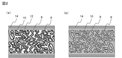
- Fig.2 (a) is an enlarged view of the high porosity part in sectional drawing shown in FIG.
- FIG.2 (b) is an enlarged view of the high porosity part in another aspect.
- FIGS. 3A to 3D are diagrams showing manufacturing steps of the capacitor of FIG. FIGS. 3-2 (e) to (h) are continuations of FIG. 3-1, and are diagrams showing a manufacturing process of the capacitor of FIG. FIGS. 3-3 (i) to (m) are continuations of FIG. 3-2 and show the manufacturing process of the capacitor of FIG. FIG.
- FIG. 4 is a schematic enlarged cross-sectional view of the second terminal electrode portion of the capacitor according to a preferred embodiment of the present invention.
- FIG. 5 is a schematic cross-sectional view of a capacitor in still another aspect of the present invention.
- 6 (a) and 6 (b) are schematic cross-sectional views of a capacitor according to still another embodiment of the present invention.
- FIG. 7 is a schematic cross-sectional view of a capacitor according to still another embodiment of the present invention.
- 8A and 8B are schematic cross-sectional views of a capacitor according to still another embodiment of the present invention.
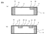
- FIGS. 9A and 9B are schematic cross-sectional views of capacitors according to still another embodiment of the present invention.
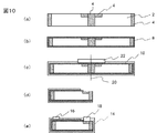
- 10 (a) to 10 (e) are diagrams showing manufacturing steps of the capacitor of FIG. 9 (a).
- the capacitor 1 of the present embodiment has a substantially rectangular parallelepiped shape. As shown schematically in FIG. 1 and FIG. 2 (a), the capacitor 1 has a high porosity portion 2 at the center portion and a side portion.
- the wiring electrode 12 is formed so as to be electrically connected to the electrode 10, and the protective film 14 is further formed thereon.
- a first terminal electrode 16 and a second terminal electrode 18 are provided on the side surface of the porous metal substrate 6 so as to face each other, and the first terminal electrode 16 is electrically connected to the porous metal substrate 6.
- the second terminal electrode 18 is electrically connected to the upper electrode 10 through the wiring electrode 12.
- the “porosity” of a porous metal substrate refers to the ratio of voids in the porous metal substrate.
- the porosity can be measured as follows.
- the porous metal substrate is processed into a thin piece having a thickness of 60 nm or less by focused ion beam (FIB) processing.
- a predetermined region (5 ⁇ m ⁇ 5 ⁇ m) of the thin sample is photographed using a transmission electron microscope (TEM).
- TEM transmission electron microscope
- the area where the metal of the porous metal substrate exists is obtained.
- the “high porosity portion” of the porous metal substrate means a region having a porosity of 25% or more.
- the “low porosity portion” of the porous metal substrate is a portion having a lower porosity than the high porosity portion, specifically, a porosity of 70% or less of the high porosity portion. Means an area.
- the “side surface” of the porous metal substrate means a surface substantially perpendicular to the mounting surface of the capacitor. 1 to 10, the lower surface is the mounting surface of the capacitor.
- the metal constituting the porous metal substrate is not particularly limited as long as it is conductive.
- examples thereof include metals such as aluminum, tantalum, nickel, copper, titanium, niobium and iron, and alloys such as stainless steel and duralumin. It is done.
- Preferred porous metal substrates are not particularly limited, and examples include aluminum etching foils, tantalum powder sintered bodies, nickel powder sintered bodies, and porous metals synthesized by a dealloying method.
- the porous metal substrate can be produced by methods well known in the art, such as etching, sintering, and dealloying methods.
- a commercially available porous metal substrate may be used as the porous metal substrate.
- the thickness of the porous metal substrate is not particularly limited and can be appropriately selected according to the purpose.
- the thickness may be 10 to 1,000 ⁇ m, preferably 30 to 300 ⁇ m.
- the thickness of the porous metal substrate means the length in the direction perpendicular to the capacitor mounting surface. By setting the thickness to 1,000 ⁇ m or less, it is advantageous in terms of miniaturization. On the other hand, when the thickness is 10 ⁇ m or more, the strength of the porous metal material can be more sufficiently secured.
- the porous metal substrate 6 has a low porosity portion 4 on a pair of side surfaces facing each other, and a high porosity portion 2 therebetween.
- the porosity of the high porosity portion of the porous metal substrate is preferably 30% or more, more preferably 35% or more, from the viewpoint of increasing the surface area and increasing the capacity of the capacitor. Moreover, from a viewpoint of ensuring mechanical strength, 80% or less is preferable and 65% or less is more preferable.
- the porosity of the low porosity portion of the porous metal substrate is preferably 60% or less of the porosity of the high porosity portion from the viewpoint of increasing the mechanical strength. More preferably, the porosity is 50% or less.
- the porosity of the low porosity portion is preferably 20% or less, and more preferably 10% or less. Further, the low porosity portion may have a porosity of 0%.
- the low porosity part is located opposite to the side part of the porous metal substrate.
- the “side surface portion” of the porous metal substrate means a region including the side surface of the porous metal substrate and extending to a certain distance from this side surface. That is, a part of the low porosity portion may constitute at least a part of the side surface of the porous metal substrate.
- part of the low porosity portion preferably constitutes at least 30% of the side surface of the porous metal substrate, and more preferably constitutes 60% or more of the region. More preferably, a part of the low porosity portion constitutes the entire region of the side surface of the porous metal substrate.
- the side surface of the porous metal substrate is composed of a low porosity portion.
- the width of the low porosity portion (the length from the side surface common to the side surface of the porous metal substrate to the surface facing the surface; in FIGS. 1 to 10, the length in the horizontal direction of the paper surface) is 3 ⁇ m to 1 mm, preferably 10 to 500 ⁇ m.
- the width of the low porosity portion is 3 ⁇ m or more, more preferably 10 ⁇ m or more, the mechanical strength of the capacitor can be increased.
- the width of the low porosity portion to 1 mm or less, it becomes possible to secure a larger high porosity portion in a porous metal member having the same volume, and to obtain a high capacitance. .
- the method for forming the low porosity portion is not particularly limited as long as a desired porosity can be obtained, but it is preferably formed by, for example, pressing with a mold or the like.
- the pressing may be performed so as to be sandwiched from the upper and lower surfaces of the porous metal substrate, or may be performed only from one surface.
- all solid-state pulse lasers such as YVO 4 laser, CO 2 laser, YAG laser, excimer laser, femtosecond laser, picosecond laser, and nanosecond laser can be used for porous metal substrates previously porous. May be used to form the low porosity portion. All-solid pulse lasers such as femtosecond lasers, picosecond lasers, and nanosecond lasers are preferred because the shape and porosity of the low porosity part can be controlled more precisely.
- the low porosity portion may be formed by filling the pores of the high porosity portion as described above, but can also be formed in the process of forming the pores in a non-porous metal substrate.
- the porous metal foil is manufactured by etching
- the portion where the low porosity portion is to be formed is masked and then etched, whereby the masking portion becomes a non-etched layer and the low porosity portion is formed.
- the etching process is stopped before the pores are formed up to the center portion of the foil. As a result, the central portion becomes a non-etched layer, and a low porosity portion is formed.
- low porosity portions having various shapes can be formed.
- a dielectric layer 8 is formed on the porous metal substrate 6.
- the material for forming the dielectric layer is not particularly limited as long as it is insulative, but preferably, AlO x (for example, Al 2 O 3 ), SiO x (for example, SiO 2 ), AlTiO x , SiTiO x , HfO.
- the thickness of the dielectric layer is not particularly limited, but is preferably 5 to 100 nm, for example, and more preferably 10 to 50 nm. By setting the thickness of the dielectric layer to 5 nm or more, it is possible to improve the insulation and to reduce the leakage current. Further, by setting the thickness of the dielectric layer to 100 nm or less, it is possible to obtain a larger capacitance.
- the dielectric layer can be formed by an atomic layer (ALD) method.
- ALD atomic layer
- an upper electrode 10 is formed on the dielectric layer 8.
- the material constituting the upper electrode is not particularly limited as long as it is conductive, but Ni, Cu, Al, W, Ti, Ag, Au, Pt, Zn, Sn, Pb, Fe, Cr, Mo, Ru, Pd , Ta and their alloy layers, such as CuNi, AuNi, AuSn, and metal nitrides such as TiN, TiAlN, TiON, TiAlON, and TaN, and TiN and TiON are preferred.
- the material constituting the upper electrode may be a conductive polymer, and examples thereof include PEDOT / PSS (poly (3,4-ethylenedioxythiophene) / polystyrene sulfonic acid), polyaniline, and polypyrrole. .
- the thickness of the upper electrode is not particularly limited, but is preferably 3 nm or more, for example, and more preferably 10 nm or more. By setting the thickness of the upper electrode to 3 nm or more, the resistance of the upper electrode itself can be reduced.
- the upper electrode can be formed by the ALD method. By using the ALD method, the capacitance of the capacitor can be increased. Alternatively, a dielectric layer can be coated to substantially fill the pores of the porous metal substrate, chemical vapor deposition (CVD), plating, bias sputtering, Sol-Gel, high conductivity
- the upper electrode may be formed by a method such as molecular filling. Alternatively, a conductive film may be formed on the dielectric layer by the ALD method, and the upper electrode may be formed by filling the pores by another method.
- the surface of the upper electrode is additionally added to the surface of the upper electrode by a method such as sputtering, vapor deposition, or plating.
- a lead electrode layer made of, for example, may be formed.
- the upper electrode 10 is formed so that the conductive material constituting the upper electrode fills the pores of the porous metal substrate 6. Also good.
- the upper electrode 10 may also serve as a wiring electrode described below.
- the pores of the porous metal substrate do not need to be substantially completely filled with the conductive material, and are filled with 50% or more, preferably 70% or more, more preferably 90% or more of the pores. It only has to be. From the viewpoint of reducing the resistance of the upper electrode, it is more preferable that the upper electrode is substantially completely filled.
- a wiring electrode 12 is formed on the upper electrode 10.
- the material which comprises a wiring electrode is not specifically limited, For example, Cu, Ni, Sn, Al, Ag, Au etc. are mentioned.
- the method for forming the wiring electrode is not particularly limited, and for example, CVD, plating, sputtering, or the like can be used.
- the porous metal substrate on which the dielectric layer 8, the upper electrode 10, and the wiring electrode 12 are formed is protected by a protective layer 14.
- the protective layer 14 is formed so as to cover the entire porous metal substrate except for the connection portion with the terminal electrode.
- the protective layer can further increase the moisture resistance, insulation, and mechanical strength of the capacitor.
- the material constituting the protective layer is not particularly limited as long as it is insulating.
- the same material as that for forming the dielectric layer preferably SiN x , SiO x , AlTiO x , AlO x , more preferably SiO x , or a resin coat such as polyepoxy or polyimide, a glass coat, or the like can be used.
- the thickness of the protective layer is not particularly limited as long as it has a desired function, for example, moisture resistance or insulation, but it is preferably 0.5 ⁇ m to 50 ⁇ m, preferably 1 ⁇ m to 20 ⁇ m.
- the method for forming the protective layer is not particularly limited, and can be appropriately selected according to the material such as CVD, plating, sputtering, spraying, screen printing, dispenser, resin film lamination, and the like.
- the capacitor 1 has a pair of opposing first terminal electrode 16 and second terminal electrode 18 on the side surface.
- the first terminal electrode 16 is electrically connected to the porous metal substrate 6, the second terminal electrode 18 is electrically connected to the upper electrode 10, and the first terminal electrode and the second terminal electrode are in the capacitor. Installed to be electrically isolated.
- terminal electrode The material constituting the first terminal electrode and the second terminal electrode (hereinafter collectively referred to as “terminal electrode”) is not particularly limited as long as it is conductive.
- terminal electrode Cu, Ni, Sn, Au, Ag, Pb
- Such metals and alloys thereof can be used.
- the thickness of the terminal electrode is not particularly limited, but may be 1 to 50 ⁇ m, preferably 1 to 20 ⁇ m.
- the method for forming the terminal electrode is not particularly limited.
- the terminal electrode may be formed by plating, or may be formed by applying and baking a conductive paste.
- the porous metal base material has a low porosity portion with high mechanical strength, for example, stress applied when mounting on a substrate such as a glass epoxy substrate, a ceramic substrate, a resin substrate, In particular, it has high durability against bending stress.
- the low porosity portion has high mechanical strength, deformation of the porous metal substrate during manufacturing can be suppressed.
- the ALD method as described above enables formation of a thin film having high insulating properties, but the obtained dielectric film has low interface strength (or adhesion) with the porous metal base material, and is caused by stress. Prone to peeling, delamination and cracks. Since the capacitor of the present invention has high mechanical strength, it is possible to suppress the peeling of the dielectric film, the delamination, and the generation of cracks due to the deformation of the element.
- the capacitor of the present invention can have a ratio of length to thickness of 3 or more, preferably 4 or more.
- FIG. 3-1, FIG. 3-2 and FIG. 3-3 are collectively referred to as FIG.
- a porous metal substrate 6 is prepared.
- the porous metal substrate can be produced by methods well known in the art, such as etching, sintering, and dealloying methods.
- a commercially available porous metal substrate may be used as the porous metal substrate.
- the low porosity portion 4 is formed in the porous metal substrate 6.
- a plurality of low porosity portions are formed on one porous metal substrate at intervals according to the size of a desired capacitor. That is, a plurality of elements are formed from this porous metal substrate.
- the low porosity portion is formed, for example, on a press using a die or the like by a CO 2 laser, a YAG laser, an excimer laser, and an all solid-state pulse laser such as a femtosecond laser, a picosecond laser, and a nanosecond laser be able to.
- the porous metal substrate is cut along the broken line 20 at the low porosity portion (preferably at the substantially central portion). However, at this time, the porous metal substrate is not completely cut into element units, and one side surface is maintained in a state of being connected to an adjacent element.
- the method for cutting the porous metal substrate is not particularly limited, but can be cut by, for example, laser cutting, die cutting, dicer, carbide blade, slitter, cutting with a pinnacle blade, alone or in combination, etc. .
- the production of the capacitor of the present invention includes a step of cutting the porous metal substrate as described above.
- the presence of a porous portion causes the occurrence of sagging such as burrs and / or stretching / deformation of the cut surface in the cutting direction during the cutting.
- the cut portion is a low porosity portion, it is possible to suppress the occurrence of such burrs.
- a dielectric layer 8 is formed on the surface of the porous metal substrate 6 (in the illustrated example, over the entire exposed surface of the porous metal substrate). As described above, the dielectric layer is formed by the ALD method.
- a mask 22 is formed on a part of the porous metal base material on which the dielectric layer 8 is formed, specifically, at a location where the first terminal electrode 16 is formed later. .
- the material constituting the mask is not particularly limited, and examples thereof include an epoxy resin, a polyimide resin, and a silicone resin.
- the method for forming the mask is not particularly limited, and examples thereof include screen printing, dispenser, dip, ink jet, and spray.
- the upper electrode 10 is formed on the dielectric layer 8.
- a conductive material layer serving as an upper electrode is formed so as to cover the entire element, and the upper electrode also serves as a wiring electrode.
- the upper electrode can be formed by methods such as ALD, CVD, plating, bias sputtering, Sol-Gel, and conductive polymer filling. Moreover, these methods can be used in combination. For example, a conductive film may be formed on the dielectric layer by the ALD method, and the upper electrode may be formed by filling the pores by another method.
- the porous metal substrate is cut at the low porosity portion (preferably at the substantially central portion) where the mask is formed, and divided into element units.
- the same method as that in FIG. 3C can be used.
- the mask is removed.
- the removal of the mask can be performed by an appropriate method according to the material constituting the mask, for example, it can be removed by washing or heat treatment.
- the protective layer 14 is formed so as to cover the entire element.
- the protective layer can be formed by, for example, CVD, plating, sputtering, spraying, printing, or the like.
- a part of the protective layer specifically, a portion where the terminal electrode is formed is etched, and the porous metal substrate 6 (left side in the figure) and the upper electrode 10 ( The right side in the figure is exposed.
- the first terminal electrode 16 and the second terminal electrode 18 are formed.
- the first terminal electrode 16 is formed so as to be electrically connected to the porous metal substrate 6 and electrically separated from the upper electrode 10.
- the second terminal electrode 18 is formed so as to be electrically connected to the upper electrode 10 and electrically separated from the porous metal substrate 6.
- the terminal electrode may be formed by plating, or may be formed by applying and baking or baking a conductive paste.
- the first terminal electrode and the second terminal electrode are formed first, and then shown in FIG. 3 (m).
- the protective film may be formed so that the first terminal electrode and the second terminal electrode are exposed.
- the first terminal electrode and the second terminal electrode are located on a pair of side surfaces facing each other where the low porosity portion of the porous metal substrate is present, respectively, and the upper and lower surfaces from the side surface of the porous metal substrate, respectively. It is formed to extend over the low porosity portion.
- the first and / or second terminal electrodes, more preferably all terminal electrodes are Is formed so as to be located on the low porosity portion 4.
- the terminal electrode protrudes outward from other portions, and stress applied during mounting and manufacturing of the capacitor tends to concentrate particularly on the tip of the terminal electrode. Therefore, the mechanical strength of the entire capacitor can be further increased by providing a low porosity portion with high mechanical strength immediately below the terminal electrode.
- a protective layer and a terminal electrode may be formed.
- the capacitor of the present invention is formed between a low porosity portion (hereinafter also referred to as a “side low porosity portion”) present on a pair of opposing side surface portions of the porous metal substrate. It may have another low porosity portion (hereinafter, also simply referred to as “another low porosity portion”).
- the other low porosity portion may be formed so as to connect the side low porosity portions as shown in FIGS. 6 (a) and 6 (b).
- This low porosity part 24 which is this connection part may exist in any position of the thickness direction of a porous metal base material, for example, may be located near the center of the thickness direction of a porous metal base material ( FIG. 6 (a)) may be located in contact with the upper surface or the lower surface of the porous metal substrate (FIG. 6 (b)).
- the other low porosity portion is separated from the low porosity portion existing on the pair of side surfaces facing each other of the porous metal base material, and the upper surface to the lower surface of the porous metal base material. It may be formed over.
- the columnar low porosity portion 26 may be located at any location of the porous metal substrate, but is preferably located at the center as shown.
- the other low porosity portion may be completely covered with the high porosity portion of the porous metal substrate, in other words, may be positioned so as to be embedded in the high porosity portion.
- Only one other low porosity portion may be present, or two or more may be present.
- the first terminal electrode and the second terminal electrode may not exist on the side surface of the element but may exist only on the upper surface. Further, as shown in FIG. 8B, it may exist on both the upper surface and the lower surface.
- At least one low porosity portion 28 apart from the low porosity portion 4 present on the pair of side surfaces facing each other of the porous metal substrate. May be formed on a part of the upper surface portion of the porous metal substrate, and the terminal electrode may be formed on the low porosity portion 28 formed on the upper surface portion.
- the second terminal electrode 18 is positioned on the low porosity portion 28, but the low porosity portion may be formed only below the first terminal electrode 16, or the first terminal electrode 16 and A low porosity portion may be formed below both the second terminal electrodes 18.
- At least one of the first terminal electrode and the second terminal electrode is formed so that the entire terminal electrode exists on the low porosity portion.
- the first terminal electrode and the second terminal electrode are a pair, but as shown in FIG. 9 (b), two pairs of the first terminal electrode and the second terminal electrode are formed. May be. By setting it as such a shape, the value of equivalent series resistance can be reduced more.
- a capacitor having an aspect as shown in FIG. 9A can be formed as shown in FIG. 10, for example.
- the low porosity portion 4 is formed at a predetermined position of the porous metal substrate.
- a dielectric layer 8 is formed on the porous metal substrate.
- a mask 22 is applied to the portion where the first terminal electrode is formed, and then the upper electrode 10 is formed.
- the mask is removed by cutting along the broken line 20 at the low porosity portion.
- the first terminal electrode 16 and the second terminal electrode 18 are formed, and finally the protective film 14 is formed.
- the low porosity portion, terminal electrode, wiring electrode, etc. have a predetermined length in the capacitor width direction (direction perpendicular to the paper surface), and these may exist over the entire width of the capacitor. May only exist.
- Example 1 A commercially available aluminum etching foil for aluminum electrolytic capacitors having a thickness of 110 ⁇ m and a surface expansion ratio of about 400 times was prepared as a porous metal substrate (FIG. 3A). This aluminum etching foil was pressed from above and below the foil with a width of about 100 ⁇ m at intervals of 1.0 mm in length ⁇ 0.5 mm in width to form a low porosity portion (FIG. 3B).
- a portion which becomes one side surface of the capacitor was cut with a laser (FIG. 3C).
- an ALD method was used to form a 30 nm thick AlO x film (x is 1.2 or more) on the porous metal substrate to form a dielectric layer (FIG. 3D).
- a mask is applied to the upper and lower portions of the low porosity portion that was not cut in the above (FIG. 3E), and the TiN film serving as the upper electrode is formed on the dielectric layer formed above by the ALD method. Then, a Ni film was formed inside the pores and on the surface of the porous foil by a plating method to form a wiring electrode (FIG. 3 (f)).
- a protective layer of SiO 2 was formed by CVD so that the entire surface of the chip was covered with an average thickness of 1 ⁇ m (FIG. 3I).
- the protective layers at both ends of the element are etched with a fluorine-based gas (FIG. 3 (j)), Ni having a thickness of 5 ⁇ m is formed thereon, and Sn is formed thereon with 3 ⁇ m to form a terminal electrode.
- a chip-shaped capacitor as shown in FIG. 1 was produced.
- the porosity of the capacitor produced as described above was measured as follows.
- An analysis sample was prepared by slicing the high-porosity portion and the low-porosity portion of the capacitor by using a microsampling method using FIB so that the thickness of the thin sample was about 50 nm.
- the damaged layer on the sample surface formed during the FIB processing was removed by Ar ion milling.
- SMI ⁇ ⁇ 3050SE manufactured by Seiko Instruments Inc.
- PIPS model 691 manufactured by Gatan
- the range of 5 ⁇ m ⁇ 5 ⁇ m of the sample was observed with a scanning transmission electron microscope (STEM).
- STEM scanning transmission electron microscope
- JEM-2200FS manufactured by JEOL
- acceleration voltage 200 kV
- Image analysis of the observation area was performed to determine the porosity.
- the porosity of the high porosity portion was 60%
- the porosity of the low porosity portion was 10%.
- Example 2 A commercially available aluminum etching foil for aluminum electrolytic capacitors having a thickness of 110 ⁇ m and a surface expansion ratio of about 400 times was prepared as a porous metal substrate, and a YVO 4 laser (laser output: 10 W, processing speed: 100 mm / second) was prepared on the aluminum etching foil.
- the capacitor of Example 2 was fabricated in the same manner as Example 1 except that the low porosity portion was formed by crushing the holes.
- the porosity of the high porosity portion was 60%, and the porosity of the low porosity portion was 20%.
- the capacitor of the present invention has high mechanical strength, it can be suitably used for various electronic devices.
Landscapes
- Engineering & Computer Science (AREA)
- Power Engineering (AREA)
- Microelectronics & Electronic Packaging (AREA)
- Manufacturing & Machinery (AREA)
- Chemical & Material Sciences (AREA)
- Materials Engineering (AREA)
- Fixed Capacitors And Capacitor Manufacturing Machines (AREA)
- Ceramic Capacitors (AREA)
Abstract
Description
多孔金属基材と、
前記多孔金属基材上に形成された誘電体層と、
前記誘電体層上に形成された上部電極と、
前記多孔金属基材に電気的に接続された第1端子電極と、
前記上部電極と電気的に接続された第2端子電極と
を有して成るコンデンサであって、多孔金属基材は、高空隙率部および低空隙率部を有し、低空隙率部は、多孔金属基材の対向する一対の側面部に存在することを特徴とするコンデンサが提供される。
高空隙率部および低空隙率部を有する多孔金属基材を準備する工程と、
前記多孔金属基材上に誘電体層を形成する工程と、
前記誘電体層上に上部電極を形成する工程と、
前記多孔金属基材に電気的に接続するように第1端子電極を形成する工程と、
前記上部電極と電気的に接続するように第2端子電極を形成する工程と
を含むことを特徴とするコンデンサの製造方法が提供される。
空隙率 = (測定面積-基材の金属が存在する面積)/測定面積
多孔金属基材として厚み110μm、拡面率約400倍の市販のアルミ電解コンデンサ用アルミニウムエッチング箔を準備した(図3(a))。このアルミニウムエッチング箔を、縦1.0mm×横0.5mmの間隔で、約100μmの幅で箔の上下からプレスして、低空隙率部を形成した(図3(b))。
多孔金属基材として厚み110μm、拡面率約400倍の市販のアルミ電解コンデンサ用アルミニウムエッチング箔を準備し、このアルミニウムエッチング箔に、YVO4レーザー(レーザー出力:10W、加工速度:100mm/秒)を照射して孔を潰すことにより、低空隙率部を形成したこと以外は、実施例1と同様にして、実施例2のコンデンサを作製した。
2…高空隙率部
4…低空隙率部
6…多孔金属基材
8…誘電体層
10…上部電極
12…配線電極
14…保護膜
16…第1端子電極
18…第2端子電極
20…切断箇所
22…マスク
24…低空隙率部
26…低空隙率部
28…低空隙率部
Claims (11)
- 多孔金属基材と、
前記多孔金属基材上に形成された誘電体層と、
前記誘電体層上に形成された上部電極と、
前記多孔金属基材に電気的に接続された第1端子電極と、
前記上部電極と電気的に接続された第2端子電極と
を有して成るコンデンサであって、多孔金属基材は、高空隙率部および低空隙率部を有し、低空隙率部は、多孔金属基材の対向する一対の側面部に存在することを特徴とする、コンデンサ。 - 第1端子電極および第2端子電極が、多孔金属基材の低空隙率部が存在する対向する一対の側面に位置し、それぞれ、多孔金属基材の側面から上下面の低空隙率部上まで延在するように形成されていることを特徴とする、請求項1に記載のコンデンサ。
- さらに、別の低空隙率部が、多孔金属基材の対向する一対の側面部に存在する低空隙率部の間に形成されていることを特徴とする、請求項1または2に記載のコンデンサ。
- 多孔金属基材の対向する一対の側面部に存在する低空隙率部の間に形成されている別の低空隙率部が、多孔金属基材の対向する一対の側面部に存在する低空隙率部を連結するように形成されていることを特徴とする、請求項3に記載のコンデンサ。
- 多孔金属基材の対向する一対の側面部に存在する低空隙率部の間に形成されている別の低空隙率部が、多孔金属基材の対向する一対の側面部に存在する低空隙率部とは離隔し、多孔金属基材の上面から下面に亘って形成されていることを特徴とする、請求項3に記載のコンデンサ。
- さらに、少なくとも1つの低空隙率部が、多孔金属基材の上面部の一部に形成され、上面部に形成された該低空隙率部上に、第1端子電極および/または第2端子電極が形成されていることを特徴とする、請求項1に記載のコンデンサ。
- 高空隙率部および低空隙率部を有する多孔金属基材を準備する工程と、
前記多孔金属基材上に誘電体層を形成する工程と、
前記誘電体層上に上部電極を形成する工程と、
前記多孔金属基材に電気的に接続するように第1端子電極を形成する工程と、
前記上部電極と電気的に接続するように第2端子電極を形成する工程と
を含むことを特徴とするコンデンサの製造方法。 - 誘電体層を原子層堆積法により形成することを特徴とする、請求項7に記載のコンデンサの製造方法。
- 上部電極を原子層堆積法により形成することを特徴とする、請求項7または8に記載のコンデンサの製造方法。
- 多孔金属基材の低空隙率部をプレスにより形成することを含む、請求項7~9のいずれかに記載のコンデンサの製造方法。
- 多孔金属基材の低空隙率部をレーザーにより形成することを含む、請求項7~9のいずれかに記載のコンデンサの製造方法。
Priority Applications (6)
| Application Number | Priority Date | Filing Date | Title |
|---|---|---|---|
| JP2015560902A JP6398998B2 (ja) | 2014-02-07 | 2015-01-09 | コンデンサ |
| KR1020167020911A KR101887793B1 (ko) | 2014-02-07 | 2015-01-09 | 콘덴서 |
| EP15746949.5A EP3104382B1 (en) | 2014-02-07 | 2015-01-09 | Capacitor with porous metal electrode and method for its manufacturing |
| CN201580006911.8A CN105960692B (zh) | 2014-02-07 | 2015-01-09 | 电容器及其制造方法 |
| TW104103066A TWI607463B (zh) | 2014-02-07 | 2015-01-29 | Capacitor and capacitor manufacturing method |
| US15/213,684 US10186383B2 (en) | 2014-02-07 | 2016-07-19 | Capacitor |
Applications Claiming Priority (2)
| Application Number | Priority Date | Filing Date | Title |
|---|---|---|---|
| JP2014-022623 | 2014-02-07 | ||
| JP2014022623 | 2014-02-07 |
Related Child Applications (1)
| Application Number | Title | Priority Date | Filing Date |
|---|---|---|---|
| US15/213,684 Continuation US10186383B2 (en) | 2014-02-07 | 2016-07-19 | Capacitor |
Publications (1)
| Publication Number | Publication Date |
|---|---|
| WO2015118901A1 true WO2015118901A1 (ja) | 2015-08-13 |
Family
ID=53777709
Family Applications (1)
| Application Number | Title | Priority Date | Filing Date |
|---|---|---|---|
| PCT/JP2015/050524 Ceased WO2015118901A1 (ja) | 2014-02-07 | 2015-01-09 | コンデンサ |
Country Status (7)
| Country | Link |
|---|---|
| US (1) | US10186383B2 (ja) |
| EP (1) | EP3104382B1 (ja) |
| JP (1) | JP6398998B2 (ja) |
| KR (1) | KR101887793B1 (ja) |
| CN (1) | CN105960692B (ja) |
| TW (1) | TWI607463B (ja) |
| WO (1) | WO2015118901A1 (ja) |
Cited By (19)
| Publication number | Priority date | Publication date | Assignee | Title |
|---|---|---|---|---|
| WO2017014020A1 (ja) * | 2015-07-23 | 2017-01-26 | 株式会社村田製作所 | コンデンサおよびその製造方法 |
| WO2017026294A1 (ja) * | 2015-08-07 | 2017-02-16 | 株式会社村田製作所 | コンデンサ、及び該コンデンサの製造方法 |
| WO2017026247A1 (ja) * | 2015-08-12 | 2017-02-16 | 株式会社村田製作所 | コンデンサおよびその製造方法 |
| WO2017026295A1 (ja) * | 2015-08-07 | 2017-02-16 | 株式会社村田製作所 | コンデンサ |
| WO2017154461A1 (ja) * | 2016-03-10 | 2017-09-14 | パナソニックIpマネジメント株式会社 | 電極箔の製造方法および電解コンデンサの製造方法 |
| WO2017195639A1 (ja) * | 2016-05-13 | 2017-11-16 | 株式会社村田製作所 | ウエハレベルパッケージおよびキャパシタ |
| WO2018021115A1 (ja) * | 2016-07-29 | 2018-02-01 | 株式会社村田製作所 | コンデンサ、及び該コンデンサの製造方法 |
| WO2018066254A1 (ja) * | 2016-10-06 | 2018-04-12 | 株式会社村田製作所 | 固体電解コンデンサ |
| WO2018066253A1 (ja) * | 2016-10-06 | 2018-04-12 | 株式会社村田製作所 | 固体電解コンデンサ |
| JP2018082013A (ja) * | 2016-11-15 | 2018-05-24 | 株式会社村田製作所 | コンデンサ及びコンデンサの製造方法 |
| CN108701544A (zh) * | 2016-02-23 | 2018-10-23 | 株式会社村田制作所 | 电容器 |
| WO2019167773A1 (ja) * | 2018-02-28 | 2019-09-06 | パナソニックIpマネジメント株式会社 | 電解コンデンサ用電極箔および電解コンデンサ、ならびに、それらの製造方法 |
| US10535473B2 (en) | 2016-11-16 | 2020-01-14 | Murata Manufacturing Co., Ltd. | Capacitor and capacitor mounting configuration |
| US11114242B2 (en) * | 2017-03-24 | 2021-09-07 | Murata Manufacturing Co., Ltd. | Capacitor having an oxide film on a surface of a conductive metal base material |
| US20220076895A1 (en) * | 2018-11-29 | 2022-03-10 | KYOCERA AVX Components Corporation | Solid Electrolytic Capacitor Containing A Sequential Vapor-Deposited Dielectric Film |
| KR20220116327A (ko) | 2020-06-29 | 2022-08-22 | 티디케이가부시기가이샤 | 박막 캐패시터 및 이것을 구비하는 전자 회로 기판 |
| WO2023100888A1 (ja) * | 2021-11-30 | 2023-06-08 | パナソニックIpマネジメント株式会社 | 電解コンデンサ用電極箔、電解コンデンサ、および電解コンデンサの製造方法 |
| KR20250085757A (ko) | 2023-01-27 | 2025-06-12 | 티디케이가부시기가이샤 | 박막 커패시터 및 그의 제조 방법, 그리고, 박막 커패시터를 구비하는 전자 회로 기판 |
| KR20250087575A (ko) | 2022-12-28 | 2025-06-16 | 티디케이가부시기가이샤 | 박막 커패시터 및 그의 제조 방법, 그리고, 박막 커패시터를 구비하는 전자 회로 기판 |
Families Citing this family (4)
| Publication number | Priority date | Publication date | Assignee | Title |
|---|---|---|---|---|
| US10607788B2 (en) | 2017-09-29 | 2020-03-31 | Samsung Electro-Mechanics Co., Ltd. | Aerogel capacitor and method for manufacturing the same |
| US10726996B2 (en) * | 2017-11-21 | 2020-07-28 | Samsung Electro-Mechanics Co., Ltd. | Multilayer ceramic capacitor and method of manufacturing the same |
| KR102551299B1 (ko) * | 2017-11-21 | 2023-07-03 | 삼성전기주식회사 | 적층 세라믹 커패시터 및 그 제조방법 |
| WO2021158879A1 (en) * | 2020-02-06 | 2021-08-12 | Novelis Inc. | Planar high-density aluminum capacitors for stacking and embedding |
Citations (5)
| Publication number | Priority date | Publication date | Assignee | Title |
|---|---|---|---|---|
| JPH1050564A (ja) * | 1996-08-05 | 1998-02-20 | Marcon Electron Co Ltd | タンタルコンデンサ素子の製造方法 |
| JP2009302499A (ja) * | 2008-06-17 | 2009-12-24 | Samsung Electro Mech Co Ltd | 固体電解コンデンサ及びその製造方法 |
| JP2010165701A (ja) * | 2009-01-13 | 2010-07-29 | Rohm Co Ltd | 固体電界コンデンサ素子およびその製造方法 |
| JP2010171256A (ja) * | 2009-01-23 | 2010-08-05 | Sanyo Electric Co Ltd | 固体電解コンデンサ |
| JP2012104795A (ja) * | 2010-11-12 | 2012-05-31 | Samsung Electro-Mechanics Co Ltd | コンデンサ素子、固体電解コンデンサ及びその製造方法 |
Family Cites Families (31)
| Publication number | Priority date | Publication date | Assignee | Title |
|---|---|---|---|---|
| US3855505A (en) * | 1972-04-03 | 1974-12-17 | Nat Components Ind Inc | Solid electrolyte capacitor |
| JPS4968256A (ja) * | 1972-11-06 | 1974-07-02 | ||
| US3828227A (en) * | 1973-04-09 | 1974-08-06 | Sprague Electric Co | Solid tantalum capacitor with end cap terminals |
| JPH01113328U (ja) * | 1988-01-26 | 1989-07-31 | ||
| JPH0821519B2 (ja) * | 1988-12-15 | 1996-03-04 | 日本電気株式会社 | チップ型固体電解コンデンサおよびその製造方法 |
| JP3294362B2 (ja) * | 1993-02-26 | 2002-06-24 | ローム株式会社 | 固体電解コンデンサーの構造及び固体電解コンデンサーの製造方法 |
| JP3459146B2 (ja) * | 1995-09-06 | 2003-10-20 | マルコン電子株式会社 | 固体電解コンデンサ用焼結体及びその製造方法 |
| US5922215A (en) * | 1996-10-15 | 1999-07-13 | Pacesetter, Inc. | Method for making anode foil for layered electrolytic capacitor and capacitor made therewith |
| JP3644251B2 (ja) * | 1998-05-25 | 2005-04-27 | 株式会社豊田中央研究所 | コンデンサーの製造方法 |
| US5968210A (en) * | 1997-11-12 | 1999-10-19 | Pacesetter, Inc. | Electrolytic capacitor and method of manufacture |
| JP4430440B2 (ja) * | 2004-03-23 | 2010-03-10 | ニチコン株式会社 | 固体電解コンデンサ用陽極体の製造方法 |
| JP2008507847A (ja) * | 2004-07-23 | 2008-03-13 | サンデュー・テクノロジーズ・エルエルシー | 高エネルギー貯蔵密度及び低esrを有するコンデンサ |
| JP2006080266A (ja) * | 2004-09-09 | 2006-03-23 | Nichicon Corp | 固体電解コンデンサ素子およびその製造方法 |
| JP4177322B2 (ja) * | 2004-11-30 | 2008-11-05 | ローム株式会社 | 固体電解コンデンサおよびその製造方法 |
| WO2006137482A1 (ja) * | 2005-06-23 | 2006-12-28 | Showa Denko K. K. | 固体電解コンデンサ及びその製造方法 |
| FR2897467B1 (fr) * | 2006-02-15 | 2009-04-03 | St Microelectronics Crolles 2 | Condensateur mim |
| EP2066973A1 (en) | 2007-03-30 | 2009-06-10 | Corning Incorporated | Three dimensional micro-fabricated burners |
| JP4999083B2 (ja) * | 2007-06-05 | 2012-08-15 | Necトーキン株式会社 | 固体電解コンデンサ |
| JP4794521B2 (ja) | 2007-08-29 | 2011-10-19 | 三洋電機株式会社 | 固体電解コンデンサ及びその製造方法 |
| US8064192B2 (en) * | 2007-08-29 | 2011-11-22 | Panasonic Corporation | Solid electrolytic capacitor |
| JP2011165683A (ja) | 2008-04-16 | 2011-08-25 | Nec Corp | キャパシタ |
| EP2396817A4 (en) * | 2009-02-12 | 2014-08-20 | Laor Consulting Llc | SINTERED NANOPORENE ELECTROCONDENSOR, ELECTROCHEMICAL CAPACITOR AND BATTERY THEREFOR, AND METHOD OF MANUFACTURING THEREOF |
| US20120099242A1 (en) * | 2009-04-28 | 2012-04-26 | Sanyo Electric Co., Ltd. | Capacitor electrode body, method for manufacturing the capacitor electrode body, capacitor, and method for manufacturing the capacitor |
| JP5454887B2 (ja) * | 2009-10-16 | 2014-03-26 | 学校法人 日本歯科大学 | 歯冠修復物の製造方法 |
| JP2011192947A (ja) * | 2010-03-17 | 2011-09-29 | Hitachi Cable Ltd | 焼結層の製造方法及び構造体 |
| JP2011228224A (ja) * | 2010-04-23 | 2011-11-10 | Sony Corp | 透明電極基板および光電変換素子 |
| JP5636291B2 (ja) | 2011-01-13 | 2014-12-03 | 三井金属鉱業株式会社 | 補強された多孔質金属箔およびその製造方法 |
| JP5665618B2 (ja) * | 2011-03-17 | 2015-02-04 | 太陽誘電株式会社 | コンデンサ構成用ユニット及びコンデンサ |
| JP5534106B2 (ja) * | 2011-04-20 | 2014-06-25 | 株式会社村田製作所 | 固体電解コンデンサの製造方法および固体電解コンデンサ |
| JP2013201318A (ja) * | 2012-03-26 | 2013-10-03 | Taiyo Yuden Co Ltd | ポーラスコンデンサ |
| US9865400B2 (en) * | 2015-07-15 | 2018-01-09 | Murata Manufacturing Co., Ltd. | Capacitor |
-
2015
- 2015-01-09 JP JP2015560902A patent/JP6398998B2/ja active Active
- 2015-01-09 WO PCT/JP2015/050524 patent/WO2015118901A1/ja not_active Ceased
- 2015-01-09 KR KR1020167020911A patent/KR101887793B1/ko active Active
- 2015-01-09 CN CN201580006911.8A patent/CN105960692B/zh active Active
- 2015-01-09 EP EP15746949.5A patent/EP3104382B1/en active Active
- 2015-01-29 TW TW104103066A patent/TWI607463B/zh active
-
2016
- 2016-07-19 US US15/213,684 patent/US10186383B2/en active Active
Patent Citations (5)
| Publication number | Priority date | Publication date | Assignee | Title |
|---|---|---|---|---|
| JPH1050564A (ja) * | 1996-08-05 | 1998-02-20 | Marcon Electron Co Ltd | タンタルコンデンサ素子の製造方法 |
| JP2009302499A (ja) * | 2008-06-17 | 2009-12-24 | Samsung Electro Mech Co Ltd | 固体電解コンデンサ及びその製造方法 |
| JP2010165701A (ja) * | 2009-01-13 | 2010-07-29 | Rohm Co Ltd | 固体電界コンデンサ素子およびその製造方法 |
| JP2010171256A (ja) * | 2009-01-23 | 2010-08-05 | Sanyo Electric Co Ltd | 固体電解コンデンサ |
| JP2012104795A (ja) * | 2010-11-12 | 2012-05-31 | Samsung Electro-Mechanics Co Ltd | コンデンサ素子、固体電解コンデンサ及びその製造方法 |
Cited By (51)
| Publication number | Priority date | Publication date | Assignee | Title |
|---|---|---|---|---|
| WO2017014020A1 (ja) * | 2015-07-23 | 2017-01-26 | 株式会社村田製作所 | コンデンサおよびその製造方法 |
| US10903004B2 (en) | 2015-07-23 | 2021-01-26 | Murata Manufacturing Co., Ltd. | Capacitor and manufacturing method therefor |
| WO2017026294A1 (ja) * | 2015-08-07 | 2017-02-16 | 株式会社村田製作所 | コンデンサ、及び該コンデンサの製造方法 |
| WO2017026295A1 (ja) * | 2015-08-07 | 2017-02-16 | 株式会社村田製作所 | コンデンサ |
| JPWO2017026294A1 (ja) * | 2015-08-07 | 2018-05-24 | 株式会社村田製作所 | コンデンサ、及び該コンデンサの製造方法 |
| JPWO2017026295A1 (ja) * | 2015-08-07 | 2018-04-19 | 株式会社村田製作所 | コンデンサ |
| JPWO2017026247A1 (ja) * | 2015-08-12 | 2018-05-24 | 株式会社村田製作所 | コンデンサおよびその製造方法 |
| WO2017026247A1 (ja) * | 2015-08-12 | 2017-02-16 | 株式会社村田製作所 | コンデンサおよびその製造方法 |
| US11081278B2 (en) | 2016-02-23 | 2021-08-03 | Murata Manufacturing Co., Ltd. | Capacitor |
| CN108701544A (zh) * | 2016-02-23 | 2018-10-23 | 株式会社村田制作所 | 电容器 |
| JPWO2017154461A1 (ja) * | 2016-03-10 | 2019-01-10 | パナソニックIpマネジメント株式会社 | 電極箔の製造方法および電解コンデンサの製造方法 |
| JP7029675B2 (ja) | 2016-03-10 | 2022-03-04 | パナソニックIpマネジメント株式会社 | 電極箔の製造方法および電解コンデンサの製造方法 |
| JP7220438B2 (ja) | 2016-03-10 | 2023-02-10 | パナソニックIpマネジメント株式会社 | 電極箔の製造方法および電解コンデンサの製造方法 |
| JP2022020800A (ja) * | 2016-03-10 | 2022-02-01 | パナソニックIpマネジメント株式会社 | 電極箔の製造方法および電解コンデンサの製造方法 |
| WO2017154461A1 (ja) * | 2016-03-10 | 2017-09-14 | パナソニックIpマネジメント株式会社 | 電極箔の製造方法および電解コンデンサの製造方法 |
| US10804039B2 (en) | 2016-03-10 | 2020-10-13 | Panasonic Intellectual Property Management Co., Ltd. | Method for producing electrode foil and method for manufacturing electrolytic capacitor |
| CN109075134B (zh) * | 2016-05-13 | 2022-04-01 | 株式会社村田制作所 | 晶圆级封装及电容器 |
| CN109075134A (zh) * | 2016-05-13 | 2018-12-21 | 株式会社村田制作所 | 晶圆级封装及电容器 |
| JPWO2017195639A1 (ja) * | 2016-05-13 | 2019-03-28 | 株式会社村田製作所 | ウエハレベルパッケージおよびキャパシタ |
| WO2017195639A1 (ja) * | 2016-05-13 | 2017-11-16 | 株式会社村田製作所 | ウエハレベルパッケージおよびキャパシタ |
| US10727295B2 (en) | 2016-05-13 | 2020-07-28 | Murata Manufacturing Co., Ltd. | Wafer level package and capacitor |
| WO2018021115A1 (ja) * | 2016-07-29 | 2018-02-01 | 株式会社村田製作所 | コンデンサ、及び該コンデンサの製造方法 |
| US11011318B2 (en) | 2016-10-06 | 2021-05-18 | Murata Manufacturing Co., Ltd. | Solid electrolytic capacitor |
| US11011317B2 (en) | 2016-10-06 | 2021-05-18 | Murata Manufacturing Co., Ltd. | Solid electrolytic capacitor |
| WO2018066253A1 (ja) * | 2016-10-06 | 2018-04-12 | 株式会社村田製作所 | 固体電解コンデンサ |
| WO2018066254A1 (ja) * | 2016-10-06 | 2018-04-12 | 株式会社村田製作所 | 固体電解コンデンサ |
| US10734164B2 (en) | 2016-11-15 | 2020-08-04 | Murata Manufacturing Co., Ltd. | Capacitor and method for manufacturing capacitor |
| JP2018082013A (ja) * | 2016-11-15 | 2018-05-24 | 株式会社村田製作所 | コンデンサ及びコンデンサの製造方法 |
| US10535473B2 (en) | 2016-11-16 | 2020-01-14 | Murata Manufacturing Co., Ltd. | Capacitor and capacitor mounting configuration |
| US11114242B2 (en) * | 2017-03-24 | 2021-09-07 | Murata Manufacturing Co., Ltd. | Capacitor having an oxide film on a surface of a conductive metal base material |
| JPWO2019167773A1 (ja) * | 2018-02-28 | 2021-02-25 | パナソニックIpマネジメント株式会社 | 電解コンデンサ用電極箔および電解コンデンサ、ならびに、それらの製造方法 |
| WO2019167773A1 (ja) * | 2018-02-28 | 2019-09-06 | パナソニックIpマネジメント株式会社 | 電解コンデンサ用電極箔および電解コンデンサ、ならびに、それらの製造方法 |
| JP7340817B2 (ja) | 2018-02-28 | 2023-09-08 | パナソニックIpマネジメント株式会社 | 電解コンデンサおよびその製造方法 |
| US20220076895A1 (en) * | 2018-11-29 | 2022-03-10 | KYOCERA AVX Components Corporation | Solid Electrolytic Capacitor Containing A Sequential Vapor-Deposited Dielectric Film |
| US12191090B2 (en) * | 2018-11-29 | 2025-01-07 | KYOCERA AVX Components Corporation | Solid electrolytic capacitor containing a sequential vapor-deposited dielectric film |
| KR20220121869A (ko) | 2020-06-29 | 2022-09-01 | 티디케이가부시기가이샤 | 박막 캐패시터 및 이것을 구비하는 전자 회로 기판 |
| US12369337B2 (en) | 2020-06-29 | 2025-07-22 | Tdk Corporation | Thin film capacitor and electronic circuit substrate having the same |
| KR20220116560A (ko) | 2020-06-29 | 2022-08-23 | 티디케이가부시기가이샤 | 박막 캐패시터 및 이것을 구비하는 전자 회로 기판 |
| KR20220116561A (ko) | 2020-06-29 | 2022-08-23 | 티디케이가부시기가이샤 | 박막 캐패시터 및 그 제조 방법 및 박막 캐패시터를 구비하는 전자 회로 기판 |
| KR20220116559A (ko) | 2020-06-29 | 2022-08-23 | 티디케이가부시기가이샤 | 박막 캐패시터 및 그 제조 방법 및 박막 캐패시터를 구비하는 전자 회로 기판 |
| KR20220116328A (ko) | 2020-06-29 | 2022-08-22 | 티디케이가부시기가이샤 | 박막 캐패시터 및 이것을 구비하는 전자 회로 기판 |
| US12132078B2 (en) | 2020-06-29 | 2024-10-29 | Tdk Corporation | Thin film capacitor and electronic circuit substrate having the same |
| KR20220116327A (ko) | 2020-06-29 | 2022-08-22 | 티디케이가부시기가이샤 | 박막 캐패시터 및 이것을 구비하는 전자 회로 기판 |
| US12218185B2 (en) | 2020-06-29 | 2025-02-04 | Tdk Corporation | Thin film capacitor and electronic circuit substrate having the same |
| US12237366B2 (en) | 2020-06-29 | 2025-02-25 | Tdk Corporation | Thin film capacitor and electronic circuit substrate having the same |
| US12548716B2 (en) | 2020-06-29 | 2026-02-10 | Tdk Corporation | Thin film capacitor using metal foil and electronic circuit substrate having the same |
| US12408356B2 (en) | 2020-06-29 | 2025-09-02 | Tdk Corporation | Thin film capacitor, its manufacturing method, and electronic circuit substrate having the thin film capacitor |
| US12336203B2 (en) | 2020-06-29 | 2025-06-17 | Tdk Corporation | Thin film capacitor, its manufacturing method, and electronic circuit substrate having the thin film capacitor |
| WO2023100888A1 (ja) * | 2021-11-30 | 2023-06-08 | パナソニックIpマネジメント株式会社 | 電解コンデンサ用電極箔、電解コンデンサ、および電解コンデンサの製造方法 |
| KR20250087575A (ko) | 2022-12-28 | 2025-06-16 | 티디케이가부시기가이샤 | 박막 커패시터 및 그의 제조 방법, 그리고, 박막 커패시터를 구비하는 전자 회로 기판 |
| KR20250085757A (ko) | 2023-01-27 | 2025-06-12 | 티디케이가부시기가이샤 | 박막 커패시터 및 그의 제조 방법, 그리고, 박막 커패시터를 구비하는 전자 회로 기판 |
Also Published As
| Publication number | Publication date |
|---|---|
| EP3104382A1 (en) | 2016-12-14 |
| CN105960692A (zh) | 2016-09-21 |
| KR101887793B1 (ko) | 2018-08-10 |
| JPWO2015118901A1 (ja) | 2017-03-23 |
| TWI607463B (zh) | 2017-12-01 |
| US10186383B2 (en) | 2019-01-22 |
| EP3104382B1 (en) | 2019-07-31 |
| JP6398998B2 (ja) | 2018-10-03 |
| KR20160104693A (ko) | 2016-09-05 |
| US20160329158A1 (en) | 2016-11-10 |
| CN105960692B (zh) | 2019-01-15 |
| EP3104382A4 (en) | 2017-07-05 |
| TW201535446A (zh) | 2015-09-16 |
Similar Documents
| Publication | Publication Date | Title |
|---|---|---|
| JP6398998B2 (ja) | コンデンサ | |
| JP6213579B2 (ja) | コンデンサ | |
| CN107851515B (zh) | 电容器及其制造方法 | |
| TWI616912B (zh) | Capacitor and method of manufacturing same | |
| JP2018082013A (ja) | コンデンサ及びコンデンサの製造方法 | |
| WO2015190278A1 (ja) | コンデンサ | |
| US9865400B2 (en) | Capacitor | |
| US20180114647A1 (en) | Capacitor and method for manufacturing the capacitor | |
| US20180114640A1 (en) | Capacitor | |
| TW201841178A (zh) | 電容器 |
Legal Events
| Date | Code | Title | Description |
|---|---|---|---|
| 121 | Ep: the epo has been informed by wipo that ep was designated in this application |
Ref document number: 15746949 Country of ref document: EP Kind code of ref document: A1 |
|
| ENP | Entry into the national phase |
Ref document number: 2015560902 Country of ref document: JP Kind code of ref document: A |
|
| REEP | Request for entry into the european phase |
Ref document number: 2015746949 Country of ref document: EP |
|
| WWE | Wipo information: entry into national phase |
Ref document number: 2015746949 Country of ref document: EP |
|
| ENP | Entry into the national phase |
Ref document number: 20167020911 Country of ref document: KR Kind code of ref document: A |
|
| NENP | Non-entry into the national phase |
Ref country code: DE |