WO2015119232A1 - 品質管理装置及びその制御方法 - Google Patents
品質管理装置及びその制御方法 Download PDFInfo
- Publication number
- WO2015119232A1 WO2015119232A1 PCT/JP2015/053339 JP2015053339W WO2015119232A1 WO 2015119232 A1 WO2015119232 A1 WO 2015119232A1 JP 2015053339 W JP2015053339 W JP 2015053339W WO 2015119232 A1 WO2015119232 A1 WO 2015119232A1
- Authority
- WO
- WIPO (PCT)
- Prior art keywords
- product
- defective
- value
- state
- state value
- Prior art date
- Legal status (The legal status is an assumption and is not a legal conclusion. Google has not performed a legal analysis and makes no representation as to the accuracy of the status listed.)
- Ceased
Links
Images







Classifications
-
- G—PHYSICS
- G05—CONTROLLING; REGULATING
- G05B—CONTROL OR REGULATING SYSTEMS IN GENERAL; FUNCTIONAL ELEMENTS OF SUCH SYSTEMS; MONITORING OR TESTING ARRANGEMENTS FOR SUCH SYSTEMS OR ELEMENTS
- G05B19/00—Program-control systems
- G05B19/02—Program-control systems electric
- G05B19/418—Total factory control, i.e. centrally controlling a plurality of machines, e.g. direct or distributed numerical control [DNC], flexible manufacturing systems [FMS], integrated manufacturing systems [IMS] or computer integrated manufacturing [CIM]
- G05B19/41875—Total factory control, i.e. centrally controlling a plurality of machines, e.g. direct or distributed numerical control [DNC], flexible manufacturing systems [FMS], integrated manufacturing systems [IMS] or computer integrated manufacturing [CIM] characterised by quality surveillance of production
-
- H—ELECTRICITY
- H05—ELECTRIC TECHNIQUES NOT OTHERWISE PROVIDED FOR
- H05K—PRINTED CIRCUITS; CASINGS OR CONSTRUCTIONAL DETAILS OF ELECTRIC APPARATUS; MANUFACTURE OF ASSEMBLAGES OF ELECTRICAL COMPONENTS
- H05K13/00—Apparatus or processes specially adapted for manufacturing or adjusting assemblages of electric components
- H05K13/08—Monitoring manufacture of assemblages
- H05K13/081—Integration of optical monitoring devices in assembly lines; Processes using optical monitoring devices specially adapted for controlling devices or machines in assembly lines
- H05K13/0817—Monitoring of soldering processes
-
- H—ELECTRICITY
- H05—ELECTRIC TECHNIQUES NOT OTHERWISE PROVIDED FOR
- H05K—PRINTED CIRCUITS; CASINGS OR CONSTRUCTIONAL DETAILS OF ELECTRIC APPARATUS; MANUFACTURE OF ASSEMBLAGES OF ELECTRICAL COMPONENTS
- H05K13/00—Apparatus or processes specially adapted for manufacturing or adjusting assemblages of electric components
- H05K13/08—Monitoring manufacture of assemblages
- H05K13/082—Integration of non-optical monitoring devices, i.e. using non-optical inspection means, e.g. electrical means, mechanical means or X-rays
-
- H—ELECTRICITY
- H05—ELECTRIC TECHNIQUES NOT OTHERWISE PROVIDED FOR
- H05K—PRINTED CIRCUITS; CASINGS OR CONSTRUCTIONAL DETAILS OF ELECTRIC APPARATUS; MANUFACTURE OF ASSEMBLAGES OF ELECTRICAL COMPONENTS
- H05K13/00—Apparatus or processes specially adapted for manufacturing or adjusting assemblages of electric components
- H05K13/08—Monitoring manufacture of assemblages
- H05K13/083—Quality monitoring using results from monitoring devices, e.g. feedback loops
-
- G—PHYSICS
- G05—CONTROLLING; REGULATING
- G05B—CONTROL OR REGULATING SYSTEMS IN GENERAL; FUNCTIONAL ELEMENTS OF SUCH SYSTEMS; MONITORING OR TESTING ARRANGEMENTS FOR SUCH SYSTEMS OR ELEMENTS
- G05B2219/00—Program-control systems
- G05B2219/30—Nc systems
- G05B2219/32—Operator till task planning
- G05B2219/32197—Inspection at different locations, stages of manufacturing
-
- G—PHYSICS
- G05—CONTROLLING; REGULATING
- G05B—CONTROL OR REGULATING SYSTEMS IN GENERAL; FUNCTIONAL ELEMENTS OF SUCH SYSTEMS; MONITORING OR TESTING ARRANGEMENTS FOR SUCH SYSTEMS OR ELEMENTS
- G05B2219/00—Program-control systems
- G05B2219/30—Nc systems
- G05B2219/32—Operator till task planning
- G05B2219/32222—Fault, defect detection of origin of fault, defect of product
-
- Y—GENERAL TAGGING OF NEW TECHNOLOGICAL DEVELOPMENTS; GENERAL TAGGING OF CROSS-SECTIONAL TECHNOLOGIES SPANNING OVER SEVERAL SECTIONS OF THE IPC; TECHNICAL SUBJECTS COVERED BY FORMER USPC CROSS-REFERENCE ART COLLECTIONS [XRACs] AND DIGESTS
- Y02—TECHNOLOGIES OR APPLICATIONS FOR MITIGATION OR ADAPTATION AGAINST CLIMATE CHANGE
- Y02P—CLIMATE CHANGE MITIGATION TECHNOLOGIES IN THE PRODUCTION OR PROCESSING OF GOODS
- Y02P90/00—Enabling technologies with a potential contribution to greenhouse gas [GHG] emissions mitigation
- Y02P90/02—Total factory control, e.g. smart factories, flexible manufacturing systems [FMS] or integrated manufacturing systems [IMS]
Definitions
- the present invention relates to a technique for managing the quality of a production line.
- Patent Document 1 discloses the inspection items (solder area and volume) in the solder printing inspection apparatus based on the pass / fail judgment result of the post-reflow inspection in the surface mounting line of the printed circuit board. A method for adjusting a criterion is disclosed.
- the present invention has been made in view of the above circumstances, and an object of the present invention is to provide a technique for suppressing erroneous reports of abnormalities in production equipment in production line quality control.
- an index (product state value) indicating the state of the defective product and the state of the production equipment when the defective product is processed If both of the indicators (equipment state values) indicating divergence from the normal state, it is determined that the production facility is abnormal.
- the quality control device is a quality control device that performs quality control of a production line including one or more production facilities, and is observed when the product is processed at the production facilities, Equipment information acquisition unit for acquiring equipment state value data representing the state of the production equipment, and product information acquisition for obtaining product state value data representing the state of the product measured from the product processed in the production equipment
- Equipment information acquisition unit for acquiring equipment state value data representing the state of the production equipment
- product information acquisition for obtaining product state value data representing the state of the product measured from the product processed in the production equipment
- a storage unit for storing a data group of equipment state values for a plurality of non-defective products produced in the past, a data group of product state values for the plurality of non-defective products, and a certain product is determined to be defective And determining whether or not the product state value of the defective product is an abnormal value by comparing with a non-defective product distribution of product state values composed of a plurality of non-defective product state value data groups stored in the storage unit.
- a determination unit that determines whether or not the equipment state value when the defective product is processed is an abnormal value by comparing with the non-defective product distribution of the equipment state value composed of a plurality of non-defective equipment state value data groups
- an abnormality detection unit that determines that there is an abnormality in the production equipment when both of the product state value and the equipment state value relating to the defective product are determined to be abnormal values.
- a certain product is determined to be defective, the product state value of the defective product is an abnormal value in comparison with the non-defective product distribution, and the equipment state value when the defective product is processed is non-defective product distribution.
- the condition that the value is an abnormal value is satisfied in comparison with, it is determined that the production facility is abnormal. Therefore, it is possible to detect only the state that affects the final quality of the product and the state of the product and the state of the production facility deviate from the normal state. ) Can be suppressed.
- the update unit determines that the product of the defective product is A part of the data of the product state value data stored in the storage unit may be deleted so that the state value is easily determined to be an abnormal value.
- the non-defective product state value distribution corresponds to a probability distribution representing the probability that each value of the product state value is a non-defective product.
- the abnormality detection unit determines that there is an abnormality in the production facility, it outputs abnormality information, or automatically changes the operation condition of the production facility, or the operation condition of the production facility. It is preferable to change the operating conditions of the production facility after accepting the change permission from the user.
- the information on the abnormality is information that identifies a production facility that is determined to be abnormal, an equipment state value that is determined to be an abnormal value, information that identifies a product that is determined to be defective, and an abnormal value. It is preferable to include at least one of the product status values.
- the determination unit can determine whether each of the product status values of a plurality of items measured from the same product is an abnormal value, and can select an item to be determined from the plurality of items. There should be. Excessive quality control can be suppressed by making it possible to select (limit) the product state value to be determined according to the type and specification of the product.
- the production line is a surface mounting line of a printed circuit board, and the production facility heats a solder printing apparatus that prints a solder paste on the printed circuit board, a mounter that mounts an electronic component on the printed circuit board, and the solder paste. It is at least one of the reflow furnaces, and the state of the product is preferably the shape of solder after reflow. This is because in the surface mounting line, it is not easy to identify the cause of the defect, and if the abnormality of the production facility is detected only by the quality determination of one process inspection as in the conventional example, there is a high possibility that it leads to excessive quality control.
- the determination result of whether the solder is a non-defective product or a defective product is preferably obtained from an X-ray inspection apparatus that inspects the bonding state between the solder and the electrode of the electronic component based on an X-ray image.
- an X-ray inspection apparatus that inspects the bonding state between the solder and the electrode of the electronic component based on an X-ray image.
- the present invention can be understood as a quality control apparatus including at least a part of the above means.
- the present invention can also be understood as a control method for a quality control apparatus, a computer program for causing a computer to execute each step of the method, or a computer-readable storage medium that stores the program in a non-temporary manner. .
- Each of the above configurations and processes can be combined with each other as long as no technical contradiction occurs.
- the figure which shows the structure of the production equipment and quality control system in a surface mounting line.
- the functional block diagram of an analyzer The flowchart which shows the flow of the abnormality detection process by an analyzer.
- FIG. 1 schematically shows a configuration example of a production facility and a quality control system in a surface mounting line of a printed circuit board.
- SMT Surface mount technology
- the surface mount line mainly consists of three processes: solder printing, component mounting, and reflow (solder welding). Consists of
- solder printing apparatus X1 is an apparatus that prints paste-like solder on electrode portions (called lands) on a printed circuit board by screen printing.
- the mounter X2 is an apparatus for picking up an electronic component to be mounted on a substrate and placing the component on a solder paste at a corresponding location, and is also called a chip mounter.
- the reflow furnace X3 is a heating device that heats and melts the solder paste, cools the solder paste, and solders the electronic components onto the substrate.
- the production facility management device X4 is a system responsible for the management and overall control of the production facilities X1 to X3, and includes an implementation program (including operation procedures, manufacturing conditions, setting parameters, etc.) that defines the operation of each production facility, and each production facility. Functions for storing, managing, and outputting the log data.
- the production facility management device X4 also has a function of performing an update process for the mounting program set in the corresponding production facility when receiving an instruction to change the mounting program from an operator or another device.
- a quality control system Y is installed on the surface mounting line, which inspects the state of the board at the exit of each process of solder printing, component mounting, and reflow, and automatically detects the possibility of failure or failure.
- the quality management system Y also has a function of feeding back the operation of each production facility based on the inspection result and the analysis result thereof (for example, changing the mounting program) in addition to the automatic sorting of non-defective products and defective products.
- the quality control system Y of the present embodiment includes four types of inspection devices, a solder printing inspection device Y1, a component inspection device Y2, an appearance inspection device Y3, and an X-ray inspection device Y4, and an inspection management device Y5. , Analysis device Y6, work terminal Y7, and the like.
- the solder printing inspection device Y1 is a device for inspecting the printed state of the solder paste on the board carried out from the solder printing device X1.
- the solder paste printed on the board is measured two-dimensionally or three-dimensionally, and it is determined from the measurement results whether or not various inspection items are normal values (allowable ranges).
- the inspection items include, for example, solder volume, area, height, misalignment, and shape.
- An image sensor (camera) or the like can be used for the two-dimensional measurement of the solder paste, and a laser displacement meter, a phase shift method, a spatial encoding method, a light cutting method, or the like can be used for the three-dimensional measurement. it can.
- the component inspection device Y2 is a device for inspecting the arrangement state of the electronic components with respect to the board carried out from the mounter X2.
- a component or a part of a component such as a component main body or an electrode (lead) placed on the solder paste is measured two-dimensionally or three-dimensionally, and various inspections are performed from the measurement results. It is determined whether the item is a normal value (allowable range).
- Inspection items include, for example, component misalignment, angle (rotation) misalignment, missing item (no component is disposed), component difference (different component is disposed), polarity difference (component side and board) The polarity of the electrodes on the side is different), the front and back are reversed (the parts are placed face down), the height of the parts, and the like.
- an image sensor can be used for two-dimensional measurement of electronic components.
- a laser displacement meter, a phase shift method, a spatial encoding method, a light cutting method, etc. Etc. can be used.
- Appearance inspection apparatus Y3 is an apparatus for inspecting the state of soldering with respect to the board carried out from the reflow furnace X3.
- the solder portion after reflow is measured two-dimensionally or three-dimensionally, and whether or not various inspection items are normal values (allowable ranges) is determined from the measurement results.
- inspection items in addition to the same items as component inspection, the quality of the solder fillet shape is also included.
- the so-called color highlight method (R, G, B illumination is applied to the solder surface at different incident angles.
- the method of detecting the three-dimensional shape of the solder as two-dimensional hue information by shooting the reflected light of each color with a zenith camera can be used.
- the X-ray inspection apparatus Y4 is an apparatus for inspecting the soldering state of the board using the X-ray image. For example, in the case of package parts such as BGA (Ball Grid Array) and CSP (Chip Size Package) and multilayer boards, the solder joints are hidden under the parts and boards. In the image) it is not possible to inspect the state of the solder.
- the X-ray inspection apparatus Y4 is an apparatus for complementing such weaknesses of appearance inspection.
- the inspection items of the X-ray inspection apparatus Y4 include, for example, component misalignment, solder height, solder volume, solder ball diameter, back fillet length, and solder joint quality.
- As the X-ray image an X-ray transmission image may be used, or a CT (Computed Tomography) image is also preferably used.
- the inspection management device Y5 is a system responsible for the management and overall control of the inspection devices Y1 to Y4, inspection programs (inspection procedures, inspection conditions, setting parameters, etc.) that define the operations of the inspection devices Y1 to Y4, and each inspection It has a function of storing, managing, and outputting inspection results and log data obtained by the devices Y1 to Y4.
- the analysis device Y6 analyzes the inspection results (inspection results of each process) of the inspection devices Y1 to Y4 collected in the inspection management device Y5, and performs a function for predicting defects, estimating the cause of defects, etc.
- This is a system having a function of performing feedback (changing a mounting program, etc.) to each of the production facilities X1 to X3 according to the above.
- the work terminal Y7 is mounted on the production facility management device X4 and the inspection management device Y5, a function for displaying information such as the status of the production facilities X1 to X3, the inspection results of the inspection devices Y1 to Y4, and the analysis results of the analysis device Y6.
- This is a system having a function of changing (editing) a program and an inspection program and a function of confirming an operation state of the entire surface mounting line.
- the production facility management device X4, the inspection management device Y5, and the analysis device Y6 are all CPU (central processing unit), main storage device (memory), auxiliary storage device (hard disk, etc.), input device (keyboard, mouse, controller, A general-purpose computer system equipped with a display device and the like. These devices X4, Y5, and Y6 may be separate devices, but it is possible to implement all the functions of these devices X4, Y5, and Y6 in one computer system, and the production facilities X1 to X3 It is also possible to mount all or part of the functions of these devices X4, Y5, and Y6 on a computer included in any of the inspection devices Y1 to Y4. In FIG. 1, the production facility and quality control system networks are separated, but any configuration of networks may be used as long as mutual data communication is possible.
- the operating state of each facility is observed with a sensor or a measuring instrument, and the observed value (equipment state value) Is stored in the production facility management device X4.
- the “observed value (equipment state value)” includes not only a physical quantity measured by a sensor or the like but also a value calculated from measurement data of the sensor or the like, an extracted feature quantity, and the like. Items to be observed at each production facility can be arbitrarily determined.
- conditions that may affect the printing quality of solder include squeegee pressure, squeegee speed, printing pressure, solder paste viscosity, and the like.
- the conditions that may affect the mounting quality of the electronic component such as the suction pressure of the nozzle and the amount of pressing of the component
- the reflow furnace X3 the conditions that may affect the solder joint quality.
- the preheating temperature, preheating time, melting temperature, melting time, furnace atmosphere and the like are examples, and other items may be observed.
- the user may select items to be observed in each production facility using the production facility management device X4, the work terminal Y7, and the analysis device Y6.
- the data of the mounter X2 includes the board ID, the nozzle ID for specifying the nozzle used for sucking the component, the feeder ID for specifying the feeder used for supplying the component, the circuit number for specifying the component mounting destination on the board, and the component.
- One or more equipment state values observed at the time of mounting are recorded in association with each other.
- the substrate ID and one or more facility state values observed when the substrate is processed are recorded in association with each other.
- FIG. 2 (d) shows an example of production information data recorded in the production facility management device X4.
- the production information data is data in which the history of substrates produced in this line is recorded. As shown in the figure, the substrate ID, production lot number, date and time information, etc. are recorded in association with each other.
- This production information data is referred to when equipment state value data for a desired period is extracted or old equipment state value data is deleted in a non-defective product distribution creation process described later. Note that the production information data can be omitted by recording date and time information and production lot numbers in the equipment state value data of FIGS. 2 (a) to 2 (c).
- the state (shape) of each solder formed on each land is measured by a sensor or an inspection machine, and the measured value (product state value) Is stored in the inspection management apparatus Y5.
- the “measured value (product state value)” includes a physical quantity measured by a sensor or the like, a value calculated from measurement data of the sensor or the like, an extracted feature quantity, and the like.
- FIG. 3 (a) to Fig. 3 (d) show examples of product state values representing the names of solder parts and solder shapes.
- 3A is a side view of the solder as viewed from a direction parallel to the substrate
- FIG. 3B is a plan view of the solder as viewed from above the substrate.
- FIGS. 3C and 3D are enlarged views of parts of FIGS. 3A and 3B, respectively.
- the component main body and the like are not shown.
- the entire solder is recognized by being divided into five parts: “front fillet”, “back fillet”, “right side fillet”, “left side fillet”, and “electrode lower part”.
- the front fillet is a solder fillet portion formed on the front end side of the component electrode
- the back fillet is a solder fillet portion formed on the rear end side of the component electrode.
- the right side fillet is a solder fillet portion on the right side of the component electrode as viewed from the rear end side of the component electrode.
- the left side fillet is a solder fillet portion on the left side of the component electrode when viewed from the rear end side of the component electrode.
- the lower part of the electrode refers to the solder part directly below the electrode.
- the wetting angle is the fillet inclination angle.
- the wetting spread area is an area of a contact portion (shaded portion in the figure) between the solder and the land.
- the wetting height is the height of the fillet apex with respect to the land.
- the fillet length and the fillet width are the maximum length and the maximum width at the contact portion between the solder and the land.
- the length direction is a direction parallel to a straight line connecting the apex and end point of the fret, and the width direction is defined as a direction orthogonal to the length direction.
- a product state value of one item of “solder height” is defined.
- the solder height is the thickness of the solder at the center of the lower part of the electrode.
- These product state values can be obtained based on the shape measurement result in the appearance inspection apparatus Y3 and the shape measurement result in the X-ray inspection apparatus Y4. Any algorithm may be used as a specific calculation method for each state value. For example, by extracting the portion where the RGB hue appears from the appearance image obtained by the color highlight method, the solder fillet can be cut out, and the wet spread area, fillet length, and fillet width can be calculated. If the wetting height can be measured by a laser displacement meter or a phase shift method, the wetting angle can be obtained by calculation.
- FIG. 4 shows an example of product state value data recorded in the inspection management device Y5.
- the product state value data one or more product state values are recorded in association with the board ID, circuit number, land ID, and group ID.
- Each row of the product state value data indicates information measured from one solder (that is, one land).
- the land ID is information for specifying the location of the land in the circuit. For example, in the case of a component having eight electrodes, the land ID takes a value of 1 to 8.
- the group ID is information indicating that the land and the electrode have the same shape and the solder to be formed should have the same shape (that is, the product state value can be managed and evaluated based on the same standard). .
- a group ID is assigned to a part product number, and when a plurality of parts having the same product number are arranged on a board, all lands assigned the same group ID become a common group ID. Also, when there are lands in which different shapes of electrodes or lands can be formed in one component (for example, QFP (Quad Flat Package) end pins and other pins), the same shape The same group ID can also be assigned to each land on which the solder is formed.
- QFP Quad Flat Package
- the shape of the solder to be formed differs depending on the part type and land design. For example, when the electrode pitch is narrow and the land width is narrow, the side fillet is hardly formed, and when the land length is short, the front fillet may be considerably small. Therefore, in the inspection management device Y5, the analysis device Y6, and the work terminal Y7, it is preferable that the user can select the solder shape (product state value) to be measured for each component type or each land.
- FIG. 5A to FIG. 5D are examples of a user interface for selecting a measurement target.
- FIG. 5A is an example in which the product state values of the five parts of the front fillet, the back fillet, the right side fillet, the left side fillet, and the lower part of the electrode are all measured when the land size is standard.
- FIG. 5B is an example in which only the product state values of the two parts of the back fillet and the electrode lower part are measured when the land length is short.
- FIG. 5C is an example of a user interface that allows individual selection of product state values to be measured, and FIG. 5D automatically selects an appropriate component type from the pull-down menu. This is an example in which a measurement target is set.
- FIGS. 6 (a) and 6 (b) An example is shown in FIGS. 6 (a) and 6 (b).
- FIG. 6A shows the solder shape when the component mounting position is correct
- FIG. 6B shows the change in the solder shape when the component mounting position is shifted in the direction of the tip of the electrode.
- FIG. 6A since the front fillet is sufficiently formed, an OK determination is made in the appearance inspection, and a correct inspection result is obtained.
- the front fillet is reduced as shown in FIG.
- an NG determination is made in the appearance inspection, which is defective. It is discarded as a substrate, or it is mistakenly detected as an abnormality in the production facility, and the line is stopped uselessly. This creates a reduction in efficiency due to over-viewing.
- the final quality of the solder is determined based on the inspection result of the X-ray inspection apparatus Y4. Since the X-ray absorption rate differs between the electrode and the solder, a luminance difference occurs between the electrode portion and the solder portion in the X-ray image (X-ray transmission image or tomographic image). Therefore, by analyzing the X-ray image, it is possible to check whether or not the electrode and the solder are bonded on the lower surface of the electrode, or to measure the bonding area (corresponding to the bonding strength) between the electrode and the solder.
- the abnormality detection process is a process of detecting an abnormality in each of the production facilities X1 to X3 by constantly monitoring the solder joint quality during the operation of the line, and feeding back to the operation conditions of the facilities as necessary.
- FIG. 7 shows functional blocks related to the abnormality detection process of the analyzer Y6.
- the analyzer Y6 has functions such as an inspection result acquisition unit 60, an equipment information acquisition unit 61, a product information acquisition unit 62, a non-defective product distribution creation database 63, a data update unit 64, a determination unit 65, and an abnormality detection unit 66. Yes. These functions are realized by the analysis apparatus Y6 (CPU) executing a computer program. In FIG. 7, only the functions related to the abnormality detection process among the functions of the analyzer Y6 are shown, and other functions are omitted.
- the inspection result acquisition unit 60 acquires inspection result data from the X-ray inspection apparatus Y4 (or via the inspection management apparatus Y5) (step S80).
- the inspection result data includes a board ID, a circuit number, a land ID, a group ID, a feature value indicating a solder bonding state, a determination result for the feature value, and the like.
- the feature amount representing the bonding state for example, the bonding area between the electrode and the solder, the luminance difference between the electrode portion and the surrounding area in the X-ray image, the length, width, and area of the back fillet can be used. It should be noted that the combination of the feature amount representing the joining state and the determination result may be only one item or a plurality of items.
- the substrate the substrate specified by the substrate ID
- target substrate the substrate specified by the substrate ID
- the facility information acquisition unit 61 acquires the facility state value data of the target substrate from the production facility management device X4 based on the substrate ID (step S81).
- the contents of the equipment state value data are as shown in FIGS. 2 (a) to 2 (c).
- the product information acquisition unit 62 acquires the product state value data of the target board from the inspection management device Y5 based on the board ID (step S82).
- the contents of the product status value data are as shown in FIG.
- step S80 to S82 the final inspection result data of the solder joint state regarding the target board, the equipment state value data of each production facility when the board is processed, and the product state value of the solder formed on each land The data is aligned. Subsequently, the processing after step S83 is executed for each land (solder) on the target substrate.
- the land to be processed is referred to as “target land”.
- step S83 the determination unit 65 refers to the inspection result of the target land, and confirms whether or not all the feature values representing the joining state are OK determination.
- OK determination is obtained for all items (step S83; YES)
- the target land is determined to be non-defective
- the data update unit 64 determines the product state value data (see FIG. 4) of the solder on the target land.
- the equipment state value data is added to the non-defective product distribution creation database 63 (step S84).
- the non-defective product distribution creation database 63 is a storage unit that accumulates data groups of product state values and equipment state values regarding a plurality of non-defective products produced in the past. The data group accumulated here is used to evaluate the non-defective product distribution of the product state value and the equipment state value.
- the non-defective product distribution creation database 63 In the initial state (for example, at the start of mass production trial production), the non-defective product distribution creation database 63 is empty, but the accumulation of data proceeds with the operation of the line, and the reliability of the good product distribution increases.
- the data update unit 64 since very old data or data before the production lot is changed may not be valid when evaluating the non-defective product distribution, the data update unit 64 periodically updates the past data at the timing when the production lot changes. You may perform the process which deletes this data.
- step S83 if there is at least one NG determination item representing the joining state of the target land, the determination unit 65 determines that the target land is defective, and the process proceeds to step S85. To proceed.
- the processing after step S85 refers to the non-defective product distribution of the product state value and the equipment state value. Should be skipped and the anomaly detection process interrupted.
- the description will be made on the assumption that sufficient data is accumulated in the non-defective product distribution creation database 63.
- step S85 the determination unit 65 acquires the product state value data of the solder (defective product) of the target land. Then, the determination unit 65 reads the non-defective product state value data having the same group ID as the target land from the non-defective product distribution creation database 63 and creates a non-defective product state value distribution (step S86).
- product status value data includes a plurality of product status values
- a non-defective product distribution is created for each product status value.
- FIG. 10A shows an example of a non-defective product distribution of product state values. In this embodiment, the average ⁇ and the standard deviation ⁇ of the good product state values are calculated, and the variation of the good product state values is approximated by a normal distribution.
- the method of creating the non-defective product distribution is not limited to this, and a histogram (frequency distribution) may be used.
- the determination unit 65 compares the non-defective product distribution with the value of the target land (defective product), and determines whether the value of the target land (defective product) is within the normal range (good product range). It is determined whether it is a value (step S87).
- the normal range can be set to ⁇ ⁇ n ⁇ of the non-defective product distribution.
- the value of n can be set by the user according to the required quality, and is preferably set to 2 to 5 (typically 3 to 4).
- step S87 If it is determined in step S87 that the product state values of the target land (defective product) are all within the normal range (non-defective product range), the data update unit 64 updates (learns) the non-defective product distribution (step S89). ).
- the update here is an operation for correcting the non-defective product distribution so that the product state value of the target land (defective product) is easily determined as an abnormal value.
- the non-defective product data stored in the non-defective product distribution database 63 has the same value as the product state value of the target land (if there is no data with the same value, the most Delete one sample of data with close values.
- the update operation of the non-defective product distribution may be another method. For example, non-defective product data for n samples (n> 1) having a value closest to the product state value of the target land may be deleted. Further, as an exception process, when the product state value of the target land is close to the average ⁇ of the non-defective product distribution (for example, within ⁇ 2 ⁇ ), it is preferable not to update the non-defective product distribution.
- step S87 When the non-defective product distribution is updated in step S89, the process of step S87 is re-executed, and the product state value of the target land (defective product) is compared with the updated non-defective product distribution. In comparison with the non-defective product distribution after the update, if it is determined that the product state values of the target land are all within the normal range, the production equipment has no abnormality (that is, the target land has a peculiar defect. Or an event of unknown cause), and the abnormality detection process is terminated. In the case of the second evaluation (step S88), the non-defective product distribution is not updated.
- step S87 if any one of the product land values of the target land (defective product) shows an abnormal value, the determination unit 65 determines that there is a possibility that an abnormality has occurred in the production facility. Then, the process proceeds to step S90.
- step S90 the determination unit 65 acquires equipment state value data regarding the solder (defective product) of the target land. Then, the determination unit 65 reads the equipment state value data corresponding to each of the plurality of non-defective products used to create the non-defective product distribution of the product state values from the non-defective product distribution creation database 63, and creates the non-defective product distribution of the equipment state values (Step). S91).
- FIG. 10B shows an example of non-defective product distribution of equipment state values.
- the average ⁇ and the standard deviation ⁇ of the equipment state values are calculated as in the non-defective product state value distribution, and the non-defective equipment state value variations are approximated by a normal distribution.
- the method of creating the non-defective product distribution is not limited to this, and a histogram (frequency distribution) may be used.
- the determination unit 65 compares the non-defective product distribution with the value of the target land (defective product) and determines whether the value of the target land (defective product) is within the normal range (non-defective product range). It is determined whether it is a value (step S92).
- the normal range can be set to ⁇ ⁇ n ⁇ of the non-defective product distribution.
- the value of n can be set by the user according to the required quality and equipment performance, and is preferably set to 2 to 5 (typically 3 to 4).
- the normal range setting (value of n) may be different between the product state value and the equipment state value.
- step S92 when it is determined that all the facility state values when the target land (defective product) is processed are within the normal range (non-defective product range), the determination unit 65 determines that there is no abnormality in the production facility. Then, the abnormality detection process is terminated (step S92; YES).
- step S92 if any one of the equipment state values when processing the target land (defective product) shows an abnormal value, the abnormality detecting unit 66 has an abnormality in the production equipment. And necessary countermeasures are executed (step S93). For example, in order to notify the user of the occurrence of an abnormality, information for identifying a production facility suspected of an abnormality (for example, an equipment name), an equipment state value indicating an abnormality, possible countermeasures (for example, changing operating conditions, repairing) And the reset method) can be output to an analysis device, a work terminal, or a corresponding production facility.
- information for identifying a production facility suspected of an abnormality for example, an equipment name
- an equipment state value indicating an abnormality for example, possible countermeasures (for example, changing operating conditions, repairing) And the reset method) can be output to an analysis device, a work terminal, or a corresponding production facility.
- information on the defective product (information for specifying the target board and target land, a feature value indicating the bonding state determined as NG and its value, etc.), a product state value indicating an abnormality, an equipment state value, and a product state value It is also preferable to output information such as non-defective product distribution.
- the information output method may be any method such as display on a monitor, printing on a printer, voice output through a speaker, or mail transmission.
- the abnormality detection unit 66 may determine how to change the operating condition of the production facility in order to correct the abnormality, and may change the operating condition (such as a mounting program) of the corresponding production facility.
- the abnormality detection unit 66 may automatically change the operating condition of the production facility, or may display “Do you want to change the operating condition?” On the analyzer, the work terminal, or the monitor of the production facility. Then, the user may be inquired of whether or not the change can be made, and the change process of the operating condition may be executed after accepting the change permission from the user.
- FIG. 11 is a diagram for explaining the behavior of the abnormality detection process in FIG. 8 using a specific case.
- the feature amount, the equipment state value, and the product state value representing the joining state are each used in two items.
- Case 1 is a case where all the feature values representing the joining state are OK.
- the target land is determined to be non-defective, and the equipment state value data and product state value data relating to the target land are added to the non-defective product distribution data group (step S83; YES ⁇ S84).
- the equipment state value and product state value of the target land are not evaluated at all, the equipment state value and product state value include abnormal values (out of non-defective product range) as shown in FIG. Even so, priority is given to the characteristic amount (final determination of the quality of the solder shape) representing the joining state.
- Case 2 is a case where all of the product state values of the target land are within the non-defective range although the NG determination is included in the feature quantity indicating the joining state. In this case, it is determined that there is no abnormality in the production facility (although the target land is a defective product), and feedback to the production facility is not performed (step S87; YES).
- Case 3 includes an NG determination among the feature quantities representing the joining state, and an abnormal value (out of the non-defective range) is included in the product state value of the target land. It is a case. In this case, the equipment state value of the production facility is evaluated for the first time, and if there is an abnormal value (out of the non-defective range), it is determined that the production facility is abnormal.
- the solder joint state is determined to be defective
- the solder shape state (product state value) of the defective product is an abnormal value in comparison with the non-defective product distribution
- equipment state value condition that the state of the production equipment when the non-defective product is processed
- the inspection result of the X-ray inspection since the inspection result of the X-ray inspection is used, it is possible to accurately grasp the bonding state between the solder and the electrode, which is not known from the appearance, and to eliminate as much as possible a misjudgment of a good product or a defective product. And excessive quality control can be suppressed.
- the product state value to be determined can be selected (limited) according to the part type and land specification, it is possible to increase the processing speed and suppress excessive quality control. Also, by automatically updating (learning) the non-defective product distribution using the information on the good and defective products obtained during the actual operation of the production line, the reliability of the non-defective product distribution and thus the validity of the abnormality judgment And accuracy can be increased.
- the quality of the solder joint state is determined by the X-ray inspection, but other inspection means may be used.
- an appearance inspection device, a non-destructive inspection device using ultrasonic waves, a device for inspecting the bonding state by a continuity test, or the like may be used, or an operator may perform a visual inspection and input the result to the inspection management device. It may be.
- the surface mounting line was illustrated in the said embodiment, this invention is not restricted to a surface mounting line, but if it is a production line including one or more production facilities, it will be in quality control of any kind of production line. It can be preferably applied.
- the entire solder is recognized as being divided into five parts, but this is only an example, and the front fillet, the back fillet, and the lower part of the electrode Other division methods such as a method of dividing into three parts may be adopted.
- the product status values of 5 items of “wetting angle”, “wetting spread area”, “wetting height”, “fillet length”, and “fillet width”, and 1 item of “solder height” for the lower part of the electrode Although the state value is measured, this is only an example, and other product state values may be used.
- the wetting angle on the land side and the wetting angle on the electrode side may be measured, and the fillet width may also be measured for the width of the electrode tip portion and the width of the land tip portion.
Landscapes
- Engineering & Computer Science (AREA)
- Manufacturing & Machinery (AREA)
- Operations Research (AREA)
- Microelectronics & Electronic Packaging (AREA)
- Physics & Mathematics (AREA)
- Quality & Reliability (AREA)
- General Engineering & Computer Science (AREA)
- General Physics & Mathematics (AREA)
- Automation & Control Theory (AREA)
- General Factory Administration (AREA)
- Supply And Installment Of Electrical Components (AREA)
- Electric Connection Of Electric Components To Printed Circuits (AREA)
- Management, Administration, Business Operations System, And Electronic Commerce (AREA)
- Testing And Monitoring For Control Systems (AREA)
Abstract
品質管理装置が、生産設備で製品を処理するときに観測された、前記生産設備の状態を表す設備状態値のデータを取得する設備情報取得部と、前記生産設備で処理された製品から計測された、前記製品の状態を表す製品状態値のデータを取得する製品情報取得部と、を有する。ある製品が不良品と判定された場合に、製品状態値の良品分布との比較により、当該不良品の製品状態値が異常値であるか否かを判定すると共に、設備状態値の良品分布との比較により、当該不良品を処理したときの設備状態値が異常値であるか否かを判定し、前記不良品に関する製品状態値と設備状態値のいずれもが異常値と判定された場合に、前記生産設備に異常があると判断する。
Description
本発明は、生産ラインの品質を管理する技術に関する。
自動化・省力化が進む生産ラインでは、ラインの中間工程や最終工程に検査装置を設置し、不良の検出や不良品の仕分けなどを自動化しているものがある。また、検査装置の検査結果から不良の要因を推定し、品質管理や生産設備のメンテナンスに活用する試みも採られている。
この種の品質管理システムにおいては、検査の判定基準や品質の管理基準を適切に設定しなければ、生産ラインの効率低下を招く可能性がある。例えば、基準が甘すぎると、不良品が増加し、目視検査の負荷や不良品の廃棄コストが増大してしまうし、逆に基準が厳しすぎると、いわゆる「見過ぎ」の増加により、良品を不必要に排除してしまったり、生産設備の異常や不調を誤検知し無駄にラインを止めてしまう場合があるからである。
このような課題に鑑みた先行技術として、特許文献1には、プリント基板の表面実装ラインにおいて、リフロー後検査の良否判定結果に基づき、はんだ印刷検査装置における検査項目(はんだの面積と体積)の判定基準を調整する方法が開示されている。
上記従来例のように、ラインの後工程での検査結果を用いて、中間工程での検査項目の判定基準を調整すれば、後工程で不良に発展する可能性のある事象(不良の予兆)を中間工程で発見することが可能になるものと期待できる。しかしながら、この方法は、中間工程での見過ぎの増加を招きやすい。不良が発生するメカニズムは単純ではなく、他の工程に原因がある場合や、複数の要因が複合的に作用して不良として発現する場合もあるため、一つの中間工程における製品の状態だけをみて最終的な良/不良を予測することは妥当でないからである。表面実装ラインの例で説明すると、はんだの面積や体積が正常値から多少外れていても、はんだ上にマウントされた電極の位置や押し込み量、リフロー条件などによって、良品になるケースも不良品になるケースもどちらもあり得るのである。したがって、従来例の方法を用いると、はんだ印刷装置の異常を過剰に検知してしまい、生産ラインの効率を低下させてしまう懸念がある。
本発明は上記実情に鑑みなされたものであり、その目的とするところは、生産ラインの品質管理において生産設備の異常の誤報を抑制するための技術を提供することにある。
上記目的を達成するために、本発明では、ある製品が不良品と判定された場合に、当該不良品の状態を表す指標(製品状態値)と当該不良品を処理したときの生産設備の状態を表す指標(設備状態値)の両方が通常状態から乖離していたら、生産設備の異常と判断する、という構成を採用する。
具体的には、本発明に係る品質管理装置は、一つ以上の生産設備を含む生産ラインの品質管理を行う品質管理装置であって、生産設備で製品を処理するときに観測された、前記生産設備の状態を表す設備状態値のデータを取得する設備情報取得部と、前記生産設備で処理された製品から計測された、前記製品の状態を表す製品状態値のデータを取得する製品情報取得部と、過去に生産された複数の良品に関する設備状態値のデータ群と、前記複数の良品に関する製品状態値のデータ群とを記憶する記憶部と、ある製品が不良品と判定された場合に、前記記憶部に蓄積された複数の良品の製品状態値のデータ群からなる製品状態値の良品分布との比較により、当該不良品の製品状態値が異常値であるか否かを判定すると共に、前記記憶部に蓄積された複数の良品の設備状態値のデータ群からなる設備状態値の良品分布との比較により、当該不良品を処理したときの設備状態値が異常値であるか否かを判定する判定部と、前記不良品に関する製品状態値と設備状態値のいずれもが異常値と判定された場合に、前記生産設備に異常があると判断する異常検知部と、を有することを特徴とする。
この構成によれば、ある製品が不良品と判定され、当該不良品の製品状態値が良品分布との比較において異常値であり、且つ、当該不良品を処理したときの設備状態値が良品分布との比較において異常値である、という条件を満足した場合に、生産設備に異常があると判断する。したがって、製品の最終品質に影響を及ぼし、且つ、製品の状態と生産設備の状態のいずれもが通常状態から乖離している状態だけを検出できるため、生産設備の異常の誤報(過剰な品質管理)を抑制することができる。
ある製品が良品と判定された場合に、当該製品の製品状態値を、前記記憶部に蓄積されている製品状態値のデータ群に追加する更新部をさらに有するとよい。また、ある製品が不良品と判定された場合であって、且つ、前記判定部により当該不良品の製品状態値が異常値でないと判定された場合に、前記更新部は、当該不良品の製品状態値が異常値と判定されやすくなるように、前記記憶部に記憶された製品状態値のデータ群の一部のデータを削除するとよい。製品状態値の良品分布は、製品状態値の各値が良品となる確率を表す確率分布に相当する。上記のように、生産ラインを実稼働するなかで得られた良品や不良品の情報を用いて良品分布を更新(学習)していくことにより、良品分布の信頼性、ひいては異常判断の妥当性や確度を高めることができる。
前記異常検知部は、前記生産設備に異常があると判断した場合に、異常の情報を出力するか、又は、前記生産設備の動作条件を自動で変更するか、又は、前記生産設備の動作条件の変更許可をユーザから受け付けた後に前記生産設備の動作条件を変更するとよい。前記異常の情報は、異常があると判断された生産設備を特定する情報、異常値と判定された設備状態値、不良品と判定された製品を特定する情報、及び、異常値と判定された製品状態値のうち少なくともいずれかを含むとよい。異常の情報を出力することで、生産設備の条件変更やメンテナンスの必要をユーザに促すことができる。また、生産設備の動作条件を自動で又はユーザの変更許可を受けた上で変更する構成によれば、生産ラインの品質の維持を簡易に実現できる。
前記判定部は、同じ製品から計測された複数の項目の製品状態値のそれぞれについて異常値であるか否かを判定可能であり、前記複数の項目のうち判定の対象とする項目を選択可能であるとよい。製品の種類や仕様に応じて、判定の対象とする製品状態値を選択(限定)できるようにすることで、過剰な品質管理を抑制することができる。
前記生産ラインは、プリント基板の表面実装ラインであり、前記生産設備は、プリント基板の上にはんだペーストを印刷するはんだ印刷装置、プリント基板の上に電子部品を実装するマウンタ、はんだペーストを加熱するリフロー炉のうちの少なくとも一つであり、前記製品の状態は、リフロー後のはんだの形状であることが好ましい。表面実装ラインでは、不良の要因特定が容易でなく、従来例のように一つの工程検査の良否判定だけで生産設備の異常検知をすると、過剰な品質管理につながる可能性が高いからである。
はんだが良品であるか不良品であるかの判定結果は、X線像によりはんだと電子部品の電極との接合状態を検査するX線検査装置から取得されることが好ましい。これにより、外観からはわからないはんだと電極との接合状態を精度よく捉えることができ、良品か不良品かの誤判定を可及的に無くすことができ、過剰な品質管理を抑制することができる。
なお、本発明は、上記手段の少なくとも一部を含む品質管理装置として捉えることができる。また、本発明は、品質管理装置の制御方法や、その方法の各ステップをコンピュータに実行させるためのコンピュータプログラムや、当該プログラムを非一時的に記憶したコンピュータ読取可能な記憶媒体として捉えることもできる。上記構成および処理の各々は技術的な矛盾が生じない限り互いに組み合わせて本発明を構成することができる。
本発明によれば、生産ラインの品質管理において生産設備の異常の誤報を抑制することができる。
以下に図面を参照して、この発明を実施するための形態を、実施例に基づいて例示的に詳しく説明する。ただし、この実施例に記載されている構成部品の寸法、材質、形状、その相対配置などは、特に記載がない限りは、この発明の範囲をそれらのみに限定する趣旨のものではない。
<システム構成>
図1は、プリント基板の表面実装ラインにおける生産設備及び品質管理システムの構成例を模式的に示している。表面実装(Surface Mount Technology:SMT)とはプリント基板の表面に電子部品をはんだ付けする技術であり、表面実装ラインは、主として、はんだ印刷~部品のマウント~リフロー(はんだの溶着)の三つの工程から構成される。
図1は、プリント基板の表面実装ラインにおける生産設備及び品質管理システムの構成例を模式的に示している。表面実装(Surface Mount Technology:SMT)とはプリント基板の表面に電子部品をはんだ付けする技術であり、表面実装ラインは、主として、はんだ印刷~部品のマウント~リフロー(はんだの溶着)の三つの工程から構成される。
図1に示すように、表面実装ラインでは、生産設備として、上流側から順に、はんだ印刷装置X1、マウンタX2、リフロー炉X3が設けられる。はんだ印刷装置X1は、スクリーン印刷によってプリント基板上の電極部(ランドと呼ばれる)にペースト状のはんだを印刷する装置である。マウンタX2は、基板に実装すべき電子部品をピックアップし、該当箇所のはんだペーストの上に部品を載置するための装置であり、チップマウンタとも呼ばれる。リフロー炉X3は、はんだペーストを加熱溶融した後、冷却を行い、電子部品を基板上にはんだ接合するための加熱装置である。これらの生産設備X1~X3は、ネットワーク(LAN)を介して生産設備管理装置X4に接続されている。生産設備管理装置X4は、生産設備X1~X3の管理や統括制御を担うシステムであり、各生産設備の動作を定義する実装プログラム(動作手順、製造条件、設定パラメータなどを含む)、各生産設備のログデータなどを記憶、管理、出力する機能などを有している。また、生産設備管理装置X4は、作業者又は他の装置から実装プログラムの変更指示を受け付けると、該当する生産設備に設定されている実装プログラムの更新処理を行う機能も有する。
また、表面実装ラインには、はんだ印刷~部品のマウント~リフローの各工程の出口で基板の状態を検査し、不良あるいは不良のおそれを自動で検出する、品質管理システムYが設置されている。品質管理システムYは、良品と不良品の自動仕分けの他、検査結果やその分析結果に基づき各生産設備の動作にフィードバックする機能(例えば、実装プログラムの変更など)も有している。図1に示すように、本実施形態の品質管理システムYは、はんだ印刷検査装置Y1、部品検査装置Y2、外観検査装置Y3、X線検査装置Y4の4種類の検査装置と、検査管理装置Y5、分析装置Y6、作業端末Y7などから構成される。
はんだ印刷検査装置Y1は、はんだ印刷装置X1から搬出された基板に対し、はんだペーストの印刷状態を検査するための装置である。はんだ印刷検査装置Y1では、基板上に印刷されたはんだペーストを2次元ないし3次元的に計測し、その計測結果から各種の検査項目について正常値(許容範囲)か否かの判定を行う。検査項目としては、例えば、はんだの体積・面積・高さ・位置ずれ・形状などがある。はんだペーストの2次元計測には、イメージセンサ(カメラ)などを用いることができ、3次元計測には、レーザ変位計や、位相シフト法、空間コード化法、光切断法などを利用することができる。
部品検査装置Y2は、マウンタX2から搬出された基板に対し、電子部品の配置状態を検査するための装置である。部品検査装置Y2では、はんだペーストの上に載置された部品(部品本体、電極(リード)など部品の一部でもよい)を2次元ないし3次元的に計測し、その計測結果から各種の検査項目について正常値(許容範囲)か否かの判定を行う。検査項目としては、例えば、部品の位置ずれ、角度(回転)ずれ、欠品(部品が配置されていないこと)、部品違い(異なる部品が配置されていること)、極性違い(部品側と基板側の電極の極性が異なること)、表裏反転(部品が裏向きに配置されていること)、部品高さなどがある。はんだ印刷検査と同様、電子部品の2次元計測には、イメージセンサ(カメラ)などを用いることができ、3次元計測には、レーザ変位計や、位相シフト法、空間コード化法、光切断法などを利用することができる。
外観検査装置Y3は、リフロー炉X3から搬出された基板に対し、はんだ付けの状態を検査するための装置である。外観検査装置Y3では、リフロー後のはんだ部分を2次元ないし3次元的に計測し、その計測結果から各種の検査項目について正常値(許容範囲)か否かの判定を行う。検査項目としては、部品検査と同じ項目に加え、はんだフィレット形状の良否なども含まれる。はんだの形状計測には、上述したレーザ変位計、位相シフト法、空間コード化法、光切断法などの他、いわゆるカラーハイライト方式(R、G、Bの照明を異なる入射角ではんだ面に当て、各色の反射光を天頂カメラで撮影することで、はんだの3次元形状を2次元の色相情報として検出する方法)を用いることができる。
X線検査装置Y4は、X線像を用いて基板のはんだ付けの状態を検査するための装置である。例えば、BGA(Ball Grid Array)、CSP(Chip Size Package)などのパッケージ部品や多層基板の場合には、はんだ接合部が部品や基板の下に隠れているため、外観検査装置Y3では(つまり外観画像では)はんだの状態を検査することができない。X線検査装置Y4は、このような外観検査の弱点を補完するための装置である。X線検査装置Y4の検査項目としては、例えば、部品の位置ずれ、はんだ高さ、はんだ体積、はんだボール径、バックフィレットの長さ、はんだ接合の良否などがある。なお、X線像としては、X線透過画像を用いてもよいし、CT(Computed Tomography)画像を用いることも好ましい。
これらの検査装置Y1~Y4は、ネットワーク(LAN)を介して検査管理装置Y5に接続されている。検査管理装置Y5は、検査装置Y1~Y4の管理や統括制御を担うシステムであり、各検査装置Y1~Y4の動作を定義する検査プログラム(検査手順、検査条件、設定パラメータなど)や、各検査装置Y1~Y4で得られた検査結果やログデータなどを記憶、管理、出力する機能などを有している。
分析装置Y6は、検査管理装置Y5に集約された各検査装置Y1~Y4の検査結果(各工程の検査結果)を分析することで、不良の予測、不良の要因推定などを行う機能や、必要に応じて各生産設備X1~X3へのフィードバック(実装プログラムの変更など)を行う機能などを有するシステムである。
作業端末Y7は、生産設備X1~X3の状態、各検査装置Y1~Y4の検査結果、分析装置Y6の分析結果などの情報を表示する機能、生産設備管理装置X4や検査管理装置Y5に対し実装プログラムや検査プログラムの変更(編集)を行う機能、表面実装ライン全体の動作状況を確認する機能などを有するシステムである。
生産設備管理装置X4、検査管理装置Y5、分析装置Y6はいずれも、CPU(中央演算処理装置)、主記憶装置(メモリ)、補助記憶装置(ハードディスクなど)、入力装置(キーボード、マウス、コントローラ、タッチパネルなど)、表示装置などを具備する汎用的なコンピュータシステムにより構成可能である。これらの装置X4、Y5、Y6は別々の装置としてもよいが、一つのコンピュータシステムにこれらの装置X4、Y5、Y6の全ての機能を実装することも可能であるし、生産設備X1~X3や検査装置Y1~Y4のいずれかの装置が具備するコンピュータに、これらの装置X4、Y5、Y6の機能の全部又は一部を実装することも可能である。また、図1では、生産設備と品質管理システムのネットワークを分けているが、相互にデータ通信が可能であればどのような構成のネットワークを用いてもよい。
<設備状態値の蓄積>
本実施形態では、はんだ印刷装置X1、マウンタX2、リフロー炉X3それぞれの動作を監視・記録するため、各設備の稼働中の状態をセンサや計測機等で観測し、その観測値(設備状態値と呼ぶ)を生産設備管理装置X4に蓄積する。ここで「観測値(設備状態値)」には、センサ等で測定される物理量の他、センサ等の測定データから計算される値や抽出される特徴量なども含まれる。各生産設備で観測する項目は任意に決めることができる。例えば、はんだ印刷装置X1の場合は、はんだの印刷品質に影響を及ぼし得る条件として、スキージ圧力、スキージスピード、印刷圧力、はんだペーストの粘度などが挙げられる。また、マウンタX2の場合は、電子部品の実装品質に影響を及ぼし得る条件として、ノズルの吸着真空圧、部品の押し込み量など、リフロー炉X3の場合は、はんだの接合品質に影響を及ぼし得る条件として、予熱温度、予熱時間、溶解温度、溶解時間、炉内雰囲気などが挙げられる。なお、これらの項目は一例であり、他の項目を観測しても構わない。また、生産設備管理装置X4や作業端末Y7や分析装置Y6を用いて、ユーザが各生産設備で観測する項目を選択できるようにしてもよい。
本実施形態では、はんだ印刷装置X1、マウンタX2、リフロー炉X3それぞれの動作を監視・記録するため、各設備の稼働中の状態をセンサや計測機等で観測し、その観測値(設備状態値と呼ぶ)を生産設備管理装置X4に蓄積する。ここで「観測値(設備状態値)」には、センサ等で測定される物理量の他、センサ等の測定データから計算される値や抽出される特徴量なども含まれる。各生産設備で観測する項目は任意に決めることができる。例えば、はんだ印刷装置X1の場合は、はんだの印刷品質に影響を及ぼし得る条件として、スキージ圧力、スキージスピード、印刷圧力、はんだペーストの粘度などが挙げられる。また、マウンタX2の場合は、電子部品の実装品質に影響を及ぼし得る条件として、ノズルの吸着真空圧、部品の押し込み量など、リフロー炉X3の場合は、はんだの接合品質に影響を及ぼし得る条件として、予熱温度、予熱時間、溶解温度、溶解時間、炉内雰囲気などが挙げられる。なお、これらの項目は一例であり、他の項目を観測しても構わない。また、生産設備管理装置X4や作業端末Y7や分析装置Y6を用いて、ユーザが各生産設備で観測する項目を選択できるようにしてもよい。
図2(a)~図2(c)はそれぞれ、はんだ印刷装置X1の設備状態値データの例、マウンタX2の設備状態値データの例、リフロー炉X3の設備状態値データの例である。はんだ印刷装置X1のデータには、処理した基板を特定する基板ID、用いたはんだペーストのロット番号、当該基板を処理したときに観測された一つ以上の設備状態値が対応づけて記録されている。マウンタX2のデータには、基板ID、部品の吸着に用いたノズルを特定するノズルID、部品の供給に用いたフィーダを特定するフィーダID、基板上の部品マウント先を特定する回路番号、部品をマウントしたときに観測された一つ以上の設備状態値が対応づけて記録されている。また、リフロー炉X3のデータには、基板IDと当該基板を処理したときに観測された一つ以上の設備状態値が対応づけて記録されている。
図2(d)は、生産設備管理装置X4に記録される生産情報データの例を示す。生産情報データとは、このラインで生産した基板の履歴を記録したデータであり、図示のように、基板ID、生産ロット番号、日時の情報などが対応づけて記録されている。この生産情報データは、後述する良品分布の作成処理において、所望の期間の設備状態値データを抽出したり、古い設備状態値データを削除したりする際に参照される。なお、図2(a)~図2(c)の設備状態値データのなかに日時情報や生産ロット番号を記録しておくことで、生産情報データを省略することもできる。
<製品状態値の蓄積>
本実施形態では、最終製品であるはんだの品質を監視・記録するため、各ランドに形成された個々のはんだの状態(形状)をセンサや検査機等で計測し、その計測値(製品状態値と呼ぶ)を検査管理装置Y5に蓄積する。ここで「計測値(製品状態値)」には、センサ等で測定される物理量の他、センサ等の測定データから計算された値や抽出された特徴量なども含まれる。
本実施形態では、最終製品であるはんだの品質を監視・記録するため、各ランドに形成された個々のはんだの状態(形状)をセンサや検査機等で計測し、その計測値(製品状態値と呼ぶ)を検査管理装置Y5に蓄積する。ここで「計測値(製品状態値)」には、センサ等で測定される物理量の他、センサ等の測定データから計算された値や抽出された特徴量なども含まれる。
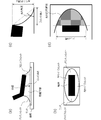
図3(a)~図3(d)に、はんだの各部の名称とはんだ形状を表す製品状態値の一例を示す。図3(a)は基板に平行な方向からはんだを見た側面図であり、図3(b)は基板の上方からはんだを見た平面図である。また、図3(c)、図3(d)はそれぞれ図3(a)、図3(b)の一部を拡大して示した図である。説明の便宜のため、部品本体等は図示を省略している。
本実施形態では、はんだ全体を「フロントフィレット」「バックフィレット」「右サイドフィレット」「左サイドフィレット」「電極下部」の5つの部分に分けて認識する。フロントフィレットは、部品電極の先端側に形成されたはんだフィレット部分であり、バックフィレットは、部品電極の後端側に形成されたはんだフィレット部分である。右サイドフィレットは部品電極の後端側から先端側を見たときに部品電極の右側にあるはんだフィレット部分である。また、左サイドフィレットは部品電極の後端側から先端側を見たときに部品電極の左側にあるはんだフィレット部分である。電極下部は、電極の真下にあるはんだ部分をさす。
図3(c)、図3(d)に示すように、各はんだフィレットの形状について、「ぬれ角度」「ぬれ広がり面積」「ぬれ上がり高さ」「フィレット長さ」「フィレット幅」の5項目の製品状態値を定義する。ぬれ角度は、フィレットの傾斜角であり、本実施形態では、フィレットの頂点と端点を結ぶ直線とランドとのなす角をフィレットの傾斜角と定義する。ぬれ広がり面積は、はんだとランドの接触部分(図の斜線部)の面積である。ぬれ上がり高さは、ランドに対するフィレットの頂点の高さである。フィレット長さとフィレット幅は、はんだとランドの接触部分における最大長さと最大幅である。なお、長さ方向はフレットの頂点と端点を結ぶ直線に平行な方向であり、幅方向は長さ方向に直交する方向と定義する。また、電極下部に関しては、図3(a)に示すように、「はんだ高さ」の1項目の製品状態値を定義する。はんだ高さは、電極下部の中央部におけるはんだの厚みである。
これらの製品状態値は、外観検査装置Y3での形状計測結果や、X線検査装置Y4での形状計測結果を基に求めることができる。各々の状態値の具体的な計算手法はどのようなアルゴリズムを用いてもよい。例えば、カラーハイライト方式で得られた外観画像からRGBの色相が現れている部分を抽出することで、はんだフィレットを切り出し、ぬれ広がり面積、フィレット長さ、フィレット幅を計算できる。そして、レーザ変位計や位相シフト法によりぬれ上がり高さを計測できれば、計算によりぬれ角度を求めることができる。
図4は、検査管理装置Y5に記録される製品状態値データの例を示す。製品状態値データには、基板ID、回路番号、ランドID、グループIDとともに、一つ以上の製品状態値が対応づけて記録されている。この製品状態値データの各行が、一つのはんだ(つまり、一つのランド)から計測された情報を示している。なお、ランドIDとは、回路内のランドの場所を特定する情報であり、例えば、8本の電極をもつ部品の場合は、ランドIDは1~8の値をとる。また、グループIDとは、ランドと電極の形状が同じであり、形成されるはんだが同じ形状であるべきもの(つまり、製品状態値を同一の基準で管理・評価できるもの)を示す情報である。例えば、グループIDは部品品番に対して割り当てられ、基板上に同じ品番の部品が複数配置される場合は、同一のグループIDを割り当てられたランドは全て、共通のグループIDとなる。また、一つの部品内に電極またはランドの形状が異なり、異なる形状のはんだが形成され得るランドがある場合には(例えば、QFP(Quad Flat Package)の端ピンとそれ以外のピンなど)、同一形状のはんだが形成されるランドに対し、それぞれ同じグループIDを割り当てることもできる。
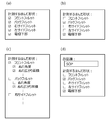
ところで、部品種やランド設計によって、形成されるはんだの形状は相違する。例えば、電極のピッチが狭く、ランド幅も狭い場合には、サイドフィレットはほとんど形成されないし、ランド長さが短い場合には、フロントフィレットがかなり小さくなることもある。そこで、検査管理装置Y5や分析装置Y6や作業端末Y7において、ユーザが部品種ごと又はランドごとに、計測の対象とするはんだ形状(製品状態値)を選択できるようにするとよい。図5(a)~図5(d)は計測の対象を選択するユーザインタフェースの一例である。図5(a)は、ランドサイズが標準の場合に、フロントフィレット、バックフィレット、右サイドフィレット、左サイドフィレット、電極下部の5つの部位の製品状態値をすべて計測するように設定した例である。図5(b)は、ランドの長さが短めの場合に、バックフィレットと電極下部の2つの部位の製品状態値のみを計測するように限定した例である。また、図5(c)は、計測する製品状態値を個別に選択できるようにしたユーザインターフェイスの例であり、図5(d)は、プルダウンメニューから部品種を選ぶと、自動的に適切な計測対象が設定される例である。このように部品種やランド設計に応じて計測対象とする製品状態値を限定できるようにすることで、製品状態値の計測や計算に要する時間を短縮できる。なお、これらの製品状態値は、後述する異常検知処理において異常の有無の評価に用いられるが、部品種やランド設計に応じて評価の対象とする項目を適宜設定しておけば、過剰な品質管理や異常検知を回避できるという効果もある(異常検知の詳細は後述する)。
<はんだ接合状態の判定>
外観検査装置Y3では、フロントフィレットが十分形成されていることを良品の条件とすることが一般的である。電極下面やバックフィレットの形状は外観検査装置Y3では直接観測できないからである。しかし、はんだと部品電極のあいだの接合強度は、フロントフィレットの部分だけでなく、電極下面とはんだの接合部や、バックフィレットの部分の寄与も大きい。それゆえ、外観検査の結果だけに頼ると、いわゆる見過ぎの発生を避けられない。
外観検査装置Y3では、フロントフィレットが十分形成されていることを良品の条件とすることが一般的である。電極下面やバックフィレットの形状は外観検査装置Y3では直接観測できないからである。しかし、はんだと部品電極のあいだの接合強度は、フロントフィレットの部分だけでなく、電極下面とはんだの接合部や、バックフィレットの部分の寄与も大きい。それゆえ、外観検査の結果だけに頼ると、いわゆる見過ぎの発生を避けられない。
図6(a)、図6(b)にその一例を示す。図6(a)は部品のマウント位置が正しい場合のはんだ形状を示しており、図6(b)は部品のマウント位置が電極の先端方向にずれた場合のはんだ形状の変化を示している。図6(a)では、フロントフィレットが十分に形成されているため、外観検査でOK判定となり、正しい検査結果が得られる。一方、部品が電極の先端方向にずれると、図6(b)に示すように、フロントフィレットが縮小してしまう。この場合、バックフィレットが十分に形成されているため接合強度が確保されているにもかかわらず(つまりはんだの接合状態は良好であるにもかかわらず)、外観検査ではNG判定されてしまい、不良基板として破棄されたり、生産設備の異常と誤検知し無駄にラインを止めることになる。これが見過ぎによる効率低下を生むのである。
本実施形態では、図6(b)のようなケースの良否を正しく判定するために、X線検査装置Y4の検査結果を基にはんだの最終的な良否判定を行う。電極とはんだではX線吸収率が異なるため、X線像(X線透過像又は断層像)において電極部分とはんだ部分のあいだに輝度差が生じる。よって、X線像を解析することで、電極下面における電極とはんだの接合の有無を調べたり、電極とはんだの接合面積(接合強度に相当)を計測したりすることができる。
<異常検知処理>
次に、分析装置Y6による異常検知処理について説明する。異常検知処理とは、ラインの稼働中、はんだの接合品質を常に監視することで、各生産設備X1~X3の異常を検知し、必要に応じて設備の動作条件にフィードバックする処理である。
次に、分析装置Y6による異常検知処理について説明する。異常検知処理とは、ラインの稼働中、はんだの接合品質を常に監視することで、各生産設備X1~X3の異常を検知し、必要に応じて設備の動作条件にフィードバックする処理である。
図7は、分析装置Y6の異常検知処理にかかわる機能ブロックを示している。分析装置Y6は、検査結果取得部60、設備情報取得部61、製品情報取得部62、良品分布作成用データベース63、データ更新部64、判定部65、異常検知部66などの機能を有している。これらの機能は、分析装置Y6(のCPU)がコンピュータプログラムを実行することにより実現されるものである。なお、図7では、分析装置Y6が有する機能のうち、異常検知処理に関する機能だけを示しており、他の機能については省略している。
図8のフローチャートに沿って、異常検知処理の流れと各機能ブロックの具体的な処理内容について説明する。図8の処理は、X線検査装置Y4から一つの基板の検査結果が得られたことをトリガとして実行される。
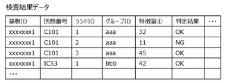
まず、検査結果取得部60が、X線検査装置Y4から(又は検査管理装置Y5を介して)検査結果のデータを取得する(ステップS80)。検査結果のデータには、図9に示すように、基板ID、回路番号、ランドID、グループID、はんだの接合状態を表す特徴量の値、その特徴量の値に対する判定結果などが含まれる。接合状態を表す特徴量としては、例えば、電極とはんだの接合面積、X線像における電極部分と周囲の輝度差、バックフィレットの長さ・幅・面積などを用いることができる。なお、接合状態を表す特徴量と判定結果の組は、一つの項目だけでもよいし、複数項目でもよい。以下、検査結果が得られた基板(基板IDで特定される基板)を「対象基板」と呼ぶ。
次に、設備情報取得部61が、基板IDに基づいて、対象基板の設備状態値データを生産設備管理装置X4から取得する(ステップS81)。設備状態値データの内容は、図2(a)~図2(c)に示したとおりである。また、製品情報取得部62が、基板IDに基づいて、対象基板の製品状態値データを検査管理装置Y5から取得する(ステップS82)。製品状態値データの内容は、図4に示したとおりである。
ステップS80~S82により、対象基板に関する、はんだ接合状態の最終的な検査結果データ、当該基板を処理したときの各生産設備の設備状態値データ、及び、各ランドに形成されたはんだの製品状態値データがそろう。続いて、対象基板上の個々のランド(はんだ)に対して、ステップS83以降の処理が実行される。以下、処理対象のランドを「対象ランド」と呼ぶ。
ステップS83では、判定部65が、対象ランドの検査結果を参照し、接合状態を表す特徴量がすべてOK判定か否かを確認する。すべての項目でOK判定が得られている場合には(ステップS83;YES)、対象ランドを良品と判定し、データ更新部64が、対象ランドのはんだの製品状態値データ(図4参照)及び設備状態値データ(図2(a)~図2(c)参照)を、良品分布作成用データベース63に追加する(ステップS84)。
良品分布作成用データベース63は、過去に生産された複数の良品に関する製品状態値及び設備状態値のデータ群を蓄積する記憶部である。ここに蓄積されたデータ群は、製品状態値や設備状態値の良品分布を評価するために利用される。初期状態(例えば、量産試作の開始時)では、良品分布作成用データベース63は空であるが、ラインの稼働に伴いデータの蓄積が進んでいき、良品分布の信頼性が高まっていく。なお、非常に古いデータや生産ロットが変わる前のデータなどは、良品分布を評価する際に妥当でない場合があるため、データ更新部64は、定期的に又は生産ロットが変わったタイミングで、過去のデータを削除する処理を行ってもよい。
ところで、ステップS83において、対象ランドの接合状態を表す特徴量のなかにNG判定のものが一つでも存在した場合には、判定部65は、対象ランドを不良品と判定し、ステップS85に処理を進める。なお、ステップS85以降の処理では製品状態値と設備状態値の良品分布を参照するため、もし、良品分布作成用データベース63が空であったり、十分なデータ蓄積がない場合には、ステップS85以降をスキップし、異常検知処理を中断するとよい。以下、良品分布作成用データベース63内に十分なデータが蓄積されているという前提で説明を進める。
ステップS85では、判定部65が、対象ランドのはんだ(不良品)の製品状態値データを取得する。そして、判定部65は、対象ランドとグループIDが同じ良品の製品状態値データを良品分布作成用データベース63から読み込み、製品状態値の良品分布を作成する(ステップS86)。製品状態値データの中に複数項目の製品状態値が含まれている場合には、製品状態値ごとに良品分布を作成する。図10(a)に製品状態値の良品分布の例を示す。本実施形態では、良品の製品状態値の平均μと標準偏差σを計算し、良品の製品状態値のばらつきを正規分布で近似する。ただし、良品分布の作成方法はこれに限らず、ヒストグラム(度数分布)を用いてもよい。
続いて、判定部65は、各々の製品状態値について、良品分布と対象ランド(不良品)の値を比較し、対象ランド(不良品)の値が通常範囲(良品範囲)に収まっているか異常値であるのかを判定する(ステップS87)。通常範囲は、例えば、良品分布のμ±nσに設定することができる。nの値は、要求品質に応じてユーザが設定可能であり、好ましくは2~5(典型的には3~4)に設定される。
ステップS87において、対象ランド(不良品)の製品状態値がすべて通常範囲(良品範囲)に収まっていると判定された場合、データ更新部64によって、良品分布の更新(学習)を行う(ステップS89)。ここでの更新は、対象ランド(不良品)の製品状態値が異常値と判定されやすくなるよう、良品分布を修正する操作である。具体的な操作としては、良品分布作成用データベース63に蓄積された良品のデータ群の中から、対象ランドの製品状態値と同じ値をもつ良品のデータ(同じ値のデータが無い場合は、最も近い値のデータ)を1サンプル分削除する。これにより、対象ランドの製品状態値が通常範囲と判定される確率を低下させることができる。良品分布の更新操作は、他のやり方でもよい。例えば、対象ランドの製品状態値に最も近い値をもつnサンプル分(n>1)の良品データを削除してもよい。また、例外処理として、対象ランドの製品状態値が良品分布の平均μに近い場合には(例えば、μ±2σ以内など)、良品分布の更新を行わないことも好ましい。
ステップS89で良品分布の更新を行った場合には、ステップS87の処理を再実行し、対象ランド(不良品)の製品状態値と更新後の良品分布の比較を行う。更新後の良品分布との比較においても、対象ランドの製品状態値がすべて通常範囲に収まっていると判定された場合には、生産設備には異常がない(つまり、対象ランドの不良は特異な又は原因不明の事象)とみなし、異常検知処理を終了する。なお、2回目の評価の場合には(ステップS88)、良品分布の更新は行われない。
ステップS87の処理において、対象ランド(不良品)の製品状態値のなかに一つでも異常値を示すものが存在した場合、判定部65は、生産設備に異常が生じている可能性ありと判断し、ステップS90へと処理を進める。ステップS90では、判定部65が、対象ランドのはんだ(不良品)に関する設備状態値データを取得する。そして、判定部65は、製品状態値の良品分布の作成に用いた複数の良品それぞれに対応する設備状態値データを良品分布作成用データベース63から読み込み、設備状態値の良品分布を作成する(ステップS91)。設備状態値データの中に複数項目の設備状態値が含まれている場合には、設備状態値ごとに良品分布を作成する。図10(b)に設備状態値の良品分布の例を示す。本実施形態では、製品状態値の良品分布と同じく、設備状態値の平均μと標準偏差σを計算し、良品の設備状態値のばらつきを正規分布で近似する。ただし、良品分布の作成方法はこれに限らず、ヒストグラム(度数分布)を用いてもよい。
続いて、判定部65は、各々の設備状態値について、良品分布と対象ランド(不良品)の値を比較し、対象ランド(不良品)の値が通常範囲(良品範囲)に収まっているか異常値であるのかを判定する(ステップS92)。通常範囲は、例えば、良品分布のμ±nσに設定することができる。nの値は、要求品質や設備性能に応じてユーザが設定可能であり、好ましくは2~5(典型的には3~4)に設定される。製品状態値と設備状態値とで通常範囲の設定(nの値)を異ならせても構わない。
ステップS92において、対象ランド(不良品)を処理したときの設備状態値がすべて通常範囲(良品範囲)に収まっていると判定された場合、判定部65は、生産設備には異常がないと判定し、異常検知処理を終了する(ステップS92;YES)。
一方、ステップS92において、対象ランド(不良品)を処理したときの設備状態値のなかに一つでも異常値を示すものが存在した場合、異常検知部66は、生産設備に異常が生じていると判断し、必要な対処を実行する(ステップS93)。例えば、ユーザに異常の発生を通知するために、異常の疑いのある生産設備を特定する情報(例えば設備名称)、異常を示した設備状態値、とり得る対策(例えば、動作条件の変更、修理やリセット方法など)などの情報を、分析装置や作業端末や該当する生産設備に出力することができる。このとき、不良品に関する情報(対象基板と対象ランドを特定する情報、NG判定された接合状態を表す特徴量とその値など)、異常を示した製品状態値、設備状態値と製品状態値の良品分布などの情報を出力することも好ましい。情報の出力方法は、モニタへの表示、プリンタへの印刷、スピーカでの音声出力、メール送信などどのような方法でもよい。あるいは、異常検知部66は、異常を是正するために生産設備の動作条件をどのように変更すればよいか判断し、該当する生産設備の動作条件(実装プログラムなど)を変更してもよい。この場合、異常検知部66は、生産設備の動作条件を自動で変更してもよいし、分析装置や作業端末や生産設備のモニタに「動作条件を変更しますか?」と表示するなどして、変更の可否をユーザに問い合わせ、ユーザから変更許可を受け付けた上で動作条件の変更処理を実行してもよい。
以上の処理をすべてのランドに対して実行すると、図8の異常検知処理が完了する。図11は、具体的なケースを用いて、図8の異常検知処理の挙動を説明する図である。この例では、接合状態を表す特徴量、設備状態値、製品状態値をそれぞれ2項目ずつ用いている。
(1)ケース1は、接合状態を表す特徴量がいずれもOK判定の場合である。この場合は、対象ランドは良品と判断され、対象ランドに関する設備状態値データ及び製品状態値データが良品分布のデータ群に追加される(ステップS83;YES→S84)。ケース1では、対象ランドの設備状態値や製品状態値については一切評価しないため、図10のようにたとえ設備状態値や製品状態値のなかに異常値(良品範囲外)のものが含まれていたとしても、接合状態を表す特徴量(はんだ形状の最終的な良否判断)が優先される。
(2)ケース2は、接合状態を表す特徴量のなかにNG判定のものが含まれているが、対象ランドの製品状態値がすべて良品範囲内にあるというケースである。この場合、(対象ランドは不良品であるものの)生産設備には異常なしと判断し、生産設備へのフィードバックは行わない(ステップS87;YES)。
(3)ケース3は、接合状態を表す特徴量のなかにNG判定のものが含まれており、対象ランドの製品状態値のなかに異常値(良品範囲外)のものが含まれているというケースである。この場合に初めて生産設備の設備状態値の評価が行われ、異常値(良品範囲外)を示すものがあれば、生産設備に異常ありと判断する。
<本実施形態の利点>
上述した本実施形態の構成によれば、はんだの接合状態が不良と判定され、当該不良品のはんだ形状の状態(製品状態値)が良品分布との比較において異常値であり、且つ、当該不良品を処理したときの生産設備の状態(設備状態値)が良品分布との比較において異常値である、という条件を満足した場合に、生産設備に異常があると判断し、ユーザ又は生産設備へのフィードバックを行う。したがって、製品の最終品質に影響を及ぼし、且つ、製品の状態と生産設備の状態のいずれもが通常状態から乖離している状態だけを検出できるため、生産設備の異常の誤報(過剰な品質管理)を抑制することができる。また、本実施形態では、X線検査の検査結果を用いるので、外観からはわからないはんだと電極との接合状態を精度よく捉えることができ、良品か不良品かの誤判定を可及的に無くすことができ、過剰な品質管理を抑制することができる。しかも、部品種やランド仕様に応じて、判定の対象とする製品状態値を選択(限定)できるようにしたので、処理の高速化と過剰な品質管理の抑制を図ることができる。また、生産ラインを実稼働するなかで得られた良品や不良品の情報を用いて良品分布を自動的に更新(学習)していくことにより、良品分布の信頼性、ひいては異常判断の妥当性や確度を高めることができる。
上述した本実施形態の構成によれば、はんだの接合状態が不良と判定され、当該不良品のはんだ形状の状態(製品状態値)が良品分布との比較において異常値であり、且つ、当該不良品を処理したときの生産設備の状態(設備状態値)が良品分布との比較において異常値である、という条件を満足した場合に、生産設備に異常があると判断し、ユーザ又は生産設備へのフィードバックを行う。したがって、製品の最終品質に影響を及ぼし、且つ、製品の状態と生産設備の状態のいずれもが通常状態から乖離している状態だけを検出できるため、生産設備の異常の誤報(過剰な品質管理)を抑制することができる。また、本実施形態では、X線検査の検査結果を用いるので、外観からはわからないはんだと電極との接合状態を精度よく捉えることができ、良品か不良品かの誤判定を可及的に無くすことができ、過剰な品質管理を抑制することができる。しかも、部品種やランド仕様に応じて、判定の対象とする製品状態値を選択(限定)できるようにしたので、処理の高速化と過剰な品質管理の抑制を図ることができる。また、生産ラインを実稼働するなかで得られた良品や不良品の情報を用いて良品分布を自動的に更新(学習)していくことにより、良品分布の信頼性、ひいては異常判断の妥当性や確度を高めることができる。
<その他>
上記の実施形態の説明は、本発明を例示的に説明するものに過ぎず、本発明は上記の具体的な形態には限定されない。本発明は、その技術的思想の範囲内で種々の変形が可能である。
例えば上記実施形態では、X線検査によりはんだの接合状態の良否を判定したが、他の検査手段を用いてもよい。例えば、外観検査装置、超音波による非破壊検査装置、導通テストにより接合状態を検査する装置などを用いてもよいし、あるいは、オペレータが目視検査を行い、その結果を検査管理装置に入力するようにしてもよい。
また、上記実施形態では表面実装ラインを例示したが、本発明は、表面実装ラインに限らず、一つ以上の生産設備を含む生産ラインであればどのような種類の生産ラインの品質管理にも好ましく適用することができる。
また、上記実施形態では、図3(a)~図3(d)のように、はんだ全体を5つの部分に分けて認識したが、これはあくまで一例であり、フロントフィレット・バックフィレット・電極下部の3つの部分に分ける方法など、他の分け方を採用してもよい。また、はんだフィレットについて「ぬれ角度」「ぬれ広がり面積」「ぬれ上がり高さ」「フィレット長さ」「フィレット幅」の5項目の製品状態値、電極下部について「はんだ高さ」の1項目の製品状態値を計測したが、これも一例にすぎず、他の製品状態値を用いてもよい。たとえば、ランド側のぬれ角度と電極側のぬれ角度をそれぞれ計測してもよいし、フィレット幅についても電極先端部分の幅とランド先端部分の幅をそれぞれ計測してもよい。
上記の実施形態の説明は、本発明を例示的に説明するものに過ぎず、本発明は上記の具体的な形態には限定されない。本発明は、その技術的思想の範囲内で種々の変形が可能である。
例えば上記実施形態では、X線検査によりはんだの接合状態の良否を判定したが、他の検査手段を用いてもよい。例えば、外観検査装置、超音波による非破壊検査装置、導通テストにより接合状態を検査する装置などを用いてもよいし、あるいは、オペレータが目視検査を行い、その結果を検査管理装置に入力するようにしてもよい。
また、上記実施形態では表面実装ラインを例示したが、本発明は、表面実装ラインに限らず、一つ以上の生産設備を含む生産ラインであればどのような種類の生産ラインの品質管理にも好ましく適用することができる。
また、上記実施形態では、図3(a)~図3(d)のように、はんだ全体を5つの部分に分けて認識したが、これはあくまで一例であり、フロントフィレット・バックフィレット・電極下部の3つの部分に分ける方法など、他の分け方を採用してもよい。また、はんだフィレットについて「ぬれ角度」「ぬれ広がり面積」「ぬれ上がり高さ」「フィレット長さ」「フィレット幅」の5項目の製品状態値、電極下部について「はんだ高さ」の1項目の製品状態値を計測したが、これも一例にすぎず、他の製品状態値を用いてもよい。たとえば、ランド側のぬれ角度と電極側のぬれ角度をそれぞれ計測してもよいし、フィレット幅についても電極先端部分の幅とランド先端部分の幅をそれぞれ計測してもよい。
60:検査結果取得部、61:設備情報取得部、62:製品情報取得部、63:良品分布作成用データベース、64:データ更新部、65:判定部、66:異常検知部
X1:はんだ印刷装置、X2:マウンタ、X3:リフロー炉、X4:生産設備管理装置
Y1:印刷検査装置、Y2:部品検査装置、Y3:外観検査装置、Y4:X線検査装置、Y5:検査管理装置、Y6:分析装置、Y7:作業端末
X1:はんだ印刷装置、X2:マウンタ、X3:リフロー炉、X4:生産設備管理装置
Y1:印刷検査装置、Y2:部品検査装置、Y3:外観検査装置、Y4:X線検査装置、Y5:検査管理装置、Y6:分析装置、Y7:作業端末
Claims (10)
- 一つ以上の生産設備を含む生産ラインの品質管理を行う品質管理装置であって、
生産設備で製品を処理するときに観測された、前記生産設備の状態を表す設備状態値のデータを取得する設備情報取得部と、
前記生産設備で処理された製品から計測された、前記製品の状態を表す製品状態値のデータを取得する製品情報取得部と、
過去に生産された複数の良品に関する設備状態値のデータ群と、前記複数の良品に関する製品状態値のデータ群とを記憶する記憶部と、
ある製品が不良品と判定された場合に、前記記憶部に蓄積された複数の良品の製品状態値のデータ群からなる製品状態値の良品分布との比較により、当該不良品の製品状態値が異常値であるか否かを判定すると共に、前記記憶部に蓄積された複数の良品の設備状態値のデータ群からなる設備状態値の良品分布との比較により、当該不良品を処理したときの設備状態値が異常値であるか否かを判定する判定部と、
前記不良品に関する製品状態値と設備状態値のいずれもが異常値と判定された場合に、前記生産設備に異常があると判断する異常検知部と、
を有することを特徴とする品質管理装置。 - ある製品が良品と判定された場合に、当該製品の製品状態値を、前記記憶部に蓄積されている製品状態値のデータ群に追加する更新部をさらに有する
ことを特徴とする請求項1に記載の品質管理装置。 - ある製品が不良品と判定された場合であって、且つ、前記判定部により当該不良品の製品状態値が異常値でないと判定された場合に、
前記更新部は、当該不良品の製品状態値が異常値と判定されやすくなるように、前記記憶部に記憶された製品状態値のデータ群の一部のデータを削除する
ことを特徴とする請求項2に記載の品質管理装置。 - 前記異常検知部は、前記生産設備に異常があると判断した場合に、異常の情報を出力するか、又は、前記生産設備の動作条件を自動で変更するか、又は、前記生産設備の動作条件の変更許可をユーザから受け付けた後に前記生産設備の動作条件を変更する
ことを特徴とする請求項1~3のうちいずれか1項に記載の品質管理装置。 - 前記異常の情報は、異常があると判断された生産設備を特定する情報、異常値と判定された設備状態値、不良品と判定された製品を特定する情報、及び、異常値と判定された製品状態値のうち少なくともいずれかを含む
ことを特徴とする請求項4に記載の品質管理装置。 - 前記判定部は、同じ製品から計測された複数の項目の製品状態値のそれぞれについて異常値であるか否かを判定可能であり、
前記複数の項目のうち判定の対象とする項目を選択可能である
ことを特徴とする請求項1~5のうちいずれか1項に記載の品質管理装置。 - 前記生産ラインは、プリント基板の表面実装ラインであり、
前記生産設備は、プリント基板の上にはんだペーストを印刷するはんだ印刷装置、プリント基板の上に電子部品を実装するマウンタ、はんだペーストを加熱するリフロー炉のうちの少なくとも一つであり、
前記製品の状態は、リフロー後のはんだの形状である
ことを特徴とする請求項1~6のうちいずれか1項に記載の品質管理装置。 - はんだが良品であるか不良品であるかの判定結果は、X線像によりはんだと電子部品の電極との接合状態を検査するX線検査装置から取得される
ことを特徴とする請求項7に記載の品質管理装置。 - 一つ以上の生産設備を含む生産ラインの品質管理を行う品質管理装置の制御方法であって、
生産設備で製品を処理するときに観測された、前記生産設備の状態を表す設備状態値のデータを取得する設備情報取得ステップと、
前記生産設備で処理された製品から計測された、前記製品の状態を表す製品状態値のデータを取得する製品情報取得ステップと、
ある製品が不良品と判定された場合に、過去に生産された複数の良品に関する製品状態値のデータ群からなる製品状態値の良品分布との比較により当該不良品の製品状態値が異常値であるか否かを判定する製品状態判定ステップと、
前記複数の良品に関する設備状態値のデータ群からなる設備状態値の良品分布との比較により前記不良品を処理したときの設備状態値が異常値であるか否かを判定する設備状態判定ステップと、
前記不良品に関する製品状態値と設備状態値のいずれもが異常値と判定された場合に、前記生産設備に異常があると判断する異常検知ステップと、
を有することを特徴とする品質管理装置の制御方法。 - 請求項9に記載の品質管理装置の制御方法の各ステップをコンピュータに実行させるためのプログラム。
Priority Applications (2)
| Application Number | Priority Date | Filing Date | Title |
|---|---|---|---|
| EP15746444.7A EP3106948B1 (en) | 2014-02-10 | 2015-02-06 | Quality control apparatus and control method |
| CN201580005005.6A CN105940354B (zh) | 2014-02-10 | 2015-02-06 | 品质管理装置及其控制方法、存储装置 |
Applications Claiming Priority (2)
| Application Number | Priority Date | Filing Date | Title |
|---|---|---|---|
| JP2014023318A JP6264072B2 (ja) | 2014-02-10 | 2014-02-10 | 品質管理装置及びその制御方法 |
| JP2014-023318 | 2014-02-10 |
Publications (1)
| Publication Number | Publication Date |
|---|---|
| WO2015119232A1 true WO2015119232A1 (ja) | 2015-08-13 |
Family
ID=53778032
Family Applications (1)
| Application Number | Title | Priority Date | Filing Date |
|---|---|---|---|
| PCT/JP2015/053339 Ceased WO2015119232A1 (ja) | 2014-02-10 | 2015-02-06 | 品質管理装置及びその制御方法 |
Country Status (4)
| Country | Link |
|---|---|
| EP (1) | EP3106948B1 (ja) |
| JP (1) | JP6264072B2 (ja) |
| CN (1) | CN105940354B (ja) |
| WO (1) | WO2015119232A1 (ja) |
Cited By (1)
| Publication number | Priority date | Publication date | Assignee | Title |
|---|---|---|---|---|
| JP2022055231A (ja) * | 2020-09-28 | 2022-04-07 | 横河電機株式会社 | データ処理システム、データ処理方法、および、データ処理プログラム |
Families Citing this family (34)
| Publication number | Priority date | Publication date | Assignee | Title |
|---|---|---|---|---|
| JP6915981B2 (ja) * | 2016-11-17 | 2021-08-11 | ハンファ精密機械株式会社 | 電子部品実装システム及び電子部品実装方法 |
| JP6653307B2 (ja) * | 2016-11-25 | 2020-02-26 | 花王株式会社 | 製品の製造方法及び製品の製造装置 |
| TWI741074B (zh) * | 2016-11-25 | 2021-10-01 | 日商花王股份有限公司 | 製品之製造方法及製品之製造裝置 |
| JP6880843B2 (ja) * | 2017-03-09 | 2021-06-02 | オムロン株式会社 | 管理装置および管理プログラム |
| CN106932537A (zh) * | 2017-03-20 | 2017-07-07 | 成都乾威科技有限公司 | 一种车用尿素的生产数据处理方法及装置 |
| JP6514260B2 (ja) * | 2017-04-13 | 2019-05-15 | ファナック株式会社 | 制御装置及び機械学習装置 |
| US10482382B2 (en) * | 2017-05-09 | 2019-11-19 | Palantir Technologies Inc. | Systems and methods for reducing manufacturing failure rates |
| KR102168737B1 (ko) * | 2017-07-19 | 2020-10-22 | 미쓰비시덴키 가부시키가이샤 | 품질 분석 장치 및 품질 분석 방법 |
| JP7134453B2 (ja) * | 2017-09-05 | 2022-09-12 | 株式会社Kmc | 生産監視システム及び生産監視方法 |
| CN111512252A (zh) * | 2017-12-28 | 2020-08-07 | 豪迈面板分割科技有限公司 | 用于加工工件的方法以及加工系统 |
| JP7190624B2 (ja) * | 2018-01-31 | 2022-12-16 | パナソニックIpマネジメント株式会社 | 実装ライン管理システム及び実装ラインの管理方法 |
| JP6959879B2 (ja) * | 2018-02-08 | 2021-11-05 | 株式会社Screenホールディングス | データ処理方法、データ処理装置、および、データ処理プログラム |
| CN109062183B (zh) * | 2018-07-31 | 2021-05-11 | 杭州休伦科技有限公司 | 新能源汽车远程监控分析方法和系统 |
| JP6977686B2 (ja) | 2018-08-06 | 2021-12-08 | オムロン株式会社 | 制御システムおよび制御装置 |
| JP7349596B2 (ja) * | 2018-12-27 | 2023-09-25 | パナソニックIpマネジメント株式会社 | 基板処理システム |
| CN111421954B (zh) * | 2019-01-10 | 2022-02-18 | 鸿富锦精密电子(天津)有限公司 | 智能判定回馈方法及装置 |
| CN109741927B (zh) * | 2019-03-14 | 2020-08-07 | 贵港市嘉龙海杰电子科技有限公司 | 微型变压器生产线的设备故障和潜在不良品智能预测系统 |
| HUE067302T2 (hu) * | 2019-04-02 | 2024-10-28 | Cybord Ltd | Rendszer és módszer a hamisított és kiberelektronikai alkatrészek felismerésére |
| JP7437784B2 (ja) * | 2019-04-22 | 2024-02-26 | パナソニックIpマネジメント株式会社 | 学習済みモデルの生成方法、保全表示装置、及びプログラム |
| CN110031042A (zh) * | 2019-04-25 | 2019-07-19 | 伟创力电子设备(深圳)有限公司 | Pcba制造的三段式检测方法及装置 |
| CN113710487B (zh) * | 2019-04-26 | 2022-10-21 | 株式会社富士 | 印刷参数取得装置以及印刷参数取得方法 |
| CN110108717A (zh) * | 2019-05-15 | 2019-08-09 | 广东工业大学 | 一种显示模组生产设备状态评估方法,装置及系统 |
| JP7151636B2 (ja) * | 2019-06-14 | 2022-10-12 | 東芝三菱電機産業システム株式会社 | データ収集装置 |
| JP7369905B2 (ja) * | 2019-07-09 | 2023-10-27 | パナソニックIpマネジメント株式会社 | 実装基板製造システムおよび実装基板製造方法 |
| EP3787014A1 (de) * | 2019-08-29 | 2021-03-03 | Siemens Aktiengesellschaft | Erfassung von prozessparametern einer montagelinie |
| CN112579640B (zh) | 2019-09-29 | 2024-09-20 | 京东方科技集团股份有限公司 | 用于生产异常检测的方法和设备 |
| JP7511140B2 (ja) * | 2019-11-14 | 2024-07-05 | パナソニックIpマネジメント株式会社 | 学習済みモデルの生成方法、装置、およびプログラム |
| DE102020207247A1 (de) | 2020-06-10 | 2021-12-16 | Sms Group Gmbh | System, Verfahren und Computerprogramm zur Steuerung einer aus mehreren Anlagenteilen bestehenden Produktionsanlage, insbesondere einer metallurgischen Produktionsanlage zur Erzeugung von Industriegütern wie metallischem Halbzeug und/oder metallischen Endprodukten |
| WO2022224657A1 (ja) * | 2021-04-19 | 2022-10-27 | 富士フイルム株式会社 | 製造ラインの異常予兆検知装置、方法及びプログラム並びに製造装置及び検品装置 |
| KR102474332B1 (ko) * | 2021-05-10 | 2022-12-05 | 충북대학교 산학협력단 | 스마트 공장 시스템에서 설비 건강 안정도 예측 방법 및 이를 기록한 기록매체 |
| JP7702637B2 (ja) * | 2021-07-16 | 2025-07-04 | パナソニックIpマネジメント株式会社 | 部品データ管理方法、部品データ管理装置、部品データ管理プログラムならびに部品データ管理システム |
| MX2024001470A (es) * | 2021-08-02 | 2024-02-27 | Arch Systems Inc | Metodo de analisis y/o mantenimiento de sistemas de fabricacion. |
| CN114265390B (zh) * | 2021-12-22 | 2024-02-20 | 苏州华星光电技术有限公司 | 设备数据采集诊断方法、装置、服务器及存储介质 |
| CN114633042B (zh) * | 2022-05-19 | 2022-08-30 | 深圳市大族封测科技股份有限公司 | 球焊质量监控方法、控制器及系统 |
Citations (4)
| Publication number | Priority date | Publication date | Assignee | Title |
|---|---|---|---|---|
| JP2007079933A (ja) * | 2005-09-14 | 2007-03-29 | Sharp Corp | 製造情報処理方法及びそれをコンピュータに実行させるためのプログラム並びに製造情報管理システム |
| JP2008108815A (ja) * | 2006-10-24 | 2008-05-08 | Sharp Corp | 不良原因設備特定システム |
| JP2009140044A (ja) * | 2007-12-04 | 2009-06-25 | Renesas Technology Corp | 製造装置異常検査システム |
| JP2010191744A (ja) * | 2009-02-19 | 2010-09-02 | Seiko Epson Corp | 処理装置の管理方法及びその管理システム |
Family Cites Families (10)
| Publication number | Priority date | Publication date | Assignee | Title |
|---|---|---|---|---|
| JP3344739B2 (ja) * | 1992-09-30 | 2002-11-18 | 松下電器産業株式会社 | 実装基板生産システムおよび実装基板生産方法 |
| JPH10275842A (ja) * | 1997-03-31 | 1998-10-13 | Hitachi Ltd | 薄膜製品の製造方法および薄膜製品の製造ライン管理システム |
| JP3818308B2 (ja) * | 2005-02-01 | 2006-09-06 | オムロン株式会社 | プリント基板の品質管理システム |
| JP4552749B2 (ja) * | 2005-05-12 | 2010-09-29 | オムロン株式会社 | 検査基準設定装置及び方法、並びに、工程検査装置 |
| JP5198087B2 (ja) * | 2008-02-21 | 2013-05-15 | 富士フイルム株式会社 | 製造設備の診断装置及び方法 |
| JP5158018B2 (ja) * | 2009-05-26 | 2013-03-06 | 新日鐵住金株式会社 | 生産システムの設備診断装置および設備診断方法、並びに設備診断プログラムおよびこれを記録したコンピュータ読み取り可能な記録媒体 |
| WO2011155012A1 (ja) * | 2010-06-07 | 2011-12-15 | パイオニア株式会社 | 品質管理システム、端末装置、情報処理方法及びセンタ装置用プログラム |
| JP5594886B2 (ja) * | 2010-10-19 | 2014-09-24 | 富士機械製造株式会社 | 部品実装ラインの管理装置 |
| JP5365643B2 (ja) * | 2011-01-13 | 2013-12-11 | オムロン株式会社 | はんだ付け検査方法、および基板検査システムならびにはんだ付け検査機 |
| JP5779906B2 (ja) * | 2011-02-25 | 2015-09-16 | オムロン株式会社 | 検査システム、管理サーバ、検査装置および検査データ管理方法 |
-
2014
- 2014-02-10 JP JP2014023318A patent/JP6264072B2/ja active Active
-
2015
- 2015-02-06 EP EP15746444.7A patent/EP3106948B1/en active Active
- 2015-02-06 CN CN201580005005.6A patent/CN105940354B/zh active Active
- 2015-02-06 WO PCT/JP2015/053339 patent/WO2015119232A1/ja not_active Ceased
Patent Citations (4)
| Publication number | Priority date | Publication date | Assignee | Title |
|---|---|---|---|---|
| JP2007079933A (ja) * | 2005-09-14 | 2007-03-29 | Sharp Corp | 製造情報処理方法及びそれをコンピュータに実行させるためのプログラム並びに製造情報管理システム |
| JP2008108815A (ja) * | 2006-10-24 | 2008-05-08 | Sharp Corp | 不良原因設備特定システム |
| JP2009140044A (ja) * | 2007-12-04 | 2009-06-25 | Renesas Technology Corp | 製造装置異常検査システム |
| JP2010191744A (ja) * | 2009-02-19 | 2010-09-02 | Seiko Epson Corp | 処理装置の管理方法及びその管理システム |
Cited By (2)
| Publication number | Priority date | Publication date | Assignee | Title |
|---|---|---|---|---|
| JP2022055231A (ja) * | 2020-09-28 | 2022-04-07 | 横河電機株式会社 | データ処理システム、データ処理方法、および、データ処理プログラム |
| JP7218338B2 (ja) | 2020-09-28 | 2023-02-06 | 横河電機株式会社 | データ処理システム、データ処理方法、および、データ処理プログラム |
Also Published As
| Publication number | Publication date |
|---|---|
| EP3106948A1 (en) | 2016-12-21 |
| JP6264072B2 (ja) | 2018-01-24 |
| CN105940354A (zh) | 2016-09-14 |
| EP3106948B1 (en) | 2020-09-02 |
| JP2015152943A (ja) | 2015-08-24 |
| CN105940354B (zh) | 2019-02-12 |
| EP3106948A4 (en) | 2017-10-25 |
Similar Documents
| Publication | Publication Date | Title |
|---|---|---|
| JP6264072B2 (ja) | 品質管理装置及びその制御方法 | |
| JP6413246B2 (ja) | 品質管理装置および品質管理装置の制御方法 | |
| CN105917756B (zh) | 质量管理装置和质量管理方法 | |
| JP6812660B2 (ja) | 生産ラインの管理装置 | |
| CN100596267C (zh) | 基板检查用的基准值设定方法、利用该方法的装置及程序 | |
| JP6988499B2 (ja) | 検査管理システム、検査管理装置、検査管理方法 | |
| JP6922694B2 (ja) | 管理システム、管理装置、管理方法、及びプログラム | |
| JP2018025481A (ja) | 表面実装ラインの検査装置及び品質管理システム | |
| JP6451142B2 (ja) | 品質管理装置および品質管理装置の制御方法 | |
| JP6277754B2 (ja) | 品質管理システムおよび内部検査装置 | |
| JP7484733B2 (ja) | 管理システム、管理装置、管理方法、及びプログラム | |
| JP6988500B2 (ja) | 検査管理システム、検査管理装置、検査管理方法 | |
| JP6349734B2 (ja) | 品質管理装置、品質管理方法、およびプログラム | |
| CN104777166B (zh) | 内部检查装置的控制装置及其方法、程序及检查系统 | |
| JP7735660B2 (ja) | 検査管理システム、検査管理装置、検査管理方法、及びプログラム | |
| JP6387620B2 (ja) | 品質管理システム | |
| JP4661371B2 (ja) | 基板検査システム | |
| WO2022162961A1 (ja) | 管理装置及び管理システム | |
| JP2024102958A (ja) | 検査管理システム、検査管理装置、判定方法、及びプログラム | |
| JP2012124269A (ja) | プリント基板製造システム及び製造方法 |
Legal Events
| Date | Code | Title | Description |
|---|---|---|---|
| 121 | Ep: the epo has been informed by wipo that ep was designated in this application |
Ref document number: 15746444 Country of ref document: EP Kind code of ref document: A1 |
|
| REEP | Request for entry into the european phase |
Ref document number: 2015746444 Country of ref document: EP |
|
| WWE | Wipo information: entry into national phase |
Ref document number: 2015746444 Country of ref document: EP |
|
| NENP | Non-entry into the national phase |
Ref country code: DE |