WO2015133365A1 - Dispositif de conversion de puissance - Google Patents
Dispositif de conversion de puissance Download PDFInfo
- Publication number
- WO2015133365A1 WO2015133365A1 PCT/JP2015/055655 JP2015055655W WO2015133365A1 WO 2015133365 A1 WO2015133365 A1 WO 2015133365A1 JP 2015055655 W JP2015055655 W JP 2015055655W WO 2015133365 A1 WO2015133365 A1 WO 2015133365A1
- Authority
- WO
- WIPO (PCT)
- Prior art keywords
- bypass
- semiconductor
- short
- converter
- power conversion
- Prior art date
- Legal status (The legal status is an assumption and is not a legal conclusion. Google has not performed a legal analysis and makes no representation as to the accuracy of the status listed.)
- Ceased
Links
Images


Classifications
-
- H—ELECTRICITY
- H02—GENERATION; CONVERSION OR DISTRIBUTION OF ELECTRIC POWER
- H02M—APPARATUS FOR CONVERSION BETWEEN AC AND AC, BETWEEN AC AND DC, OR BETWEEN DC AND DC, AND FOR USE WITH MAINS OR SIMILAR POWER SUPPLY SYSTEMS; CONVERSION OF DC OR AC INPUT POWER INTO SURGE OUTPUT POWER; CONTROL OR REGULATION THEREOF
- H02M1/00—Details of apparatus for conversion
- H02M1/32—Means for protecting converters other than automatic disconnection
-
- H—ELECTRICITY
- H02—GENERATION; CONVERSION OR DISTRIBUTION OF ELECTRIC POWER
- H02M—APPARATUS FOR CONVERSION BETWEEN AC AND AC, BETWEEN AC AND DC, OR BETWEEN DC AND DC, AND FOR USE WITH MAINS OR SIMILAR POWER SUPPLY SYSTEMS; CONVERSION OF DC OR AC INPUT POWER INTO SURGE OUTPUT POWER; CONTROL OR REGULATION THEREOF
- H02M1/00—Details of apparatus for conversion
- H02M1/38—Means for preventing simultaneous conduction of switches
-
- H—ELECTRICITY
- H02—GENERATION; CONVERSION OR DISTRIBUTION OF ELECTRIC POWER
- H02M—APPARATUS FOR CONVERSION BETWEEN AC AND AC, BETWEEN AC AND DC, OR BETWEEN DC AND DC, AND FOR USE WITH MAINS OR SIMILAR POWER SUPPLY SYSTEMS; CONVERSION OF DC OR AC INPUT POWER INTO SURGE OUTPUT POWER; CONTROL OR REGULATION THEREOF
- H02M7/00—Conversion of AC power input into DC power output; Conversion of DC power input into AC power output
- H02M7/42—Conversion of DC power input into AC power output without possibility of reversal
- H02M7/44—Conversion of DC power input into AC power output without possibility of reversal by static converters
- H02M7/48—Conversion of DC power input into AC power output without possibility of reversal by static converters using discharge tubes with control electrode or semiconductor devices with control electrode
- H02M7/483—Converters with outputs that each can have more than two voltages levels
- H02M7/4835—Converters with outputs that each can have more than two voltages levels comprising two or more cells, each including a switchable capacitor, the capacitors having a nominal charge voltage which corresponds to a given fraction of the input voltage, and the capacitors being selectively connected in series to determine the instantaneous output voltage
-
- H—ELECTRICITY
- H02—GENERATION; CONVERSION OR DISTRIBUTION OF ELECTRIC POWER
- H02M—APPARATUS FOR CONVERSION BETWEEN AC AND AC, BETWEEN AC AND DC, OR BETWEEN DC AND DC, AND FOR USE WITH MAINS OR SIMILAR POWER SUPPLY SYSTEMS; CONVERSION OF DC OR AC INPUT POWER INTO SURGE OUTPUT POWER; CONTROL OR REGULATION THEREOF
- H02M1/00—Details of apparatus for conversion
- H02M1/32—Means for protecting converters other than automatic disconnection
- H02M1/322—Means for rapidly discharging a capacitor of the converter for protecting electrical components or for preventing electrical shock
-
- H—ELECTRICITY
- H02—GENERATION; CONVERSION OR DISTRIBUTION OF ELECTRIC POWER
- H02M—APPARATUS FOR CONVERSION BETWEEN AC AND AC, BETWEEN AC AND DC, OR BETWEEN DC AND DC, AND FOR USE WITH MAINS OR SIMILAR POWER SUPPLY SYSTEMS; CONVERSION OF DC OR AC INPUT POWER INTO SURGE OUTPUT POWER; CONTROL OR REGULATION THEREOF
- H02M1/00—Details of apparatus for conversion
- H02M1/32—Means for protecting converters other than automatic disconnection
- H02M1/325—Means for protecting converters other than automatic disconnection with means for allowing continuous operation despite a fault, i.e. fault tolerant converters
Definitions
- the present invention relates to a power conversion device in which a plurality of converter cells are connected in series.
- Non-Patent Documents 1 and 2 A multi-level converter having a circuit configuration that generates an AC voltage for V and W and a DC voltage for DC terminals P and N is disclosed (for example, see Non-Patent Documents 1 and 2).
- Non-Patent Document 1 uses a half-bridge converter cell called a chopper cell.
- Non-Patent Document 2 in addition to the half-bridge type, a converter cell constituted by a so-called full-bridge using two legs (legs) is also used.
- Makoto Sugawara, Yasufumi Akagi “PWM control method and operation verification of modular multi-level converter (MMC)”, IEEJ Transactions D, Vol. 128, No. 7, pp. 957-965, 2008 (p. 958, FIGS. 1 and 2) J. Dorn, etc. “Transformation of the Energy System in Germany-Enhancement of System Stability by Integration of innovative Multilevel HVDC in the AC Grid”, International ETG-Kongress 2013. Makoto Sugawara, Ryo Maeda, Yasufumi Akagi “Application of Modular Multilevel Cascade Converter (MMCC-SDBC) to STATCOM”, IEEJ Transactions D, Vol. 131, No. 12, pp.
- MMC modular multi-level converter
- this bypass element may be exposed to severe conditions such as overcurrent in connection with its closing operation, and if damaged by this severe use, it may not be possible to reliably bypass the converter cell in which an abnormality has occurred. . Thereby, the subsequent reliable opening / closing operation cannot be performed, and there is a problem that the continuation of the operation as the power conversion device cannot be compensated.
- the present invention has been made to solve the above-described problems.
- the bypass element that closes the output terminal is surely prevented from being damaged due to the closing operation.
- An object of the present invention is to obtain a power conversion device that can continue the process.
- the power converter according to the present invention is A plurality of converter cells for converting power are connected in series, and a power conversion device including a detection unit for detecting whether or not each of the converter cells is normal,
- the converter cell includes a plurality of semiconductor elements, an electrical energy storage element, an output terminal, and a bypass element having one end connected to the output terminal, When an abnormality of the converter cell is detected, the bypass element is closed, and at the same time or before the bypass element is closed, the bypass element is connected in parallel with the bypass element of the plurality of semiconductor elements.
- the semiconductor element selected so as to form a current path not including an element is turned on.
- the power converter according to the present invention is A plurality of converter cells for converting power are connected in series, and a power conversion device including a detection unit for detecting whether or not each of the converter cells is normal,
- the converter cell includes a plurality of semiconductor elements, an electrical energy storage element, an output terminal, and a bypass element having one end connected to the output terminal,
- a gate driving unit that drives gates of some of the semiconductor elements has an arm short-circuit protection unit that protects some of the semiconductor elements from damage due to a short-circuit current. It is.
- the overcurrent flowing through the bypass element can be suppressed, and a highly reliable power conversion device can be realized.
- FIG. 15 which makes the object of protection operation partially different. It is another figure which shows the flow explaining the protection operation of the same meaning as FIG. 15, which makes the object of protection operation partially different. It is a figure explaining the case where bypass element BP is closed by malfunctioning and an overcurrent flows. It is a figure explaining the case where bypass element BP is closed by malfunctioning and an overcurrent flows. It is a figure which shows the flow explaining the protection operation of the same meaning as FIG. 19 which makes the object of protection operation partially different. It is a figure which shows the flow explaining the protection operation of the same meaning as FIG. 19 which partially differs in the conditions of protection operation. It is a circuit diagram which shows the internal structure of the converter cell of the power converter device in Embodiment 3 of this invention.
- Embodiment 1 FIG.
- the first embodiment relates to a power conversion device in which a plurality of converter cells are connected in series, and the converter cell has a bypass element that bypasses when a failure occurs, and is parallel to the bypass element.
- the semiconductor elements connected to are closed at the same time or earlier.
- FIG. 1 shows an example of a main circuit configuration related to the power conversion device according to the first embodiment of the present invention.
- FIG. 1 is merely an example, and any circuit configuration in which converter cells are connected in series is within the scope of the present invention.
- a circuit configuration in which converter cells are connected in series is generally called a cascade converter, an MMC (Modular Multilevel Converter), or a chain-connected converter.
- the point is converters connected in series.
- the converter cell is defined as being composed of two or more semiconductor elements and one or more energy storage elements.
- a plurality of converter cells 10 are connected in series between AC terminals U, V, W and DC terminals P, N, and reactors 301P, 301N are provided therebetween.
- the present invention can also be applied to the power conversion device shown in FIG.
- the power conversion device in FIG. 2 forms a reactor 301 by magnetically coupling the reactors 301P and 301N in FIG.
- the present invention can also be applied to the power conversion device shown in FIG. 3 as a configuration different from FIG.
- the power conversion device of FIG. 3 concentrates the reactor of FIG. 1 on the negative electrode side (the DC terminal N side) and connects only the reactor 301N.
- the present invention can also be applied to the power conversion device shown in FIG. 4 as a configuration different from FIG.
- the power conversion device of FIG. 4 does not have a reactor, but has a parasitic inductance such as a wiring inductance, and functions as an alternative to the reactor of FIG.
- a converter cell 10 as shown in FIG. 5 (a) or (b) is used.
- the converter cell 10 has two or more semiconductor elements 21, 22 or 31, 32, an energy storage element ES, and a bypass element BP.
- a capacitor is used for the energy storage element ES.
- the bypass element BP for example, a mechanical switch or a semiconductor switch constituted by a semiconductor element is used.
- the semiconductor elements 21, 22, 31, 32 are composed of switching elements 21s, 22s, 31s, 32s and diode elements 21d, 22d, 31d, 32d connected in antiparallel.
- the switching element an IGBT (Insulated-Gate Bipolar Transistor), GCT (Gate Commutated Turn-off thyristor), MOSFET (Metal-Oxide-Semiconductor Field-Effect Transistor switching element) or the like is used.
- the semiconductor element may connect a plurality of semiconductor elements in parallel depending on the current capacity.
- the output terminal Po of the converter cell 10 is provided at the connection point of the semiconductor elements 21 and 22, and the output terminal No. of the converter cell 10 is provided on the negative electrode side of the semiconductor element 22.
- the output terminal Po of the converter cell 10 is provided on the positive electrode side of the semiconductor element 31, and the output terminal No. of the converter cell 10 is provided at the connection point of the semiconductor elements 31 and 32.
- the switching element is turned on and off to output either zero voltage or voltage across the energy storage element ES between the output terminals of the converter cell. can do.
- Non-Patent Document 1 Since a known technique can be applied to the control of the steady operation (the power conversion operation when no abnormality has occurred in the converter cell) in FIGS. 1 to 4, a description thereof will be omitted here.
- a PWM control method of a modular multilevel converter described in Non-Patent Document 1 can be applied.
- an abnormal operation as an operation other than the steady operation.
- the bypass element BP of the converter cell in which the abnormality is detected is closed and bypassed.
- Redundant design for example, a design in which one or more cells are connected in series
- the number of converter cells is equal to that of steady operation (power conversion operation when no abnormality occurs in the converter cell). If it does, even if any converter cell becomes abnormal, the operation
- FIG. 6A shows the short-circuit current of the energy storage element ES that flows when the bypass element BP is closed while the upper semiconductor element 21 to which the bypass element BP is not connected is short-circuited.
- the bypass element BP is designed with a current value flowing through the converter cell during a normal power conversion operation. Usually, this current is several kA or less.
- the short-circuit current reaches several tens to several hundreds kA. Therefore, there is a possibility that the bypass element BP is damaged by this short-circuit current. In this case, the power conversion device cannot continuously perform the power conversion operation. In other words, reliability decreases.
- the first case means a state in which the upper semiconductor element 21 to which the bypass element BP is not connected in parallel is short-circuited (failed and short-circuited). ), An abnormality related to a short circuit failure of the semiconductor element 21 (such as an abnormality in a control power source used in the gate drive unit) is detected and the bypass element BP is closed.
- the semiconductor element 22 connected in parallel with the bypass element BP is turned on at the same time or before the bypass element BP is closed.
- the control power means a power supplied to a gate driver for turning on / off a semiconductor element or a power supplied to a control board that determines on / off logic.
- a method for detecting this abnormality there is a method in which the voltage of the control power supply is detected and a comparator (comparator) determines whether or not the voltage is within the normal operating range. An abnormality can be detected by this method.
- bypass element BP In order to close the bypass element BP, it is necessary to supply a control voltage to a control terminal (not shown) or a control coil (not shown) of the bypass element BP. That is, the energy storage element ES is short-circuited by the semiconductor element 22 connected in parallel with the bypass element BP before being short-circuited by the bypass element BP. Due to this short circuit, the energy stored in the energy storage element ES is consumed. Therefore, when the bypass element BP is actually closed, there is not enough energy. Therefore, the bypass element BP is closed without being damaged by an overcurrent.
- the bypass element BP is damaged by turning on the semiconductor element 31 connected in parallel with the bypass element BP at the same time or before the bypass element BP is closed. Without closing.
- FIG. 7 shows the logic. In FIG. 7, first, it is determined whether or not the converter cell is abnormal. If it is abnormal, it is necessary to bypass the converter cell, so that a close command is given to the bypass element and a close command (ON command) is given to the semiconductor element in parallel with the bypass element. By performing such processing, the semiconductor element in parallel with the bypass element becomes conductive, and at the same time or after that, the bypass element is closed.
- the second case is a case where the bypass element BP is closed due to a malfunction such as noise when the upper semiconductor element 21 to which the bypass element BP is not connected in parallel is controlled to be in an ON state.
- the energy storage element ES is short-circuited between the semiconductor element 21 and the bypass element BP.
- the short circuit current is limited to a value called a saturation current (usually about several kA).
- the semiconductor element 21 generally fails in several tens of ⁇ s and is completely short-circuited, and the current of the bypass element BP instantaneously increases from several tens kA to several hundreds kA.
- an arm short-circuit protection unit is provided in the gate driving unit that drives the semiconductor element 21.
- an arm short circuit protection part means the part which protects a semiconductor element from the short circuit current which flows when an energy storage element ES short-circuits via a semiconductor element.
- the arm short-circuit protection unit directly or indirectly detects that a short-circuit current has flowed through the semiconductor element, and blocks the semiconductor element 21. By realizing this within several tens of ⁇ s until the semiconductor element fails, the short-circuit current is removed.
- the high-voltage semiconductor element used in the circuit as shown in FIG. 1 generally has a withstand characteristic (non-breaking characteristic) with respect to the short-circuit current within 10 ⁇ s.
- an operation called “soft cut-off” may be performed by switching operation slower than the switching operation in the case of normal control. This is because the saturation current of the semiconductor element is larger than the normally controlled current, so that the surge voltage generated at both ends of the semiconductor element at the time of interruption is suppressed.
- an arm short circuit protection unit is provided in the gate drive unit that drives the semiconductor element 32 to which the bypass element BP is not connected in parallel.
- an arm short-circuit protection unit is provided in the gate drive unit that drives the semiconductor element to which the bypass element BP is not connected in parallel, so that the bypass element BP is protected from breakage, and the converter cell in which an abnormality has occurred is appropriately selected. Can be bypassed.
- FIG. 8 shows the logic. In FIG. 8, first, when the bypass element is closed due to a malfunction, a short-circuit current is generated. For this short-circuit current detection, the gate drive unit of the semiconductor element to which the bypass element is not connected in parallel detects the short-circuit current. Determine whether or not. Next, when a short circuit current is detected, the semiconductor element to which the bypass element is not connected in parallel is cut off (turned off). As a result, the short circuit current is eliminated. The operation of the flow from the start to the short-circuit current removal shown in this figure is also the operation of the arm short-circuit protection unit.
- FIG. 9 illustrates a current sensor as one method for detecting a short-circuit current.
- the current sensor may be connected to both ends of the energy storage element and the element like the current sensor 501, or may be built in the semiconductor element 21 in the case of a module type element in the immediate vicinity of the semiconductor element 21 like the current sensor 502. Also good. Moreover, you may connect to the connection part of a semiconductor element and a bypass element like the current sensor 503.
- FIG. 9B the current sensor 501 detects the current corresponding to the current sensor 601
- the current sensor 502 detects the current sensor 602
- the current sensor 503 detects the current corresponding to the current sensor 603, and the current detection function is shown in FIG. It is equivalent to a).
- FIG. 10 shows a circuit diagram in which the main points are extracted from Patent Document 3.
- FIG. 10 shows a detection unit 511 that detects a short-circuit current and a blocking unit 512 that performs a blocking operation when a short-circuit current is detected with respect to the target semiconductor element 510.
- the detection unit 511 that detects a short-circuit current detects whether the collector potential is equal to or higher than a predetermined voltage when the semiconductor element 510 has an ON signal. At the time of a short circuit, the voltage of the energy storage element ES is applied to both ends of the semiconductor element, and the on-state voltage increases. On the other hand, when not in a short-circuit state, the voltage drop of the semiconductor element is several volts. The detection unit 511 determines whether or not a short-circuit current is flowing by detecting the collector potential and comparing it with a comparator.
- the blocking unit 512 receives a signal from the detection unit 511 and blocks it.
- an operation called “soft interruption” is realized by performing the interruption through a larger resistance than at the time of interruption of the steady operation.
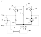
- Embodiment 2 FIG. In the first embodiment, the power conversion device using the half-bridge converter cell has been described. In the second embodiment, a case will be described in which a full-bridge converter cell including two legs each having two upper and lower arms is used.
- FIG. 11 shows an example of the converter cell in the second embodiment.
- the converter cell 10 has a full bridge configuration using four or more semiconductor elements.
- a series body of the semiconductor elements 21 and 22 is connected in parallel with the energy storage element ES, and a connection point between the semiconductor elements 21 and 22 includes an output terminal Po of the converter cell.
- a first bypass element BP1 is provided in parallel with the semiconductor element 22.
- the serial body of the semiconductor elements 23 and 24 is connected in parallel with the energy storage element ES, and the connection point between the semiconductor elements 23 and 24 includes the output terminal No of the converter cell.
- a second bypass element BP ⁇ b> 2 is provided in parallel with the semiconductor element 24.
- FIG. 11B a series body of semiconductor elements 31 and 32 is connected in parallel with the energy storage element ES, and the connection point between the semiconductor elements 31 and 32 is the output terminal Po of the converter cell. Is provided.
- a first bypass element BP ⁇ b> 1 is provided in parallel with the semiconductor element 31.
- a series body of the semiconductor elements 33 and 34 is connected in parallel with the energy storage element ES, and a connection point between the semiconductor elements 33 and 34 includes an output terminal No of the converter cell.
- a second bypass element BP2 is provided in parallel with the semiconductor element 33.
- FIG. 11C further includes components of a failure detector 30 for detecting an abnormality of the bypass element and a gate driving unit 40 for driving the semiconductor element.
- the upper and lower arms are respectively composed of semiconductor elements 21, 22, 23, 24, to which an energy storage element ES and a bypass element BP are connected as shown in the figure.
- a capacitor is used for the energy storage element ES.
- the bypass element BP for example, a mechanical switch such as a vacuum switch or a semiconductor switch constituted by a semiconductor element is used.
- the semiconductor elements 21, 22, 23, and 24 are composed of switching elements 21s, 22s, 23s, and 24s, and diode elements 21d, 22d, 23d, and 24d connected in antiparallel to each.
- an IGBT Insulated-Gate Bipolar Transistor
- GCT Gate Commutated Turn-off thyristor
- MOSFET Metal-Oxide-Semiconductor Field-Effect Transistor switching element
- Each of these arms may have a structure in which a plurality of semiconductor elements are connected in parallel according to the current capacity, or a structure in which a plurality of semiconductor elements are connected in series according to the voltage tolerance. It is good.
- the output terminal Po of the converter cell 10 is provided at the connection point of the semiconductor elements 21 and 22, and the output terminal No. of the converter cell 10 is provided at the connection point of the semiconductor elements 23 and 24.
- Each of the switching elements 21 s to 24 s is on / off controlled based on the gate drive signal from the gate drive unit 40. Then, the switching elements 21 s to 24 s are turned on / off to convert power between the pair of output terminals Po and No and the energy storage element ES, whereby energy is stored between the output terminals of the converter cell 10. Either a positive voltage across the element ES, a negative voltage across the energy storage element ES, or a zero voltage can be output.
- Non-Patent Document 1 a converter cell constituted by a so-called half-bridge having only one leg in the converter cell is used.
- the half-bridge converter cell can produce only two output voltages, either positive voltage across the energy storage element ES or zero voltage.
- Non-Patent Document 2 since it is configured by a full bridge including two legs, a negative voltage of the energy storage element ES can be output, and the degree of freedom of control is improved.
- the converter cell 10 configured as a full bridge shown in FIG. 11 (c) will be described as an object, but protection of the converter cell, which is a main part of the present invention, at the time of abnormality is described. About the structure of a part, it is applicable similarly also in the case of the converter cell comprised by the half bridge.
- a failure detector 30 is provided, and any one of the converter cells 10 is abnormal (for example, a failure of a semiconductor element or a gate drive unit 40 that sends a gate drive signal to a switching element). Is detected), the bypass element BP of the converter cell 10 in which the abnormality is detected is closed, and the converter cell 10 is bypassed.
- Redundant design for example, 1 cell
- a margin in the number of series of converter cells 10 so that an operation equivalent to a steady operation (power conversion operation when no abnormality occurs in the converter cell 10) is possible. If any one of the converter cells 10 becomes abnormal, it is possible to continuously perform the power conversion operation by bypassing the converter cell 10. .
- bypass element BP may be exposed to harsh conditions with its closing operation, and if it is damaged due to this harsh use, it cannot perform a reliable opening / closing operation thereafter. The continuation of operation as a power converter cannot be compensated.
- These converter cells should select and output three output voltages: a positive energy storage element voltage, a negative energy storage element voltage, and a zero voltage compared to a half-bridge converter cell. The degree of freedom of control is improved.
- FIG. 12 shows a power converter in which a plurality of converter cells 10 are connected in series and connected in a star connection form, and is called a star connection cascade converter or the like.
- FIG. 13 shows a power conversion apparatus in which a plurality of converter cells 10 are connected in series and connected in a delta connection form, which is called a delta connection cascade converter.
- 401 is a reactor.
- a known technique can be used for the control of the steady operation (power conversion operation when no abnormality occurs in the converter cell) in FIGS. 12 and 13.
- Non-Patent Document 3 and Non-Patent Document 4 can be used, and detailed description thereof is omitted here.
- a case where the bypass element BP1 or BP2 is closed in a state where a semiconductor element to which the bypass elements BP1 and BP2 are not connected in parallel is short-circuited can be considered.
- the semiconductor elements 22, 24, 31, and 33 connected in parallel with the bypass element to be closed are turned on simultaneously or first so that the bypass element To prevent damage.
- FIG. 1 Specifically, in FIG. 1
- the control power means a power supplied to a gate driver for turning on / off a semiconductor element or a power supplied to a control board that determines on / off logic.
- a method for detecting this abnormality there is a method in which the voltage of the control power supply is detected and a comparator (comparator) determines whether or not the voltage is within the normal operating range. An abnormality can be detected using this method.
- a control voltage is supplied to a control terminal (not shown) or a control coil (not shown) of the bypass element BP.
- the case is closed due to malfunction due to noise of the bypass element BP1 or BP2.
- the failure detector 30 detects an abnormality of the converter cell 10 and the bypass element BP is closed based on this, so to speak, the bypass element.
- the BP is the normal normal closing operation.
- the energy storage element ES This is a case where a very excessive current flows to the closed bypass element BP through the short-circuited semiconductor element due to the energy charges charged in the circuit, and the bypass element BP may be damaged by the excessive current. .
- the second case is a case where the bypass element BP is closed in a state where the failure detector 30 has not detected an abnormality of the converter cell 10, that is, the bypass element BP is closed due to a malfunction.
- the bypass element BP is closed in a state where the failure detector 30 has not detected an abnormality of the converter cell 10, that is, the bypass element BP is closed due to a malfunction.
- a discharge current flows to the bypass element BP that is closed due to the malfunction via the semiconductor element that is in the ON state at this time. If this is left unattended, the semiconductor element develops into a short-circuited state, and this is accompanied by a sudden increase in the discharge current, which may damage the bypass element BP.
- the failure detector 30 detects general abnormality of the converter cell 10 that is assumed.
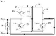
- the thick line arrows in FIG. 14C indicate that the semiconductor elements 21 and 24 in the short-circuit state flow from the energy storage element ES that flows when the bypass element BP is closed when the semiconductor elements 21 and 24 at the diagonal positions are in the short-circuit state.
- the short circuit current which flows into bypass element BP via 24 is shown.
- the bypass element BP is designed with a current value flowing through the converter cell 10 during a normal power conversion operation. Usually, this current is several kA or less. On the other hand, the short-circuit current described above reaches several tens to several hundreds kA. Therefore, there is a possibility that the closed bypass element BP may be damaged by this short-circuit current. In this case, the power conversion device cannot continuously perform the power conversion operation. In other words, reliability decreases. The same applies when the semiconductor elements 22 and 23 at the diagonal positions are short-circuited.
- the failure detector 30 detects an abnormality of the converter cell 10, it is assumed that the semiconductor element is in the above-described short-circuit state, and the most severe state may occur as the bypass element BP to be closed. Therefore, in the present invention, the switching elements 21s and 23s of the upper arm are turned on at the same time or before the bypass element BP is closed. By controlling the switching elements 21s and 23s of the upper arm to be in an on state, the output terminals Po and No are short-circuited by a semiconductor element. As a result, in parallel with the bypass element BP, another current path not including this bypass element BP (from P 0 through N 0 , passing through the switching elements 21 s and 23 s, which is named N in FIG. 14C), is reached. A dotted path) is formed. Since the semiconductor element 21 in the short-circuit state is already in the on state, only the switching element 23s that is not in failure is controlled to be substantially on.
- the semiconductor elements 23 and 24 are turned on or short-circuited, and the energy storage element ES is short-circuited and discharged through the semiconductor elements 23 and 24.
- the semiconductor element is sacrificed before the bypass element BP and is protected from overcurrent.
- the energy storage element ES is short-circuited via the semiconductor element by controlling the switching element so that the output terminals Po and No are short-circuited via the semiconductor element.
- a mechanical switch such as a vacuum switch generally requires several ms or more, whereas the switching element takes several ⁇ s. Can be on. That is, it is relatively easy to make the closing response time from the closing command to the actual closing in the bypass element BP longer than the on response time from the on command to the actual turning on in the switching element. Thus, it is relatively easy to turn on the semiconductor elements 21 and 23 before the bypass element BP is closed.
- the switching elements 21 s and 23 s of the upper arm are turned on.
- this is based on the assumption that a second case, which will be described later, assumes a protective operation for turning off the switching elements with the same device.
- the protection operation to be turned on is performed by the upper arm element and the protection operation to be turned off by the lower arm element. Therefore, the protection operation for turning the former on may be performed by the lower arm element, and the protection operation for turning the latter off may be performed by the upper arm element.
- the protective operation for turning the former on it may be carried by the elements of the upper and lower arms. In this case, since the discharge current flowing from the energy storage element ES to the semiconductor element is divided into two circuits, the current flowing into each semiconductor element is reduced.
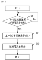
- FIG. 15 shows a flowchart of the protection operation of the bypass element.
- it is determined whether or not the converter cell 10 is abnormal by the failure detector 30 (step S1). If it is abnormal (Yes in step S1), the converter cell 10 needs to be bypassed. A close command is given to the element BP, and an on command is given to the switching elements 21s and 23s of the upper arm (step S2). By performing such processing, the switching elements 21s and 23s of the upper arm are turned on (step S3), and at the same time or after that, the bypass element BP is closed (step S4).
- FIG. 16 is a flowchart in the case where the above-described protection operation for turning on the state is performed by the lower arm element.
- the protection operation for turning on the switching element described in FIG. 15 is bypassed regardless of the type of the detected abnormal event.
- the operation is performed assuming the first case described above, which is the most severe for the element BP, and the bypass element BP is surely prevented from being damaged.
- the protective operation of short-circuiting between the output terminals Po and No by the semiconductor element at the time of failure detection is that the abnormality detected by the failure detector 30 is not a short-circuit failure of the semiconductor element but another type in the converter cell 10. Even an abnormal event can be applied. That is, when the failure is not a short-circuit failure of the semiconductor element but another type of abnormal event in the converter cell 10, the switching elements 21s and 23s of the upper arm are controlled to be turned on between the output terminals Po and No. Even if a short circuit occurs, there is no path through which the energy storage element ES is short-circuited, so that the energy charge charged in the energy storage element ES is not consumed. On the other hand, since the semiconductor element short-circuits the output terminals Po and No prior to the bypass element BP, it is possible to quickly enter the bypass state. Therefore, the operation of the power conversion device can be continued more reliably.
- FIG. 17 employs a failure detector 30 that can detect abnormalities in the converter cell 10 by distinguishing between short-circuit faults of semiconductor elements and other faults. It is a flowchart which shows the protection operation
- step S1 it is determined whether or not the converter cell 10 is abnormal by the failure detector 30 (step S1). If it is abnormal (Yes in step S1), it is further determined whether or not there is a short circuit failure of the semiconductor element. A determination is made (step S5). In the case of a short circuit failure of the semiconductor element (Yes in step S5), a close command is given to the bypass element BP, and an on command is given to the switching elements 21s and 23s of the upper arm (step S2). By performing such processing, the switching elements 21s and 23s of the upper arm are turned on (step S3), and at the same time or after that, the bypass element BP is closed (step S4).
- step S5 When it is determined in step S5 that the detected failure is not a short-circuit failure of the semiconductor element (No in step S5), only the closing command is given to the bypass element BP (step S6), and the switching element is turned on. Is not commanded, the bypass element BP is closed (step S7).
- step S6 When it is determined in step S5 that the detected failure is not a short-circuit failure of the semiconductor element (No in step S5), only the closing command is given to the bypass element BP (step S6), and the switching element is turned on. Is not commanded, the bypass element BP is closed (step S7).
- the abnormality detected by the failure detector 30 in the operation of turning on the switching element at the same time or before the bypass element BP is closed is due to a short circuit failure of the semiconductor element. Since the operation is sometimes limited, the frequency of the protection operation for turning on the switching element can be minimized, and the portion related to the protection control can be reduced in size.
- FIGS. 18 and 19 Next, another second case set as a severe condition for the bypass element BP will be described with reference to FIGS. 18 and 19.
- the failure detector 30 detects general abnormality of the converter cell 10 that is assumed.
- the failure detector 30 is not detecting an abnormality. That is, this is a case where the bypass element BP is closed due to a malfunction.
- the semiconductor elements 21 and 24 controlled to be in the on state are illustrated by solid lines, and the semiconductor elements 22 and 23 controlled to be in the off state are illustrated by dotted lines.
- the energy storage element ES is short-circuited between the closed bypass element BP and the semiconductor elements 21 and 24 in the on state.
- the short circuit current is limited to a value called a saturation current (usually about several kA).
- the semiconductor element generally fails in several tens of ⁇ s and becomes a complete short-circuit state, and the current of the bypass element BP increases from several tens kA to several hundreds kA at that time. As a result, the bypass element BP may be damaged.
- an arm short-circuit protection unit is provided in the gate drive unit 40 that drives the switching elements 22s and 24s of the lower arm.
- the arm short-circuit protection unit means a current sensor indicated by 502A, 502B, etc. in FIG. 18, an overcurrent detector that detects an overcurrent of a semiconductor element from a detection output of the current sensor, and detects this overcurrent.
- the bypass element BP that is closed due to malfunction and the drive unit that releases the short-circuit state of the energy storage element ES formed through the semiconductor elements 21 and 24 are referred to. Yes.
- the “arm short circuit protection unit” is described.
- the “load short circuit protection unit” may be described as a part that protects the element from a short circuit outside the output terminal.
- the term “arm short-circuit protection part” is used as a general term for parts that protect a semiconductor element from a short-circuit current.
- the arm short-circuit protection unit directly or indirectly detects that a short-circuit current has flowed through the semiconductor element, and blocks the switching elements 22s and 24s of the lower arm. Therefore, the current sensor may be connected to both ends of the energy storage element ES and the semiconductor elements 21 and 23 as in the current sensor 501 shown in FIG. 7, or the lower arm semiconductor as in the current sensors 502A and 502B. In the case of the elements 22 and 24, or in the case of a module type element, they may be incorporated in the semiconductor elements 22 and 24. Moreover, you may connect to the connection part of a semiconductor element and the bypass element BP like the current sensor 503. FIG.
- the switching elements 22s and 24s of the lower arm are turned off, but this is based on the first device, and the protective operation for turning on the switching elements is adopted in the same device.
- the protection operation to be turned on is performed by the upper arm element
- the protection operation to be turned off is performed by the lower arm element. Therefore, the protection operation for turning the former on may be performed by the lower arm element, and the protection operation for turning the latter off may be performed by the upper arm element.
- the latter protective operation for turning off it may be carried by the elements of the upper and lower arms.
- FIG. 19 shows a flowchart of the above protection operation.
- the arm short circuit protection unit detects an overcurrent in a state where the failure detector 30 has not detected an abnormality of the converter cell 10 (Yes in step S8)
- the lower arm switching elements 22s and 24s are turned off.
- a command is given to turn off the switching elements 22s and 24s (step S9).
- the short circuit current is removed (step S10).
- the switching element is turned off within several tens of microseconds until the semiconductor element fails, so that the short-circuit state of the energy storage element ES can be released and the short-circuit current can be removed.
- the high-voltage semiconductor element used in the circuit as shown in FIG. 1 generally has a withstand characteristic (non-breaking characteristic) with respect to the short-circuit current within 10 ⁇ s, so that a short circuit occurs. Then, it can be reliably protected by shutting off within 10 ⁇ s. By this protection operation, the semiconductor element does not break down, so that it is possible to prevent a current of several tens kA to several hundreds kA from flowing through the bypass element BP. Therefore, failure of the bypass element BP can be prevented.
- an operation called “soft cut-off” may be performed by a switching operation slower than the switching operation in the case of normal control. This is because the saturation current of the semiconductor element is larger than the normally controlled current, so that the surge voltage generated at both ends of the semiconductor element at the time of interruption is suppressed.
- FIG. 10 is a circuit diagram in which the main points are extracted from the publication.
- a detection unit 511 that detects a short-circuit current and a blocking unit 512 that performs a blocking operation when a short-circuit current is detected are shown for the target semiconductor element 510.
- the detection unit 511 that detects a short-circuit current detects whether the collector potential is equal to or higher than a predetermined voltage when the semiconductor element 510 has an ON signal. At the time of a short circuit, the voltage of the energy storage element ES is applied to both ends of the semiconductor element, and the on-state voltage increases. On the other hand, when not in a short-circuit state, the voltage drop of the semiconductor element is several volts. The detection unit 511 determines whether or not a short-circuit current is flowing by detecting the collector potential and comparing it with a comparator.
- the blocking unit 512 receives a signal from the detection unit 511 and blocks it.
- an operation called “soft interruption” is realized by performing the interruption through a larger resistance than at the time of interruption of the steady operation.
- the switching element of the lower arm is turned off to remove the short-circuit current when an overcurrent of the semiconductor element is detected in the state where the abnormality of the converter cell 10 is not detected.
- unnecessary protection operation is suppressed within a range that does not affect the protection of the bypass element BP.
- the requirement for overcurrent detection may not be imposed.
- step S11 when it is detected that the bypass element BP is closed while the failure detector 30 has not detected an abnormality of the converter cell 10 (Yes in step S11), the switching element 22s of the lower arm is detected. , 24s is given an off command, and the switching elements 22s, 24s are turned off (step S9). Thereby, the short circuit state of the energy storage element ES formed via the closed bypass element BP and the semiconductor element is released (step S12).
- the closing operation of the bypass element BP can be detected by detecting the voltage across the bypass element BP or by monitoring the auxiliary contact that performs the same opening / closing operation as the main contact of the bypass element BP. In this case, the frequency of the protection operation for turning off the switching element is increased, but the configuration operation of the protection circuit can be simplified while the bypass element BP is reliably protected.
- the converter cell is configured by a full bridge. Therefore, when an abnormality is detected in the converter cell, both bypass elements BP1 and BP2 are closed. . At that time, the semiconductor elements connected in parallel with them are also turned on at the same time or earlier. By doing so, the converter cell in which an abnormality has occurred can be reliably bypassed. Further, the frequency of the protection operation for turning on the switching element can be kept to a minimum, and the portion related to protection control can be reduced in size.
- FIG. FIG. 22 is a circuit diagram showing an internal configuration example of converter cell 10B used in the power conversion device according to Embodiment 3 of the present invention.
- the switching elements and the diode elements are used for all the semiconductor elements of the converter cell 10.
- one of the two legs The difference is that the semiconductor element of the lower arm is composed of only a diode element.
- this difference will be mainly described.
- Each arm of the converter cell 10B is composed of semiconductor elements 21, 22B, 23, and 24, respectively, to which an energy storage element ES and a bypass element BP are connected as shown in the figure.
- the semiconductor element 22B is composed only of a diode element, and the other three arms are switching elements 21s, 23s, and 24s, and diode elements 21d, 23d, and 24d connected in antiparallel to each of them. It consists of
- the output terminal Po of the converter cell 10B is provided at the connection point of the semiconductor elements 21 and 22B, and the output terminal No. of the converter cell 10B is provided at the connection point of the semiconductor elements 23 and 24.
- the switching elements 21 s, 23 s, and 24 s are on / off controlled based on the gate drive signal from the gate drive unit 40.
- the semiconductor element 22B can be turned on, so that either of the negative voltages at both ends of the energy storage element ES can be output. it can.
- the converter cell 10B of FIG. 22 is inferior in controllability compared to the converter cell 10 of FIG. 11C, but can realize the steady operation disclosed in the previous Non-Patent Document 1. Furthermore, since the number of switching elements is small compared to the converter cell 10 of FIG. 11C, a small and inexpensive power conversion device can be realized.
- the bypass element BP has a short-circuited state of the semiconductor elements 21 and 24 at the diagonal positions as shown in FIG. 23, for example, and the failure detector 30 detects this.
- the first embodiment there is a possibility of being exposed to the harsh conditions described as the first case and the second case. In this harsh condition, A protective operation is required so that the bypass element BP is not damaged.
- the power conversion device according to the second embodiment is similar to that described in the first embodiment when the abnormality of the converter cell occurs.
- the bypass element that closes the output terminal is reliably prevented from being damaged due to the closing operation, and the operation can be continued.
- the advantage is that the apparatus is smaller and less expensive than the case of the first embodiment. There is.
- FIG. FIG. 24 is a circuit diagram showing an example of the internal configuration of converter cell 10C used in the power conversion device according to Embodiment 4 of the present invention.
- the switching elements and the diode elements are used for all the semiconductor elements of the converter cell 10.
- the upper arm of one leg out of the two legs is used for all the semiconductor elements of the converter cell 10.
- these semiconductor elements are composed of only diode elements.
- this difference will be mainly described.
- Each arm of the converter cell 10C is composed of semiconductor elements 21, 22, 23B, and 24, and an energy storage element ES and a bypass element BP are connected to them as shown in the figure.
- the semiconductor element 23B is composed only of diode elements, and the other three arms are switching elements 21s, 23s, 24s and diode elements 21d, 23d, 24d connected in antiparallel to each of them. It consists of
- the output terminal Po of the converter cell 10C is provided at the connection point of the semiconductor elements 21 and 22, and the output terminal No. of the converter cell 10C is provided at the connection point of the semiconductor elements 23B and 24.
- Each switching element 21 s, 22 s, 24 s is on / off controlled based on a gate drive signal from the gate drive unit 40.
- the semiconductor element 23B can be turned on, so that either of the negative voltages at both ends of the energy storage element ES can be output. it can.
- the converter cell 10C of FIG. 24 is inferior in controllability compared to the converter cell 10 of FIG. 11C, but since the number of switching elements is small, a small and inexpensive power conversion device can be realized.
- the bypass element BP has, for example, the semiconductor elements 21 and 24 at the diagonal positions short-circuited as shown in FIG. 25, and the failure detector 30 detects this.
- the first embodiment there is a possibility of being exposed to the harsh conditions described as the first case and the second case. In this harsh condition, A protective operation is required so that the bypass element BP is not damaged.
- the details of these protection operations are as described in the first embodiment, and a description thereof will be omitted.
- the switching element to be turned on may be, for example, FIG. In this case, it is limited to the switching element 22s of the lower arm.
- the power conversion device is the same as that described in the first and second embodiments, when a converter cell abnormality occurs.
- the bypass element that closes the output terminal is reliably prevented from being damaged due to the closing operation, and the operation can be continued, and the apparatus is smaller than those in the first and second embodiments. There is an advantage that it is inexpensive.
- BP, BP1, BP2 Bypass element ES energy storage element, P, N DC terminal, Po, No Cell output terminal, U, V, W AC terminal, 10, 10B, 10C Converter cell, 21, 22, 22B, 23, 23B, 24, 31, 32, 33, 34 Semiconductor element, 21s, 22s, 23s, 24s, 31s, 32s, 33s, 34s Switching element, 21d 22d, 23d, 24d, 31d, 32d, 33d, 34d Diode element, 30 Fault detector, 40 Gate drive, 301P, 301N, 301, 401 Reactor, 501, 502, 502A, 502B, 503, 601, 602, 603 Current sensor.
Landscapes
- Engineering & Computer Science (AREA)
- Power Engineering (AREA)
- Inverter Devices (AREA)
Abstract
Priority Applications (4)
| Application Number | Priority Date | Filing Date | Title |
|---|---|---|---|
| EP15758979.7A EP3116118B1 (fr) | 2014-03-05 | 2015-02-26 | Dispositif de conversion de puissance |
| EP20184430.5A EP3745581B1 (fr) | 2014-03-05 | 2015-02-26 | Dispositif de conversion d'alimentation électrique |
| US15/120,683 US10186952B2 (en) | 2014-03-05 | 2015-02-26 | Power conversion device |
| JP2015551916A JP5889498B2 (ja) | 2014-03-05 | 2015-02-26 | 電力変換装置 |
Applications Claiming Priority (4)
| Application Number | Priority Date | Filing Date | Title |
|---|---|---|---|
| JP2014042394 | 2014-03-05 | ||
| JP2014-042394 | 2014-03-05 | ||
| JP2014103939 | 2014-05-20 | ||
| JP2014-103939 | 2014-05-20 |
Publications (1)
| Publication Number | Publication Date |
|---|---|
| WO2015133365A1 true WO2015133365A1 (fr) | 2015-09-11 |
Family
ID=54055174
Family Applications (1)
| Application Number | Title | Priority Date | Filing Date |
|---|---|---|---|
| PCT/JP2015/055655 Ceased WO2015133365A1 (fr) | 2014-03-05 | 2015-02-26 | Dispositif de conversion de puissance |
Country Status (4)
| Country | Link |
|---|---|
| US (1) | US10186952B2 (fr) |
| EP (2) | EP3745581B1 (fr) |
| JP (1) | JP5889498B2 (fr) |
| WO (1) | WO2015133365A1 (fr) |
Cited By (7)
| Publication number | Priority date | Publication date | Assignee | Title |
|---|---|---|---|---|
| WO2017152989A1 (fr) * | 2016-03-11 | 2017-09-14 | Siemens Aktiengesellschaft | Système comprenant un module d'un convertisseur, et un commutateur |
| WO2017203865A1 (fr) * | 2016-05-25 | 2017-11-30 | 三菱電機株式会社 | Convertisseur électrique |
| WO2018001515A1 (fr) * | 2016-07-01 | 2018-01-04 | Abb Schweiz Ag | Détection de dérivées temporelles de courant élevé dans une cellule d'un convertisseur modulaire à plusieurs niveaux |
| JP6359213B1 (ja) * | 2017-06-27 | 2018-07-18 | 三菱電機株式会社 | 電力変換装置 |
| US20190238050A1 (en) * | 2016-09-16 | 2019-08-01 | Mitsubishi Electric Corporation | Power conversion device |
| JP6563163B1 (ja) * | 2019-03-01 | 2019-08-21 | 三菱電機株式会社 | 電力変換装置 |
| JP6689472B1 (ja) * | 2019-06-12 | 2020-04-28 | 三菱電機株式会社 | 電力変換装置 |
Families Citing this family (18)
| Publication number | Priority date | Publication date | Assignee | Title |
|---|---|---|---|---|
| WO2016002319A1 (fr) * | 2014-06-30 | 2016-01-07 | 三菱電機株式会社 | Dispositif de conversion de puissance |
| EP2996215A1 (fr) * | 2014-09-11 | 2016-03-16 | Alstom Technology Ltd | Convertisseur de source de tension |
| JP6227192B2 (ja) * | 2015-03-17 | 2017-11-08 | 三菱電機株式会社 | 電力変換装置 |
| CN208433908U (zh) * | 2015-05-28 | 2019-01-25 | 西门子公司 | 电压源换流器模块和换流器 |
| CN108702083B (zh) * | 2016-02-12 | 2020-09-18 | Abb电网瑞士股份公司 | 用于hvdc功率站的转换器模块 |
| CN107689739A (zh) * | 2016-08-05 | 2018-02-13 | 南京南瑞继保电气有限公司 | 一种可重构mmc子模块单元及其控制单元 |
| ES2812876T3 (es) * | 2016-09-05 | 2021-03-18 | Siemens Energy Global Gmbh & Co Kg | Procedimiento para la descarga de un acumulador de energía eléctrica |
| WO2018145724A1 (fr) * | 2017-02-07 | 2018-08-16 | Abb Schweiz Ag | Système de circuit de protection |
| PL3602087T3 (pl) | 2017-04-20 | 2025-07-07 | Abb Schweiz Ag | Wykrywanie zdarzenia zwarcia w przetworniku elektrycznym |
| KR101943884B1 (ko) * | 2017-06-02 | 2019-01-30 | 효성중공업 주식회사 | Mmc 컨버터 및 그의 서브모듈 |
| KR101943885B1 (ko) * | 2017-06-02 | 2019-01-30 | 효성중공업 주식회사 | Mmc 컨버터 및 그의 서브모듈 |
| CN110999054B (zh) * | 2017-08-09 | 2023-03-31 | 西门子能源全球有限公司 | 用于变流器的功率模块和多电平变流器 |
| JP6770559B2 (ja) * | 2018-08-29 | 2020-10-14 | 株式会社Subaru | 電力変換装置および車両 |
| EP3621193B1 (fr) * | 2018-09-06 | 2025-10-29 | Hitachi Energy Ltd | Fonction de mode de défaillance de court-circuit stable artificiel à l'aide de modules parallèles pour chaque fonction de commutation |
| JP6559387B1 (ja) * | 2018-12-25 | 2019-08-14 | 三菱電機株式会社 | 電力変換装置 |
| US10700617B1 (en) * | 2019-09-06 | 2020-06-30 | ABBSchweiz AG | Boosting modular multilevel converter |
| WO2021181583A1 (fr) * | 2020-03-11 | 2021-09-16 | 三菱電機株式会社 | Dispositif de conversion de puissance |
| WO2022037783A1 (fr) * | 2020-08-20 | 2022-02-24 | Hitachi Energy Switzerland Ag | Gestion de défauts dans une cellule |
Citations (5)
| Publication number | Priority date | Publication date | Assignee | Title |
|---|---|---|---|---|
| JPH09191662A (ja) * | 1996-01-10 | 1997-07-22 | Fuji Electric Co Ltd | 半導体装置の保護方法 |
| JP2000049581A (ja) * | 1998-07-27 | 2000-02-18 | Hitachi Ltd | 半導体電力変換装置 |
| JP2010512135A (ja) * | 2006-12-08 | 2010-04-15 | シーメンス アクチエンゲゼルシヤフト | 電圧形インバータの直流側短絡を制御するための半導体保護素子 |
| JP2013027260A (ja) * | 2011-07-26 | 2013-02-04 | Hitachi Ltd | 電力変換装置 |
| JP2013169088A (ja) * | 2012-02-16 | 2013-08-29 | Hitachi Ltd | 電力変換装置、直流変電所、直流送電システム及び電力変換装置の制御方法 |
Family Cites Families (16)
| Publication number | Priority date | Publication date | Assignee | Title |
|---|---|---|---|---|
| KR0171713B1 (ko) | 1995-12-12 | 1999-05-01 | 이형도 | 전력용 반도체 트랜지스터의 과전류 보호회로 |
| FR2794890B1 (fr) * | 1999-06-08 | 2001-08-10 | Crouzet Automatismes | Relais electromecanique assiste a la commutation par semi-conducteur |
| DE102005040543A1 (de) * | 2005-08-26 | 2007-03-01 | Siemens Ag | Stromrichterschaltung mit verteilten Energiespeichern |
| DE102007018344B4 (de) | 2007-04-16 | 2022-08-04 | Siemens Energy Global GmbH & Co. KG | Vorrichtung zum Schutz von Umrichtermodulen |
| EP2406873B1 (fr) * | 2009-03-11 | 2019-08-14 | ABB Schweiz AG | Convertisseur de source de tension modulaire |
| EP2443733A1 (fr) * | 2009-06-15 | 2012-04-25 | Alstom Grid UK Limited | Commande de convertisseur |
| JP5315155B2 (ja) * | 2009-07-23 | 2013-10-16 | 日立オートモティブシステムズ株式会社 | 半導体素子制御装置、車載用電機システム |
| AU2010348910B2 (en) * | 2010-03-18 | 2015-12-03 | Abb Research Ltd | Converter cell for cascaded converters, control system and method for bypassing a faulty converter cell |
| EP2369725B1 (fr) * | 2010-03-25 | 2012-09-26 | ABB Schweiz AG | Dispositif de court-circuit |
| CN103036415B (zh) * | 2011-09-29 | 2015-07-08 | 台达电子企业管理(上海)有限公司 | 一种功率半导体开关串联电路及其控制方法 |
| WO2013064310A1 (fr) * | 2011-11-03 | 2013-05-10 | Abb Technology Ag | Circuit convertisseur et procédé permettant de faire fonctionner un tel circuit convertisseur |
| KR101389579B1 (ko) * | 2012-12-28 | 2014-04-29 | 주식회사 효성 | 전력용 컨버터 |
| US9716425B2 (en) * | 2013-01-21 | 2017-07-25 | Abb Schweiz Ag | Multilevel converter with hybrid full-bridge cells |
| CN103280989B (zh) * | 2013-05-15 | 2017-02-08 | 南京南瑞继保电气有限公司 | 一种换流器及其控制方法 |
| WO2015098146A1 (fr) * | 2013-12-24 | 2015-07-02 | 三菱電機株式会社 | Dispositif de conversion de puissance |
| JP5622978B1 (ja) * | 2014-02-14 | 2014-11-12 | 三菱電機株式会社 | 直流送電系統の保護システムおよび交流直流変換器ならびに直流送電系統の遮断方法 |
-
2015
- 2015-02-26 WO PCT/JP2015/055655 patent/WO2015133365A1/fr not_active Ceased
- 2015-02-26 EP EP20184430.5A patent/EP3745581B1/fr active Active
- 2015-02-26 EP EP15758979.7A patent/EP3116118B1/fr active Active
- 2015-02-26 US US15/120,683 patent/US10186952B2/en active Active
- 2015-02-26 JP JP2015551916A patent/JP5889498B2/ja active Active
Patent Citations (5)
| Publication number | Priority date | Publication date | Assignee | Title |
|---|---|---|---|---|
| JPH09191662A (ja) * | 1996-01-10 | 1997-07-22 | Fuji Electric Co Ltd | 半導体装置の保護方法 |
| JP2000049581A (ja) * | 1998-07-27 | 2000-02-18 | Hitachi Ltd | 半導体電力変換装置 |
| JP2010512135A (ja) * | 2006-12-08 | 2010-04-15 | シーメンス アクチエンゲゼルシヤフト | 電圧形インバータの直流側短絡を制御するための半導体保護素子 |
| JP2013027260A (ja) * | 2011-07-26 | 2013-02-04 | Hitachi Ltd | 電力変換装置 |
| JP2013169088A (ja) * | 2012-02-16 | 2013-08-29 | Hitachi Ltd | 電力変換装置、直流変電所、直流送電システム及び電力変換装置の制御方法 |
Non-Patent Citations (1)
| Title |
|---|
| See also references of EP3116118A4 * |
Cited By (18)
| Publication number | Priority date | Publication date | Assignee | Title |
|---|---|---|---|---|
| EP3417534A1 (fr) * | 2016-03-11 | 2018-12-26 | Siemens Aktiengesellschaft | Système comprenant un module d'un convertisseur, et un commutateur |
| EP3417534B1 (fr) * | 2016-03-11 | 2025-07-16 | Siemens Energy Global GmbH & Co. KG | Convertisseur modulaire multiniveaux |
| WO2017152989A1 (fr) * | 2016-03-11 | 2017-09-14 | Siemens Aktiengesellschaft | Système comprenant un module d'un convertisseur, et un commutateur |
| US10468972B2 (en) | 2016-05-25 | 2019-11-05 | Mitsubishi Electric Corporation | Power converter including a plurality of converter cells connected in multiple series |
| JP6275352B1 (ja) * | 2016-05-25 | 2018-02-07 | 三菱電機株式会社 | 電力変換装置 |
| WO2017203865A1 (fr) * | 2016-05-25 | 2017-11-30 | 三菱電機株式会社 | Convertisseur électrique |
| EP3468026B1 (fr) * | 2016-05-25 | 2024-11-27 | Mitsubishi Electric Corporation | Convertisseur électrique |
| WO2018001515A1 (fr) * | 2016-07-01 | 2018-01-04 | Abb Schweiz Ag | Détection de dérivées temporelles de courant élevé dans une cellule d'un convertisseur modulaire à plusieurs niveaux |
| US20190238050A1 (en) * | 2016-09-16 | 2019-08-01 | Mitsubishi Electric Corporation | Power conversion device |
| US10530243B2 (en) * | 2016-09-16 | 2020-01-07 | Mitsubishi Electric Corporation | Power conversion device with malfunction detection |
| JP6359213B1 (ja) * | 2017-06-27 | 2018-07-18 | 三菱電機株式会社 | 電力変換装置 |
| WO2019003290A1 (fr) * | 2017-06-27 | 2019-01-03 | 三菱電機株式会社 | Dispositif de conversion de puissance |
| US10992219B2 (en) | 2017-06-27 | 2021-04-27 | Mitsubishi Electric Corporation | Power conversion device |
| JP6563163B1 (ja) * | 2019-03-01 | 2019-08-21 | 三菱電機株式会社 | 電力変換装置 |
| WO2020178877A1 (fr) * | 2019-03-01 | 2020-09-10 | 三菱電機株式会社 | Dispositif de conversion de puissance |
| WO2020250358A1 (fr) | 2019-06-12 | 2020-12-17 | 三菱電機株式会社 | Dispositif de conversion de puissance |
| US11909307B2 (en) | 2019-06-12 | 2024-02-20 | Mitsubishi Electric Corporation | Power conversion device |
| JP6689472B1 (ja) * | 2019-06-12 | 2020-04-28 | 三菱電機株式会社 | 電力変換装置 |
Also Published As
| Publication number | Publication date |
|---|---|
| EP3745581A1 (fr) | 2020-12-02 |
| JP5889498B2 (ja) | 2016-03-22 |
| EP3116118A1 (fr) | 2017-01-11 |
| JPWO2015133365A1 (ja) | 2017-04-06 |
| US20170012521A1 (en) | 2017-01-12 |
| EP3116118B1 (fr) | 2024-07-03 |
| EP3116118A4 (fr) | 2018-03-28 |
| US10186952B2 (en) | 2019-01-22 |
| EP3745581B1 (fr) | 2022-11-30 |
Similar Documents
| Publication | Publication Date | Title |
|---|---|---|
| JP5889498B2 (ja) | 電力変換装置 | |
| CA2563457C (fr) | Controleur a pont inverseur implementant un schema de protection contre les courts-circuits | |
| US10367423B1 (en) | Power conversion device | |
| US10530243B2 (en) | Power conversion device with malfunction detection | |
| WO2011023237A1 (fr) | Module de cellule de conversion, système convertisseur de source de tension comprenant un tel module et procédé de commande d'un tel système | |
| JP6646870B2 (ja) | チョッパ装置 | |
| JP5031607B2 (ja) | 直流高速真空遮断装置 | |
| JP6919486B2 (ja) | 直流遮断装置 | |
| CN114128067B (zh) | 直流配电盘 | |
| JP6455719B2 (ja) | 無停電電源システム | |
| JP7682424B1 (ja) | 電力変換装置 | |
| Hammes et al. | High-inductive short-circuit Type IV in multi-level converter protection schemes | |
| US11855445B2 (en) | Power conversion device | |
| JP7731485B2 (ja) | 電力変換装置 | |
| JP7608029B2 (ja) | 電力変換装置 | |
| JP7414380B2 (ja) | 電力変換装置 | |
| JP7473786B2 (ja) | サージ吸収回路、及び限流回路 | |
| JP2025067140A (ja) | 電力変換装置 | |
| JP2007189756A (ja) | 電力用スイッチング素子の短絡保護装置 | |
| JPH0847182A (ja) | 無停電電源装置の電源切換回路 | |
| HK40067162A (zh) | 直流配电盘 | |
| HK40067162B (zh) | 直流配电盘 | |
| JPH04125057A (ja) | ゲートターンオフサイリスタのゲート駆動装置 |
Legal Events
| Date | Code | Title | Description |
|---|---|---|---|
| ENP | Entry into the national phase |
Ref document number: 2015551916 Country of ref document: JP Kind code of ref document: A |
|
| 121 | Ep: the epo has been informed by wipo that ep was designated in this application |
Ref document number: 15758979 Country of ref document: EP Kind code of ref document: A1 |
|
| WWE | Wipo information: entry into national phase |
Ref document number: 15120683 Country of ref document: US |
|
| REEP | Request for entry into the european phase |
Ref document number: 2015758979 Country of ref document: EP |
|
| WWE | Wipo information: entry into national phase |
Ref document number: 2015758979 Country of ref document: EP |
|
| NENP | Non-entry into the national phase |
Ref country code: DE |