WO2015136579A1 - Écran d'affichage el organique et procédé de fabrication associé - Google Patents
Écran d'affichage el organique et procédé de fabrication associé Download PDFInfo
- Publication number
- WO2015136579A1 WO2015136579A1 PCT/JP2014/003544 JP2014003544W WO2015136579A1 WO 2015136579 A1 WO2015136579 A1 WO 2015136579A1 JP 2014003544 W JP2014003544 W JP 2014003544W WO 2015136579 A1 WO2015136579 A1 WO 2015136579A1
- Authority
- WO
- WIPO (PCT)
- Prior art keywords
- partition
- organic
- width
- partition wall
- groove
- Prior art date
- Legal status (The legal status is an assumption and is not a legal conclusion. Google has not performed a legal analysis and makes no representation as to the accuracy of the status listed.)
- Ceased
Links
Images


Classifications
-
- H—ELECTRICITY
- H10—SEMICONDUCTOR DEVICES; ELECTRIC SOLID-STATE DEVICES NOT OTHERWISE PROVIDED FOR
- H10K—ORGANIC ELECTRIC SOLID-STATE DEVICES
- H10K59/00—Integrated devices, or assemblies of multiple devices, comprising at least one organic light-emitting element covered by group H10K50/00
- H10K59/10—OLED displays
- H10K59/12—Active-matrix OLED [AMOLED] displays
- H10K59/122—Pixel-defining structures or layers, e.g. banks
-
- H—ELECTRICITY
- H10—SEMICONDUCTOR DEVICES; ELECTRIC SOLID-STATE DEVICES NOT OTHERWISE PROVIDED FOR
- H10K—ORGANIC ELECTRIC SOLID-STATE DEVICES
- H10K59/00—Integrated devices, or assemblies of multiple devices, comprising at least one organic light-emitting element covered by group H10K50/00
- H10K59/10—OLED displays
- H10K59/12—Active-matrix OLED [AMOLED] displays
- H10K59/121—Active-matrix OLED [AMOLED] displays characterised by the geometry or disposition of pixel elements
-
- H—ELECTRICITY
- H10—SEMICONDUCTOR DEVICES; ELECTRIC SOLID-STATE DEVICES NOT OTHERWISE PROVIDED FOR
- H10K—ORGANIC ELECTRIC SOLID-STATE DEVICES
- H10K59/00—Integrated devices, or assemblies of multiple devices, comprising at least one organic light-emitting element covered by group H10K50/00
- H10K59/10—OLED displays
- H10K59/12—Active-matrix OLED [AMOLED] displays
- H10K59/1201—Manufacture or treatment
Definitions
- the present invention relates to an organic EL display panel including an organic EL element and a method for manufacturing the same.
- the organic EL element has a pair of electrodes composed of an anode and a cathode, and a light emitting layer sandwiched between the electrodes.
- a hole injection layer, a hole transport layer, or a hole injection / transport layer is disposed between the anode and the light emitting layer as necessary.
- An electron injection layer, an electron transport layer, or an electron injection / transport layer is disposed between the cathode and the light emitting layer as necessary.
- the light emitting layer, hole injection layer, hole transport layer, hole injection / transport layer, electron injection layer, electron transport layer, and electron injection / transport layer each perform their own functions such as light emission, charge injection and transport. These layers are collectively referred to as “functional layers”.
- organic EL element corresponds to each of red, green, and blue sub-pixels.
- a pixel is composed of adjacent red, green, and blue sub-pixels.
- a wet method As a method of manufacturing an organic EL display panel, there is a wet method in which a solution containing a functional material for forming a functional layer is applied to a region where each subpixel is formed on a substrate, and the applied solution is dried. Proposed.
- a partition wall also referred to as a bank
- the solution is generally applied to a recess defined by the partition wall.
- Patent Document 1 discloses a partition having a so-called pixel bank structure (for example, see FIG. 12 of Patent Document 1).
- the pixel bank structure includes a plurality of first partition walls that are long and arranged in parallel, and a plurality of second partition walls that are disposed between adjacent first partition walls.
- a recess is defined by two adjacent first partition walls and two adjacent second partition walls.
- each recess corresponds to a region where a subpixel is formed.
- the amount of solution applied may vary from recess to recess. If the coating amount of the solution varies for each recess, the thickness of the functional layer obtained by drying the solution varies for each subpixel. This causes variations in the light emission characteristics of each subpixel.
- One embodiment of the present invention proposes a technique capable of suppressing variations in the thickness of the functional layer for each subpixel.
- An organic EL display panel includes a pair of first partition walls that are long and spaced apart from each other, and a plurality of the first partition walls are disposed between the pair of first partition walls. In a plurality of recesses defined by the second partition walls, the pair of first partition walls, and the plurality of second partition walls, which are spaced apart from each other in the direction along which the first partition walls are connected. And a functional layer that is disposed and constitutes at least a part of the organic EL element.
- Each of the second partition walls has a groove portion on the upper surface that communicates adjacent recesses across the second partition wall, and the width of the groove portion in a direction perpendicular to the direction along the first partition wall is adjacent to the second partition wall. It is narrower than the width of the recess in the direction perpendicular to the direction along the first partition, and has a dimension of 2 ⁇ m or more and 6 ⁇ m or less.
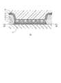
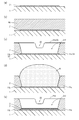
- Partial sectional view of an organic EL display panel according to an embodiment of the present invention
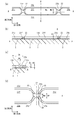
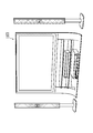
- the perspective view for demonstrating a partition structure (A) is a plan view of the partition wall structure, (b) is a longitudinal sectional view of the partition wall structure, (c) is a transverse sectional view of the partition wall structure, and (d) is an enlarged plan view of the partition wall structure.
- (A) And (b) is a figure for demonstrating the measuring method of the width
- (A) is a plan view of a partition structure when a solution is applied, and (b) is a longitudinal sectional view of the partition structure when a solution is applied.
- (A)-(c) is a figure which shows the mode of the solution of a drying process It is the trace figure of the photograph of the organic electroluminescent display panel obtained by experiment, (a) is a trace figure of the sample whose groove part width is 10 micrometers, (b) is the trace figure of the sample whose groove part width is 4 micrometers.
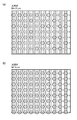
- the figure which shows the result of the experiment which verifies the thickness uniformity of the functional layer The figure for explaining the result of the experiment which verifies the influence to the circumference when the abnormal sub pixel exists (A) to (e) are partial cross-sectional views showing the manufacturing process of the organic EL display panel according to the embodiment of the present invention.
- FIG. 1 is a partial cross-sectional view showing a manufacturing process of an organic EL display panel according to an embodiment of the present invention. It is an enlarged plan view which shows the modification of the shape of a groove part, (a) is a 1st modification, (b) is a 2nd modification. External view of display device Functional block diagram of display device
- An organic EL display panel includes a pair of first partition walls that are long and spaced apart from each other, and a plurality of organic EL display panels are provided between the pair of first partition walls.
- a plurality of partitions defined by a second partition which is disposed in the direction along the one partition, and which connects the pair of first partitions, and the pair of first partitions and the plurality of second partitions.
- a functional layer disposed in each of the recesses and constituting at least a part of the organic EL element.
- Each of the second partition walls has a groove portion on the upper surface that communicates adjacent recesses across the second partition wall, and the width of the groove portion in a direction perpendicular to the direction along the first partition wall is adjacent to the second partition wall. It is narrower than the width of the recess in the direction perpendicular to the direction along the first partition, and has a dimension of 2 ⁇ m or more and 6 ⁇ m or less.
- Each of the first partitions has an upper surface that is flat with the upper surface of each of the second partitions, and each groove has a depth of 30% or more of the height of each of the first partitions. It is good as well.
- each second partition is made of an electrically insulating material.
- the depth of each of the groove portions may have a dimension equal to or less than a numerical value obtained by subtracting 300 nm from the height of each of the first partition walls.
- the functional layers disposed in the recesses adjacent to each other with the second partition wall interposed therebetween may be separated by the second partition wall.
- the functional layer may be made of an organic material.
- each groove portion in a direction orthogonal to the direction along the first partition differs depending on the position of the groove portion in the direction along the first partition, and the groove portion at a position where the width of the groove portion is minimized. It is good also as the width
- each of the groove portions includes an end portion on each side connected to adjacent recesses across the second partition wall, and a central portion located between the end portions on both sides, and the first partition wall of the groove portion includes The width in the direction perpendicular to the direction along the direction may gradually decrease from the both end portions of the groove portion toward the central portion.
- a method of manufacturing an organic EL display panel includes a pair of first partition walls that are long and spaced apart from each other, and a plurality of the first partition walls between the pair of first partition walls, and in a direction along the first partition wall.
- a plurality of recesses defined by the step of forming a second partition wall that is spaced apart and connects the pair of first partition walls, and the pair of first partition walls and the plurality of second partition walls; And a step of forming a functional layer constituting at least a part of the organic EL element.
- Each of the second partition walls has a groove portion on the upper surface that communicates adjacent recesses across the second partition wall, and the width of the groove portion in a direction perpendicular to the direction along the first partition wall is adjacent to the second partition wall.
- the width of the recess is narrower than the direction perpendicular to the direction along the first partition, and has a dimension of 2 ⁇ m or more and 6 ⁇ m or less, and the functional layer contains a solution containing the functional material constituting the functional layer, It is formed by applying in the recesses adjacent to each other with the two partition walls and in the groove, and drying the applied solution.
- FIG. 1 is a partial cross-sectional view of an organic EL display panel according to an embodiment of the present invention. In the figure, one subpixel appears.
- the organic EL display panel 10 includes a substrate 1, an anode 2, a hole injection layer 3, a hole transport layer 4, an organic light emitting layer 5, an electron transport layer 6, a cathode 7, a sealing layer 8, and a partition wall structure 9.
- a voltage is applied between the anode 2 and the cathode 7
- holes are supplied from the anode 2 to the organic light emitting layer 5 through the hole injection layer 3 and the hole transport layer 4, and from the cathode 7 to the electron transport layer. Electrons are supplied to the organic light emitting layer 5 through 6.
- the organic light emitting layer 5 emits light with recombination of holes and electrons.
- a laminated structure from the anode 2 to the cathode 7 corresponds to the organic EL element.
- the sealing layer 8 suppresses infiltration of moisture and oxygen in the atmosphere into the organic EL element.
- the hole injection layer 3, the hole transport layer 4, and the organic light emitting layer 5 are formed by a wet method.
- the hole injection layer 3, the hole transport layer 4, and the organic light emitting layer 5 are separated for each subpixel by the partition wall structure 9.
- the electron transport layer 6 and the cathode 7 are connected between adjacent sub-pixels beyond the barrier structure 9. Specific materials for each layer will be described later.
- the partition wall structure 9 has a generally lattice shape as shown in the perspective view of FIG. In the figure, in order to understand the shape of the barrier rib structure 9, the hole injection layer 3 and the upper layer are omitted.
- the partition wall structure 9 includes first partition walls 11a, 11b, 11c, and 11d (hereinafter referred to as “first partition wall 11” when not distinguished from each other) and second partition walls 21a, 21b, 21c, 21d, 21e, and 21f. , 21g, 21h (hereinafter referred to as “second partition 21” when not distinguished from each other).
- the first partition walls 11 have a long shape and are arranged on the substrate 1 in parallel with an interval Wc therebetween.
- a direction along the first partition 11 in a plane parallel to the upper surface of the substrate 1 is referred to as a “first direction”, and a direction orthogonal to the first direction in the same plane is referred to as a “second direction”.
- Each of the second partition walls 21 is disposed between the pair of adjacent first partition walls 11 on the substrate 1 with a space Wb therebetween.
- a pair of adjacent first partition walls 11 are connected by each second partition wall 21.
- the first partition wall 11 and the second partition wall 21 are recessed portions 31a, 31b, 31c, 31d, 31e, 31f, 31g, 31h, 31i, 31j, 31k, 31l (hereinafter referred to as “recessed portion 31” if not distinguished from each other). Designated).
- the recess 31f is defined by the first partition walls 11b and 11c and the second partition walls 21b and 21f.
- Each recess 31 is a region where a sub-pixel is formed. That is, the hole injection layer 3, the hole transport layer 4, the organic light emitting layer 5, the electron transport layer 6, and the cathode 7 are disposed in each recess 31.
- each first partition 11 is the same, and the height of each second partition 21 is also the same. In the present embodiment, the height of the first partition 11 and the height of the second partition 21 are the same. Accordingly, the upper surface 12 of the first partition 11 is connected to the upper surface 23 of the second partition 21 in a flat manner.
- Each of the second partition walls 21 has a groove 22 on the upper surface 23 that communicates two recesses 31 adjacent in the first direction.
- the groove portion 22 of the second partition wall 21b communicates the recesses 31b and 31f adjacent to each other with the second partition wall 21b interposed therebetween.
- the groove portion 22 of the second partition wall 21f communicates the recesses 31f and 31j adjacent to each other with the second partition wall 21f interposed therebetween.
- a plurality of recesses 31 existing between a pair of adjacent first partition walls 11 are communicated with each other by a groove portion 22 provided in each second partition wall 21.
- FIG. 3A is a plan view of the partition wall structure
- FIG. 3B is a longitudinal sectional view of the partition wall structure
- FIG. 3C is a transverse sectional view of the partition wall structure
- FIG. d) is an enlarged plan view of the second partition wall.
- the groove 22 extends along the first direction.
- the width Wd in the second direction of the groove 22 is narrower than the width Wc in the second direction of the recess 31.
- the width Wc of the recess 31 is, for example, 30 ⁇ m or more and 40 ⁇ m or less.
- the width Wd of the groove 22 is, for example, not less than 2 ⁇ m and not more than 6 ⁇ m.
- the width Wd of the groove portion 22 may be equal to or less than a quarter of the width Wc of the concave portion 31.
- the second partition wall 21 actually has a case where the portion 25 connecting the upper surface 23 of the second partition wall 21 and the inner surface of the groove portion 22 has a round shape, as shown in the cross-sectional view of FIG.
- the portion 26 connecting the upper surface 23 of the second partition wall 21 and the inner surface of the groove portion 22 may have a convex shape.
- the width of the groove portion 22 may change depending on the position of the groove portion 22 in the depth direction. Therefore, in this specification, the width Wd of the groove 22 is measured at a position lower by Ha from the upper surface 23 of the second partition wall 21. Ha corresponds to 5% of the height H of the second partition wall 21.
- the height H of the second partition wall 21 is the height from the bottom surface of the recess 31 to the upper surface 23 of the second partition wall 21.
- the bottom surface of the recess 31 corresponds to the top surface of the anode 2 in this embodiment.
- the height of the upper surface 23 of the second partition wall 21 is measured at a position where the upper surface 23 of the second partition wall 21 is flat.
- the height H of the first partition wall 11 and the second partition wall 21 is, for example, not less than 1 ⁇ m and not more than 2 ⁇ m.
- the width Wd of the second partition wall 21 As shown below, by setting the width Wd of the second partition wall 21 to 2 ⁇ m or more and 6 ⁇ m or less, functional layers (in this embodiment, a hole injection layer 3 and a hole transport layer 4 are formed in the recess 31 by a wet method. And variations in the thickness of the organic light emitting layer 5) can be suppressed.
- 5 and 6 are diagrams for explaining the process of forming the functional layer.
- the solution 41 is applied to each recess 31.
- the solution 41 includes a functional material and a solvent for constituting the functional layer.
- the upper surface of each first partition 11 has liquid repellency. Thereby, it can prevent that the solution 41 overflows the 1st partition 11 and an adjacent recessed part (not shown).
- the inner surface of the groove portion 22 of each second partition wall 21 has lower liquid repellency than each first partition wall 11. Thereby, as shown in FIG. 5, the solutions applied in the respective recesses 31 are connected to each other through the groove portions 22. Therefore, even if the application amount of the solution applied in each recess 31 varies, the amount of solution contained in each recess 31 is averaged by connecting the solutions to each other.
- each second partition wall 21 has the same liquid repellency as the upper surface of each first partition wall 11. For this reason, the portion 41 b of the solution 41 overcoming the second partition wall 21 is narrower than the portion 41 a accommodated in the recess of the solution 41.
- the drying of the solution proceeds in the order of FIGS. 6 (a), 6 (b), and 6 (c).
- the portion of the solution 41 accommodated in the recess 31b and the portion accommodated in the recess 31f are connected across the second partition wall 21b.
- the evaporation rate of the solution 41 is inversely proportional to the power of the width of the solution 41. That is, as the width of the solution 41 is narrower, the evaporation rate of the solution 41 is higher.
- the width of the solution 41 varies depending on the position of the solution 41 along the first direction. Therefore, the evaporation rate of the solution 41 differs depending on the position along the first direction of the solution 41.
- the width of the solution 41 matches the widths of the recesses 31 and the grooves 22. Therefore, the evaporation rate of the portion accommodated in each recess 31 of the solution 41 is determined by the width Wc of each recess 31. Further, the evaporation rate of the portion of the solution 41 accommodated in the groove portion 22 is determined by the width Wd of the groove portion 22. Therefore, the evaporation rate of the solution 41 is greater in the groove 22 than in each recess 31. That is, the solution 41 in the groove 22 is rapidly reduced.
- FIG. 6B shows a situation in which the solution 41 in the groove 22 is rapidly reduced and the solution 41 in the groove 22 no longer exists.
- the solution 41 is separated into a part accommodated in the recess 31b and a part accommodated in the recess 31f.
- FIG. 6C shows a situation where the drying of the solution 41 further proceeds and a functional layer (hole injection layer 3 in this example) is formed.
- the functional layer in the recess 31b and the functional layer in the recess 31f are separated by the second partition wall 21b.
- the width Wd of the groove portion 22 is wide, the reduction of the solution 41 in the groove portion 22 becomes moderate, and the solution 41 exists in the groove portion 22 until the end of the drying process of the solution 41.
- the functional layer may be formed thin in the groove 22.
- the width Wd of the groove portion 22 is narrow, the solution 41 in the groove portion 22 is rapidly reduced, and the situation shown in FIG.
- the inventor produced a plurality of organic EL display panels having different widths Wd of the groove portions 22 and observed the state of the formed functional layers.
- the width Wd of the groove 22 was 10 ⁇ m, 6 ⁇ m, 4 ⁇ m, 3 ⁇ m, and 2 ⁇ m.
- the width Wc of the recess 31 is commonly 35 ⁇ m.
- 7A and 7B are trace diagrams of a photograph of the organic EL display panel, in which FIG. 7A shows a sample with a groove width Wd of 10 ⁇ m, and FIG. 7B shows a sample with a groove width Wd of 4 ⁇ m.
- the functional layers are separated at all points (solid line circles). Therefore, variation in the thickness of the functional layer of each subpixel can be suppressed.
- the width Wd of the groove portion 22 is 10 ⁇ m
- the functional layer was separated at all locations.
- the width Wd in the second direction of the second partition wall 21 is 2 ⁇ m or more and 6 ⁇ m or less, it is possible to suppress variation in the film thickness of the functional layer of each subpixel.
- the width Wc of the concave portion 31 is 35 ⁇ m and the width Wd of the groove portion 22 is 10 ⁇ m (when the width Wd of the groove portion 22 is larger than a quarter of the width Wc of the concave portion 31), as described above, The part which is separated from the part to be separated is mixed. Therefore, by setting the width Wd of the groove portion 22 to be equal to or less than a quarter of the width Wc of the concave portion 31, it is possible to suppress variations in the thickness of the functional layer of each subpixel.
- the functional layer is formed by applying an inkjet method which is an example of a wet method.
- the viscosity of the solution is preferably 5 mPa ⁇ s or more and 50 mPa ⁇ s.
- the surface tension of the solution is desirably 20 mN / m or more and 70 mN / m.
- the concentration of the functional material may be, for example, 0.01 wt% or more and 10.0 wt% or less with respect to the entire solution.
- F8-F6 (a copolymer of F8 (polydioctylfluorene) and F6 (polydihexylfluorene)) was used as a material for the functional layer.
- the viscosity and surface tension of the solution can be measured using, for example, a rheometer AR-G2 manufactured by TA Instruments.
- the measurement condition of the solution is, for example, 20 ° C.
- the depth D of the groove 22 is further examined.
- the liquid repellency of the partition wall structure 9 may be expressed in the vicinity of the surface of the partition wall structure 9 and does not need to be expressed up to the deep part of the partition wall structure 9. Therefore, the liquid repellent treatment may be performed only on the surface of the partition wall structure 9.
- the partition wall structure 9 has a profile in which the liquid repellency gradually decreases from the vicinity of the surface toward the deep portion.
- the inner surface of the groove 22 needs to contain a solution, so that it is desired that the liquid repellency is low. Therefore, when the partition wall structure 9 has the above profile, the depth D of the groove 22 is preferably as deep as possible.
- the liquid repellency of the first partition 11 is sufficiently lowered when the height H of the first partition 11 is dug by 30% or more from the upper surface of the first partition 11. . Therefore, it is desirable that the depth D of the groove 22 has a dimension of 30% or more of the height H of the first partition 11.
- the bottom surface of the groove portion 22 of the second partition wall 21 may be located at a height of less than 300 nm depending on the depth D of the groove portion 22, and in this case, there is a possibility that crosstalk occurs between adjacent subpixels. Therefore, it is desirable that the bottom surface of the groove portion 22 of the second partition wall 21 is located at a height of 300 nm or more. That is, it is desirable that the depth D of the groove portion 22 is a dimension equal to or smaller than a numerical value obtained by subtracting 300 nm from the height H of the first partition wall 11. Thereby, it is possible to suppress the occurrence of crosstalk between adjacent subpixels.
- the positions of the intersections between the central axis A along the first direction of the groove 22 and the contour line 32 of each recess 31 are defined as end portions 27 a and 27 b of the groove 22.
- the center position between the end portions 27 a and 27 b of the groove portion 22 is defined as a central portion 28.
- the width of the groove 22 varies depending on the position along the first direction. In this specification, the dimension of the width Wd of the groove part 22 shall measure the width dimension in the position where the width of the groove part 22 becomes the minimum.
- the width of the groove portion 22 gradually decreases from the end portions 27a and 27b toward the central portion 28.
- the width of the groove portion 22 is minimized at the central portion 28 of the groove portion 22.
- the evaporation rate of the solution is inversely proportional to the power of the width of the solution. Therefore, the evaporation rate of the solution is maximized at the central portion 28 of the groove 22. Since the evaporation rate of the solution is maximized at one location of the central portion 28 of the groove portion 22, the position at which the solution separation starts in the drying process of the solution is determined as one location of the central portion 28 of the groove portion 22.
- the position at which the solution is separated may be different for each groove portion 22.
- the capacity of the solution in each recess 31 is not uniform.
- the accommodation amount of the solution in each recessed part 31 can be equalized.
- FIG. 8 shows the experimental results.
- FIG. 8A shows a case where the width Wd of the groove portion 22 of the second partition wall 21 is zero, that is, the groove portion 22 does not exist.
- the pixel bank structure is a structure in which the first partition and the second partition have the same height and the second partition has no groove. In the pixel bank structure, the solutions applied to the recesses are independent from each other and are not connected to each other.
- FIG. 8B shows a case where the width Wd of the groove 22 is the same as the width Wc of the recess.
- the line bank structure refers to a structure in which the second partition is lower than the first partition and the second partition has no groove.
- the solutions applied to the recesses are connected to each other across the second partition.
- FIG. 8C shows the case where the width Wd of the groove 22 is 10 ⁇ m.
- FIG. 8D shows the case where the width Wd of the groove 22 is 4 ⁇ m.
- the horizontal axis of each graph represents the number of subpixels (recesses).
- the solution was applied to each of the recesses from No. -5 to No. 5 by an ink jet method, and the coating amount of the No. 0 recess was less than that of the other recesses.
- FIG. 8A it can be seen that the functional layer of the 0th recess is thinner than the functional layers of the other recesses. This is because in the pixel bank structure, the solution in each recess is not connected, so that the amount of solution contained in each recess cannot be made uniform.
- FIGS. 8B, 8C, and 8D it can be seen that the film thickness of the functional layer in each recess is made uniform. Further, it can be seen that even when the width Wd of the groove 22 is 4 ⁇ m, the same leveling effect as that of the line bank structure can be obtained.
- FIG. 9 schematically shows the experimental results.
- FIG. 9A shows a case of a line bank structure.
- FIG. 9B shows the partition structure according to the present embodiment, in which the width Wd of the groove 22 is 4 ⁇ m.
- red (R), green (G), and blue (B) organic light emitting layers were formed in each subpixel, and the spread of the color mixture region around the subpixel where foreign matter was present was observed.
- color mixing occurs in subpixels where foreign matter exists, and color mixing also occurs in a plurality of subpixels in the vicinity.
- the partition structure of this embodiment can suppress the abnormality from spreading to the surrounding subpixels even when there are abnormal subpixels.
- the substrate 1 can be a so-called TFT (Thin Film Transistor) substrate.
- the TFT substrate includes a base material, a TFT layer formed thereon, and an electrically insulating layer formed on the TFT layer.
- the TFT layer includes a TFT and a wiring connected to the TFT.
- glass or plastic can be used as the base material.
- the glass include alkali-free glass, soda glass, non-fluorescent glass, phosphate glass, borate glass, and quartz.
- the plastic includes, for example, acrylic resin, styrene resin, polycarbonate resin, epoxy resin, polyethylene, polyester, polyimide, silicone resin, and the like.
- a resin material or an inorganic material can be used as the material for the electrical insulating layer.
- a resin material for example, a photosensitive material can be used. Examples of such photosensitive materials include acrylic resins, polyimide resins, siloxane resins, and phenol resins.
- the inorganic material include SiN (silicon nitride), SiON (silicon oxynitride), SiO (silicon oxide), and AlO (aluminum oxide).
- the electrical insulating layer may be formed only from a resin material, or may be formed from both a resin material and an inorganic material.
- a conductive material having light reflectivity can be used as the material of the anode 2.
- a light-transmitting conductive material can be used as the material of the anode 2.
- the light reflective conductive material include Al (aluminum), aluminum alloy, AG (silver), APC (silver, palladium, copper alloy), ARA (silver, rubidium, gold alloy), and MoCR (molybdenum). And an alloy of chromium and NiCR (alloy of nickel and chromium), Mo (molybdenum), and MoW (alloy of molybdenum and tungsten).
- the light transmissive conductive material examples include indium tin oxide (ITO) and indium zinc oxide (IZO).
- ITO indium tin oxide
- IZO indium zinc oxide
- the anode 2 may have a multilayer structure in which a layer of a conductive material having light reflectivity and a layer of a light transmissive conductive material are stacked.
- Partition wall structure As a material of the partition wall structure 9, for example, an electrically insulating resin material can be used.
- a resin material for example, a photosensitive material can be used. Examples of such photosensitive materials include acrylic resins, polyimide resins, siloxane resins, and phenol resins.
- the material of the hole injection layer 3 As the material of the hole injection layer 3, known inorganic materials and organic materials can be used.
- the inorganic material include oxides of metals such as silver (Ag), molybdenum (Mo), chromium (Cr), vanadium (V), tungsten (W), nickel (Ni), and iridium (Ir).
- organic materials include conductive polymer materials such as PEDOT (mixture of polythiophene and polystyrene sulfonic acid), or triazole derivatives, oxadiazole derivatives, imidazole derivatives, polyarylalkane derivatives, phenylenediamine derivatives, arylamine derivatives.
- Oxazole derivatives Oxazole derivatives, styrylanthracene derivatives, fluorenone derivatives, stilbene derivatives, polyphyrin compounds, aromatic tertiary amine compounds, styrylamine compounds, and other low-molecular organic compounds, polyfluorenes and derivatives thereof, polyarylamines and derivatives thereof, etc.
- a high molecular compound is mentioned.
- a known organic material can be used as the material of the hole transport layer 4.
- Known organic materials include, for example, triazole derivatives, oxadiazole derivatives, imidazole derivatives, polyarylalkane derivatives, pyrazoline derivatives and pyrazolone derivatives, phenylenediamine derivatives, arylamine derivatives, amino-substituted chalcone derivatives, oxazole derivatives, styrylanthracene derivatives.
- Fluorenone derivatives Fluorenone derivatives, hydrazone derivatives, stilbene derivatives, porphyrin compounds, aromatic tertiary amine compounds and styrylamine compounds, butadiene compounds, polystyrene derivatives, hydrazone derivatives, triphenylmethane derivatives, and tetraphenylbenzine derivatives.
- Organic light emitting layer A known organic material can be used as the material of the organic light emitting layer 5.
- Known organic materials include, for example, oxinoid compounds, perylene compounds, coumarin compounds, azacoumarin compounds, oxazole compounds, oxadiazole compounds, perinone compounds, pyrrolopyrrole compounds, naphthalene compounds, anthracene compounds, fluorene compounds, fluoranthene compounds, tetracene compounds.
- the material of the electron transport layer 6 As the material of the electron transport layer 6, a known organic material or inorganic material can be used.
- the organic material include an oxadiazole derivative (OXD), a triazole derivative (TAZ), a phenanthroline derivative (BCP, Bphen), a perinone derivative, a quinoline complex derivative, a silole derivative, a dimesitylboron derivative, and a triarylboron derivative. It is done.
- the inorganic material include alkali metal or alkaline earth metal, alkali metal or alkaline earth metal oxide, and alkali metal or alkaline earth metal fluoride.
- Examples of the alkali metal or alkaline earth metal include lithium (Li), sodium (Na), cesium (Cs), barium (Ba), and calcium (Ca).
- Examples of the alkali metal or alkaline earth metal oxide and the alkali metal or alkaline earth metal fluoride include lithium fluoride (LiF), sodium fluoride (NaF), lithium oxide (LiO), and barium oxide ( BaO), cesium carbonate (Cs 2 CO 3 ).
- the organic material may be doped with an alkali metal or alkaline earth metal, an alkali metal or alkaline earth metal oxide, or an alkali metal or alkaline earth metal fluoride. Good. A multilayer structure using the above materials may be used.
- a light transmissive conductive material can be used as the material of the cathode 7.
- a conductive material having light reflectivity can be used as the material of the cathode 7.
- the materials mentioned as the material of the anode 2 can be used.
- the sealing layer 8 is made of an inorganic material or a resin material.
- the inorganic material include SiN (silicon nitride), SiON (silicon oxynitride), SiO (silicon oxide), and AlO (aluminum oxide).
- An example of the resin material is a resin adhesive.
- the sealing layer 8 may have a multilayer structure in which a layer made of an inorganic material and a layer made of a resin material are laminated.
- the functional layer for example, the hole injection layer 3, the hole transport layer 4, the organic light emitting layer 5, and the electron transport layer 6
- a solution containing a functional material constituting the functional layer and a solvent is used.
- the solvent include n-dodecylbenzene, n-decylbenzene, isopropylbiphenyl, 3-ethylbiphenylnonylbenzene, 3-methylbiphenyl, 2-isopropylnaphthalene, 1,2-dimethylnaphthalene, 1,4-dimethylnaphthalene.
- FIGS. 10 and 11 are partial cross-sectional views showing the manufacturing process of the organic EL display panel according to the embodiment of the present invention.
- the anode 2 is formed on the substrate 1 (FIG. 10A).
- the anode 2 can be formed, for example, by depositing the material of the anode 2 on the substrate 1 using a sputtering method or a vacuum evaporation method, and dividing a film formed by the deposition into sub-pixels by an etching method.
- a film made of the material of the partition wall structure 9 is formed on the substrate 1 on which the anode 2 is formed (FIG. 10B), and unnecessary portions of the film are removed to form the partition wall structure 9 ( FIG. 10 (c)).
- the material of the partition wall structure 9 is a material having photosensitivity
- unnecessary portions can be removed by applying photolithography.
- each recess 31 and groove 22 can be formed in a common process.
- a solution 41 containing the material of the hole injection layer 3 is applied to each recess 31 (FIG. 10D), and the applied solution is dried to form the hole injection layer 3 (FIG. 10E). )).
- Application and drying of the solution 41 are as already described with reference to FIGS.
- the hole transport layer 4 and the organic light emitting layer 5 are formed in each recess 31 (FIG. 10A).
- the electron transport layer 6 and the cathode 7 are formed (FIG. 10B).
- the electron transport layer 6 can be formed by depositing the material of the electron transport layer 6 on the substrate 1 by using, for example, a sputtering method or a vacuum evaporation method. The same applies to the cathode 7.
- the sealing layer 8 is formed (FIG. 10C).
- the sealing layer 8 can be formed by applying, for example, a sputtering method, a vacuum deposition method, a CVD (Chemical Vapor Deposition) method, an ALD (Atomic Layer Deposition) method, a coating method, or the like.
- the shape of the groove part 22 is symmetric with respect to the central part 28, but is not limited thereto.
- the width of the groove 22A in the figure gradually decreases from the end 27a toward the end 27b.
- the width of the groove 22A is minimized at the end 27b of the groove 22A. Even in this case, if the width Wd of the groove 22A is 2 ⁇ m or more and 6 ⁇ m or less, the solution can be stably separated.
- the width of the groove 22 changes along the first direction, but is not limited thereto.
- the width of the groove 22B may be constant along the first direction. Even in this case, if the width Wd of the groove 22B is 2 ⁇ m or more and 6 ⁇ m or less, the solution can be stably separated.
- the upper surface 12 of the first partition wall 11 and the upper surface 23 of the second partition wall 21 are connected in a flat manner, but the present invention is not limited to this.
- the upper surface 12 of the first partition wall 11 and the upper surface 23 of the second partition wall 21 may be different in height so that a step may exist between them.
- the organic EL display panel can be used in, for example, a display device 1000 as shown in FIG. As shown in FIG. 14, the display device 1000 includes an organic EL display panel 100 and a drive control circuit 1017.
- the organic EL display panel 100 is the organic EL display panel shown in the embodiment.
- the drive control circuit 1017 includes drive circuits 1018, 1019, 1020, 1021 and a control circuit 1022.
- the control circuit 1022 receives a video signal from the outside, and converts it into a voltage signal suitable for each TFT drive circuit in the organic EL display panel 100 based on the video signal.
- the drive circuits 1018, 1019, 1020, and 1021 transmit the voltage signal received from the control circuit 1022 to each TFT drive circuit in the organic EL display panel 100.
- the hole injection layer 3, the hole transport layer 4 and the organic light emitting layer 5 are formed by a wet method, but the present invention is not limited to this. At least one layer among the functional layers may be formed by a wet method.
- the organic EL element has a laminated structure of the anode 2, the hole injection layer 3, the hole transport layer 4, the organic light emitting layer 5, the electron transport layer 6, and the cathode 7, but is not limited thereto.
- Layers (a hole injection layer 3 and a hole transport layer 4) existing between the anode 2 and the organic light emitting layer 5 are provided as necessary.
- a layer (electron transport layer 6) existing between the organic light emitting layer 5 and the cathode 7 is provided as necessary.
- the anode 2 is formed on the substrate 1, but the present invention is not limited to this.
- a cathode 7 is formed on the substrate 1, and an electron transport layer 6, an organic light emitting layer 5, a hole transport layer 4, a hole injection layer 3, and an anode 2 are sequentially stacked on the cathode 7.
- a Ted structure may be used.
- the present invention can be used for display devices and the like.
Landscapes
- Engineering & Computer Science (AREA)
- Microelectronics & Electronic Packaging (AREA)
- Physics & Mathematics (AREA)
- Geometry (AREA)
- Electroluminescent Light Sources (AREA)
Abstract
Priority Applications (2)
| Application Number | Priority Date | Filing Date | Title |
|---|---|---|---|
| JP2016507129A JPWO2015136579A1 (ja) | 2014-03-13 | 2014-07-03 | 有機el表示パネルおよびその製造方法 |
| US15/123,463 US20170069694A1 (en) | 2014-03-13 | 2014-07-03 | Organic el display panel and method for manufacturing same |
Applications Claiming Priority (2)
| Application Number | Priority Date | Filing Date | Title |
|---|---|---|---|
| JP2014050209 | 2014-03-13 | ||
| JP2014-050209 | 2014-03-13 |
Publications (1)
| Publication Number | Publication Date |
|---|---|
| WO2015136579A1 true WO2015136579A1 (fr) | 2015-09-17 |
Family
ID=54071060
Family Applications (1)
| Application Number | Title | Priority Date | Filing Date |
|---|---|---|---|
| PCT/JP2014/003544 Ceased WO2015136579A1 (fr) | 2014-03-13 | 2014-07-03 | Écran d'affichage el organique et procédé de fabrication associé |
Country Status (3)
| Country | Link |
|---|---|
| US (1) | US20170069694A1 (fr) |
| JP (1) | JPWO2015136579A1 (fr) |
| WO (1) | WO2015136579A1 (fr) |
Cited By (10)
| Publication number | Priority date | Publication date | Assignee | Title |
|---|---|---|---|---|
| GB2545994A (en) * | 2015-11-30 | 2017-07-05 | Lg Display Co Ltd | Organic light emitting display device and method of manufacturing the same |
| WO2017208660A1 (fr) * | 2016-05-30 | 2017-12-07 | 株式会社Joled | Dispositif d'affichage et dispositif électronique |
| JP2018081824A (ja) * | 2016-11-16 | 2018-05-24 | 株式会社Joled | 有機電界発光パネルの製造方法および有機電界発光パネル |
| JPWO2017217113A1 (ja) * | 2016-06-15 | 2018-08-16 | 株式会社Joled | 表示装置および電子機器 |
| JP2019050114A (ja) * | 2017-09-08 | 2019-03-28 | 株式会社Joled | 有機el表示パネル及び有機el表示パネルの製造方法 |
| JP2019207836A (ja) * | 2018-05-30 | 2019-12-05 | 株式会社Joled | 有機el表示パネル、有機el表示装置、及び、有機el表示パネルの製造方法 |
| JP2020502726A (ja) * | 2016-10-31 | 2020-01-23 | メルク パテント ゲーエムベーハー | 有機機能材料の調合物 |
| JP2020181783A (ja) * | 2019-04-26 | 2020-11-05 | Tianma Japan株式会社 | Oled表示装置及びoled表示装置の製造方法 |
| KR102297348B1 (ko) * | 2020-12-21 | 2021-09-03 | (주)유니젯 | 표시장치 |
| WO2022162489A1 (fr) * | 2021-01-27 | 2022-08-04 | 株式会社半導体エネルギー研究所 | Dispositif d'affichage et son procédé de fabrication |
Families Citing this family (2)
| Publication number | Priority date | Publication date | Assignee | Title |
|---|---|---|---|---|
| US11069856B2 (en) * | 2016-09-07 | 2021-07-20 | Joled Inc. | Solution for organic EL, method of producing organic EL device and organic EL device |
| WO2020065859A1 (fr) * | 2018-09-27 | 2020-04-02 | シャープ株式会社 | Dispositif d'affichage et procédé de fabrication de dispositif d'affichage |
Citations (5)
| Publication number | Priority date | Publication date | Assignee | Title |
|---|---|---|---|---|
| JP2004514256A (ja) * | 2000-11-17 | 2004-05-13 | コーニンクレッカ フィリップス エレクトロニクス エヌ ヴィ | 有機エレクトロルミネセンス・デバイスおよびその製造方法 |
| WO2008146470A1 (fr) * | 2007-05-28 | 2008-12-04 | Panasonic Corporation | Dispositif électroluminescent organique et appareil d'affichage |
| WO2009028126A1 (fr) * | 2007-08-31 | 2009-03-05 | Sharp Kabushiki Kaisha | Ecran à diodes électroluminescentes organiques et son procédé de fabrication |
| WO2010070800A1 (fr) * | 2008-12-18 | 2010-06-24 | パナソニック株式会社 | Dispositif électroluminescent el organique |
| WO2011049224A1 (fr) * | 2009-10-22 | 2011-04-28 | 住友化学株式会社 | Substrat pour dispositif électroluminescent organique et procédé de fabrication du dispositif électroluminescent organique employant le substrat |
-
2014
- 2014-07-03 WO PCT/JP2014/003544 patent/WO2015136579A1/fr not_active Ceased
- 2014-07-03 US US15/123,463 patent/US20170069694A1/en not_active Abandoned
- 2014-07-03 JP JP2016507129A patent/JPWO2015136579A1/ja active Pending
Patent Citations (5)
| Publication number | Priority date | Publication date | Assignee | Title |
|---|---|---|---|---|
| JP2004514256A (ja) * | 2000-11-17 | 2004-05-13 | コーニンクレッカ フィリップス エレクトロニクス エヌ ヴィ | 有機エレクトロルミネセンス・デバイスおよびその製造方法 |
| WO2008146470A1 (fr) * | 2007-05-28 | 2008-12-04 | Panasonic Corporation | Dispositif électroluminescent organique et appareil d'affichage |
| WO2009028126A1 (fr) * | 2007-08-31 | 2009-03-05 | Sharp Kabushiki Kaisha | Ecran à diodes électroluminescentes organiques et son procédé de fabrication |
| WO2010070800A1 (fr) * | 2008-12-18 | 2010-06-24 | パナソニック株式会社 | Dispositif électroluminescent el organique |
| WO2011049224A1 (fr) * | 2009-10-22 | 2011-04-28 | 住友化学株式会社 | Substrat pour dispositif électroluminescent organique et procédé de fabrication du dispositif électroluminescent organique employant le substrat |
Cited By (25)
| Publication number | Priority date | Publication date | Assignee | Title |
|---|---|---|---|---|
| US10211272B2 (en) | 2015-11-30 | 2019-02-19 | Lg Display Co., Ltd. | Organic light emitting display device and method of manufacturing the same |
| GB2545994A (en) * | 2015-11-30 | 2017-07-05 | Lg Display Co Ltd | Organic light emitting display device and method of manufacturing the same |
| GB2545994B (en) * | 2015-11-30 | 2019-08-21 | Lg Display Co Ltd | Organic light emitting display device having a resin transfer channel in a light blocking layer |
| CN109315048B (zh) * | 2016-05-30 | 2022-06-10 | 株式会社日本有机雷特显示器 | 显示装置和电子设备 |
| CN109315048A (zh) * | 2016-05-30 | 2019-02-05 | 株式会社日本有机雷特显示器 | 显示装置和电子设备 |
| JPWO2017208660A1 (ja) * | 2016-05-30 | 2018-08-02 | 株式会社Joled | 表示装置および電子機器 |
| US11404501B2 (en) | 2016-05-30 | 2022-08-02 | Joled Inc. | Display unit and electronic apparatus |
| WO2017208660A1 (fr) * | 2016-05-30 | 2017-12-07 | 株式会社Joled | Dispositif d'affichage et dispositif électronique |
| JPWO2017217113A1 (ja) * | 2016-06-15 | 2018-08-16 | 株式会社Joled | 表示装置および電子機器 |
| KR20190005953A (ko) * | 2016-06-15 | 2019-01-16 | 가부시키가이샤 제이올레드 | 표시 장치 및 전자 기기 |
| CN109315031A (zh) * | 2016-06-15 | 2019-02-05 | 株式会社日本有机雷特显示器 | 显示装置和电子设备 |
| KR102248489B1 (ko) * | 2016-06-15 | 2021-05-06 | 가부시키가이샤 제이올레드 | 표시 장치 및 전자 기기 |
| CN109315031B (zh) * | 2016-06-15 | 2021-09-07 | 株式会社日本有机雷特显示器 | 显示装置和电子设备 |
| US11081675B2 (en) | 2016-06-15 | 2021-08-03 | Joled Inc. | Display unit and electronic apparatus |
| JP2020502726A (ja) * | 2016-10-31 | 2020-01-23 | メルク パテント ゲーエムベーハー | 有機機能材料の調合物 |
| JP7013459B2 (ja) | 2016-10-31 | 2022-01-31 | メルク パテント ゲーエムベーハー | 有機機能材料の調合物 |
| JP2018081824A (ja) * | 2016-11-16 | 2018-05-24 | 株式会社Joled | 有機電界発光パネルの製造方法および有機電界発光パネル |
| JP2019050114A (ja) * | 2017-09-08 | 2019-03-28 | 株式会社Joled | 有機el表示パネル及び有機el表示パネルの製造方法 |
| JP2019207836A (ja) * | 2018-05-30 | 2019-12-05 | 株式会社Joled | 有機el表示パネル、有機el表示装置、及び、有機el表示パネルの製造方法 |
| JP2020181783A (ja) * | 2019-04-26 | 2020-11-05 | Tianma Japan株式会社 | Oled表示装置及びoled表示装置の製造方法 |
| JP7344004B2 (ja) | 2019-04-26 | 2023-09-13 | Tianma Japan株式会社 | Oled表示装置及びoled表示装置の製造方法 |
| KR102297348B1 (ko) * | 2020-12-21 | 2021-09-03 | (주)유니젯 | 표시장치 |
| WO2022162489A1 (fr) * | 2021-01-27 | 2022-08-04 | 株式会社半導体エネルギー研究所 | Dispositif d'affichage et son procédé de fabrication |
| JPWO2022162489A1 (fr) * | 2021-01-27 | 2022-08-04 | ||
| JP7808560B2 (ja) | 2021-01-27 | 2026-01-29 | 株式会社半導体エネルギー研究所 | 表示装置及びその作製方法 |
Also Published As
| Publication number | Publication date |
|---|---|
| JPWO2015136579A1 (ja) | 2017-04-06 |
| US20170069694A1 (en) | 2017-03-09 |
Similar Documents
| Publication | Publication Date | Title |
|---|---|---|
| WO2015136579A1 (fr) | Écran d'affichage el organique et procédé de fabrication associé | |
| JP6594863B2 (ja) | 有機el表示パネル及び有機el表示装置 | |
| JP6222718B2 (ja) | 有機el表示パネル、それを備えた表示装置および有機el表示パネルの製造方法 | |
| JP6014883B2 (ja) | 有機発光素子、有機el表示パネル、有機el表示装置、および塗布型デバイスと、これらの製造方法 | |
| JP2018206710A (ja) | 有機el表示パネル及び有機el表示パネルの製造方法 | |
| JP6233888B2 (ja) | 有機発光デバイスとその製造方法 | |
| US10833138B2 (en) | Organic EL display panel and production method therefor | |
| US11758749B2 (en) | Organic EL element having one functional layer with NaF and the other functional layer with Yb | |
| JP2019145464A (ja) | 有機el表示パネルの製造方法、及び有機el表示パネル | |
| CN110047873A (zh) | 有机el显示面板、其制造方法和有机el显示装置 | |
| CN108011050B (zh) | 有机el显示面板的制造方法及墨干燥装置 | |
| KR20120022896A (ko) | 유기 el 표시장치 및 그 제조방법 | |
| JP2018129265A (ja) | 有機el表示パネル、及び有機el表示パネルの製造方法 | |
| WO2015178029A1 (fr) | Panneau d'affichage électroluminescent organique, et dispositif d'affichage électroluminescent organique | |
| JP2018078094A (ja) | 有機el表示パネルの製造方法、及びインク乾燥装置 | |
| US9640592B2 (en) | Method for forming functional layer of organic light-emitting device and method for manufacturing organic light-emitting device | |
| JP6057052B2 (ja) | 表示素子、及び表示素子の製造方法 | |
| WO2018131616A1 (fr) | Procédé de fabrication d'un panneau d'affichage électroluminescent organique, et dispositif de séchage d'encre | |
| JP5899531B2 (ja) | 有機el素子の製造方法 | |
| JP2019110115A (ja) | 有機el表示パネル、有機el表示装置、および、その製造方法 | |
| JP2020009645A (ja) | 有機el表示パネル及びその製造方法、並びに有機el表示装置、電子機器 | |
| US20160163985A1 (en) | Manufacturing method of organic light-emitting element and organic light-emitting element | |
| JP6082974B2 (ja) | 有機膜の製造方法と有機elパネルの製造方法 | |
| CN110783494B (zh) | 有机el显示面板的制造方法 | |
| JP2014003208A (ja) | 発光素子及び発光パネル |
Legal Events
| Date | Code | Title | Description |
|---|---|---|---|
| 121 | Ep: the epo has been informed by wipo that ep was designated in this application |
Ref document number: 14885386 Country of ref document: EP Kind code of ref document: A1 |
|
| ENP | Entry into the national phase |
Ref document number: 2016507129 Country of ref document: JP Kind code of ref document: A |
|
| WWE | Wipo information: entry into national phase |
Ref document number: 15123463 Country of ref document: US |
|
| NENP | Non-entry into the national phase |
Ref country code: DE |
|
| 122 | Ep: pct application non-entry in european phase |
Ref document number: 14885386 Country of ref document: EP Kind code of ref document: A1 |