WO2015136580A1 - Dispositif électroluminescent organique, procédé de conception de dispositif électroluminescent organique et procédé de production de dispositif électroluminescent organique - Google Patents
Dispositif électroluminescent organique, procédé de conception de dispositif électroluminescent organique et procédé de production de dispositif électroluminescent organique Download PDFInfo
- Publication number
- WO2015136580A1 WO2015136580A1 PCT/JP2014/003650 JP2014003650W WO2015136580A1 WO 2015136580 A1 WO2015136580 A1 WO 2015136580A1 JP 2014003650 W JP2014003650 W JP 2014003650W WO 2015136580 A1 WO2015136580 A1 WO 2015136580A1
- Authority
- WO
- WIPO (PCT)
- Prior art keywords
- organic
- layer
- film
- hygroscopic
- moisture absorption
- Prior art date
- Legal status (The legal status is an assumption and is not a legal conclusion. Google has not performed a legal analysis and makes no representation as to the accuracy of the status listed.)
- Ceased
Links
Images





Classifications
-
- H—ELECTRICITY
- H10—SEMICONDUCTOR DEVICES; ELECTRIC SOLID-STATE DEVICES NOT OTHERWISE PROVIDED FOR
- H10K—ORGANIC ELECTRIC SOLID-STATE DEVICES
- H10K50/00—Organic light-emitting devices
- H10K50/80—Constructional details
- H10K50/84—Passivation; Containers; Encapsulations
- H10K50/844—Encapsulations
-
- H—ELECTRICITY
- H10—SEMICONDUCTOR DEVICES; ELECTRIC SOLID-STATE DEVICES NOT OTHERWISE PROVIDED FOR
- H10K—ORGANIC ELECTRIC SOLID-STATE DEVICES
- H10K50/00—Organic light-emitting devices
- H10K50/10—OLEDs or polymer light-emitting diodes [PLED]
- H10K50/11—OLEDs or polymer light-emitting diodes [PLED] characterised by the electroluminescent [EL] layers
-
- H—ELECTRICITY
- H10—SEMICONDUCTOR DEVICES; ELECTRIC SOLID-STATE DEVICES NOT OTHERWISE PROVIDED FOR
- H10K—ORGANIC ELECTRIC SOLID-STATE DEVICES
- H10K71/00—Manufacture or treatment specially adapted for the organic devices covered by this subclass
-
- H—ELECTRICITY
- H10—SEMICONDUCTOR DEVICES; ELECTRIC SOLID-STATE DEVICES NOT OTHERWISE PROVIDED FOR
- H10K—ORGANIC ELECTRIC SOLID-STATE DEVICES
- H10K50/00—Organic light-emitting devices
- H10K50/80—Constructional details
- H10K50/805—Electrodes
- H10K50/82—Cathodes
- H10K50/828—Transparent cathodes, e.g. comprising thin metal layers
-
- H—ELECTRICITY
- H10—SEMICONDUCTOR DEVICES; ELECTRIC SOLID-STATE DEVICES NOT OTHERWISE PROVIDED FOR
- H10K—ORGANIC ELECTRIC SOLID-STATE DEVICES
- H10K50/00—Organic light-emitting devices
- H10K50/80—Constructional details
- H10K50/84—Passivation; Containers; Encapsulations
- H10K50/846—Passivation; Containers; Encapsulations comprising getter material or desiccants
Definitions
- the present invention relates to an organic EL device including an organic EL layer and a moisture absorption layer.
- an organic EL device for example, there is an organic EL display device provided with a display portion having an organic EL layer between an anode electrode and a cathode electrode on a glass substrate.
- An organic EL display device excellent in design is, for example, an organic EL display device in which a display unit is curved.
- the organic EL display device excellent in mobility is, for example, an organic EL display device that is lighter.
- Patent Document 1 a technique using a resin substrate (resin film) having flexibility that can be bent instead of a glass substrate of an organic EL display device has been proposed (for example, Patent Document 1).
- the resin substrate has a low barrier property against moisture, and when moisture enters the organic EL layer through the resin substrate, the emission color is changed or, in severe cases, the emission of light is stopped.
- This moisture absorption layer has a structure in which a moisture absorption film is sandwiched between a pair of coating films.
- a material with a low water vapor transmission rate indicating the degree of moisture permeation is used as the coating film.
- the moisture absorption film absorbs moisture that has passed through the coating film while suppressing moisture permeation of the coating film, and moisture enters the display unit. To prevent it.
- the moisture absorption layer prevents moisture from entering the display portion, it can also be said to be a waterproof layer having waterproof properties.
- An object of the present invention is to provide an organic EL device that can further suppress the permeation of moisture into the organic EL layer, a method for designing the organic EL device, and a method for manufacturing the organic EL device.
- An organic EL device includes an organic EL layer and a moisture absorption layer provided on at least one main surface side of the organic EL layer.
- the moisture absorption layer includes a moisture absorbent.
- the organic EL device includes a moisture absorption film having a moisture absorption performance in consideration of defects in the coating film. For this reason, moisture permeation to the organic EL layer can be suppressed.
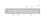
- FIG. 1 is a cross-sectional view schematically showing a configuration of an organic EL device according to a first embodiment. It is sectional drawing which shows typically the structure of the moisture absorption layer shown by FIG. It is sectional drawing which shows typically the structure of the moisture absorption layer in which a defect exists. It is a figure which shows the specification and lifetime test result of a moisture absorption layer which were used for experiment. It is a figure which shows the relationship between A / B and the estimated lifetime L.
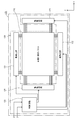
- FIG. It is a block diagram which shows typically schematic structure of the organic electroluminescence display which concerns on 2nd Embodiment.
- FIG. 7 is a plan view schematically showing an arrangement form of subpixels in the organic EL display panel shown in FIG. 6.
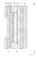
- FIG. 8 is a view of the AA cross section in FIG. 7 as seen from the direction of the arrow. It is sectional drawing of the 1 subpixel part of an organic electroluminescence display panel.
- An organic EL device includes an organic EL layer and a moisture absorption layer provided on at least one main surface side of the organic EL layer.
- the moisture absorption layer includes a moisture absorbent.
- B indicating the number of defects may be B ⁇ 1.
- first and second coating films may be inorganic films.
- the hygroscopic agent may be zeolite.
- the organic EL layer and at least one main surface of the organic EL layer are provided on both main surfaces of the first and second coated surfaces.
- the moisture absorption power (g / m 2 ) indicating the mass of moisture that can be absorbed per unit area of the moisture absorbing film is A
- the defect number b of the first and second coating films to be used is identified, the identified defect number b is defined as B, and the defect number b is used from the A obtained from the relationship between the A and the B.
- the hygroscopic power a of the hygroscopic film is set.
- a and B may be A / B ⁇ 0.2.
- the organic EL layer and at least one main surface side of the organic EL layer are provided, and both main surfaces of the moisture absorption film are the first and second coated surfaces.
- the hygroscopic film is manufactured so as to have a hygroscopic force equal to or higher than the hygroscopic force a set by the design method described above.
- FIG. 1 is a cross-sectional view schematically showing the configuration of the organic EL device according to the first embodiment.
- the organic EL device 1 includes a display unit 7 having an organic EL layer between an anode electrode and a cathode electrode.
- the organic EL device 1 has moisture absorption layers 5 and 9 on at least one main surface of the display unit 7, in this embodiment both main surfaces. That is, the display unit 7 is sandwiched between the moisture absorption layers 5 and 9.
- the organic EL device 1 includes a base 3, a moisture absorbing layer 5, a display unit 7, and a moisture absorbing layer 9 in this order.
- the organic EL device 1 has a surface coating layer 11 on the opposite side of the moisture absorption layer 9 from the display unit 7.
- the front side of the organic EL device 1 is the surface coating layer 11 side
- the back side is the base 3 side.
- Base The base 3 has a function of supporting the display unit 7 and the like. That is, the hygroscopic layer 5, the display unit 7, the hygroscopic layer 9, and the surface coating layer 11 are provided (stacked) on the upper surface of the base 3.
- the material of the base 3 resin material, ceramic material, metal material, etc. can be used.
- the organic EL device 1 according to the present embodiment has bendable flexibility. For this reason, a flexible resin material is preferably used as the base 3.
- the base 3 is preferably made of a material having a low moisture permeability (hereinafter referred to as “water vapor permeability”).
- a resin film made of a resin material is preferably used for the base 3.
- the moisture absorbing layers 5 and 9 have a waterproof function as a barrier against moisture intrusion from the front and back surfaces of the organic EL device 1 into the display unit 7. Details of the moisture absorbing layers 5 and 9 will be described later.
- (3) Display unit The light emission performance of the display unit 7 is degraded by moisture that has entered the organic EL layer or moisture absorbed by the organic EL layer.
- the surface coating layer 11 covers the display unit 7. Precisely, the surface covering layer 11 is formed in a layer shape on the upper surface of the moisture absorbing layer 9 and indirectly covers the display unit 7.
- the surface coating layer 11 has a protective function for preventing the display unit 7 from being directly damaged when a mechanical impact is applied to the organic EL device 1.
- the surface coating layer 11 has a function to prevent the entry of gas such as moisture and oxygen into the display unit 7 although it is not perfect.
- the material of the surface coating layer 11 for example, a resin film made of a resin material, a nitride film such as silicon nitride, an oxide film such as silicon oxide, a metal film, or the like is used.
- the organic EL device 1 has flexibility as described above. For this reason, a resin material having flexibility is used for the surface coating layer 11.
- the surface coating layer 11 is preferably made of a material having a low water vapor transmission rate in consideration of the influence of moisture on the organic EL layer, but a resin material is preferably used for the surface coating layer 11 in order to have flexibility. Is done. 2. About a moisture absorption layer Drawing 2 is a figure showing the section of a moisture absorption layer. (1) Whole The hygroscopic layers 5 and 9 may have the same configuration or different configurations. In the present embodiment, the configuration is the same. The moisture absorption layers 5 and 9 have the 1st coating film 21, the moisture absorption film
- the 1st coating film 21, the moisture absorption film 23, and the 2nd coating film 25 are laminated
- the first coating film 21 is disposed on the side close to the outside air (the side on which the base 3 and the surface coating layer 11 are present), and the second coating film 25 is disposed on the side close to the display unit 7. That is, in the moisture absorption layer 5, the first coating film 21 is arranged on the side close to the base 3, and in the moisture absorption layer 9, the first coating film 21 is arranged on the side close to the surface coating layer 11. Yes.
- the 1st coating film 21 suppresses the penetration
- the hygroscopic film 23 absorbs moisture that has been transmitted through the coating film 21 without being suppressed by the first coating film 21.
- the second coating film 25 suppresses the penetration of moisture that has permeated through the first coating film 21 and moisture absorbed by the moisture absorption film 23 into the display unit 7 side. With this configuration, the moisture absorption layers 5 and 9 prevent moisture from entering the display unit 7 from outside air.
- the first and second coating films 21 and 25 may have the same configuration or different configurations. In the present embodiment, the configuration is the same. For this reason, when it is not necessary to distinguish both irrespective of arrangement
- the first and second coating films 21 and 25 are made of a material having a low water vapor transmission rate. Specifically, a material lower than the water vapor transmission rate of the base 3 and the surface coating layer 11 is used as the material of the first and second coating films 21 and 25. More specifically, the water vapor transmission rate of the first and second covering layer 21, 25, 40 ° C., in an atmosphere of RH 90%, 1 ⁇ 10 -4 g / m 2 / day or more 1 ⁇ 10 - It is about 6 g / m 2 / day or less.
- the water vapor permeability of the first and second coating films 21 and 25 is preferably as small as possible.
- An example of a material having a low water vapor transmission rate is an inorganic film.
- examples of such an inorganic film include a nitride film such as silicon nitride, an oxide film such as silicon oxide, an oxynitride film such as silicon oxynitride, and a metal oxide film such as indium tin oxide (ITO) and silver oxide. It is done.
- Such an inorganic film is formed by, for example, a vacuum film forming method such as CVD or sputtering.
- the defect 31 here is a thing which permeate
- an inorganic film is formed by a vacuum film formation method, a locally generated pinhole or the like corresponds to the defect 31.
- Hygroscopic film The hygroscopic film 23 absorbs moisture that has entered the hygroscopic layers 5 and 9 mainly through the defects 31 of the first coating film 21. As a result, the moisture that has entered from the defects 31 of the first coating film 21 is suppressed from reaching the display unit 7.
- the moisture absorption film 23 is basically composed of a material that absorbs moisture.
- the hygroscopic film may be made of, for example, a resin material (highly hygroscopic), a porous material, or a fiber material.
- membrane 23 5 mass% or more is preferable.
- the hygroscopic film 23 may be made of a material containing a hygroscopic agent.
- the hygroscopic film 23 is configured by mixing a hygroscopic agent 27 with a base material 29.
- a chemical desiccant or a physical desiccant is used as the moisture absorbent 27 .
- the chemical desiccant uses the intrinsic properties (chemical reaction and deliquescence) of chemical substances, such as calcium oxide (CaO), calcium chloride (CaCl), barium oxide (BaO), sodium hydroxide (NaOH). Etc.
- the physical desiccant utilizes the property that water molecules are easily adsorbed on the porous surface, and examples thereof include silica gel, aluminum oxide, molecular sieve, allophane, and zeolite.
- a ceramic material As the base material 29, a ceramic material, an organic material, or the like is used.
- the ceramic material include YAG (yttrium aluminate) ceramic and alumina (aluminum oxide) ceramic.
- organic material examples include acrylic resin, polycarbonate resin, polyethylene terephthalate resin, polyvinyl chloride resin, polystyrene resin, epoxy resin, and silicone resin.
- the material of the base material 29 is appropriately selected depending on the intended use of the display unit 7. For example, when flexibility is required for the display unit 7 (and the moisture absorption layers 5 and 9), a resin material is preferably selected. When the moisture absorption layer 5 requires translucency, a material having translucency is selected. In the case of manufacturing at low cost, an organic material is selected. 3. Performance As a result of various studies, the inventors have used the first and second coating films 21 even when a material having a low water vapor transmission rate is used as the first and second coating films 21 and 25 of the moisture absorption layers 5 and 9. , 25, it is determined that moisture permeation through the first and second coating films 21, 25 cannot be completely suppressed.
- the inventors have further studied and have found that the influence on the display unit 7 can be estimated from the relationship between the hygroscopic force of the hygroscopic film 23 and the number of defects of the first and second coating films 21 and 25. .
- the inventors considered that the water vapor transmission rate of the coating film is greatly related to the defects of the coating film, but the relationship between the number of defects generated per unit area 1 m 2 and the hygroscopicity. could not be found.
- the local number (unit area 1 mm 2 ) is used to know the existence of a region where there are many defects, and by using the number of defects occurring in the local region, the number of defects and the display unit 7 can be determined for the first time. We were able to find a relationship between the impacts.
- the influence on the display unit 7 is specifically evaluated by the life of the display unit 7 (acceleration deterioration test). This can be said to be waterproof performance in actual use of the moisture absorption layers 5 and 9.
- Hygroscopic capacity is an inherent capacity of the material of the hygroscopic film 23, and the mass of moisture that can be absorbed by the hygroscopic film 23 of unit film thickness (unit: 1 ⁇ m) and unit area (unit: 1 m 2 ) (unit: g), and the unit is g / (m 2 ⁇ ⁇ m).
- the hygroscopic capacity is 1 [g / (m 2 ⁇ ⁇ m)].
- the “moisture absorption capacity” here is defined (adjusted) mainly by the content ratio of the moisture absorbent 27 to the base material 29.
- the moisture absorption capacity is obtained by multiplying the hygroscopic capacity by the film thickness of the hygroscopic film 23, that is, the mass (unit: g) of moisture that can be absorbed by the hygroscopic film 23 in a unit area (unit: 1 m 2 ). g / m 2 .
- the hygroscopic film 23 having a film thickness of 5 ⁇ m and a hygroscopic capacity of 1 [g / (m 2 ⁇ ⁇ m)] in the above example has a hygroscopic capacity of 5 [g / m 2 ].
- FIG. 3 is a schematic diagram showing a moisture absorption layer in which defects exist.
- the first and second coating films 21 and 25 have a defect 31 that occurs in the manufacturing process.
- the defect 31 referred to here is such that moisture passes through the first and second coating films 21 and 25 through the defect 31 as described above. That is, the defect 31 is a factor that causes water intrusion into the display unit 7.
- the foreign matter 33 and the dent 35, etc. present in the first and second coating films 21 and 25 are not the defects 31 here when moisture does not enter from the foreign matter 33 or the dent 35.
- the number of defects is defined by the number of defects 31 existing in a unit area (unit: 1 mm 2 ), and the unit is pieces / mm 2 .
- (3) Life (3-1) Experimental Results A life test was conducted on an organic EL device (display unit) having a moisture absorption layer. The life test is an acceleration deterioration test in a high temperature / high humidity atmosphere. Evaluation was made into the lifetime of the display part when the dark spot produced in the display part.
- Fig. 4 shows the specifications of the samples used in the life test and the results of the life test.
- Film thickness t is the film thickness of the hygroscopic film, and its unit is [ ⁇ m].
- adsorption capacity C indicates the mass of moisture absorbed by the hygroscopic film per unit area and unit film thickness, and the unit is [g / (m 2 ⁇ ⁇ m)].
- Adsorption power A indicates the mass of moisture that can be absorbed by the hygroscopic film per unit area, and its unit is [g / m 2 ]. This adsorption force A is equal to the product of the film thickness t and the moisture absorption capacity C.
- Defect number B indicates the number of defects per unit area of each of the first and second coating films, and the unit is [piece / mm 2 ].
- the first coating film corresponds to “barrier 1” in the drawing
- the second coating film corresponds to “barrier 2” in the drawing.
- “Lifetime experimental value l (lowercase L)” is the time until a dark spot occurs on the display unit, and its unit is [h].
- the “estimated life L” is calculated based on the result of the sample 1. This calculation utilizes the fact that “A / B” and the estimated life L are in a proportional relationship (see FIG. 5).
- a / B of barrier 1 is “0.13”, which is 0.667 times “0.20” which is the value of A / B of the barrier of sample 1.
- the estimated lifetime of barrier 1 of sample 2 is L (h) is 666.7 (h), which is obtained by multiplying the experimental lifetime value l of sample 1 by 0.667 which is the ratio of A / B of sample 1 and A / B of sample 2. .
- the barrier 1 and the barrier 2 in the A / B column are calculated corresponding to the barrier 1 and the barrier 2 in the defect number B column, respectively, and the average in the A / B column is A / B The average of barrier 1 and barrier 2 in the column.
- the barrier 1 and the barrier 2 in the column of the estimated life L are calculated corresponding to the barrier 1 and the barrier 2 in the column of A / B, respectively, and the average in the column of the estimated life L is the estimated life L It is the average of barrier 1 and barrier 2 in the column.
- the moisture absorption layer used for the sample uses silicon nitride for the first and second coating films 21 and 25.
- the hygroscopic film 23 uses zeolite as the hygroscopic agent 27 and acrylic resin as the base material 29.
- the acceleration deterioration test is performed on samples 1 to 5 having different moisture absorption film thicknesses t and defect counts B, respectively.
- sample 1 as a reference, regardless of the barriers 1 and 2, “A / B” is 0.2, and the lifetime experimental value l at this time is 1000 h.
- the estimated life L estimated from the results of A / B of sample 1 and the lifetime experimental value l and the lifetime experimental value l which is an actual experimental value are approximately. You can see that they match.
- FIG. 5 is a diagram showing the relationship between A / B and the estimated life L.
- A, B, and the like are the above-described hygroscopic force A and the number B of coating film defects.
- an estimated life L when A / B is a variable can be calculated by the following equation (1).
- the relationship between the hygroscopic force A and the number of defects B is obtained from the equation (2). It is done.
- the number of defects represented by “B” is a defect that occurs in the manufacturing process, and can be identified and identified in advance through experiments or the like. Specifically, when the number of defects in the coating film is specified as “b” by an experiment or the like, the moisture absorption power “a” of the moisture absorption film 23 when the number of defects in the coating film is “b” is (2) Obtained by the formula (3) based on the formula.
- A can be calculated from the hygroscopic capacity C and the film thickness t of the hygroscopic film by the following equation (4).
- the average value of A R / B R is “0.10”, and the lifetime experimental value l R at that time is “500”.
- the target life L in the acceleration deterioration test in the organic EL device in the present embodiment is 1000 (h) or more.
- This waterproof membrane is designed by the following procedures (i), (ii), and (iii).
- the adsorption force A R the number of defects B R in the moisture absorption layer, and the lifetime test value l R of the organic EL device are obtained, and the relationship between A and B is obtained from the target lifetime L of the device.
- This relational expression is obtained by, for example, the expression (2).
- the defect exists for each of the barrier 1 (first coating film) and the barrier 2 (second coating film).
- the defect number B as a reference may be the number of defects in the barrier 1, the number of defects in the barrier 2, or the average value of the barrier 1 and the barrier 2. Further, the larger of the number of defects of the barrier 1 and the barrier 2 may be used. Naturally, when the larger number of defects is adopted as a reference, the film thickness of the hygroscopic film 23 becomes larger and the lifetime becomes longer than when the smaller number of defects and the average value are adopted. Will be designed as follows.
- the number of defects as a reference may be the number of defects in the barrier 1 or the number of defects in the barrier 2 as described above. It may be an average value of the barrier 1 and the barrier 2. Further, the larger of the number of defects of the barrier 1 and the barrier 2 may be used.
- the number of defects indicates the number of defects of 1 mm 2
- the number of defects may be an average of a plurality of locations or a maximum value at a plurality of locations.
- the lifetime of the display unit is set to be longer than when the average is employed.
- the number of defects B is obtained by conducting an experiment or the like.
- “b” is specified in consideration of variations in the manufacturing process.
- “b” may be statistically specified from the number of defects in the prototype.
- the identified defect count b is “B”
- the hygroscopic force a of the hygroscopic film to be used is set from “A” obtained from the relationship between “A” and “B”.
- an organic EL device including a moisture absorbing layer that satisfies a target life can be manufactured.
- the manufacturing method of the organic EL device can be, for example, the following manufacturing method. That is, an organic EL device comprising: an organic EL layer; and a hygroscopic layer provided on at least one main surface of the organic EL layer and having both main surfaces of the hygroscopic film covered with the first and second coating films
- the hygroscopic film is manufactured so as to have a hygroscopic force equal to or higher than the hygroscopic force a set by the above-described design method.
- an organic EL display device will be described. 1. Schematic Configuration A schematic configuration of the organic EL display device 101 according to the second embodiment will be described with reference to FIGS. 6 and 7.
- FIG. 6 is a schematic block diagram showing a schematic configuration of the organic EL display device 101 according to the second embodiment.
- FIG. 7 is a schematic plan view showing an arrangement form of the subpixels 10a to 10c in the organic EL display panel 110.
- FIG. 6 is a schematic block diagram showing a schematic configuration of the organic EL display device 101 according to the second embodiment.
- FIG. 7 is a schematic plan view showing an arrangement form of the subpixels 10a to 10c in the organic EL display panel 110.
- the organic EL display device 101 includes an organic EL display panel 110 and a drive / control unit 120 connected thereto.
- the organic EL display panel 110 is an organic EL panel using an electroluminescence phenomenon of an organic material.
- the display surface of the organic EL display panel 110 is curved.
- a plurality of subpixels (subpixels) 10a to 10c are two-dimensionally arranged in the X-axis direction and the Y-axis direction.
- the subpixel 10a emits red light (R)
- the subpixel 10b emits green light (G)
- the subpixel 10c emits blue light (B).
- one pixel (pixel) as a display function is configured by a combination of three subpixels 10a to 10c adjacent in the X-axis direction.
- the organic EL display panel 110 has a cross-shaped bank (so-called “pixel bank”) 157, and the organic EL layer is formed in a region partitioned by the bank 157. ing.
- pixel bank cross-shaped bank
- FIG. 7 shows a region partitioned by the bank 157. For hatching.
- the drive / control unit 120 includes four drive circuits 121 to 124 and a control circuit 125.
- the arrangement relationship between the organic EL display panel 110 and the drive / control unit 120 in the organic EL display device 101 is not limited to the form shown in FIG.
- FIG. 8 is a view of the AA cross section in FIG. 7 as viewed from the direction of the arrow.
- the organic EL display panel 110 is disposed on the base 137 in a state where the display unit 131 is sandwiched between a pair of moisture absorption layers 133 and 135.
- the plurality of subpixels 10a to 10c are two-dimensionally provided in the display unit 131 in plan view.
- the subpixel region in which each of the subpixels 10a to 10c is formed has openings in a matrix shape in the X-axis direction and the Y-axis direction. It is an area partitioned into rectangular shapes.
- the display unit 131 has an insulating layer 153 stacked on a TFT substrate 151.
- the upper surface in the Z-axis direction of the insulating layer 153 is formed to be substantially flat.
- the TFT substrate 151 is simplified by omitting the illustration of the TFT layer and the like.
- An anode 155 is stacked in the subpixel region on the upper surface in the Z-axis direction of the insulating layer 153.
- banks 157 are formed so as to cover the insulating layer 153 and both edges of the anode 155 in the X-axis direction.
- An organic EL layer 159 is laminated on the upper surface of the anode 155 in the subpixel region partitioned by the bank 157.
- a cathode 161 is formed so as to cover the organic EL layer 159 and the upper part of the side surface and the top surface of the bank 157.
- a moisture absorption layer 135 is formed on the upper surface of the cathode 161.
- the moisture absorption layer 135 includes a second coating film 145, a moisture absorption film 143, and a first coating film 141.
- a surface coating layer 163 is formed on the upper surface of the moisture absorption layer 135.
- the surface coating layer 163 has a function of covering and protecting the display portion 131.
- the organic EL display panel 110 is a top emission type, and emits light upward in the Z-axis direction as indicated by an arrow in FIG. 3.
- Each constituent material (1) base of the organic EL display panel 110
- the base 137 needs to have a bendable flexibility.
- a resin material is preferably used as the base 137 as a flexible material.
- a polycarbonate film is used as the base 137.
- (2) Hygroscopic layer The hygroscopic layer 133 has the 1st coating film 141, the hygroscopic film 143, and the 2nd coating film 145 similarly to 1st Embodiment, and has the structure where these were laminated
- the first and second coating films 141 and 145 are made of a material having a low water vapor transmission rate.
- the water vapor transmission rate is 1 ⁇ 10 ⁇ 4 g / m 2 / day or more and 1 ⁇ 10 ⁇ 6 g / m 2 / day or less in an atmosphere of 40 ° C. and 90% RH, but a smaller one is preferable.
- the first and second coating films 141 and 145 have local defects that cannot be eliminated in manufacturing.
- an inorganic film made of an inorganic material is used.
- the inorganic film used for the first and second coating films 141 and 145 include thin films such as silicon nitride (SiN), silicon oxide (SiO 2), and silicon oxynitride (SiON), and indium tin oxide (ITO).
- a metal film or the like a silicon nitride (SiN) film is used for the first coating films 141 and 145.
- the moisture absorption film 143 absorbs moisture that has entered through the defects of the first and second coating films 141 and 145.
- the hygroscopic film 143 is formed by mixing a hygroscopic agent in a base material.
- aluminum oxide is used as the moisture absorbent
- acrylic resin which is an organic material, is used as the base material.
- (3) Display Unit (3-1) TFT Substrate The TFT substrate 151 includes a substrate and a TFT layer formed on the upper surface in the Z-axis direction of the substrate. Although not shown, the TFT layer is configured to include three electrodes of a gate, a source, and a drain, a semiconductor layer, a passivation film, and the like.
- the substrate serving as the base of the TFT substrate 151 is formed using a resin substrate or the like.
- a resin substrate either a thermoplastic resin or a thermosetting resin may be used.
- polyolefin such as polyethylene, polypropylene, ethylene-propylene copolymer, ethylene-vinyl acetate copolymer (EVA), cyclic polyolefin, modified polyolefin, polyvinyl chloride, polyvinylidene chloride, polystyrene, polyamide, polyimide (PI), Polyamideimide, polycarbonate, poly- (4-methylbenten-1), ionomer, acrylic resin, polymethyl methacrylate, acrylic-styrene copolymer (AS resin), butadiene-styrene copolymer, polio copolymer (EVOH) ), Polyesters such as polyethylene terephthalate (PET), polybutylene terephthalate, polyethylene naphthalate (PEN), precycl
- the insulating layer 153 is formed using an organic compound such as polyimide, polyamide, or acrylic resin material.
- the insulating layer 153 preferably has organic solvent resistance.
- the insulating layer 153 may be subjected to an etching process, a baking process, or the like during the manufacturing process, the insulating layer 153 is formed using a material having high resistance that does not excessively deform or deteriorate the process. It is desirable that (3-3) Anode
- the anode 155 is made of a metal material containing silver (Ag) or aluminum (Al). In the case of the organic EL display panel 110 according to this embodiment of the top emission type, it is preferable that the surface portion has high reflectivity.
- the anode 155 not only a single layer structure made of a metal material as described above, but also a laminate of a metal layer and a light-transmitting conductive layer can be adopted.
- a constituent material of the light transmissive conductive layer for example, indium tin oxide (ITO), indium zinc oxide (IZO), or the like can be used.
- Bank The bank 157 is formed using an organic material such as resin and has an insulating property. Examples of the organic material used for forming the bank 157 include acrylic resin, polyimide resin, and novolac type phenol resin.
- the organic EL layer 159 has a function of emitting light by generating an excited state when holes and electrons are injected and recombined.
- the material used for forming the organic EL layer 159 is a light-emitting organic material that can be formed by a wet printing method.
- the oxinoid compound, perylene compound, coumarin compound, azacoumarin compound, oxazole compound, oxadiazole compound, perinone compound, pyrrolopyrrole described in the patent publication (Japan / JP-A-5-163488) Compound, naphthalene compound, anthracene compound, fluorene compound, fluoranthene compound, tetracene compound, pyrene compound, coronene compound, quinolone compound and azaquinolone compound, pyrazoline derivative and pyrazolone derivative, rhodamine compound, chrysene compound, phenanthrene compound, cyclopentadiene compound, stilbene compound , Diphenylquinone compound, styryl compound, butadiene compound, dicyanomethylenepyran compound, dicyanomethylenethiopyran compound, fluorene
- the cathode 161 is formed using, for example, indium tin oxide (ITO) or indium zinc oxide (IZO).
- ITO indium tin oxide
- IZO indium zinc oxide
- Hygroscopic layer The hygroscopic layer 135 may be composed of the same material as the hygroscopic layer 133 or may be composed of another material.
- the moisture absorption layer 135 is made of the same material as the moisture absorption layer 133 described above.
- the moisture absorption layer 135 needs to be formed of a light transmissive material.
- the surface covering layer 163 covers the display unit 131.
- the surface coating layer 163 has a protective function for preventing the display portion 131 from being damaged by an impact or the like, and a function for suppressing the display portion 131 from being directly exposed to moisture or air.
- the surface coating layer 163 is formed using a material such as silicon nitride (SiN) or silicon oxynitride (SiON), for example.
- a material such as silicon nitride (SiN) or silicon oxynitride (SiON)
- a multilayer structure in which a resin material such as an acrylic resin or a silicone resin is further formed on a layer formed using a material such as silicon nitride (SiN) or silicon oxynitride (SiON) may be used.
- the surface covering layer 163 needs to be formed of a light-transmitting material.
- the moisture absorption layer is effective for a functional part that causes some performance degradation due to moisture absorption.
- a resin film having flexibility is used as the base 137, but a conventional glass material may be used as the base material.
- an organic EL device organic EL display device in which a glass material is used for the base and a moisture absorption layer is provided on the surface layer will be described.
- the organic EL display panel 201 has a structure in which a display unit 205 provided on a base 203 is covered with a moisture absorption layer 207. Note that the plurality of sub-pixels are provided in a two-dimensional plan view in the display unit 205, as in the second embodiment. Also in the third embodiment, as in the second embodiment, the sub-pixels for each color of R, G, and B have the same basic configuration. Therefore, in the following description, no distinction is made depending on the emission color. 2. Configuration (1) Base Unlike the base 137 of the second embodiment, the base 203 is made of a material that is not bendable, that is, has no flexibility at the implementation level. Here, the base 203 is made of a glass material.
- the glass material has a low water vapor transmission rate. For this reason, it is not necessary to provide a moisture absorption layer between the base 203 and the display unit 205. However, a moisture absorption layer may be provided between the base 203 and the display unit 205, and in that case, there is an advantage that the life of the display unit 205 can be extended or the thickness of the base 203 can be reduced.
- (2) Display Unit The display unit 205 is based on the TFT substrate 211, and an insulating layer 213 is stacked thereon. An anode 215 is formed in the subpixel region on the upper surface of the insulating layer 213. A bank 217 is formed so as to cover the insulating layer 213 and both edges of the anode 215 in the X-axis direction, and an organic EL layer 219 is formed in a region partitioned by the bank 217.
- a cathode 221 is formed so as to cover the organic EL layer 219 and the upper side surface and the top surface of the bank 217.
- (3) Hygroscopic layer The hygroscopic layer 207 has a structure having a first coating film 231, a hygroscopic film 233, and a second coating film 235, as in the second embodiment.
- the first and second coating films 231 and 235 are made of an inorganic material, and for example, a silicon nitride film is used.
- the hygroscopic film 233 uses zeolite particles as a hygroscopic agent, and uses polycarbonate as a resin material as a base material.
- the film thickness of the first coating film 231 in contact with the display unit 205 (or disposed on the side close to the display unit 205) is larger than the film thickness of the second coating film 235.
- the surface coating layer 209 is made of an inorganic material, for example, a silicon nitride film.
- the second coating film 235 of the hygroscopic layer may be made of an inorganic material, and in this case, the second coating film 235 may also serve as the surface coating layer.
- the moisture absorption layer is provided for the purpose of suppressing the ingress of moisture into the organic EL layer, but is not limited thereto.
- the moisture absorption layer can also be applied for the purpose of suppressing moisture intrusion into a functional layer other than the organic EL layer.
- the moisture absorption layer can suppress the ingress of moisture into the function layer, thereby suppressing the function deterioration of the function layer. it can.
- Hygroscopic layer (1) structure In the first, second, and third embodiments, only one hygroscopic layer is provided on one main surface of the display unit, but the present invention is not limited to this.
- a hygroscopic layer may be provided in multiple layers on one main surface such as a display unit. Thereby, a waterproof characteristic can be improved more.
- the hygroscopic layer 5 in the first embodiment includes the first coating film 21 on one main surface of the hygroscopic film 23 and the second coating film 25 on the other main surface.
- the hygroscopic layers 133 and 135 in the second embodiment include a first coating film 141 on one main surface of the hygroscopic film 143 and a second coating film 145 on the other main surface.
- the moisture absorption layer 207 in the third embodiment includes a first coating film 231 on one main surface of the moisture absorption film 233 and a second coating film 235 on the other main surface.
- the structure of the moisture absorption layer which concerns on 1 aspect of this invention is not restricted to these.
- each coating film may have the same configuration or a different configuration.
- the hygroscopic layer may include a plurality of hygroscopic films, for example, a laminated structure such as a coating film, a hygroscopic film, a coating film, a hygroscopic film, and a coating film.
- the plurality of hygroscopic films may have the same configuration or different configurations.
- the hygroscopic film 23 in the first embodiment, the hygroscopic film 143 in the second embodiment, and the hygroscopic film 233 in the third embodiment each contain one type of hygroscopic agent 27.
- the hygroscopic film may include a plurality of types of hygroscopic agents in one film.
- hygroscopic agent 27 in the first, second and third embodiments absorbs moisture (water vapor). However, it may absorb a gas (oxygen or the like) other than water vapor. Even in this case, it is possible to design a life in consideration of defects in the coating film by grasping the adsorption performance of the object to be absorbed by experiments or the like. 3.
- the organic EL device 1 according to the first embodiment, the organic EL display panel 110 of the organic EL display device 101 according to the second embodiment, and the organic EL display panel 201 according to the third embodiment are each provided with a display unit.
- a display unit For (7, 131, 205), one or two hygroscopic layers (5, 9, 133, 135, 207) are provided.
- a part of the structure of the display unit can also be used as a coating film on the side near the display unit in the moisture absorption layer.
- the display unit 131 of the second embodiment has a cathode 161.
- the cathode 161 is, for example, a metal oxide film of indium tin oxide (ITO) or indium zinc oxide (IZO) formed by sputtering
- the metal oxide film is used as a second coating near the functional portion in the moisture absorption layer. It can also be used as the covering film 145. 4).
- Display Unit The basic configuration of the display units 131 and 205 in the second and third embodiments has been described.
- the display unit includes a hole injection layer, a hole transport layer, an electron transport layer, an electron injection layer, and the like. You may prepare.
- the display units 131 and 205 in the second and third embodiments are the top emission type, but may be a bottom emission type.
- a light-transmitting material is used for the base, and a light-transmitting electrode is used as an electrode on the side close to the base (lower electrode; anodes 155 and 215 in the second and third embodiments). It is necessary to use a light-reflecting electrode as each (upper electrode; cathodes 161 and 221 in the second and third embodiments).
- the anodes 155 and 215 are arranged on the bases 137 and 203 side.
- a cathode may be arranged on the base side.
- the organic EL display device is described as a color organic EL display device.
- the present invention is not limited to this, and the configurations of the above-described embodiments and modifications can be applied to, for example, an organic EL display device for monochrome display.
- the configurations of the above embodiments and modifications can be applied to an organic EL light emitting device having a light control / color control function. That is, the organic EL device according to one embodiment of the present invention can be applied to an organic EL display device mainly having a function as a display, and can also be applied to an organic EL light emitting device mainly having a function as illumination. When applied as an organic EL light emitting device, the display unit does not have a display function, and thus becomes a light emitting unit.
- the present invention is useful for preventing moisture intrusion into the organic EL layer, whose function is reduced by moisture absorption.
Landscapes
- Physics & Mathematics (AREA)
- Optics & Photonics (AREA)
- Engineering & Computer Science (AREA)
- Manufacturing & Machinery (AREA)
- Electroluminescent Light Sources (AREA)
Abstract
Priority Applications (2)
| Application Number | Priority Date | Filing Date | Title |
|---|---|---|---|
| JP2016507130A JP6367920B2 (ja) | 2014-03-12 | 2014-07-09 | 有機el装置の設計方法及び有機el装置の製造方法 |
| US15/111,112 US9780334B2 (en) | 2014-03-12 | 2014-07-09 | Organic EL device having a hygroscopic layer |
Applications Claiming Priority (2)
| Application Number | Priority Date | Filing Date | Title |
|---|---|---|---|
| JP2014-049384 | 2014-03-12 | ||
| JP2014049384 | 2014-03-12 |
Publications (1)
| Publication Number | Publication Date |
|---|---|
| WO2015136580A1 true WO2015136580A1 (fr) | 2015-09-17 |
Family
ID=54071061
Family Applications (1)
| Application Number | Title | Priority Date | Filing Date |
|---|---|---|---|
| PCT/JP2014/003650 Ceased WO2015136580A1 (fr) | 2014-03-12 | 2014-07-09 | Dispositif électroluminescent organique, procédé de conception de dispositif électroluminescent organique et procédé de production de dispositif électroluminescent organique |
Country Status (3)
| Country | Link |
|---|---|
| US (1) | US9780334B2 (fr) |
| JP (1) | JP6367920B2 (fr) |
| WO (1) | WO2015136580A1 (fr) |
Cited By (1)
| Publication number | Priority date | Publication date | Assignee | Title |
|---|---|---|---|---|
| JP2017228510A (ja) * | 2016-06-24 | 2017-12-28 | 株式会社カネカ | 有機elパネル |
Families Citing this family (2)
| Publication number | Priority date | Publication date | Assignee | Title |
|---|---|---|---|---|
| CN112993190A (zh) * | 2021-02-07 | 2021-06-18 | 京东方科技集团股份有限公司 | 柔性显示基板及其制备方法和显示装置 |
| CN115084404A (zh) * | 2022-04-29 | 2022-09-20 | 固安翌光科技有限公司 | 一种封装结构 |
Citations (6)
| Publication number | Priority date | Publication date | Assignee | Title |
|---|---|---|---|---|
| JP2003007454A (ja) * | 2001-06-16 | 2003-01-10 | Cld Kk | 有機電界発光表示素子の製造方法、及び有機電界発光表示素子 |
| JP2005510757A (ja) * | 2001-11-29 | 2005-04-21 | デウ・エレクトロニクス・サービス・カンパニー・リミテッド | プラスチック基板の製造方法 |
| JP2006059620A (ja) * | 2004-08-19 | 2006-03-02 | Mitsui Chemicals Inc | 電子デバイス用封止フィルムおよびそれを用いた表示素子 |
| JP2006272190A (ja) * | 2005-03-29 | 2006-10-12 | Jsr Corp | 透明吸湿組成物、成形体、並びにフィルム及びその製造方法 |
| JP2013544012A (ja) * | 2010-10-25 | 2013-12-09 | ネダーランゼ・オルガニサティ・フォーア・トゥーゲパスト−ナトゥールヴェテンシャッペリーク・オンデルゾエク・ティーエヌオー | 光電子デバイス及び光電子デバイスの製造方法 |
| JP2014500582A (ja) * | 2010-10-25 | 2014-01-09 | ネダーランゼ・オルガニサティ・フォーア・トゥーゲパスト−ナトゥールヴェテンシャッペリーク・オンデルゾエク・ティーエヌオー | 有機光電子デバイス、及び、その製造方法 |
Family Cites Families (24)
| Publication number | Priority date | Publication date | Assignee | Title |
|---|---|---|---|---|
| JPH05163488A (ja) | 1991-12-17 | 1993-06-29 | Konica Corp | 有機薄膜エレクトロルミネッセンス素子 |
| US5443922A (en) | 1991-11-07 | 1995-08-22 | Konica Corporation | Organic thin film electroluminescence element |
| JP3170105B2 (ja) * | 1993-07-01 | 2001-05-28 | キヤノン株式会社 | 太陽電池モジュール |
| JP2001068266A (ja) | 1999-08-24 | 2001-03-16 | Toyota Motor Corp | 有機el素子及びその製造方法 |
| US6465953B1 (en) | 2000-06-12 | 2002-10-15 | General Electric Company | Plastic substrates with improved barrier properties for devices sensitive to water and/or oxygen, such as organic electroluminescent devices |
| US6924594B2 (en) * | 2000-10-03 | 2005-08-02 | Semiconductor Energy Laboratory Co., Ltd. | Light emitting device |
| JP4926324B2 (ja) * | 2001-02-08 | 2012-05-09 | 三星モバイルディスプレイ株式會社 | 有機elデバイス |
| KR20040027940A (ko) * | 2001-08-20 | 2004-04-01 | 노바-플라즈마 인크. | 기체 및 증기 침투율이 낮은 코팅층 |
| JP3810725B2 (ja) * | 2001-09-21 | 2006-08-16 | 株式会社半導体エネルギー研究所 | 発光装置及び電子機器 |
| JP4820536B2 (ja) * | 2003-06-25 | 2011-11-24 | 彬雄 谷口 | 有機エレクトロルミネッセンス素子の製造方法 |
| US20080032067A1 (en) * | 2006-07-24 | 2008-02-07 | Fujifilm Corporation | Cellulose acylate film, and polarizing plate and liquid crystal display device using the same |
| US20090001360A1 (en) | 2007-06-29 | 2009-01-01 | Masaya Nakayama | Organic el display and method for producing the same |
| JP5330739B2 (ja) | 2007-06-29 | 2013-10-30 | ユー・ディー・シー アイルランド リミテッド | 有機el表示装置およびその製造方法 |
| US8182102B2 (en) * | 2008-03-28 | 2012-05-22 | Fujifilm Corporation | Transparent support, optical film, polarizing plate and image display device |
| DE102009023350A1 (de) * | 2009-05-29 | 2010-12-02 | Osram Opto Semiconductors Gmbh | Elektronisches Bauelement und Verfahren zur Herstellung eines elektronischen Bauelements |
| EP2273579A1 (fr) | 2009-07-10 | 2011-01-12 | Nederlandse Organisatie voor toegepast -natuurwetenschappelijk onderzoek TNO | Procédé d'encapsulation de structure multicouche optoélectronique flexible |
| JP5616125B2 (ja) | 2010-05-24 | 2014-10-29 | 国立大学法人横浜国立大学 | 微細ゼオライトの製法 |
| WO2013021924A1 (fr) * | 2011-08-05 | 2013-02-14 | 三菱化学株式会社 | Dispositif émettant de la lumière électroluminescent organique et son procédé de fabrication |
| JP5805470B2 (ja) | 2011-08-31 | 2015-11-04 | 国立大学法人横浜国立大学 | 微細ゼオライトの製法 |
| US20130248827A1 (en) * | 2012-03-26 | 2013-09-26 | Canon Kabushiki Kaisha | Organic electroluminescence display device |
| CA2879447C (fr) * | 2012-07-19 | 2018-02-06 | Asahi Kasei Fibers Corporation | Structure multicouche comprenant une couche de cellulose a fibres minces |
| TWI572600B (zh) * | 2013-01-10 | 2017-03-01 | Konica Minolta Inc | 樹脂組成物、三唑化合物、光學薄膜、偏光板、光學透鏡、圓偏光板、及圖像顯示裝置 |
| KR20150119024A (ko) * | 2013-03-12 | 2015-10-23 | 코니카 미놀타 가부시키가이샤 | 유기 일렉트로루미네센스 표시 장치 및 그 제조 방법 |
| EP2924757A1 (fr) * | 2014-03-28 | 2015-09-30 | Nederlandse Organisatie voor toegepast- natuurwetenschappelijk onderzoek TNO | Stratifié de film barrière et dispositif électronique comprenant un tel stratifié |
-
2014
- 2014-07-09 WO PCT/JP2014/003650 patent/WO2015136580A1/fr not_active Ceased
- 2014-07-09 US US15/111,112 patent/US9780334B2/en not_active Expired - Fee Related
- 2014-07-09 JP JP2016507130A patent/JP6367920B2/ja not_active Expired - Fee Related
Patent Citations (6)
| Publication number | Priority date | Publication date | Assignee | Title |
|---|---|---|---|---|
| JP2003007454A (ja) * | 2001-06-16 | 2003-01-10 | Cld Kk | 有機電界発光表示素子の製造方法、及び有機電界発光表示素子 |
| JP2005510757A (ja) * | 2001-11-29 | 2005-04-21 | デウ・エレクトロニクス・サービス・カンパニー・リミテッド | プラスチック基板の製造方法 |
| JP2006059620A (ja) * | 2004-08-19 | 2006-03-02 | Mitsui Chemicals Inc | 電子デバイス用封止フィルムおよびそれを用いた表示素子 |
| JP2006272190A (ja) * | 2005-03-29 | 2006-10-12 | Jsr Corp | 透明吸湿組成物、成形体、並びにフィルム及びその製造方法 |
| JP2013544012A (ja) * | 2010-10-25 | 2013-12-09 | ネダーランゼ・オルガニサティ・フォーア・トゥーゲパスト−ナトゥールヴェテンシャッペリーク・オンデルゾエク・ティーエヌオー | 光電子デバイス及び光電子デバイスの製造方法 |
| JP2014500582A (ja) * | 2010-10-25 | 2014-01-09 | ネダーランゼ・オルガニサティ・フォーア・トゥーゲパスト−ナトゥールヴェテンシャッペリーク・オンデルゾエク・ティーエヌオー | 有機光電子デバイス、及び、その製造方法 |
Cited By (1)
| Publication number | Priority date | Publication date | Assignee | Title |
|---|---|---|---|---|
| JP2017228510A (ja) * | 2016-06-24 | 2017-12-28 | 株式会社カネカ | 有機elパネル |
Also Published As
| Publication number | Publication date |
|---|---|
| US9780334B2 (en) | 2017-10-03 |
| JP6367920B2 (ja) | 2018-08-01 |
| JPWO2015136580A1 (ja) | 2017-04-06 |
| US20160351853A1 (en) | 2016-12-01 |
Similar Documents
| Publication | Publication Date | Title |
|---|---|---|
| US8569951B2 (en) | Organic light-emitting display apparatus and method of manufacturing the same | |
| KR101420332B1 (ko) | 유기 발광 디스플레이 장치 | |
| CN104051493B (zh) | 有机发光显示装置 | |
| CN102450102B (zh) | 有机el显示装置及其制造方法 | |
| US10811631B2 (en) | Thin film transistor element substrate, method of producing the substrate, and organic EL display device including the thin film transistor element substrate | |
| KR101931174B1 (ko) | 유기 발광 표시 장치 및 그 제조방법 | |
| JP2000260572A (ja) | 有機エレクトロルミネッセンスパネル | |
| JP2014067598A (ja) | 有機エレクトロルミネッセンスパネル及びその製造方法 | |
| US10056574B2 (en) | Organic EL display device | |
| JP6336042B2 (ja) | 有機el素子および有機el素子の製造方法 | |
| JP2016091841A (ja) | 有機発光デバイスと有機表示装置 | |
| JP6367920B2 (ja) | 有機el装置の設計方法及び有機el装置の製造方法 | |
| JP6332769B2 (ja) | 有機発光デバイスと有機表示装置 | |
| JP2003217829A (ja) | 有機elディスプレイパネル | |
| KR20130007871A (ko) | 유기발광소자 | |
| JP6439188B2 (ja) | 有機el表示パネル及び有機el表示装置 | |
| JP6387562B2 (ja) | 有機発光デバイスおよび有機表示装置 | |
| US9799850B2 (en) | Organic EL device | |
| KR102673970B1 (ko) | 유기발광 표시장치 그 제조방법 | |
| JP6405587B2 (ja) | 有機elパネル及びその製造方法、並びにカラーフィルター基板 | |
| JP6098090B2 (ja) | 有機エレクトロルミネッセンスパネルの製造方法 | |
| JP2016004109A (ja) | 表示装置 | |
| WO2015145966A1 (fr) | Panneau d'affichage électroluminescent organique, procédé de fabrication de panneau d'affichage électroluminescent organique et procédé d'étanchéité d'élément électroluminescent organique | |
| JP2009009725A (ja) | 有機el表示装置 |
Legal Events
| Date | Code | Title | Description |
|---|---|---|---|
| 121 | Ep: the epo has been informed by wipo that ep was designated in this application |
Ref document number: 14885708 Country of ref document: EP Kind code of ref document: A1 |
|
| WWE | Wipo information: entry into national phase |
Ref document number: 15111112 Country of ref document: US |
|
| ENP | Entry into the national phase |
Ref document number: 2016507130 Country of ref document: JP Kind code of ref document: A |
|
| NENP | Non-entry into the national phase |
Ref country code: DE |
|
| 122 | Ep: pct application non-entry in european phase |
Ref document number: 14885708 Country of ref document: EP Kind code of ref document: A1 |