WO2015137018A1 - Dispositif mesure de tension sans contact - Google Patents
Dispositif mesure de tension sans contact Download PDFInfo
- Publication number
- WO2015137018A1 WO2015137018A1 PCT/JP2015/053149 JP2015053149W WO2015137018A1 WO 2015137018 A1 WO2015137018 A1 WO 2015137018A1 JP 2015053149 W JP2015053149 W JP 2015053149W WO 2015137018 A1 WO2015137018 A1 WO 2015137018A1
- Authority
- WO
- WIPO (PCT)
- Prior art keywords
- voltage
- unit
- voltage signal
- impedance
- electric field
- Prior art date
- Legal status (The legal status is an assumption and is not a legal conclusion. Google has not performed a legal analysis and makes no representation as to the accuracy of the status listed.)
- Ceased
Links
Images


Classifications
-
- G—PHYSICS
- G01—MEASURING; TESTING
- G01R—MEASURING ELECTRIC VARIABLES; MEASURING MAGNETIC VARIABLES
- G01R15/00—Details of measuring arrangements of the types provided for in groups G01R17/00 - G01R29/00, G01R33/00 - G01R33/26 or G01R35/00
- G01R15/14—Adaptations providing voltage or current isolation, e.g. for high-voltage or high-current networks
- G01R15/16—Adaptations providing voltage or current isolation, e.g. for high-voltage or high-current networks using capacitive devices
-
- G—PHYSICS
- G01—MEASURING; TESTING
- G01R—MEASURING ELECTRIC VARIABLES; MEASURING MAGNETIC VARIABLES
- G01R1/00—Details of instruments or arrangements of the types included in groups G01R5/00 - G01R13/00 and G01R31/00
- G01R1/02—General constructional details
- G01R1/06—Measuring leads; Measuring probes
- G01R1/067—Measuring probes
- G01R1/07—Non contact-making probes
-
- G—PHYSICS
- G01—MEASURING; TESTING
- G01R—MEASURING ELECTRIC VARIABLES; MEASURING MAGNETIC VARIABLES
- G01R1/00—Details of instruments or arrangements of the types included in groups G01R5/00 - G01R13/00 and G01R31/00
- G01R1/02—General constructional details
- G01R1/18—Screening arrangements against electric or magnetic fields, e.g. against earth's field
Definitions
- the present invention relates to a non-contact voltage measuring device that measures an alternating voltage flowing through a conductor without contacting the conductor.
- Non-contact voltage measuring device that measures an AC voltage (voltage to be measured) flowing through a conducting wire in an insulating-coated wiring without contacting the conducting wire. Examples of such a non-contact voltage measuring device are shown in Patent Documents 1 to 3.
- a non-contact voltage measuring device includes a probe and an electric circuit.
- a probe When a probe is brought close to a wiring so that a coupling capacitance is generated between the probe and the wiring, the electric circuit is passed through the probe.
- the voltage to be measured is derived based on the voltage signal input to.
- noise may be superimposed on the voltage signal in the electric circuit due to capacitive coupling between the electric circuit and a voltage source other than the wiring. Noise superimposed on the voltage signal causes the measurement accuracy of the voltage to be measured to be reduced.
- an electric field shield for blocking an external electric field around the electric circuit.
- the present invention has been made in view of the above, and an object of the present invention is to accurately measure a voltage to be measured by suppressing a leakage current from flowing through a parasitic capacitance generated between an electric field shield and an electric circuit.
- the object is to provide a non-contact voltage measuring device capable of measuring.
- the non-contact voltage measuring device brings the probe close to the conductor without contact so that a coupling capacitance is generated between the probe and the conductor.
- the electric circuit has a first impedance having a different impedance value.
- the first impedance part is disposed closer to the probe than the second impedance part, and at least one of the first impedance parts is included in the electric circuit.
- a first electric field shield that blocks an electric field incident on the first impedance part by covering the part, and the second impedance part
- a voltage signal applying unit that generates an equal voltage signal equal to the voltage signal in the first impedance unit from the voltage signal in the first impedance unit, and applies the generated equal voltage signal to the first electric field shield.
- the voltage signal in the first impedance part of the electric circuit is equal to the voltage signal (equal voltage signal) applied to the first electric field shield. That is, the amplitude and phase of the two voltage signals are both equal. Therefore, the first impedance part of the electric circuit and the first electric field shield are always at the same potential.
- the parasitic capacitance generated between the first impedance part and the first electric field shield is substantially ineffective, and a leakage current from the first impedance part to the first electric field shield (or vice versa) does not occur.
- the voltage to be measured applied to the conducting wire can be accurately measured based on the voltage signal input to the electric circuit via the probe.
- the voltage to be measured can be measured with high accuracy by suppressing the leakage current from flowing through the parasitic capacitance generated between the electric field shield and the electric circuit.
- Embodiment 1 Hereinafter, an embodiment of the present invention will be described in detail with reference to FIG.
- FIG. 1 is a schematic diagram showing the configuration of the voltage measuring apparatus 1.
- the voltage measuring device 1 measures a measurement target voltage VL , which is a voltage (voltage signal, voltage signal waveform) of alternating current (frequency: f) flowing through a conductor in the wiring w (primary side wiring) without contact with the conductor. can do.
- the voltage measuring apparatus 1 includes a detection probe 11, an electric field shield 12, a derivation unit 13 (voltage derivation unit), and an electric circuit EC.
- the detection probe 11 includes an electrode that can be attached so as to be in close contact with the outer peripheral surface of the insulating coating of the wiring w.
- the detection probe 11 may include an insulating member that covers the electrode.
- the coupling capacitance C L of the capacitance value corresponding to the measurement target voltage V L is generated.
- An induced voltage is induced on the electrode of the detection probe 11 by the alternating current flowing in the wiring w.
- the induced voltage generated at the electrode of the detection probe 11 is input to an electric circuit EC that is electrically connected to the detection probe 11.
- Electrical circuit EC as an input voltage V in, to obtain the induced on the electrodes of the detection probe 11 induced voltage. Further, the electric circuit EC outputs the voltage at the detection point set in the electric circuit EC to the deriving unit 13 as the output voltage V out (detection point voltage signal).
- the electric circuit EC includes a high impedance part HI (first impedance part) having a relatively high impedance value and a low impedance part LOW (second impedance part) having a relatively low impedance value. Details of the electric circuit EC will be described later.
- the electric field shield 12 blocks the electric field incident on the electric circuit EC, thereby preventing capacitive coupling between the electric circuit EC and a voltage source other than the wiring w.
- the electric field shield 12 may be made of metal (shield metal).
- the electric field shield 12 includes a first electric field shield part 12A (first electric field shield) that covers the high impedance part HI of the electric circuit EC, and a second electric field shield part 12B (second electric field shield) that covers the low impedance part LOW. including.
- the first electric field shield part 12A and the second electric field shield part 12B are insulated.
- the first electric field shield part 12A only needs to cover at least a part of the high impedance part HI. Moreover, the 2nd electric field shield part 12B should just coat
- a parasitic capacitance C ppL is generated between the first electric field shield part 12A and the high impedance part HI.
- a parasitic capacitance Cp is generated between the second electric field shield part 12B and the low impedance part LOW.
- the deriving unit 13 derives the measurement target voltage V L based on the output voltage V out output from the electric circuit EC. Specifically, the deriving unit 13 derives the measurement target voltage V L according to the following equation.
- V out1 and V out2 mean the output voltage V out when the electric circuit EC is in the first state and the second state (described later), respectively.
- ⁇ 2 ⁇ f (f is the frequency of alternating current flowing in the wiring w).
- the parasitic capacitance C p 0 generated between the second electric field shield part 12B and the low impedance part LOW is set. As described below, the parasitic capacitance C p is invalidated by the operational amplifier 15.
- the electric circuit EC includes capacitors C 1 and C 2 , a detection resistor R 1 , a changeover switch 14, an operational amplifier 15 (second voltage signal application unit), and a drive voltage application unit 16 (voltage signal application unit).
- the drive voltage application unit 16 may be formed integrally with other parts of the electric circuit EC, or may be arranged on a substrate different from the substrate on which the electric circuit EC is arranged. A specific circuit configuration for realizing the electric circuit EC will be described in Embodiments 3 to 5.
- capacitors C 1, C 2 both are connected to the input point p1 to the input voltage V in from the detecting probe 11 is input.
- the detection resistor R 1 is attached between the capacitors C 1 and C 2 and the reference potential point GND.
- the detection point p2 described above is located between the capacitors C 1 and C 2 and the detection resistor R 1 .
- the input voltage V in input from the detection probe 11 to the electric circuit EC is divided into capacitors C 1 and C 2 and a detection resistor R 1 .
- the output voltage V out is equal to the partial pressure of the input voltage V in applied to the detection resistor R 1.
- the capacitance values of the capacitors C 1 and C 2 and the resistance value of the detection resistor R 1 are determined so that the output voltage V out is sufficiently small.
- Changeover switch 14 an electric circuit EC, (i) the capacitor C 1 has a first state in series connected between the coupling capacitance C L and the detection resistor R 1, (ii) the capacitor C 1 and capacitor C 2 Is switched between the second state connected in series between the coupling capacitor C L and the detection resistor R 1 .
- the input voltage V in includes a detection resistor R 1, is divided between the capacitor C 1.
- the detection resistor R 1 is divided between the capacitors C 1 and capacitor C 2.
- the changeover switch 14 an electric circuit EC, (i) the capacitor C 1 is the coupling capacitance C L and the first state of being connected in series between the detection resistor R 1, it is (ii) a capacitor C 2, coupling capacitor C L and a second state connected in series between the detection resistor R 1, may be configured to switch between.
- This configuration for example, in an electric circuit EC, between the input point p1 and the capacitor C 1, and, between the input point p1 and the capacitor C 2, respectively, be provided with a switch which can be switched on and off Can be realized.
- a portion having the same potential as the input point p1 in the electric circuit EC is referred to as a high impedance portion HI.
- a portion having the same potential as the detection point p2 is referred to as a low impedance portion LOW.
- the operational amplifier 15 connects between the low impedance part LOW and the second electric field shield part 12B in the electric circuit EC.
- the operational amplifier 15 functions to make the second electric field shield part 12B and the low impedance part LOW have the same potential. This is a so-called driven shield circuit technique.
- the operational amplifier 15 causes the low impedance part LOW and the second electric field shield part 12B to have the same potential. Therefore, the low impedance section LOW, no current flows through the parasitic capacitance C p which is generated between the second field shield portion 12B. Therefore, it is possible to eliminate the possibility of parasitic capacitance C p affects the detected value of the output voltage V out.
- a voltage equal to the voltage (output voltage V out ) in the low impedance part LOW is generated from the voltage (input voltage V in ) in the high impedance part HI, and the generated voltage is the second electric field. You may apply to the shield part 12B.
- the voltage measuring device 1 does not have to include the operational amplifier 15.
- the drive voltage application unit 16 is connected to the low impedance unit LOW of the electric circuit EC.
- Driving voltage applying unit 16 obtains the output voltage V out from the low-impedance part LOW, on the basis of the output voltage V out acquired, it generates an equal driving voltage V ppL to the input voltage V in (equipotential signal).
- the drive voltage application unit 16 generates a voltage signal waveform equal to the voltage signal waveform in the high impedance unit HI from the voltage signal waveform in the low impedance unit LOW.
- the drive voltage application unit 16 applies the generated drive voltage V ppL to the first electric field shield unit 12A. Since equal to the driving voltage V ppL and the input voltage V in, and the high impedance section HI, the same potential to the first field shield portion 12A that driving voltage V ppL is applied. That is, the drive voltage V ppL cancels the potential difference between the high impedance part HI and the first electric field shield part 12A.
- the parasitic capacitance C ppL generated between the high impedance part HI and the first electric field shield part 12A. In other words, the parasitic capacitance C ppL is substantially invalid. Therefore, the possibility that the parasitic capacitance C ppL affects the detected value of the output voltage Vout can be eliminated.
- the drive voltage application unit 16 is electrically connected to the low impedance unit LOW, and acquires the output voltage Vout directly from the low impedance unit LOW.
- the drive voltage application unit 16 may indirectly acquire the output voltage V out from the derivation unit 13 to which the output voltage V out is input from the low impedance unit LOW.
- the drive voltage application unit 16 includes a filter unit 161, a phase shift unit 162 (phase adjustment unit), and an amplification unit 163 (amplitude adjustment unit).
- the filter unit 161 removes noise from the output voltage Vout .
- the filter unit 161 outputs the output voltage Vout from which noise has been removed to the phase shift unit 162.
- the noise removed by the filter unit 161 may be, for example, noise that enters the electric circuit EC from the ground wire (reference potential point GND) or noise that is caused by electromagnetic waves that enter the electric circuit EC from the outside.
- Phase shifter 162 the phase of the output voltage V out that is input from the filter unit 161, so that the input voltage V in phase equal, the adjusting (phase shifting) the phase of the output voltage V out.
- phase shift unit 162 by increasing or decreasing the phase of the output voltage Vout, the output stage (i.e., low impedance portions LOW) phase of the output voltage V out at the coupling capacitor C L - capacitor C 1, between C 2 (i.e., high impedance section HI) to match the phase of the input voltage V in at.
- the output stage i.e., low impedance portions LOW
- C L - capacitor C 1 between C 2 (i.e., high impedance section HI) to match the phase of the input voltage V in at.
- phase difference between the output voltage V out and the input voltage V in can be calculated theoretically or experimentally based on the configuration of the electric circuit EC.
- the phase shift unit 162 by delaying 90 ° the phase of the output voltage V out, to match the phase of the input voltage V in the output voltage V out.
- the phase shift unit 162 adjusts the phase of the output voltage Vout in consideration of this change.
- the phase shift unit 162 from a different detection probe and the detection probe 11 may obtain the phase information of the input voltage V in.
- phase shifter 162 the phase of the voltage induced in the different detection probes in proximity to the wire w, and acquires a phase of the input voltage V in.
- coupling capacitance generated between the different detection probes and the wiring w is preferably small compared to the coupling capacitor C L that occurs between the detection probe 11 wires w.
- the smaller the coupling capacitance the smaller the variation in the phase of the induced voltage. Therefore, the phase shift unit 162 can acquire an accurate phase with little variation from another detection probe.
- the phase shifter 162 the phase information of the input voltage V in may be acquired from wire w.
- the phase shifter 162 outputs the phase-shifted output voltage Vout to the amplifier 163.
- the output voltage V out is equal to the partial pressure of the input voltage V in applied to the detection resistor R 1. Then, the partial pressure of the output voltage V out applied to the detection resistor R 1 may be computed theoretically or empirically.
- Amplifying unit 163 based on the partial pressure of the output voltage V out applied to the detection resistor R 1, and amplitude of the output voltage V out, the input voltage V in such that the amplitude becomes equal, the output voltage V out Adjust the amplitude.
- the amplifying unit 163 adjusts the amplitude of the output voltage Vout in consideration of this attenuation.
- the amplifying unit 163 applies the output voltage Vout whose phase and amplitude are adjusted to the first electric field shield unit 12A as the driving voltage VppL .
- Phase and amplitude of the drive voltage V ppL is equal to the phase and amplitude of the input voltage V in.
- the changeover switch 14 when switching the state of the electrical circuit EC, by partial pressure ratio between the capacitor C 1, C 2 and the detection resistor R 1 is changed, also changes the amplitude of the output voltage V out. Therefore, the amplifying unit 163 changes the amplification degree of the output voltage Vout according to the changeover of the changeover switch 14.
- the detection probe 11 is in contact with or close to the coating of the wiring w (wiring coating).
- FIG. 2 is a schematic diagram showing the detection probe 11 and the first electric field shield part 12A included in the voltage measuring device 1, and passes through the wiring w, the detection probe 11, and the first electric field shield part 12A, and the wiring w It is sectional drawing in a cross section perpendicular
- FIG. 2 virtually shows a parasitic capacitance C ps between the wiring w and the surface of the wiring coating, and a surface resistance R cs generated on the surface of the wiring coating.
- the first electric field shield part 12A is adjacent to the side surface of the detection probe 11 in a non-contact manner.
- the first electric field shield 12A and the detection probe 11 are electrically insulated by air or a dielectric.
- the first electric field shielding unit 12A is also in contact with the wiring coating.
- FIG. 3 is a perspective view showing the configuration of the detection probe 11 and the first electric field shield part 12A attached to the wiring w.
- the first electric field shield portion 12 ⁇ / b> A surrounds the side surface of the detection probe 11.
- the side surface of the detection probe 11 is a surface adjacent to the surface (surface) of the detection probe 11 that contacts the wiring coating.
- the first electric field shield portion 12A may be adjacent to a part of the side surface of the detection probe 11 in a non-contact manner.
- a surface resistance R cs also exists between the first electric field shield part 12 ⁇ / b> A and the detection probe 11.
- the first electric field shield portion 12A and the detection probe 11 are always at the same potential. Therefore, the current flows from the wiring w to the first electric field shield part 12A, but does not flow from the first electric field shield part 12A to the detection probe 11.
- the amount of current flowing from the wiring w into the detection probe 11 through the parasitic capacitance Cps and the surface resistance Rcs can be suppressed.
- the parasitic capacitance C ps is substantially invalid. Therefore, the measurement target voltage VL can be measured with high accuracy.
- the detection probe 11 and the first electric field shield portion 12A do not need to be in contact with the wiring w. Either one of the detection probe 11 and the first electric field shield part 12A may be in contact with the wiring w. Further, the distance between the first electric field shield portion 12A and the wiring w may be equal to or less than the distance between the detection probe 11 and the wiring w.
- FIG. 4 and 5 show a configuration according to a modification of the present embodiment.
- the detection probe 11 is close to the wiring w in a non-contact manner, while the first electric field shield portion 12A is in contact with the wiring w.
- the first electric field shield part 12 ⁇ / b> A enters between the surface of the detection probe 11 and the wiring w.
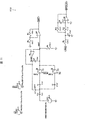
- FIG. 6 is a circuit diagram of the electric circuit EC1 according to the present embodiment.
- the electric circuit EC1 is an analog circuit, and includes a phase shift circuit and an amplifier circuit.
- the output stage “Out2” from the electric circuit EC1 and the input stage “Out3_AD” to the phase shift circuit are electrically connected.
- the phase shift circuit corresponds to the phase shift unit 162 of the first embodiment.
- Phase shift circuit by 90 ° phase shift the phase of the output voltage V out, the phase of the output voltage V out, to match the phase of the input voltage V in.
- the phase shift circuit shifts the phase of the output voltage Vout at another frequency (for example, 60 Hz) by 90 °, the constants (resistance value, capacitance value) of the circuit elements included in the phase shift circuit are reset. It is necessary to
- the amplification circuit corresponds to the amplification unit 163 of the first embodiment.
- the amplifier circuit includes switches S3 and S4.
- the switch S1, S2 (corresponding to the change-over switch 14 of the Embodiment 1) is switched, the amplifier circuit, by switching the switch S3, S4, and the amplitude of the output voltage V out, the amplitude of the input voltage V in Is changed so that the output voltage Vout is amplified.
- the electric circuit EC1 may further include a filter circuit for removing noise from the output voltage Vout .
- the filter circuit corresponds to the filter unit 161 in the first embodiment.
- the filter circuit is connected between the output stage “out2” from the electric circuit EC1 and the input stage “Out3_AD” to the phase shift circuit.
- the phase shift circuit corrects the phase adjustment amount of the output voltage Vout in consideration of the phase delay of the output voltage Vout in the filter circuit.
- the capacitance value of the parasitic capacitance C ppL was set to 3 pF, and the variation in the capacitance value of the parasitic capacitance C ppL was set to a uniform distribution of 10%. It is assumed that the variation in the output voltage Vout can be ignored because it is removed by calibration. Then, to calculate the error of the measurement target voltage V L when measured 100 times the target object voltage V L.
- the variation of the capacitance value of the parasitic capacitance C ppL was reset to 0% (no variation), and the error of the measurement target voltage V L was calculated without changing other conditions. .
- the error of the measurement target voltage VL measured by the voltage measurement apparatus 1 including the electric circuit ECX (see FIG. 11) according to the reference example was also calculated. Also in this calculation, the capacitance value of the parasitic capacitance C ppL was set to 3 pF. The variation of the capacitance value of the parasitic capacitance C ppL was set to 10% (uniform distribution from 0% to 10%). Further, it was assumed that the variation in the output voltage Vout can be ignored because it is removed by calibration.
- FIG. 10 is a schematic diagram showing a configuration of the voltage measuring device 9 including the electric circuit ECX according to the reference example.
- the voltage measuring device 9 according to the reference example does not include the drive voltage applying unit 16 and the point that the electric field shield 92 is not (electrically) divided into two parts as compared with the voltage measuring device 1. Is different.
- the electric field shield 92 corresponds to the second electric field shield part 12 ⁇ / b> B of the voltage measuring device 1.
- FIG. 11 is a circuit diagram of the electric circuit ECX (Driven Shield circuit) provided in the voltage measuring device 9 shown in FIG.
- the configuration of the electric circuit ECX shown in FIG. 11 is the same as the configuration of the electric circuit EC1 except that the phase shift circuit (phase shift unit 162) and the amplifier circuit (amplifier 163) are not provided.
- FIG. 7 shows the calculation result of the error of the measurement target voltage V L.
- the table in Figure 7 in addition to the calculated value of the error of the measurement target voltage V L, indicates the calculated value of the parasitic capacitance C ppL calculated based on the calculated value of the measurement target voltage V L.
- the left graph is a graph showing the time change of the leakage current I_C ppL flowing through the parasitic capacitance C ppL of the electric circuit EC1
- the right graph is the leakage flowing through the parasitic capacitance C ppL of the electric circuit ECX. It is a graph which shows the time change of electric current I_C ppL .
- the error (0.15%) of the measurement target voltage VL measured by the voltage measuring device 1 including the electric circuit EC1 is measured by the voltage measuring device 1 including the electric circuit ECX. Compared to the error (3.46%) of the measured voltage VL , it is 1/20 or less.
- the error of the measurement target voltage VL measured by the voltage measuring device 1 including the electric circuit EC1 is a variation in constants (resistance values, capacitance values) of circuit elements included in the drive voltage application unit 16 of the electric circuit EC1. Derived from. This error can be removed in the initial calibration.
- the error (0.15%) in the measurement target voltage VL is constant regardless of whether or not the parasitic capacitance C ppL varies. It is. Furthermore, according to the configuration according to the present embodiment, the calculated value of the parasitic capacitance C ppL is substantially zero (0.00 pF).
- the parasitic capacitance C ppL is substantially invalid.
- the error of the measurement target voltage VL is suppressed based on the configuration according to the present embodiment
- the measurement target voltage is similarly applied to the configurations according to other embodiments.
- the error of VL can be suppressed.
- phase shift unit 162 and the amplification unit 163 of the first embodiment are realized by a phase shift circuit and an amplification circuit, respectively.
- the phase shift unit 162 and the amplification unit 163 of the first embodiment are realized by a single integration circuit. Therefore, according to the configuration of the present embodiment, the electric circuit can be simplified as compared with the configuration shown in the third embodiment.
- FIG. 8 is a circuit diagram of the electric circuit EC2 according to the present embodiment. As shown in FIG. 8, the electric circuit EC2 is an analog circuit and includes an integration circuit.
- “Probe (Pr)” corresponds to the detection probe 11 (see FIG. 1).
- shield (Sh) corresponds to the first electric field shield portion 12A (see FIG. 1).
- the integration circuit corresponds to the phase shift unit 162 and the amplification unit 163 of the first embodiment. That is, the integrating circuit by the 90 ° phase the phase of the output voltage V out, the phase of the output voltage V out, to match the phase of the input voltage V in. Furthermore, the integration circuit, the amplitude of the output voltage V out, to match the amplitude of the input voltage V in.
- the integration circuit outputs the output voltage Vout having the adjusted phase shift and amplitude to the first electric field shield part 12A as the drive voltage VppL .
- a resistor may be connected in parallel with the capacitor C 3 and the capacitor C 4 shown in FIG.
- the configuration in which the drive voltage application unit 16 is realized by an analog circuit has been described.
- the drive voltage application unit 16 may be realized by a digital circuit.
- Digital circuits have the advantage that they are less susceptible to noise than analog circuits.
- phase shift unit 162 of the drive voltage application unit 16 is realized by a digital circuit.
- FIG. 9 is a schematic diagram of the drive voltage application unit 16 ′ according to the present embodiment.
- the drive voltage application unit 16 ′ includes a phase shift MPU 162 ′ and an amplification unit 163.
- the phase-shifting MPU 162 ′ includes an AD converter 1641, a phase increase / decrease unit 1642, and a DA converter 1643.
- the AD converter 1641 acquires the output voltage V out from the low impedance unit LOW, and AD converts the acquired output voltage V out . Then, the output voltage V out converted into a digital signal is output to the phase increase / decrease unit 1642.
- Phase adjuster 1642 and the phase of the output voltage V out that is input from the AD converter 1641, so that the input voltage V in phase equal increases or decreases the phase of the output voltage V out (adjustment). Thereafter, the phase increase / decrease unit 1642 outputs the output voltage V out to the DA converter 1643.
- the phase increase / decrease unit 1642 may adjust the phase of the output voltage V out by the same method as the phase shift unit 162 of the first embodiment.
- the DA converter 1643 converts the output voltage Vout input from the phase increase / decrease unit 1642 from a digital signal to an analog signal. Then, the output voltage V out converted into an analog signal is transmitted to the amplifying unit 163.
- the amplifying unit 163 applies the output voltage Vout whose phase and amplitude are adjusted to the first electric field shield unit 12A as the driving voltage VppL .
- an amplifier circuit that realizes the amplifying unit 163 may also be realized by a digital circuit.
- the control block (especially the phase shift unit 162 and the amplification unit 163) of the non-contact voltage measuring apparatus 1 may be realized by a logic circuit (hardware) formed in an integrated circuit (IC chip) or the like, or a CPU (Central Processing) Unit) and may be realized by software.
- a logic circuit hardware
- IC chip integrated circuit
- CPU Central Processing
- the non-contact voltage measuring apparatus 1 includes a CPU that executes instructions of a program that is software that implements each function, and a ROM (Read Only) in which the program and various data are recorded so as to be readable by a computer (or CPU).
- Memory or a storage device (these are referred to as “recording media”), a RAM (Random AccessMemory) for expanding the program, and the like.
- the objective of this invention is achieved when a computer (or CPU) reads the said program from the said recording medium and runs it.
- a “non-temporary tangible medium” such as a tape, a disk, a card, a semiconductor memory, a programmable logic circuit, or the like can be used.
- the program may be supplied to the computer via an arbitrary transmission medium (such as a communication network or a broadcast wave) that can transmit the program.
- a transmission medium such as a communication network or a broadcast wave
- the present invention can also be realized in the form of a data signal embedded in a carrier wave in which the program is embodied by electronic transmission.
- the non-contact voltage measuring device is configured such that when the probe is brought close to the conductor in a non-contact manner so that a coupling capacitance is generated between the probe and the conductor.
- the non-contact voltage measuring device for measuring a voltage to be measured applied to the conducting wire based on a voltage signal input to the electric circuit via the first impedance unit and the second impedance unit having different impedance values.
- the first impedance portion is disposed closer to the probe than the second impedance portion, and covers at least a part of the first impedance portion.
- a first electric field shield that blocks an electric field incident on the first impedance part, and a voltage signal in the second impedance part. Al, the equal and generates a voltage signal equal to the voltage signal at the first impedance unit, the generated above such a voltage signal, and a, and a voltage signal applying unit for applying to said first electric field shield.
- the voltage signal in the first impedance part of the electric circuit is equal to the voltage signal (equal voltage signal) applied to the first electric field shield. That is, the amplitude and phase of the two voltage signals are both equal. Therefore, the first impedance part of the electric circuit and the first electric field shield are always at the same potential.
- the parasitic capacitance generated between the first impedance part and the first electric field shield is substantially ineffective, and a leakage current from the first impedance part to the first electric field shield (or vice versa) does not occur.
- the voltage to be measured applied to the conducting wire can be accurately measured based on the voltage signal input to the electric circuit via the probe.
- the impedance value of the second impedance unit is lower than the impedance value of the first impedance unit.
- the non-contact voltage measurement device further includes a voltage deriving unit that derives the measurement target voltage based on a detection point voltage signal detected at a detection point set in the second impedance unit.
- the voltage signal applying unit may acquire the detection point voltage signal as a voltage signal in the second impedance unit.
- the equal voltage signal is generated from the detection point voltage signal detected at the detection point set in the second impedance portion of the electric circuit.
- the detection point voltage signal is a voltage signal that is measured in order to derive the voltage to be measured
- the electric circuit always has a configuration for outputting the detection point voltage signal. Therefore, it is not necessary to add a new circuit to the electric circuit in order to output the voltage signal in the second impedance unit.
- a non-contact voltage measuring device includes a second electric field shield that covers at least a part of the second impedance portion and is insulated from the first electric field shield, and the second electric field shield.
- a second voltage signal applying unit that applies an equal voltage signal equal to the voltage signal in the second impedance unit may be further provided.
- the second voltage signal application unit may include an operational amplifier, for example.
- the surface of the probe closest to the conducting wire is a surface
- the surface of the probe adjacent to the surface is a side surface.
- the first electric field shield may be adjacent to at least a part of the side surface without contact.
- At least a part of the side surface of the probe is adjacent to the first electric field shield. Therefore, when the voltage to be measured is measured, at least a part of the surface current flowing on the surface of the conductor coating flows into the first electric field shield instead of the probe.
- the amount of the surface current flowing into the probe can be suppressed as compared with the configuration in which the surface current flows only into the probe.
- the voltage signal applying unit (i) makes the amplitude of the voltage signal in the second impedance unit equal to the amplitude of the voltage signal in the first impedance unit. And (ii) a phase adjustment unit that adjusts the phase of the voltage signal in the second impedance unit to be equal to the phase of the voltage signal in the first impedance unit. Also good.
- the amplitude and phase of the voltage signal in the second impedance unit are adjusted so as to match the amplitude and phase of the voltage signal in the first impedance unit, respectively.
- an equal voltage signal equal to the voltage signal in the first impedance unit is generated from the voltage signal in the second impedance unit.
- the amplitude adjustment and phase adjustment of the voltage signal may be realized by a single member provided in the voltage signal application unit.
- the amplitude adjustment and phase adjustment of the voltage signal may be realized by an integration circuit.
- the non-contact voltage measuring device may be realized by a computer.
- the non-contact voltage measuring device is operated by operating the computer as each unit included in the non-contact voltage measuring device.
- a control program for a non-contact voltage measuring device that realizes the above on a computer and a computer-readable recording medium on which the control program is recorded also fall within the scope of the present invention.
- the present invention can be used in a voltage measuring device that measures an AC voltage flowing through a conductive wire in an insulating-coated wiring without contacting the conductive wire.
Landscapes
- Physics & Mathematics (AREA)
- General Physics & Mathematics (AREA)
- Measuring Instrument Details And Bridges, And Automatic Balancing Devices (AREA)
- Measurement Of Current Or Voltage (AREA)
- Measurement Of Resistance Or Impedance (AREA)
Abstract
La présente invention concerne un dispositif de mesure de tension sans contact (1) qui peut mesurer des tensions cibles avec une précision élevée en réduisant à un minimum les courants de fuite passant par l'intermédiaire d'une capacité parasite (CppL) entre des sections de protection contre les champs électriques (12) et un circuit électrique (EC). Une unité d'application de tension d'excitation (16) applique, à une première section de protection contre les champs électriques (12A) couvrant une section à haute impédance (HI) du circuit électrique (EC), une tension qui est générée à partir d'une tension de sortie (Vout) provenant d'une section à faible impédance (LOW) du circuit électrique (EC) et qui est égale à une tension d'entrée (Vin) à la section à haute impédance (HI).
Priority Applications (3)
| Application Number | Priority Date | Filing Date | Title |
|---|---|---|---|
| US15/119,400 US10215779B2 (en) | 2014-03-13 | 2015-02-04 | Non-contact voltage measurement device |
| EP15760679.9A EP3118635B1 (fr) | 2014-03-13 | 2015-02-04 | Dispositif mesure de tension sans contact |
| CN201580009037.3A CN106030320B (zh) | 2014-03-13 | 2015-02-04 | 非接触式电压测量装置 |
Applications Claiming Priority (2)
| Application Number | Priority Date | Filing Date | Title |
|---|---|---|---|
| JP2014050655A JP6343984B2 (ja) | 2014-03-13 | 2014-03-13 | 非接触電圧計測装置 |
| JP2014-050655 | 2014-03-13 |
Publications (1)
| Publication Number | Publication Date |
|---|---|
| WO2015137018A1 true WO2015137018A1 (fr) | 2015-09-17 |
Family
ID=54071470
Family Applications (1)
| Application Number | Title | Priority Date | Filing Date |
|---|---|---|---|
| PCT/JP2015/053149 Ceased WO2015137018A1 (fr) | 2014-03-13 | 2015-02-04 | Dispositif mesure de tension sans contact |
Country Status (5)
| Country | Link |
|---|---|
| US (1) | US10215779B2 (fr) |
| EP (1) | EP3118635B1 (fr) |
| JP (1) | JP6343984B2 (fr) |
| CN (1) | CN106030320B (fr) |
| WO (1) | WO2015137018A1 (fr) |
Cited By (2)
| Publication number | Priority date | Publication date | Assignee | Title |
|---|---|---|---|---|
| CN109387685A (zh) * | 2018-11-01 | 2019-02-26 | 华南理工大学 | 一种差分探头及非接触式电压测量装置 |
| TWI744409B (zh) * | 2016-11-11 | 2021-11-01 | 美商富克有限公司 | 使用參考信號的非接觸式電壓測量系統 |
Families Citing this family (13)
| Publication number | Priority date | Publication date | Assignee | Title |
|---|---|---|---|---|
| US10119998B2 (en) * | 2016-11-07 | 2018-11-06 | Fluke Corporation | Variable capacitance non-contact AC voltage measurement system |
| JP2018132346A (ja) * | 2017-02-14 | 2018-08-23 | 日置電機株式会社 | 電圧検出装置 |
| US10120021B1 (en) * | 2017-06-16 | 2018-11-06 | Fluke Corporation | Thermal non-contact voltage and non-contact current devices |
| JP6983093B2 (ja) * | 2018-03-27 | 2021-12-17 | 日東電工株式会社 | 抵抗測定装置、フィルム製造装置および導電性フィルムの製造方法 |
| JP7158938B2 (ja) * | 2018-07-26 | 2022-10-24 | 日置電機株式会社 | 信号生成装置および信号読取システム |
| CN110146733A (zh) * | 2019-05-10 | 2019-08-20 | 深圳市华星光电半导体显示技术有限公司 | 非接触电压测量装置及非接触电压测量方法 |
| CN113359059A (zh) * | 2020-03-02 | 2021-09-07 | 青岛经济技术开发区海尔热水器有限公司 | 漏电感应元件、漏电检测电路和热水器 |
| CN113341337A (zh) * | 2020-03-02 | 2021-09-03 | 青岛经济技术开发区海尔热水器有限公司 | 漏电感应元件、漏电检测电路和热水器 |
| CN111562427B (zh) * | 2020-05-25 | 2022-09-09 | 北京全路通信信号研究设计院集团有限公司 | 一种非接触式任意波形交变电压测量装置 |
| JP7608887B2 (ja) * | 2021-03-11 | 2025-01-07 | オムロン株式会社 | 非接触電圧測定装置 |
| EP4071488A1 (fr) * | 2021-04-08 | 2022-10-12 | ABB Schweiz AG | Interface de faible capacité pour la mesure du courant et de la tension à base de capteurs dans les réseaux haute tension ou les réseaux électriques |
| WO2023126991A1 (fr) * | 2021-12-27 | 2023-07-06 | 三菱電機株式会社 | Dispositif capteur de tension sans contact |
| CN115808578B (zh) * | 2022-12-02 | 2023-12-12 | 南方电网数字电网研究院有限公司 | 电力设备的电压获取方法、装置、设备、存储介质 |
Citations (2)
| Publication number | Priority date | Publication date | Assignee | Title |
|---|---|---|---|---|
| JPH0661654U (ja) * | 1993-02-09 | 1994-08-30 | 日産ディーゼル工業株式会社 | オイルタンクのキャップの構造 |
| JP2001324520A (ja) * | 2000-03-07 | 2001-11-22 | Sumitomo Metal Ind Ltd | インピーダンス検出回路、インピーダンス検出装置、及びインピーダンス検出方法 |
Family Cites Families (13)
| Publication number | Priority date | Publication date | Assignee | Title |
|---|---|---|---|---|
| US3444465A (en) * | 1966-07-05 | 1969-05-13 | Sylvania Electric Prod | Probe for a graphic communication system including means for eliminating shunt capacitance effects |
| US3798541A (en) * | 1970-10-30 | 1974-03-19 | Wilcom Prod Inc | Capacitive probe structure for testing the integrity of electrical cables and conductors |
| JPS58174856A (ja) | 1982-04-08 | 1983-10-13 | Yokogawa Hokushin Electric Corp | 非接触電圧計用結合電極 |
| FR2651889B1 (fr) | 1989-09-08 | 1991-11-29 | Alsthom Gec | Reducteur capacitif de tension electronique. |
| JP2581605Y2 (ja) * | 1992-09-01 | 1998-09-24 | 株式会社アドバンテスト | 非接触交流電圧計 |
| US5473244A (en) * | 1992-09-17 | 1995-12-05 | Libove; Joel M. | Apparatus for measuring voltages and currents using non-contacting sensors |
| TW546480B (en) * | 2000-03-07 | 2003-08-11 | Sumitomo Metal Ind | Circuit, apparatus and method for inspecting impedance |
| JP3761470B2 (ja) * | 2001-04-04 | 2006-03-29 | 北斗電子工業株式会社 | 非接触電圧計測方法及び装置並びに検出プローブ |
| JP2003028900A (ja) | 2001-07-11 | 2003-01-29 | Yokogawa Electric Corp | 非接触電圧測定方法およびその装置 |
| GB0129390D0 (en) | 2001-12-07 | 2002-01-30 | Clark Terrence D | Electrodynamic sensors and applications thereof |
| GB0614261D0 (en) | 2006-07-18 | 2006-08-30 | Univ Sussex The | Electric Potential Sensor |
| CN101881791B (zh) * | 2009-04-30 | 2015-08-05 | 日置电机株式会社 | 电压检测装置 |
| JP2012163394A (ja) | 2011-02-04 | 2012-08-30 | Hitachi Electric Systems Ltd | 非接触電圧検出装置 |
-
2014
- 2014-03-13 JP JP2014050655A patent/JP6343984B2/ja not_active Expired - Fee Related
-
2015
- 2015-02-04 CN CN201580009037.3A patent/CN106030320B/zh active Active
- 2015-02-04 WO PCT/JP2015/053149 patent/WO2015137018A1/fr not_active Ceased
- 2015-02-04 US US15/119,400 patent/US10215779B2/en active Active
- 2015-02-04 EP EP15760679.9A patent/EP3118635B1/fr active Active
Patent Citations (2)
| Publication number | Priority date | Publication date | Assignee | Title |
|---|---|---|---|---|
| JPH0661654U (ja) * | 1993-02-09 | 1994-08-30 | 日産ディーゼル工業株式会社 | オイルタンクのキャップの構造 |
| JP2001324520A (ja) * | 2000-03-07 | 2001-11-22 | Sumitomo Metal Ind Ltd | インピーダンス検出回路、インピーダンス検出装置、及びインピーダンス検出方法 |
Cited By (3)
| Publication number | Priority date | Publication date | Assignee | Title |
|---|---|---|---|---|
| TWI744409B (zh) * | 2016-11-11 | 2021-11-01 | 美商富克有限公司 | 使用參考信號的非接觸式電壓測量系統 |
| CN109387685A (zh) * | 2018-11-01 | 2019-02-26 | 华南理工大学 | 一种差分探头及非接触式电压测量装置 |
| CN109387685B (zh) * | 2018-11-01 | 2024-04-30 | 华南理工大学 | 一种差分探头及非接触式电压测量装置 |
Also Published As
| Publication number | Publication date |
|---|---|
| US20170059619A1 (en) | 2017-03-02 |
| EP3118635A1 (fr) | 2017-01-18 |
| JP2015175655A (ja) | 2015-10-05 |
| EP3118635B1 (fr) | 2020-04-15 |
| CN106030320A (zh) | 2016-10-12 |
| CN106030320B (zh) | 2019-08-06 |
| JP6343984B2 (ja) | 2018-06-20 |
| EP3118635A4 (fr) | 2018-01-24 |
| US10215779B2 (en) | 2019-02-26 |
Similar Documents
| Publication | Publication Date | Title |
|---|---|---|
| JP6343984B2 (ja) | 非接触電圧計測装置 | |
| US10228395B2 (en) | Non-contact voltage measurement device | |
| US8525529B2 (en) | Impedance detection circuit and adjustment method of impedance detection circuit | |
| WO2015083618A1 (fr) | Dispositif de mesure de tension sans contact et procédé associé | |
| CN110088637A (zh) | 静电电容检测装置以及输入装置 | |
| CN103339860B (zh) | 电容性近接传感器以及用于电容性近接检测的方法 | |
| JP6851785B2 (ja) | 電磁流量計 | |
| TWI687860B (zh) | 電容式感測系統中目標物件耦合至饋入線路之補償 | |
| US20080093925A1 (en) | Passenger detection apparatus for detecting breakage on shield line without being affected by peripheral shield cables | |
| JP4356570B2 (ja) | 静電容量型距離センサ | |
| WO2015137017A1 (fr) | Dispositif de mesure de tension sans contact | |
| JP5502597B2 (ja) | インピーダンス検出回路およびインピーダンス検出方法 | |
| JP7354432B2 (ja) | 静電容量検出装置及び入力装置 | |
| WO2014155680A1 (fr) | Dispositif de mesure de tension | |
| JP3501401B2 (ja) | インピーダンス検出回路、インピーダンス検出装置、及びインピーダンス検出方法 | |
| JP3501403B2 (ja) | インピーダンス検出回路、インピーダンス検出装置、及びインピーダンス検出方法 | |
| US12174047B2 (en) | Capacitance detection device and capacitance detection method | |
| JP6128921B2 (ja) | 非停電絶縁診断装置及び非停電絶縁診断方法 | |
| JP2016099207A (ja) | 電圧測定装置 | |
| WO2015133212A1 (fr) | Appareil de mesure de tension et procédé de mesure de tension | |
| TW202241050A (zh) | 放大電路及測量裝置 | |
| JP6625422B2 (ja) | 測定装置 | |
| JP6273443B2 (ja) | 物理量計測回路を用いた物理量計測方法 | |
| CN114553211A (zh) | 输入电路以及测定装置 |
Legal Events
| Date | Code | Title | Description |
|---|---|---|---|
| 121 | Ep: the epo has been informed by wipo that ep was designated in this application |
Ref document number: 15760679 Country of ref document: EP Kind code of ref document: A1 |
|
| REEP | Request for entry into the european phase |
Ref document number: 2015760679 Country of ref document: EP |
|
| WWE | Wipo information: entry into national phase |
Ref document number: 15119400 Country of ref document: US Ref document number: 2015760679 Country of ref document: EP |
|
| NENP | Non-entry into the national phase |
Ref country code: DE |