WO2015146257A1 - Mécanisme de rayonnement thermique pour appareil électronique et dispositif d'alimentation - Google Patents
Mécanisme de rayonnement thermique pour appareil électronique et dispositif d'alimentation Download PDFInfo
- Publication number
- WO2015146257A1 WO2015146257A1 PCT/JP2015/051713 JP2015051713W WO2015146257A1 WO 2015146257 A1 WO2015146257 A1 WO 2015146257A1 JP 2015051713 W JP2015051713 W JP 2015051713W WO 2015146257 A1 WO2015146257 A1 WO 2015146257A1
- Authority
- WO
- WIPO (PCT)
- Prior art keywords
- electronic component
- component mounting
- sheet
- filler
- heat dissipation
- Prior art date
- Legal status (The legal status is an assumption and is not a legal conclusion. Google has not performed a legal analysis and makes no representation as to the accuracy of the status listed.)
- Ceased
Links
Images


Classifications
-
- H—ELECTRICITY
- H05—ELECTRIC TECHNIQUES NOT OTHERWISE PROVIDED FOR
- H05K—PRINTED CIRCUITS; CASINGS OR CONSTRUCTIONAL DETAILS OF ELECTRIC APPARATUS; MANUFACTURE OF ASSEMBLAGES OF ELECTRICAL COMPONENTS
- H05K7/00—Constructional details common to different types of electric apparatus
- H05K7/20—Modifications to facilitate cooling, ventilating, or heating
- H05K7/2089—Modifications to facilitate cooling, ventilating, or heating for power electronics, e.g. for inverters for controlling motor
- H05K7/209—Heat transfer by conduction from internal heat source to heat radiating structure
Definitions
- the present invention relates to a heat dissipation mechanism and a power supply device for an electronic device including an electronic component mounting board on which an electronic component is mounted on a board, and a housing for housing the electronic component mounting board.
- a power supply device such as an AC adapter generally serves to convert a predetermined alternating voltage into a desired direct current (DC) voltage.
- DC direct current
- the effective value (RMS: Root Mean Square) of the AC voltage is 100V.
- a desired DC voltage supplied to a notebook personal computer (PC) is 19V.
- the above AC adapter is used as an external power source in a notebook computer or the like.
- a notebook computer or the like In recent years, with the spread of mobile personal computers and tablet personal computers, there is an increasing need for miniaturization of AC adapters that do not get in the way even when they are placed in a bag.
- the AC adapter includes a bipolar transistor and a MOS-FET (Metal Oxide Semiconductor Semiconductor Field Effect Transistor) and performs a switching operation.
- the AC adapter includes a diode and performs a rectifying operation determined by the potentials of both the anode and cathode terminals.
- the AC adapter includes a bridge diode for full-wave rectification of the AC voltage.
- cooling means in a conventional electronic device for example, an example of cooling a component on a solder surface of an electronic component shown in FIGS. 7A and 7B is known.
- an AC adapter 100 as an example of a conventional electronic device is an electronic component in which various electronic components 112 are fixed to a substrate 111 by soldering, as shown in FIGS.
- a mounting substrate 110 is provided.
- a lead-type foot-shaped component for example, an axial resistor, a large electrolytic capacitor, a transformer, a common choke coil, or a semiconductor TO-220 package
- surface mount type components are mounted on the back surface and soldered on the back surface.
- each protrusion 113 is the height of the surface mount component included in the protrusion 113 mounted on the back surface of the substrate 111. It depends on the type.
- the heat dissipating sheets 121 to 124 are cut out and used in layers.
- the substrate 111 is cooled by effectively transferring the heat from the heat-generating component such as a semiconductor to the aluminum plate 140 and the casing 150 without transferring the heat to the substrate 111.
- the heat-generating component such as a semiconductor
- this method has a problem in that it does not enter a necessary gap or spreads to an unnecessary part depending on the amount of insertion in advance and the pressure for assembling the substrate. Further, when the specific gravity of the elastic or plastic filler is heavy, there is a problem that the weight of the assembled electronic device varies due to the variation in the amount of insertion.
- the present invention has been made in view of the above-described conventional problems, and an object of the present invention is to provide a space between the back surface of the electronic component mounting board on which the protruding portions including a plurality of soldering portions are formed and the back surface side heat radiating metal plate. It is an object of the present invention to provide a heat dissipation mechanism and a power supply device for an electronic device that can efficiently fill the gap portion with a filler.
- an electronic device heat dissipation mechanism includes an electronic component mounting board on which an electronic component is mounted on a substrate, and a housing that houses the electronic component mounting board.
- a backside heat radiating metal plate covering at least the back surface of the electronic component mounting board, a back surface of the electronic component mounting board on which a protrusion including a plurality of soldering portions is formed, and the backside heat radiating metal plate, And a filler molded with a hole matched to the shape of the protrusion so as to be inserted into the gap between the two.
- a power supply device includes the above-described electronic device heat dissipation mechanism in order to solve the above-described problem.
- an electron that can efficiently fill the gap between the back surface of the electronic component mounting board on which the protruding portion including a plurality of soldering portions is formed and the heat radiation metal plate on the back surface can be filled with the filler.
- the effect is to provide a heat dissipation mechanism and a power supply device for the device.
- FIG. 2 is an exploded perspective view of the electronic device as viewed from above. It is a perspective view which shows the structure of the said electronic device.
- (A) is a rear view which shows the structure of the electronic component mounting board in the said electronic device
- (b) is a top view which shows the structure of the said electronic component mounting board
- (c) is the structure of the said electronic component mounting board
- (D) is a front view showing a configuration of the electronic component mounting substrate
- (e) is a right side view showing a configuration of the electronic component mounting substrate
- (f) is a side view showing the configuration of the electronic component mounting substrate. It is a bottom view which shows the structure of an electronic component mounting board.
- FIG. 2 is an exploded perspective view of the electronic device as viewed from above.
- (A)-(e) is a top view which shows the structure of the 1st sheet
- (A) shows the structure of the heat dissipation mechanism of the conventional electronic device, and is the exploded perspective view which looked at the electronic device from the lower side,
- (b) shows the structure of the heat dissipation mechanism of the said electronic device. It is the disassembled perspective view which looked at the electronic device from the upper side.
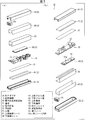
- FIG. 1A is an exploded perspective view showing the configuration of the heat dissipation mechanism 2 of the AC adapter 1A as the electronic apparatus according to the first embodiment, as viewed from the lower side of the AC adapter 1A.
- FIG. 1B shows the configuration of the heat dissipation mechanism 2 of the AC adapter 1A, and is an exploded perspective view of the AC adapter 1A as viewed from above.
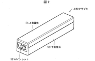
- FIG. 2 is a perspective view showing the configuration of the AC adapter 1A of the present embodiment.
- An AC (alternating current) alternating current (AC) adapter which is a power supply device as an electronic apparatus of the present embodiment, supplies power to, for example, a portable terminal that operates with a direct current (DC) power source. This is for converting the voltage into a DC voltage. For this reason, as shown in FIG. 2, an AC inlet 53 for connecting a cable (not shown) from an AC power source (not shown) is provided at one end of the AC adapter 1A. On the other hand, a DC cable for connecting to the portable terminal (not shown) is connected to the other end facing the one end of the AC adapter 1A.
- the AC adapter 1A of the present embodiment has, for example, an output of 65W (19V, 3.42A), a width of 26 mm, a length of 131 mm, a height of 25 mm, and a volume of about 85 cc. It has a shape.
- the general size of a conventional 65 W output AC adapter is, for example, 46 mm wide, 107.5 mm long, 29.6 mm high, and has a volume of about 150 cc.
- the AC adapter 1A of the present embodiment has a volume reduction of about 40% with the same output capacity as compared with the conventional product. Further, if the volume is reduced, the upper casing 51 and the lower casing 52 which are casings are also reduced, and the weight can be reduced. For this reason, even if it puts in a bag, it has the merit that it is not bulky.
- an AC (alternating current) adapter 1A that is a power supply device as an electronic device is illustrated, but in the present invention, the electronic device and the power supply device are not necessarily limited to the AC adapter 1A.
- another device such as a built-in power source for a desktop PC or a built-in power source for a TV may be used.
- FIG. 2 shows an example in which the stick shape is 85 cc and the aspect ratio between the width and the length is 5 or more.
- the shape has a width of 35 mm, a length of 96 mm, and a height of 25 mm.
- the aspect ratio between the width and the length may be 3 or less.
- the AC adapter 1 ⁇ / b> A covers an electronic component mounting substrate 10 in which a plurality of electronic components 12 are mounted on a substrate 11 by soldering, and covers the electronic component mounting substrate 10.
- An upper housing 51 and a lower housing 52 are provided as housings.
- an upper insulating sheet 31 that covers the electronic component mounting substrate 10 from the upper side an upper aluminum plate 41 that covers the upper insulating sheet 31 from the upper side, and an upper aluminum plate 41 that is on the upper side
- the upper casing 51 that covers from above.
- a molding filler 20 on the lower side of the electronic component mounting substrate 10, a molding filler 20, a lower insulating sheet 32 that covers the molding filler 20 from the lower side, and a rear surface side heat dissipation metal that covers the lower insulating sheet 32 from the lower side.
- a lower aluminum plate 42 as a plate and a lower housing 52 that covers the lower aluminum plate 42 from below are provided.
- the AC inlet 53 mentioned above is provided in the edge part of AC adapter 1A.
- the upper insulating sheet 31 and the lower insulating sheet 32 are a pair of two, for example, polycarbonate resin or hard paper.
- the lower insulating sheet 32 has a C channel cross section and covers the periphery of the electronic component mounting board 10.
- the upper insulating sheet 31 is a flat sheet and covers the upper surface of the lower insulating sheet 32.
- the shapes of the upper insulating sheet 31 and the lower insulating sheet 32 are not necessarily limited thereto, and the upper insulating sheet 31 may have a C-channel cross section, while the lower insulating sheet 32 may be a flat sheet.
- An upper aluminum plate 41 and a lower aluminum plate 42 are provided on the outer portions of the upper insulating sheet 31 and the lower insulating sheet 32.
- the upper aluminum plate 41 and the lower aluminum plate 42 are a pair of two, and are made of an aluminum material as a metal material having good thermal conductivity. Accordingly, the heat generated from the electronic component 12 of the electronic component mounting substrate 10 serves as a heat radiating fin by using the upper aluminum plate 41 and the lower aluminum plate 42 which are materials having good conductivity. ing.
- an aluminum material is used as a metal material.
- the present invention is not limited to this, and a material such as a copper plate as a metal material having good thermal conductivity can also be used.
- the upper housing 51 and the lower housing 52 form a pair of two, and each is formed in a box shape with resin. Therefore, when the upper housing 51 and the lower housing 52 are integrally combined, the electronic component mounting substrate 10 is completely accommodated.
- FIG. 3A is a rear view showing the configuration of the electronic component mounting board 10 in the AC adapter 1A.
- FIG. 3B is a plan view showing the configuration of the electronic component mounting board 10.
- FIG. 3C is a left side view showing the configuration of the electronic component mounting board 10.
- FIG. 3D is a front view showing the configuration of the electronic component mounting board 10.
- FIG. 3E is a right side view showing the configuration of the electronic component mounting board 10.
- FIG. 3F is a bottom view showing the configuration of the electronic component mounting board 10.
- the electronic component mounting substrate 10 includes a substrate 11 and a plurality of electronic components 12 mounted on the surface of the substrate 11 by soldering.
- the electronic component 12 mounted on the surface of the substrate 11 is composed of, for example, a transformer, an axial resistor, an electrolytic capacitor, and the like.
- the electronic component 12 is not necessarily limited to this, and may be another component.
- soldering portion for connecting the lead of the electronic component 12 mounted on the front surface of the substrate 11 on the back surface of the substrate 11 is formed on the back surface of the substrate 11, and an FET (Field effect transistor: Surface mount components such as field effect transistors or bridge diodes are provided.
- FET Field effect transistor: Surface mount components such as field effect transistors or bridge diodes are provided.
- the soldering portion and the surface mounting component are the protruding portions 13 protruding from the substrate 11. Accordingly, the plurality of protrusions 13 have different shapes and sizes depending on each surface-mounted component mounted on the back surface of the substrate 11.
- the FET is a lead package such as a three-terminal regulator TO (TransistorlineOutline) 220 package, and includes a heat radiation fin made of aluminum (Al) or copper (Cu).
- the electronic component mounting substrate 10 in the AC adapter 1A of the present embodiment is a small one, and the FET is made of a TO252 package. Therefore, FET (Field effect transistor) or bridge diode is a surface mount component. As a result, in the electronic component mounting substrate 10 of the present embodiment, heat is radiated by the substrate 11.
- the three-terminal regulator TO (Transistor-Outline) 220 package is a type of package in which a radiator is provided on the opposite side of the TO-based, that is, plastic-based lead.
- the TO252 package is a TO system, that is, a plastic system, but is thin and can be surface-mounted.
- FIG. 4A is a cross-sectional view showing the configuration of the electronic component mounting board 10 and the molding filler 20 in the AC adapter 1A.
- FIG. 4B is a cross-sectional view illustrating configurations of an electronic component mounting board and a heat dissipation sheet in a conventional electronic device.
- the heat dissipation mechanism 2 includes the molded filler 20, the lower aluminum plate 42 and the upper aluminum plate 41, and the lower casing 52 and the upper casing 51.
- FIG. 4A there is a gap portion 3 made of an air layer between the back surface of the electronic component mounting substrate 10 and the lower aluminum plate 42. Filling with a filler is preferable from the viewpoint of heat conduction. That is, it is preferable to reduce the thermal resistance between the back surface of the electronic component mounting substrate 10 and the lower aluminum plate 42.
- the molded filler 20 as the filler protrudes including a plurality of soldering portions. It has a hole 21 matched with the shape and size of the part 13.
- the molding filler 20 is made of, for example, a resin material such as epoxy resin, polycarbonate resin, or acrylic resin, and is a flat plate that matches the planar shape of the electronic component mounting substrate 10. Moreover, it does not ask
- the molding filler 20 is not composed of a plurality of members, the molding filler 20 can be easily inserted into the gap 3 at one time. As a result, it does not take time for positioning, so the man-hour is not increased. Moreover, it does not forget to put a part of the plurality of pieces.
- the molding filler 20 is molded with a hole 21 that matches the shape of the protruding portion 13. Therefore, the desired gap 3 is set to be filled with the molding filler 20.
- the molding filler 20 is not filled into the necessary portion of the gap 3 as in the case of inserting a granular or massive filler having elasticity or plasticity that is deformed when pressure is applied.
- the filling amount of the molding filler 20 is always an appropriate amount, and there is no characteristic variation due to excessive or insufficient filling.
- the hole 21 is put on the protrusion 13, the positioning of the hole 21 is easy.
- the AC adapter that can efficiently fill the molding filler 20 in the gap 3 between the back surface of the electronic component mounting substrate 10 on which the protruding portions 13 including the plurality of soldering portions are formed and the lower aluminum plate 42. 1A of heat dissipation mechanism 2 can be provided.
- the molded filler 20 has elasticity or plasticity that is deformed when pressed by the protruding portion 13.
- the molding filler 20 can be made of a rubber material such as silicone rubber or butadiene rubber.
- the protrusions 13 such as the surface mount components may vary in height or mounting position.
- the molding filler 20 is deformed when pressed by the protruding portion 13, the molding filler 20 is deformed and can be inserted.
- the adhesion between the protruding portion 13 and the hole 21 of the molded filler 20 is increased, and the heat dissipation effect is increased.
- the back side heat dissipation metal plate is made of an aluminum plate. Therefore, since the aluminum plate has high thermal conductivity, the heat generated in the electronic component 12 mounted on the electronic component mounting substrate 10 is transferred to the lower side through the lower aluminum plate 42 and the upper aluminum plate 41 made of the aluminum plate. Heat can be efficiently dissipated to the casing 52 and the upper casing 51.
- the AC adapter 1A as the power supply device in the present embodiment includes the heat dissipation mechanism 2 of the present embodiment.
- a heat dissipation mechanism capable of efficiently filling the molding filler 20 into the gap 3 between the back surface of the electronic component mounting substrate 10 on which the protruding portions 13 including a plurality of soldering portions are formed and the lower aluminum plate 42.
- the AC adapter 1 ⁇ / b> A as a power supply device including 2 can be provided.
- the molded filler 20 is configured by one piece.
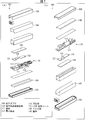
- the heat dissipation mechanism 2 of the AC adapter 1B as the electronic apparatus of the present embodiment is molded and filled as shown in FIGS. 5 (a) and 5 (b) and FIGS. 6 (a) to 6 (e).
- the material 60 is different in that the material 60 is made of a layered sheet-like material.
- FIG. 5A shows the configuration of the heat dissipation mechanism 2 of the AC adapter 1B in the present embodiment, and is an exploded perspective view of the AC adapter 1B as viewed from below.
- FIG. 5B shows the structure of the heat dissipation mechanism 2 of the AC adapter 1B, and is an exploded perspective view of the AC adapter 1B as viewed from above.
- FIGS. 6A to 6E are plan views showing configurations of the first sheet 61 to the fifth sheet 65 in the molding filler 60 of the AC adapter 1B.
- a molded filler as a filler.
- Reference numeral 60 is made of a sheet material stacked in layers.
- the protrusion 13 such as the surface mounting component mounted on the back surface of the electronic component mounting substrate 10 has a complicated unevenness in the height direction. There is. In that case, it is difficult to form the hole 21 having unevenness in a complicated manner in the height direction with the molding filler 20 of Embodiment 1 composed of one piece.
- the molding filler 60 of the present embodiment is formed by laminating the first sheet 61 to the fifth sheet 65 as sheet-like materials. ing.
- Each of the first sheet 61 to the fifth sheet 64 has a first sheet hole in accordance with the shape of the protrusion 13 such as the surface mounting component mounted on the back surface of the electronic component mounting substrate 10 in the height direction.
- a portion 61a, a second sheet hole 62a, a third sheet hole 63, and a fourth sheet hole 64a are formed.
- the first sheet hole portion 61a, the second sheet hole portion 62a, the third sheet hole portion 63, and the fourth sheet hole portion 64a of each of the first sheet 61 to the fifth sheet 64 are the protruding portions 13 at the height positions where they overlap.
- the die is molded according to the shape including the size.
- the first sheet 61 to the fifth sheet 65 are sequentially stacked on the back surface of the electronic component mounting substrate 10.
- the protruding portion 13 such as the surface mounting component mounted on the back surface of the electronic component mounting substrate 10 has a complicated unevenness in the height direction, it protrudes for each of the first sheet 61 to the fifth sheet 64.
- the first sheet hole 61a, the second sheet hole 62a, the third sheet hole 63, and the fourth sheet hole 64a can be easily formed according to the shape of the portion 13.
- the present invention when the molding filler 60 is inserted into the gap 3, the first sheet 61 to the fifth sheet 65 are sequentially stacked on the back surface of the electronic component mounting board 10.
- the present invention is not necessarily limited to this, and it is possible to insert the first sheet 61 to the fifth sheet 65, which are previously stacked and integrated with an adhesive or the like, at a time.
- each of the first sheet 61 to the fifth sheet 65 is made of a material having elasticity or plasticity that is deformed when pressed by the protruding portion 13.
- the first sheet 61 to the fifth sheet 65 can be made of a rubber-based material such as silicone rubber or butadiene rubber.
- the height of the protrusions 13 of the surface mount components and the attachment position may vary. obtain.
- the first sheet 61 to the fifth sheet 65 of the molded filler 60 are deformed as long as the molded filler 60 has elasticity or plasticity that is deformed when pressed by the protruding portion 13. Thus, it can be easily inserted into the gap 3 in which the protrusion 13 is formed.
- the heat dissipation mechanism 2 of the electronic device includes an electronic component mounting substrate 10 in which the electronic component 12 is mounted on the substrate 11, and a housing that houses the electronic component mounting substrate 10.
- a back side heat radiating metal plate (lower side aluminum plate 42) covering at least the back side of the electronic component mounting board 10, and a plurality of The protrusion 13 is inserted into the gap 3 between the back surface of the electronic component mounting substrate 10 on which the protrusion 13 including the soldered portion is formed and the back surface side heat radiating metal plate (lower aluminum plate 42). It is characterized by comprising a filler (molded filler 20) molded with a hole 21 matched to the shape.
- the filler is formed by molding with a hole that matches the shape of the protruding portion including a plurality of soldered portions. For this reason, even if the protrusions having various shapes and sizes exist, the electronic component mounting board on which the protrusions including a plurality of soldering parts are formed can be simply covered with the filler on the back surface of the electronic component mounting board. A filler can be inserted and filled in the gap between the back surface and the backside heat radiating metal plate.
- the filler does not consist of a plurality of members, the filler can be easily inserted and filled in the gap portion at one time. As a result, it does not take time for positioning, so the man-hour is not increased.
- the filler is molded with a hole that matches the shape of the protrusion. For this reason, it sets so that a desired clearance gap may be filled with a filler. As a result, unlike the case where a granular or lump filler that is deformed when pressure is applied is inserted, a necessary portion of the gap is not filled with the filler.
- a heat dissipation mechanism for an electronic device that can efficiently fill the gap between the back surface of the electronic component mounting board on which the protrusions including the plurality of soldering portions are formed and the back surface side heat radiating metal plate. be able to.
- the heat dissipating mechanism 2 of the electronic device (AC adapter 1A / AC adapter 1B) according to aspect 2 of the present invention is the heat dissipating mechanism of the electronic device according to aspect 1, wherein the filler (molded filler 20 / molded filler 60) is It is preferable to be deformed when pressed by the protrusion 13.
- the protruding portion of the surface mounting component or the like may vary in height or mounting position.
- the filler can be easily inserted by being deformed.
- the heat dissipating mechanism 2 of the electronic device (AC adapter 1B) in aspect 3 of the present invention is the heat dissipating mechanism of the electronic device in aspect 1 or 2, wherein the filler (molded filler 60) is a sheet-like material (first sheet 61). To the fifth sheet 65), and each sheet-like material (first sheet 61 to fifth sheet 65) is shaped according to the shape of the protruding portion 13 at the height of the sheet. It is preferable that the sheet is punched (one sheet hole 61a, second sheet hole 62a, third sheet hole 63, fourth sheet hole 64a).
- the heat dissipating mechanism 2 of the electronic device (AC adapter 1A / AC adapter 1B) according to aspect 4 of the present invention is the heat dissipating mechanism of the electronic device according to aspect 1, 2, or 3, wherein the back surface heat dissipating metal plate (lower aluminum plate 42) Is preferably made of an aluminum plate.
- the aluminum plate has high thermal conductivity, so the heat generated by the electronic components mounted on the electronic component mounting board can be efficiently dissipated to the housing via the backside heat dissipation metal plate made of aluminum plate. Can do.
- a power supply device (AC adapter 1A / AC adapter 1B) according to aspect 5 of the present invention includes the heat dissipation mechanism 2 for an electronic device according to any one of aspects 1 to 4.
- an electronic device that can efficiently fill the gap between the back surface of the electronic component mounting board on which the protruding portion including the plurality of soldering portions is formed and the heat radiation metal plate on the back surface can be efficiently filled.
- a power supply device including a heat dissipation mechanism can be provided.
- the present invention can be applied to an electronic device including an electronic component mounting board in which an electronic component is mounted on a board, and a housing that houses the electronic component mounting board. Moreover, as an electronic device, it can apply to power supply devices, such as an AC adapter and a switching power supply circuit, for example.
Landscapes
- Engineering & Computer Science (AREA)
- Microelectronics & Electronic Packaging (AREA)
- Physics & Mathematics (AREA)
- Thermal Sciences (AREA)
- Cooling Or The Like Of Electrical Apparatus (AREA)
- Cooling Or The Like Of Semiconductors Or Solid State Devices (AREA)
Abstract
La présente invention concerne un adaptateur CA (1A) qui est pourvu d'un substrat de montage de composant électronique (10) dans lequel des composants électroniques (12) sont installés sur un substrat (11), et un boîtier supérieur (51) et un boîtier inférieur (52) dans lesquels est logé le substrat de montage de composant électronique (10). L'invention concerne un mécanisme de rayonnement thermique (2) qui est pourvu de : une plaque d'aluminium côté inférieur (42) qui recouvre au moins le côté arrière du substrat de montage de composant électronique (10) ; et un matériau de charge moulé (20) pour insertion dans une partie d'espacement entre la plaque d'aluminium côté inférieur (42) et le côté arrière du substrat de montage de composant électronique (10) où des parties saillantes (13) comprenant une pluralité de parties soudées ont été formées, ledit matériau de charge moulé (20) étant moulé de manière à avoir des parties d'ouvertures (21) qui correspondent aux formes des parties saillantes (13).
Applications Claiming Priority (2)
| Application Number | Priority Date | Filing Date | Title |
|---|---|---|---|
| JP2014-066870 | 2014-03-27 | ||
| JP2014066870 | 2014-03-27 |
Publications (1)
| Publication Number | Publication Date |
|---|---|
| WO2015146257A1 true WO2015146257A1 (fr) | 2015-10-01 |
Family
ID=54194799
Family Applications (1)
| Application Number | Title | Priority Date | Filing Date |
|---|---|---|---|
| PCT/JP2015/051713 Ceased WO2015146257A1 (fr) | 2014-03-27 | 2015-01-22 | Mécanisme de rayonnement thermique pour appareil électronique et dispositif d'alimentation |
Country Status (1)
| Country | Link |
|---|---|
| WO (1) | WO2015146257A1 (fr) |
Citations (4)
| Publication number | Priority date | Publication date | Assignee | Title |
|---|---|---|---|---|
| JPS55159598U (fr) * | 1979-05-02 | 1980-11-15 | ||
| JPH0361387U (fr) * | 1989-05-31 | 1991-06-17 | ||
| JP2002203425A (ja) * | 2000-12-28 | 2002-07-19 | Matsushita Electric Works Ltd | 放電灯点灯装置 |
| JP2008135668A (ja) * | 2006-11-29 | 2008-06-12 | Mitsumi Electric Co Ltd | 電子機器の筐体構造及び電源装置 |
-
2015
- 2015-01-22 WO PCT/JP2015/051713 patent/WO2015146257A1/fr not_active Ceased
Patent Citations (4)
| Publication number | Priority date | Publication date | Assignee | Title |
|---|---|---|---|---|
| JPS55159598U (fr) * | 1979-05-02 | 1980-11-15 | ||
| JPH0361387U (fr) * | 1989-05-31 | 1991-06-17 | ||
| JP2002203425A (ja) * | 2000-12-28 | 2002-07-19 | Matsushita Electric Works Ltd | 放電灯点灯装置 |
| JP2008135668A (ja) * | 2006-11-29 | 2008-06-12 | Mitsumi Electric Co Ltd | 電子機器の筐体構造及び電源装置 |
Similar Documents
| Publication | Publication Date | Title |
|---|---|---|
| US7180745B2 (en) | Flip chip heat sink package and method | |
| US10194523B2 (en) | Circuit assembly, electrical junction box, and manufacturing method for circuit assembly | |
| US20120147565A1 (en) | Heat dissipation and temperature-homogenizing structure and electronic device having the same | |
| US8619428B2 (en) | Electronic package structure | |
| US10418177B2 (en) | Capacitor with improved heat dissipation | |
| US9795053B2 (en) | Electronic device and method for manufacturing the electronic device | |
| TWI552358B (zh) | 包含一太陽光電模板之太陽光電系統內所用之一種二極體單元模組 | |
| CN108352691B (zh) | 电路结构体及电气接线盒 | |
| CN111373525B (zh) | 电路结构体及电接线盒 | |
| US20220254765A1 (en) | Power structure, preparation method, and device | |
| JP2020178406A (ja) | 電力変換装置 | |
| JP4433875B2 (ja) | 発熱部品の放熱構造と、この放熱構造における放熱部材の製造方法 | |
| US20150194816A1 (en) | Electrically powered portable device | |
| TW201204227A (en) | Heat dissipation apparatus | |
| WO2019216366A1 (fr) | Structure de circuit | |
| JP5611116B2 (ja) | 電源装置 | |
| CN107078106A (zh) | 散热结构 | |
| WO2015146257A1 (fr) | Mécanisme de rayonnement thermique pour appareil électronique et dispositif d'alimentation | |
| CN106463487B (zh) | 具有导热装置的电子模块和制造电子模块的方法 | |
| CN112823416A (zh) | 表面安装式热缓冲器 | |
| WO2016104110A1 (fr) | Structure de circuit et boîtier de jonction électrique | |
| CN211557841U (zh) | 具有倒扣式散热结构的户外移动电源及倒扣式散热器结构 | |
| CN214848623U (zh) | 电控板 | |
| CN205847838U (zh) | 一种具有散热装置的电子装置 | |
| CN207611764U (zh) | 高散热的mos器件以及电子设备 |
Legal Events
| Date | Code | Title | Description |
|---|---|---|---|
| 121 | Ep: the epo has been informed by wipo that ep was designated in this application |
Ref document number: 15770405 Country of ref document: EP Kind code of ref document: A1 |
|
| NENP | Non-entry into the national phase |
Ref country code: DE |
|
| 122 | Ep: pct application non-entry in european phase |
Ref document number: 15770405 Country of ref document: EP Kind code of ref document: A1 |
|
| NENP | Non-entry into the national phase |
Ref country code: JP |