WO2015146643A1 - Capteur d'image et dispositif électronique - Google Patents
Capteur d'image et dispositif électronique Download PDFInfo
- Publication number
- WO2015146643A1 WO2015146643A1 PCT/JP2015/057529 JP2015057529W WO2015146643A1 WO 2015146643 A1 WO2015146643 A1 WO 2015146643A1 JP 2015057529 W JP2015057529 W JP 2015057529W WO 2015146643 A1 WO2015146643 A1 WO 2015146643A1
- Authority
- WO
- WIPO (PCT)
- Prior art keywords
- frame
- image data
- buffer
- memory
- image sensor
- Prior art date
- Legal status (The legal status is an assumption and is not a legal conclusion. Google has not performed a legal analysis and makes no representation as to the accuracy of the status listed.)
- Ceased
Links
Images





Classifications
-
- H—ELECTRICITY
- H04—ELECTRIC COMMUNICATION TECHNIQUE
- H04N—PICTORIAL COMMUNICATION, e.g. TELEVISION
- H04N23/00—Cameras or camera modules comprising electronic image sensors; Control thereof
- H04N23/60—Control of cameras or camera modules
- H04N23/667—Camera operation mode switching, e.g. between still and video, sport and normal or high- and low-resolution modes
-
- H—ELECTRICITY
- H04—ELECTRIC COMMUNICATION TECHNIQUE
- H04N—PICTORIAL COMMUNICATION, e.g. TELEVISION
- H04N25/00—Circuitry of solid-state image sensors [SSIS]; Control thereof
- H04N25/40—Extracting pixel data from image sensors by controlling scanning circuits, e.g. by modifying the number of pixels sampled or to be sampled
- H04N25/42—Extracting pixel data from image sensors by controlling scanning circuits, e.g. by modifying the number of pixels sampled or to be sampled by switching between different modes of operation using different resolutions or aspect ratios, e.g. switching between interlaced and non-interlaced mode
Definitions
- the present disclosure relates to an image sensor and an electronic device, and more particularly, to an image sensor and an electronic device that can output a dummy frame instead of a defective frame that may be caused by a change in a reading mode.
- the change of the readout mode in the image sensor involves the change of the shutter speed (exposure time) and the readout time of pixel data (hereinafter also referred to as a frame), the exposure time of each pixel is changed at the timing when the readout mode is changed. This results in defective frames that are not unified and cannot be used as images.
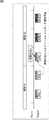
- FIG. 1 shows a conventional method for dealing with defective frames.
- a defective frame that can be generated when read mode A (MODE-A) is changed to read mode B (MODE-B) is output to the subsequent stage. It is a way not to.
- the first coping method only frames that can always be used as images can be output to the subsequent stage.
- the frame output is interrupted by one frame, and there is a request to continue the frame output as much as possible. Therefore, there is a second target method that responds to the request. .
- frames that can be used as images can be output continuously. However, in this case, the frame rate is temporarily lost.
- the present disclosure has been made in view of such a situation, and allows a frame that can be used as an image to be continuously output without breaking the frame rate.
- An image sensor has a plurality of readout modes, a pixel unit that generates image data according to incident light, and a memory having a capacity capable of storing at least two frames of the image data.
- a control unit that simultaneously performs a process of storing the image data input from the pixel unit in a different area of the memory for each frame, and a process of reading the image data from the previously stored area, and the reading of the pixel unit
- a detection unit that detects a change in mode.
- the control unit can stop the process of storing the image data input from the pixel unit in the memory when the change of the readout mode is detected by the detection unit.
- the control unit can perform a process of rereading the read image data from an area where the image data was previously stored in the memory when the change of the read mode is detected by the detection unit.
- the memory may include a first buffer and a second buffer that can store the image data for one frame, and the control unit may store the image data input from the pixel unit for each frame.
- a process of storing in one of the first buffer or the second buffer and a process of reading the image data from the other of the first buffer or the second buffer can be performed simultaneously.
- An electronic device has a plurality of readout modes, a pixel unit that generates image data according to incident light, and a capacity that can store at least two frames of the image data.
- a memory a control unit that simultaneously stores the image data input from the pixel unit in a different area of the memory for each frame, and a process of reading the image data from the previously stored area;
- An image sensor including a detection unit that detects a change in the readout mode is mounted.
- a process of storing image data input from the pixel unit in different areas of the memory for each frame and a process of reading the image data from the previously stored area are performed simultaneously. . Furthermore, a change in the readout mode of the pixel portion is detected.
- FIG. 2 shows an outline of the operation of the image sensor according to the embodiment of the present disclosure.
- the image sensor like the conventional image sensor described above, switches a plurality of readout modes (addition readout mode, HDR readout mode, etc.) during imaging and outputs a frame to the subsequent stage.
- a plurality of readout modes additional readout mode, HDR readout mode, etc.
- the image sensor is already output in the memory (multiple frame storage memory 13 in FIG. 3) stored in the image sensor instead of outputting the defective frame that can be generated at the timing when the readout mode is changed to the subsequent stage.
- the already-completed frame is read again as a dummy frame and output. Accordingly, the image sensor can continuously output frames that can be used as images without breaking the frame rate.
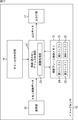
- FIG. 3 illustrates a configuration example of an image sensor that is an embodiment of the present disclosure.
- the image sensor 10 includes a pixel unit 11, a storage / readout address control unit 12, a multiple frame storage memory 13, a dummy output determination unit 16, and an output I / F unit 17.
- the pixel unit 11 has a large number of light receiving elements arranged vertically and horizontally, and stores / reads out a pixel signal generated according to incident light in each light receiving element as memory storage data for each row according to a predetermined frame rate. Output to the control unit 12. It is assumed that the shutter speed (exposure time) of each light receiving element in the pixel unit 11 and the readout time of the generated pixel signal change according to the set readout mode.
- the storage / read-out address control unit 12 can individually control the storage address and the read-out address for the multiple-frame storage memory 13, and can store memory storage data (hereinafter also referred to as a frame) from the pixel unit 11 in the multiple-frame storage memory. 13 and the process of reading the frame stored in the multiple frame storage memory 13 and outputting it to the output I / F unit 17 are executed simultaneously. Further, the storage / reading address control unit 12 can perform front-end processing on the memory storage data from the pixel unit 11 and back-end processing on the memory storage data stored in the plural-frame storage memory 13.
- the storage / reading address control unit 12 responds to the notification from the dummy output determination unit 16, and the first buffer 14 and the second buffer 14 of the multiple-frame storage memory 13 for defective frames that can be input from the pixel unit 11 as memory storage data. Stop storing in the buffer 15.
- the storage / read address control unit 12 may be separated into a storage address control unit and a read address control unit.
- the multi-frame storage memory 13 has a capacity capable of storing memory storage data for at least two frames.
- the multiple-frame storage memory 13 includes a first buffer 14 and a second buffer 15 each having a capacity for one frame.
- the storage / read address control unit 12 stores the memory storage data in one of the first buffer 14 or the second buffer 15 of the multi-frame storage memory 13 and reads the memory storage data from the other and outputs it. Processing to be output to the I / F unit 17 can be executed simultaneously. Further, the storage / read address control unit 12 stores the memory storage data in the first buffer 14 of the multi-frame storage memory 13, reads the memory storage data from the first buffer 14, and outputs the output I / F unit 17. Can be executed simultaneously. The same applies to the second buffer 15.
- the dummy output determination unit 16 detects a change in the read mode of the image sensor 10 in which a defective frame can be input from the pixel unit 11 and notifies the storage / read address control unit 12 of the detection result.
- the output I / F unit 17 outputs the frame input as output data from the storage / read address control unit 12 to the subsequent stage.
- FIG. 4 shows a state of control of the storage / read address control unit 12 when the Nth frame is input from the pixel unit 11 and when the (N + 1) th frame is input.
- the storage / read address control unit 12 converts the Nth frame into the first buffer 14 or the second buffer 15 of the multiple frame storage memory 13 as shown in FIG. Of these, the data is stored in the other (first buffer 14) different from the previously stored one. At the same time, the frame stored in one (second buffer 15) stored last time is read out.
- the storage / read address control unit 12 converts the (N + 1) th frame into the first buffer 14 or the second frame of the multiple-frame storage memory 13 as shown in FIG.
- the buffer 15 is stored in the other (second buffer 15) different from the previously stored one.
- the frame stored in one (first buffer 14) stored last time is read out.
- the storage / read address control unit 12 stores frames alternately in the first buffer 14 and the second buffer 15 of the multiple frame storage memory 13. Then, reading is performed from the one not storing the frame this time (the one stored last time).
- FIG. 5 shows a state of control of the storage / read address control unit 12 when the dummy output determination unit 16 detects a change in the read mode of the image sensor 10.
- a defective frame can be input from the pixel unit 11 as shown in FIG. 5A, and the storage / reading address control unit 12 uses this as the first buffer 14 and the second buffer. 15 is not stored. However, the frame stored in the last stored one (in this case, the second buffer 15) is read.
- the storage / read address control unit 12 assigns the frame to the first buffer 14 or the second buffer 15 of the multiple frame storage memory 13. Then, the data is stored in the other (first buffer 14) different from the previously stored one. At the same time, the already read frame stored in one (second buffer 15) stored previously is read again as a dummy frame.
- the same frame may be output continuously by the control of the storage / read address control unit 12 described above, it is possible to continuously output frames that can be used as images without breaking the frame rate. it can.
- FIG. 6 is a flowchart for explaining frame output processing of the image sensor 10.
- memory storage data (however, it may be a defective frame) is input from the pixel unit 11 to the storage / readout address control unit 12 at a predetermined frame rate. Executed for each frame.
- step S1 when the dummy output determination unit 16 detects a change in the reading mode of the image sensor 10, a notification indicating that is output to the storage / reading address control unit 12.
- the storage / read address control unit 12 advances the process to step S ⁇ b> 2 when there is no notification of the change of the read mode from the dummy output determination unit 16, that is, when there is no change of the read mode.
- step S ⁇ b> 2 the storage / readout address control unit 12 stores the frame input from the pixel unit 11 last time in the first buffer 14 or the second buffer 15 of the multiple frame storage memory 13 (for example, the second buffer). The data is stored in the other (the first buffer 14 in this example) different from the buffer 15. At the same time, the storage / read address control unit 12 reads out the frame stored in the previous stored one (second buffer 15 in the present example) and outputs it to the output I / F unit 17 in step S3.
- step S4 the output I / F unit 17 outputs the frame input from the storage / read address control unit 12 to the subsequent stage.
- Step S1 the next frame input from the pixel unit 11 is set as a processing target, and the steps after Step S1 are repeated.
- step S1 when the dummy output determination unit 16 detects a change in the reading mode of the image sensor 10 and notifies the storage / reading address control unit 12 to that effect, the storage / reading address control unit 12 Step S2 is skipped and the process proceeds to step S3. That is, the storage / reading address control unit 12 does not store the defective frame input from the pixel unit 11 in either the first buffer 14 or the second buffer 15 and performs only reading.
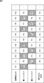
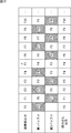
- FIG. 7 shows an example of the result of the frame output process described above.
- frames F0, F1, F2,... are sequentially input from the pixel unit 11 to the storage / readout address control unit 12.
- the frame F5 is a defective frame.
- the mesh pattern in the figure means that the frame is stored in the buffer.
- the frame F2 when the frame F2 is input, it is stored in the first buffer 14, and at the same time, the frame F1 is read from the second buffer 15 and output.
- the frame F3 when the frame F3 is input, it is stored in the second buffer 15, and at the same time, the frame F2 is read from the first buffer 14 and output.
- the frame F4 when the frame F4 is input, it is stored in the first buffer 14, and at the same time, the frame F3 is read from the second buffer 15 and output.
- the defective frame F5 when the defective frame F5 is input, it is not stored in either the first buffer 14 or the second buffer 15, and the frame F4 is read out from the first buffer 14 that was previously stored and output. Is done.
- the frame F6 when the frame F6 is inputted, it is stored in the second buffer 15, and at the same time, the frame F3 is read again from the first buffer 14 and outputted. Thereafter, storage and reading are performed at the same time.
- the frame F3 may be read again from the second buffer 15 and output.
- ⁇ Other examples of frame output processing> 10 and 11 show the state of another operation example of the frame output process
- FIG. 12 shows an example of the result of the other operation example of the frame output process.
- FAST AF is realized by Contrast AF, and the focus is determined based on a plurality of frames (about 30 frames) obtained by a high-speed shutter of about 120 fps while changing the focus.
- the preview display is started after FAST AF is performed immediately after startup, and the frame is in a state where the focus is determined again by FAST AF being performed according to the shutter operation performed while the user is viewing the preview display. Is output and recorded in the subsequent stage.
- the image sensor could not output a preview frame (thinned out) to the subsequent stage, and the preview display was blacked out.
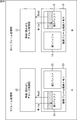
- the image sensor 10 according to the present embodiment can realize a preview display even during FAST AF. Specifically, this is as shown in FIGS.
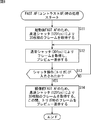
- FIG. 8 is a flowchart for explaining processing during FAST AF by the image sensor 10.
- FIG. 9 is a diagram supplementing FIG. 8, and symbols (S11, etc.) in the diagram correspond to the processing steps of FIG.
- step S11 for FAST AF after startup, multiple frames (about 30 frames) are acquired with a high-speed shutter (about 120 fps) while changing focus, and output to the subsequent stage.
- step S12 a preview display frame is acquired with a normal shutter (30 fps) and output to the subsequent stage. At this time, a preview frame is alternately stored and read in the first buffer 14 and the second buffer 15 of the plural-frame storage memory 13.
- step S13 the presence or absence of the shutter operation is confirmed, and steps S12 and S13 are repeated until the shutter operation is performed. If there is a shutter operation, the process proceeds to step S14.
- step S14 about 30 frames are acquired with a high-speed shutter while changing the focus for FAST AF for imaging, and output to the subsequent stage. At this time, the preview frame remaining in the first buffer 14 or the second buffer 15 is read again and output to the subsequent stage.
- the imaging apparatus equipped with the image sensor 10 can continue the preview display even at the time of FAST AF and prevent blackout.
- image sensor 10 ⁇ Application example of image sensor 10>
- the image sensor 10 according to the present embodiment described above can be applied to any electronic device having an imaging function or a sensing function.
- FIG. 13 shows another configuration example of the image sensor 10 according to the present embodiment.
- an image processing unit 21 that performs predetermined image processing may be provided inside the storage / read address control unit 12.
- the storage / read address control unit 12 may execute a plurality of storage address controls and a plurality of read address controls.
- a larger number of buffers (in the case of the figure, the third buffer 22 and the fourth buffer 23) may be provided in the multiple frame storage memory 13.
- this indication can also take the following structures.
- a pixel unit having a plurality of readout modes and generating image data according to incident light;
- a memory having a capacity capable of storing the image data of at least two frames or more;
- a control unit that simultaneously performs a process of storing the image data input from the pixel unit in a different area of the memory for each frame, and a process of reading the image data from the previously stored area;
- An image sensor comprising: a detection unit that detects a change in the readout mode of the pixel unit.
- the said control part stops the process which stores the said image data input from the said pixel part in the said memory, when the change of the said reading mode is detected by the said detection part.
- the image sensor as described in said (1).
- the control unit stops the process of storing the image data of the defective frame input from the pixel unit in the memory when the detection unit detects a change in the readout mode.
- (1) or (2) The image sensor described in 1.
- the control unit performs a process of reading the image data that has been read again from an area in which the image data was previously stored in the memory.
- the image sensor according to any one of (3).
- the memory includes a first buffer and a second buffer that can store the image data for one frame, The control unit stores the image data input from the pixel unit in one of the first buffer and the second buffer of the memory for each frame, and the other of the first buffer and the second buffer.
- the image sensor according to any one of (1) to (4), wherein a process of reading the image data from is simultaneously performed.
- a pixel unit having a plurality of readout modes and generating image data according to incident light;
- a memory having a capacity capable of storing the image data of at least two frames or more;
- a control unit that simultaneously performs a process of storing the image data input from the pixel unit in a different area of the memory for each frame, and a process of reading the image data from the previously stored area;
- An electronic device equipped with an image sensor comprising: a detection unit that detects a change in the readout mode of the pixel unit.
Landscapes
- Engineering & Computer Science (AREA)
- Multimedia (AREA)
- Signal Processing (AREA)
- Transforming Light Signals Into Electric Signals (AREA)
- Studio Devices (AREA)
Abstract
La présente invention concerne un capteur d'image qui permet une sortie continue de trames qui peuvent être utilisées comme images sans perturber la fréquence de trames, et un dispositif électronique. Un capteur d'image, selon un aspect de la présente invention, comporte : une unité de pixel qui a une pluralité de modes de lecture et génère des données d'image en réponse à la lumière incidente ; une mémoire qui a une capacité capable de stocker les données d'image correspondant à au moins deux trames ou plus ; une unité de commande qui exécute simultanément un traitement pour stocker les données d'image entrées à partir de l'unité de pixel trame par trame dans une région différente de la mémoire et un traitement pour lire les données d'image provenant d'une région pour le dernier stockage ; et une unité de détection qui détecte le changement du mode de lecture de l'unité de pixel. La présente invention est applicable à un dispositif électronique comportant une fonction de capture d'image.
Priority Applications (1)
| Application Number | Priority Date | Filing Date | Title |
|---|---|---|---|
| US15/125,746 US10306159B2 (en) | 2014-03-26 | 2015-03-13 | Continuous output of frames with constant frame rate |
Applications Claiming Priority (2)
| Application Number | Priority Date | Filing Date | Title |
|---|---|---|---|
| JP2014-064008 | 2014-03-26 | ||
| JP2014064008A JP2015186234A (ja) | 2014-03-26 | 2014-03-26 | イメージセンサ、および電子装置 |
Publications (1)
| Publication Number | Publication Date |
|---|---|
| WO2015146643A1 true WO2015146643A1 (fr) | 2015-10-01 |
Family
ID=54195166
Family Applications (1)
| Application Number | Title | Priority Date | Filing Date |
|---|---|---|---|
| PCT/JP2015/057529 Ceased WO2015146643A1 (fr) | 2014-03-26 | 2015-03-13 | Capteur d'image et dispositif électronique |
Country Status (3)
| Country | Link |
|---|---|
| US (1) | US10306159B2 (fr) |
| JP (1) | JP2015186234A (fr) |
| WO (1) | WO2015146643A1 (fr) |
Families Citing this family (2)
| Publication number | Priority date | Publication date | Assignee | Title |
|---|---|---|---|---|
| JP7840667B2 (ja) | 2021-11-25 | 2026-04-06 | キヤノン株式会社 | 電子機器及びその制御方法、及び撮像装置及びその制御方法 |
| CN115225841A (zh) * | 2022-07-18 | 2022-10-21 | 芯原微电子(上海)股份有限公司 | 一种时序控制器、图像处理系统及图像处理方法 |
Citations (3)
| Publication number | Priority date | Publication date | Assignee | Title |
|---|---|---|---|---|
| JP2006197097A (ja) * | 2005-01-12 | 2006-07-27 | Canon Inc | 固体撮像素子 |
| JP2012054876A (ja) * | 2010-09-03 | 2012-03-15 | Sony Corp | 固体撮像素子およびカメラシステム |
| JP2012151787A (ja) * | 2011-01-21 | 2012-08-09 | Nec Casio Mobile Communications Ltd | 撮像装置及び電子ズーム方法 |
Family Cites Families (3)
| Publication number | Priority date | Publication date | Assignee | Title |
|---|---|---|---|---|
| KR100674712B1 (ko) * | 2005-08-05 | 2007-01-25 | 삼성전기주식회사 | Ddr을 이용한 데이터의 스캔 시스템 또는 방법 |
| JP4765578B2 (ja) | 2005-11-24 | 2011-09-07 | ソニー株式会社 | 固体撮像素子とその駆動方法、及びカメラモジュール |
| JP5188080B2 (ja) * | 2007-03-06 | 2013-04-24 | キヤノン株式会社 | 撮像装置、撮像装置の駆動方法、及び読み出し装置 |
-
2014
- 2014-03-26 JP JP2014064008A patent/JP2015186234A/ja active Pending
-
2015
- 2015-03-13 US US15/125,746 patent/US10306159B2/en active Active
- 2015-03-13 WO PCT/JP2015/057529 patent/WO2015146643A1/fr not_active Ceased
Patent Citations (3)
| Publication number | Priority date | Publication date | Assignee | Title |
|---|---|---|---|---|
| JP2006197097A (ja) * | 2005-01-12 | 2006-07-27 | Canon Inc | 固体撮像素子 |
| JP2012054876A (ja) * | 2010-09-03 | 2012-03-15 | Sony Corp | 固体撮像素子およびカメラシステム |
| JP2012151787A (ja) * | 2011-01-21 | 2012-08-09 | Nec Casio Mobile Communications Ltd | 撮像装置及び電子ズーム方法 |
Also Published As
| Publication number | Publication date |
|---|---|
| JP2015186234A (ja) | 2015-10-22 |
| US10306159B2 (en) | 2019-05-28 |
| US20170013208A1 (en) | 2017-01-12 |
Similar Documents
| Publication | Publication Date | Title |
|---|---|---|
| KR102229152B1 (ko) | 이미지 촬영 장치 | |
| JP6652039B2 (ja) | 撮像装置、撮像方法及びプログラム | |
| JP2008129554A (ja) | 撮像装置及びオートフォーカス制御方法 | |
| US20130120642A1 (en) | Digital photographing apparatus and method of controlling the same | |
| US8416320B2 (en) | Image processing method and apparatus for generating and displaying screen nail images | |
| US9363440B2 (en) | Imaging device and imaging method that sets a phase difference between first and second synchronization signals | |
| EP3065128B1 (fr) | Dispositif d'imagerie | |
| US20130076973A1 (en) | Image pickup apparatus, control method therefor, and storage medium storing control program therefor | |
| US20120057038A1 (en) | Imaging apparatus, readout control method, program product, readout control apparatus, and solid-state imaging device | |
| JP5530262B2 (ja) | 手振れ補正制御装置、手振れ補正制御方法、撮像装置およびプログラム | |
| WO2015146643A1 (fr) | Capteur d'image et dispositif électronique | |
| US9253401B2 (en) | Imaging device and imaging method where shake adjusted image is divided into regions for parallel processing | |
| JP2013135410A (ja) | 撮像装置および評価値生成装置 | |
| CN116132805B (zh) | 成像元件、摄像装置、成像元件的工作方法及存储介质 | |
| JP7461732B2 (ja) | 撮像装置及びその制御方法、プログラム、記憶媒体 | |
| US9288397B2 (en) | Imaging device, method for processing image, and program product for processing image | |
| US20140308018A1 (en) | Image capturing apparatus and method of controlling the same | |
| US20120127344A1 (en) | Image pickup device | |
| US11202015B2 (en) | Control apparatus and control method | |
| JP7087187B2 (ja) | ぶれ補正装置、撮像装置、監視システム、及びプログラム | |
| US20150206274A1 (en) | Image processing apparatus, image processing method, and storage medium storing program | |
| JP2018054762A5 (fr) | ||
| JP6569188B2 (ja) | 撮像装置 | |
| JP5874473B2 (ja) | 電子カメラ | |
| JP2008016961A (ja) | 撮像装置および読出制御方法 |
Legal Events
| Date | Code | Title | Description |
|---|---|---|---|
| 121 | Ep: the epo has been informed by wipo that ep was designated in this application |
Ref document number: 15769067 Country of ref document: EP Kind code of ref document: A1 |
|
| WWE | Wipo information: entry into national phase |
Ref document number: 15125746 Country of ref document: US |
|
| NENP | Non-entry into the national phase |
Ref country code: DE |
|
| 122 | Ep: pct application non-entry in european phase |
Ref document number: 15769067 Country of ref document: EP Kind code of ref document: A1 |