WO2015146975A1 - Dispositif électronique - Google Patents
Dispositif électronique Download PDFInfo
- Publication number
- WO2015146975A1 WO2015146975A1 PCT/JP2015/058904 JP2015058904W WO2015146975A1 WO 2015146975 A1 WO2015146975 A1 WO 2015146975A1 JP 2015058904 W JP2015058904 W JP 2015058904W WO 2015146975 A1 WO2015146975 A1 WO 2015146975A1
- Authority
- WO
- WIPO (PCT)
- Prior art keywords
- electronic device
- flexible tube
- sealed space
- flexible
- seal structure
- Prior art date
- Legal status (The legal status is an assumption and is not a legal conclusion. Google has not performed a legal analysis and makes no representation as to the accuracy of the status listed.)
- Ceased
Links
Images

Classifications
-
- H—ELECTRICITY
- H01—ELECTRIC ELEMENTS
- H01B—CABLES; CONDUCTORS; INSULATORS; SELECTION OF MATERIALS FOR THEIR CONDUCTIVE, INSULATING OR DIELECTRIC PROPERTIES
- H01B1/00—Conductors or conductive bodies characterised by the conductive materials; Selection of materials as conductors
- H01B1/04—Conductors or conductive bodies characterised by the conductive materials; Selection of materials as conductors mainly consisting of carbon-silicon compounds, carbon or silicon
-
- H—ELECTRICITY
- H10—SEMICONDUCTOR DEVICES; ELECTRIC SOLID-STATE DEVICES NOT OTHERWISE PROVIDED FOR
- H10K—ORGANIC ELECTRIC SOLID-STATE DEVICES
- H10K10/00—Organic devices specially adapted for rectifying, amplifying, oscillating or switching; Organic capacitors or resistors having potential barriers
- H10K10/80—Constructional details
- H10K10/88—Passivation; Containers; Encapsulations
-
- H—ELECTRICITY
- H10—SEMICONDUCTOR DEVICES; ELECTRIC SOLID-STATE DEVICES NOT OTHERWISE PROVIDED FOR
- H10K—ORGANIC ELECTRIC SOLID-STATE DEVICES
- H10K30/00—Organic devices sensitive to infrared radiation, light, electromagnetic radiation of shorter wavelength or corpuscular radiation
- H10K30/80—Constructional details
- H10K30/88—Passivation; Containers; Encapsulations
-
- H—ELECTRICITY
- H10—SEMICONDUCTOR DEVICES; ELECTRIC SOLID-STATE DEVICES NOT OTHERWISE PROVIDED FOR
- H10K—ORGANIC ELECTRIC SOLID-STATE DEVICES
- H10K50/00—Organic light-emitting devices
- H10K50/80—Constructional details
- H10K50/84—Passivation; Containers; Encapsulations
- H10K50/841—Self-supporting sealing arrangements
-
- H—ELECTRICITY
- H10—SEMICONDUCTOR DEVICES; ELECTRIC SOLID-STATE DEVICES NOT OTHERWISE PROVIDED FOR
- H10K—ORGANIC ELECTRIC SOLID-STATE DEVICES
- H10K50/00—Organic light-emitting devices
- H10K50/80—Constructional details
- H10K50/84—Passivation; Containers; Encapsulations
- H10K50/842—Containers
- H10K50/8426—Peripheral sealing arrangements, e.g. adhesives, sealants
-
- H—ELECTRICITY
- H10—SEMICONDUCTOR DEVICES; ELECTRIC SOLID-STATE DEVICES NOT OTHERWISE PROVIDED FOR
- H10K—ORGANIC ELECTRIC SOLID-STATE DEVICES
- H10K59/00—Integrated devices, or assemblies of multiple devices, comprising at least one organic light-emitting element covered by group H10K50/00
- H10K59/80—Constructional details
- H10K59/87—Passivation; Containers; Encapsulations
- H10K59/871—Self-supporting sealing arrangements
- H10K59/8722—Peripheral sealing arrangements, e.g. adhesives, sealants
-
- H—ELECTRICITY
- H10—SEMICONDUCTOR DEVICES; ELECTRIC SOLID-STATE DEVICES NOT OTHERWISE PROVIDED FOR
- H10K—ORGANIC ELECTRIC SOLID-STATE DEVICES
- H10K77/00—Constructional details of devices covered by this subclass and not covered by groups H10K10/80, H10K30/80, H10K50/80 or H10K59/80
- H10K77/10—Substrates, e.g. flexible substrates
- H10K77/111—Flexible substrates
-
- H—ELECTRICITY
- H10—SEMICONDUCTOR DEVICES; ELECTRIC SOLID-STATE DEVICES NOT OTHERWISE PROVIDED FOR
- H10K—ORGANIC ELECTRIC SOLID-STATE DEVICES
- H10K50/00—Organic light-emitting devices
- H10K50/80—Constructional details
- H10K50/84—Passivation; Containers; Encapsulations
-
- H—ELECTRICITY
- H10—SEMICONDUCTOR DEVICES; ELECTRIC SOLID-STATE DEVICES NOT OTHERWISE PROVIDED FOR
- H10K—ORGANIC ELECTRIC SOLID-STATE DEVICES
- H10K59/00—Integrated devices, or assemblies of multiple devices, comprising at least one organic light-emitting element covered by group H10K50/00
- H10K59/80—Constructional details
- H10K59/87—Passivation; Containers; Encapsulations
-
- H—ELECTRICITY
- H10—SEMICONDUCTOR DEVICES; ELECTRIC SOLID-STATE DEVICES NOT OTHERWISE PROVIDED FOR
- H10K—ORGANIC ELECTRIC SOLID-STATE DEVICES
- H10K59/00—Integrated devices, or assemblies of multiple devices, comprising at least one organic light-emitting element covered by group H10K50/00
- H10K59/80—Constructional details
- H10K59/87—Passivation; Containers; Encapsulations
- H10K59/871—Self-supporting sealing arrangements
-
- Y—GENERAL TAGGING OF NEW TECHNOLOGICAL DEVELOPMENTS; GENERAL TAGGING OF CROSS-SECTIONAL TECHNOLOGIES SPANNING OVER SEVERAL SECTIONS OF THE IPC; TECHNICAL SUBJECTS COVERED BY FORMER USPC CROSS-REFERENCE ART COLLECTIONS [XRACs] AND DIGESTS
- Y02—TECHNOLOGIES OR APPLICATIONS FOR MITIGATION OR ADAPTATION AGAINST CLIMATE CHANGE
- Y02E—REDUCTION OF GREENHOUSE GAS [GHG] EMISSIONS, RELATED TO ENERGY GENERATION, TRANSMISSION OR DISTRIBUTION
- Y02E10/00—Energy generation through renewable energy sources
- Y02E10/50—Photovoltaic [PV] energy
- Y02E10/549—Organic PV cells
Definitions
- the present invention relates to an electronic device, and more particularly to a flexible electronic device.
- organic electronic elements of organic electronic devices are sensitive to moisture and oxygen, their performance may deteriorate due to the influence of moisture and oxygen.
- the organic electronics element is arranged on a glass substrate, covered with a sealing can, and a desiccant is enclosed. Since the glass substrate and the sealing can do not have flexibility, it is difficult to apply such an electronic device to the flexible electronic device.
- Patent Document 1 discloses a resin base material having gas barrier properties.
- the resin base material of patent document 1 forms the thin film of the inorganic oxide excellent in gas barrier property on the resin film.
- Patent Document 1 discloses an organic EL element formed on a resin base material and sealed by being covered with another resin base material.
- an electronic device in which an electronic element is sealed by bonding two resin substrates covering the electronic element may not obtain sufficient reliability.
- the location where the two resin substrates that seal the electronics elements are bonded together is inferior in water vapor barrier properties and oxygen barrier properties compared to the resin substrates themselves. For this reason, due to the water vapor and oxygen that have passed through the location where the resin base material is bonded, the performance of the electronic element may be reduced, and the reliability of the electronic device may be reduced.
- the present invention has been made in order to solve the above-described problems, and it is an object of the present invention to suppress deterioration of the performance of an electronic element due to the influence of moisture and / or oxygen and to improve the reliability of a flexible electronic device. To do.
- An electronic device includes a flexible substrate, a device portion supported by the flexible substrate, a drive circuit portion, and a water vapor permeability of less than 10 ⁇ 3 g / (m 2 ⁇ 24 h) and oxygen permeation.
- An electronic device has a flexible substrate, a device unit supported by the flexible substrate, a drive circuit unit, and a water vapor permeability of less than 10 ⁇ 3 g / (m 2 ⁇ 24 h).
- a first flexible tube having an oxygen permeability of less than 10 ⁇ 2 ml / (m 2 ⁇ 24 h ⁇ MPa) and a water vapor permeability of 10 ⁇ 3 g / (m 2) provided inside the first flexible tube.
- the first flexible tube has a sealed space between the second flexible tube and a part of the flexible substrate. Fine said device unit is located in said sealed space, a portion other than the portion of the flexible substrate outside of the sealed space.
- the sealed space is filled with an inert gas or an inert liquid having an insulating property.
- the sealed space has neither gas nor liquid.
- the drive circuit unit is in the sealed space.
- the drive circuit unit is outside the sealed space.
- a plurality of terminals connected to the device unit or the drive circuit unit are outside the sealed space.
- the electronic device further includes a control circuit unit, and the control circuit unit is in the sealed space.
- control circuit unit includes a function of contactless power reception or NFC (Near Field Communication).
- NFC Near Field Communication
- the embodiment of the present invention it is possible to suppress the deterioration of the performance of the electronic element due to the influence of moisture and / or oxygen, and to improve the reliability of the flexible electronic device.
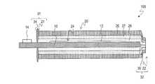
- FIG. 2 is a schematic cross-sectional view of the electronic device 100 taken along the line 2B-2B ′ in FIG. 1.
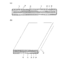
- FIG. 2A is a schematic cross-sectional view of the electronic device 100 taken along line 3B-3B ′ in FIG. 1
- FIG. 2B is a schematic perspective view of the electronic device 100.
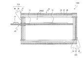
- FIG. 5 is a schematic cross-sectional view of the electronic device 100A along the line 5B-5B ′ in FIG. 4.
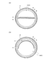
- (A) And (b) is typical sectional drawing of the electronic device 100A along the 6B-6B 'line in FIG.
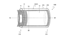
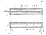
- FIG. 8 is a schematic cross-sectional view of the electronic device 100B taken along line 8B-8B ′ in FIG. 7.
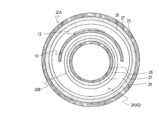
- FIG. 9 is a schematic cross-sectional view of the electronic device 100B taken along line 9B-9B ′ in FIG. 7.
- the electronic device according to the embodiment is a flexible electronic device.
- the present invention is not limited to the embodiments exemplified below.
- components having substantially the same function are denoted by common reference numerals, and description thereof may be omitted.
- FIG. 1 schematically shows an electronic device 100 according to Embodiment 1 of the present invention.
- the electronic device 100 includes a flexible substrate 10, a device unit 12 supported by the flexible substrate 10, a drive circuit unit 14, and a flexible tube 20.
- the water vapor permeability of the flexible tube 20 is less than 10 ⁇ 3 g / (m 2 ⁇ 24 h), and the oxygen permeability is less than 10 ⁇ 2 ml / (m 2 ⁇ 24 h ⁇ MPa).
- the flexible tube 20 forms a first seal structure 31 and a second seal structure 32 at both ends thereof.
- the flexible tube 20 has a sealed space 24 inside thereof. A part of the flexible substrate 10 and the device unit 12 are in the sealed space 24, and the other part of the flexible substrate 10 is outside the sealed space 24.
- the device unit 12 includes a plurality of electronic elements (not shown), and the drive circuit unit 14 includes a circuit that drives the plurality of electronic elements included in the device unit 12.
- the drive circuit unit 14 supplies a predetermined signal to the plurality of organic EL elements.
- the direction of the 2B-2B ′ line in FIG. 1 is the length direction of the flexible tube 20 or the flexible substrate 10
- the direction of the 3B-3B ′ line in FIG. 1 is the width of the flexible tube 20 or the flexible substrate 10.
- direction sometimes called direction.
- the flexible tube 20 Since the flexible tube 20 has low water vapor permeability and oxygen permeability, it is excellent in water vapor barrier properties and oxygen barrier properties.
- the sealed space 24 in the flexible tube 20 is formed by closing both ends of the flexible tube 20 by the first seal structure 31 and the second seal structure 32. Therefore, the electronic device 100 has a seal structure at the end along the width direction of the flexible tube 20, but does not have a seal structure at the end along the length direction of the flexible tube 20.
- the conventional electronic device two resin base materials are bonded together along the length direction and width direction ends of the flexible substrate.
- External moisture and oxygen mainly enter from a bonded portion (seal structure) formed along the lengthwise and widthwise ends of the flexible substrate, causing problems in the electronic device.
- the concentration of moisture and the like is high in the vicinity of the bonded portion, and also increases in the central portion in the sealed space with the passage of time. Therefore, in the conventional electronic device, a defect is likely to occur near the end along the length direction and the end along the width direction.
- the electronic device 100 does not have a seal structure at the end along the length direction of the flexible tube 20, compared to the conventional electronic device, from the end along the length direction of the flexible tube 20, The amount of moisture and oxygen entering the sealed space 24 is reduced. Since the electronic device 100 is in the space 24 in which the device unit 12 is sealed, the influence of moisture and oxygen on the electronic elements of the device unit 12 is reduced. The electronic device 100 is excellent in reliability because the performance of the electronic element is suppressed from decreasing. In particular, when the ratio of the length of the electronic device (flexible tube) to the width (aspect ratio (length / width)) is large, the effect of improving reliability is great. The relationship between the aspect ratio and the reliability of the electronic device (flexible tube) will be described later.
- FIG. 2 and 3 are a schematic sectional view and a perspective view of the electronic device 100.
- FIG. 2 is a schematic cross-sectional view taken along line 2B-2B ′ in FIG. 1
- FIG. 3A is a schematic cross-sectional view taken along line 3B-3B ′ in FIG.
- FIG. 3B is a perspective view.
- the flexible tube 20 of the electronic device 100 includes a tube base material 26, a gas barrier layer 27 inside the tube base material 26, and a seal layer 28 inside the gas barrier layer 27.
- the sealed space 24 of the electronic device 100 has neither gas nor liquid. That is, the inner surface of the flexible tube 20, a part of the flexible substrate 10 in the sealed space 24, and the device unit 12 are in close contact with each other.
- the electronic device according to the embodiment of the present invention is not limited to this.
- the sealed space 24 may be filled with an inert gas or an inert liquid having an insulating property.
- the tube base 26 of the flexible tube 20 includes, for example, polyethylene terephthalate (PET).
- PET polyethylene terephthalate
- the thickness of the tube base material 26 is, for example, 50 ⁇ m.
- the gas barrier layer 27 includes, for example, a metal, an inorganic oxide, or an inorganic nitride.
- the gas barrier layer 27 includes, for example, aluminum (Al), aluminum oxide (alumina: Al 2 O 3 ), silicon dioxide (SiO 2 ), or silicon nitride (SiN x ).
- the gas barrier layer 27 may be a single layer or may have a multilayer structure in which a plurality of layers are stacked.
- the gas barrier layer 27 may have, for example, a structure (SiO 2 / (SiN x / SiO 2 ) n / SiO 2 ) in which silicon dioxide layers and silicon nitride layers are alternately stacked and sandwiched between the silicon dioxide layers.
- the thickness of the gas barrier layer 27 is, for example, 1 ⁇ m to 2 ⁇ m.
- the gas barrier layer 27 is formed on the inside of the tube base material 26 by using, for example, a chemical vapor deposition (CVD) method, a physical vapor deposition (PVD) method, or a sputtering method. .
- CVD chemical vapor deposition
- PVD physical vapor deposition
- sputtering method a method of forming a metal, metal oxide, or ceramic thin film inside the tube.
- a method of forming a metal, metal oxide, or ceramic thin film inside the tube is disclosed in, for example, Japanese Patent No. 4945860.
- the gas barrier layer 27 is formed of an inorganic oxide (for example, alumina)
- the gas barrier layer 27 may be formed using an atomic layer deposition (ALD) method.
- ALD atomic layer deposition
- the gas barrier layer 27 is formed of a material having excellent visible light transmittance, such as aluminum oxide.
- the material of the gas barrier layer 27 can be used regardless of visible light transmittance.
- the gas barrier layer 27 may be formed of aluminum, for example.
- the seal layer 28 is made of, for example, polyethylene (PE).
- the thickness of the seal layer 28 is, for example, 10 ⁇ m.
- the sealing layer 28 may be formed, for example, by bonding a film-like material to the inside of the gas barrier layer 27 with an adhesive.
- the flexible tube 20 may further have a gas adsorption layer (not shown) between the gas barrier layer 27 and the seal layer 28.
- the gas adsorption layer contains, for example, zeolite.
- the thickness of the gas adsorption layer is, for example, 60 ⁇ m.
- a method for forming a zeolite film is disclosed in, for example, Japanese Patent Application Laid-Open No. 2002-249313.
- the flexible tube 20 has both end faces 21 and 22 at both ends in its length direction.
- the flexible tube 20 constitutes the first seal structure 31 or the second seal structure 32 at each of both ends.
- the first seal structure 31 and the second seal structure 32 close both ends of the flexible tube 20, thereby forming a sealed space 24 in the flexible tube 20. That is, the sealed space 24 is defined by the inner surface of the flexible tube 20, the inner surface of the first seal structure 31, and the inner surface of the second seal structure 32.
- the first seal structure 31 includes an end face 21 of the flexible tube 20 and a connection portion 34.
- the end of the flexible tube 20 is closed by a connecting portion 34 that covers the end surface 21 of the flexible tube 20.
- the flexible substrate 10 protrudes from the first seal structure 31.
- the connection part 34 contains resin (for example, epoxy resin or acrylic resin), for example.
- the connection part 34 may be formed from a well-known sealing material used for bonding the substrates of the liquid crystal display device.
- the thickness of the connection part 34 is several micrometers, for example.
- the thickness of the connecting portion 34 may be 5 ⁇ m to 10 ⁇ m, for example.
- the thickness of the connecting portion 34 is the thickness in the normal direction of the end surface 21 of the flexible tube.
- the portion of the surface of the connecting portion 34 that comes into contact with the outside air may be covered with an inorganic oxide (for example, silicon dioxide), an inorganic nitride, or a metal.
- the second seal structure 32 includes an end surface 22 of the flexible tube 20 and a welding surface 36.
- the welding surface 36 is a place where the sealing layers 28 are welded together.
- the sealing layer 28 can be welded using heat and / or pressure.
- the end of the flexible tube 20 is closed by the welding surface 36.
- connection part 34 and / or the welding surface 36 may be called a sealing part.
- the seal structure includes an end face of the flexible tube 20 and a sealing portion.
- the sealing portion is not limited to the connection portion 34 or the welding surface 36 as long as it has a property of closing the end of the flexible tube 20.
- the 1st seal structure 31 has the connection part 34 as a sealing part
- the 2nd seal structure 32 has the welding surface 36 as a sealing part
- a seal structure is not restricted to this.
- the 1st seal structure 31 and the 2nd seal structure 32 may have the connection part 34 and / or the welding surface 36 as a sealing part, respectively.
- the flexible substrate 10 is formed using, for example, polyimide (PI) resin or polyethylene naphthalate (PEN) resin.
- PI polyimide
- PEN polyethylene naphthalate
- the device unit 12 supported by the flexible substrate 10 includes, for example, a plurality of thin film transistors (TFTs) arranged in a matrix having rows and columns.
- the TFT is preferably formed on the flexible substrate 10 at a low temperature.
- the TFT is preferably formed at 300 ° C. or less
- the TFT is preferably formed at 150 ° C. or less.
- a TFT using an oxide semiconductor as an active layer material is preferably used because it is formed at a low temperature.
- the active layer of the TFT included in the device portion 12 includes, for example, an In—Ga—Zn—O-based semiconductor (hereinafter abbreviated as “In—Ga—Zn—O-based semiconductor”).
- a TFT having an In—Ga—Zn—O-based semiconductor layer has high mobility (more than 20 times that of an amorphous silicon (a-Si) TFT) and low leakage current (less than 100 times that of an a-Si TFT). Since it has, it is used suitably as a drive TFT and a pixel TFT. If a TFT having an In—Ga—Zn—O-based semiconductor layer is used, the power consumption of the electronic device can be significantly reduced.
- the In—Ga—Zn—O based semiconductor may be amorphous or may contain a crystalline part.
- a crystalline In—Ga—Zn—O-based semiconductor in which the c-axis is oriented substantially perpendicular to the layer surface is preferable.
- Such a crystal structure of an In—Ga—Zn—O-based semiconductor is disclosed in, for example, Japanese Patent Laid-Open No. 2012-134475. For reference, the entire disclosure of Japanese Patent Application Laid-Open No. 2012-134475 is incorporated herein by reference.
- the active layer of the TFT included in the device portion 12 may include another oxide semiconductor instead of the In—Ga—Zn—O-based semiconductor.
- Zn—O based semiconductor ZnO
- In—Zn—O based semiconductor IZO (registered trademark)
- Zn—Ti—O based semiconductor ZTO
- Cd—Ge—O based semiconductor Cd—Pb—O based
- CdO cadmium oxide
- Mg—Zn—O based semiconductors In—Sn—Zn—O based semiconductors (eg, In 2 O 3 —SnO 2 —ZnO), In—Ga—Sn—O based semiconductors, etc. You may go out.
- the active layer of the TFT included in the device unit 12 may include another semiconductor instead of the oxide semiconductor.
- amorphous silicon, polycrystalline silicon, low-temperature polysilicon (LTPS), or the like may be included.
- the TFT included in the device unit 12 may be an organic TFT (OTFT). Since the organic TFT is formed at a low temperature, it can be suitably used as a TFT formed on the flexible substrate 10.
- OTFT organic TFT
- the device unit 12 further includes an electronic element corresponding to the function of the electronic device 100.
- the electronic device 100 can function as, for example, a display device or a sensor by the electronic element included in the device unit 12.
- the electronic device 100 can function as a display device.
- the electronic device 100 that can function as a display device is not limited to an organic EL display device, and may be various display devices such as an electrophoretic display device, a particle movement display device, and a liquid crystal display device.
- the electronic device 100 that can function as a display device is, for example, an electronic paper (e-Paper), a display panel, or a touch panel combined with a display panel.
- the electronic device 100 can function as a pressure sensor that detects pressure.
- a piezoelectric element is an element that converts a force (pressure) applied to a piezoelectric body into a voltage.
- the piezoelectric body has a property that it deforms when a force (pressure) is applied, and polarization (surface charge) proportional to the force appears.
- the pressure applied to the piezoelectric body is read by the TFT connected to the piezoelectric element by being converted into the surface charge of the piezoelectric body.
- a polymer film having piezoelectricity can be used as the piezoelectric body.
- the piezoelectric polymer film is made of, for example, polyvinylidene fluoride (PVDF) or polylactic acid.
- PVDF polyvinylidene fluoride
- Such an electronic device 100 can also function as a shape measurement sensor that measures position and rotation, for example.
- the electronic device 100 when the device unit 12 includes a piezoelectric element that converts voltage into force (pressure), the electronic device 100 functions as an actuator that utilizes the effect of deforming the piezoelectric body (reverse piezoelectric effect) when voltage is applied. obtain.
- the drive circuit unit 14 is a part that drives an electronic element included in the device unit 12.
- the drive circuit unit 14 includes, for example, a driver IC that supplies a predetermined signal to TFTs (TFT arrays) arranged in a matrix that the device unit 12 has.
- the drive circuit unit 14 includes, for example, a gate driver and a source driver.
- the drive circuit unit 14 of the electronic device 100 is formed on the flexible substrate 10. As shown in FIGS. 1 and 2, the drive circuit unit 14 of the electronic device 100 is outside the sealed space 24.
- the drive circuit unit 14 may be covered with a protective cap (not shown).
- the protective cap that covers the drive circuit unit 14 may be made of a hard material that does not have flexibility.
- the protective cap may be formed of, for example, plastic or metal.
- the electronic device 100 has, for example, a string shape.
- the string shape means that the aspect ratio of the length and width of the electronic device is 10 or more.
- the length of the electronic device is, for example, the length of the flexible substrate in the length direction.
- the length in the length direction of the portion of the flexible substrate covered with the flexible tube may be the length of the electronic device.
- the width of the electronic device is, for example, the length in the width direction of the flexible tube.
- the thickness of the electronic device is, for example, the length in the direction perpendicular to the length direction and the width direction of the flexible tube.
- the length of the electronic device 100 is, for example, 450 mm to 452 mm
- the width of the electronic device 100 is, for example, 5 mm
- the thickness of the electronic device 100 is, for example, 0.2 mm to 0.3 mm.
- the length of the flexible substrate 10 (length in the length direction) is, for example, 450 mm to 452 mm.
- the length of the portion that supports the device portion 12 is, for example, 448 mm
- the length of the portion that supports the drive circuit portion 14 is, for example, 2 mm to 4 mm.
- the width (length in the width direction) of the flexible substrate 10 is, for example, 4.95 mm
- the thickness (length in the length direction and the direction perpendicular to the width direction) is, for example, 30 ⁇ m to 40 ⁇ m.
- the length, width, and thickness of the electronic device according to the embodiment of the present invention are not limited to the above examples.
- the aspect ratio between the length and width of the electronic device according to the embodiment of the present invention may be, for example, 10-50.
- the length of the electronic device according to the embodiment of the present invention is, for example, 50 mm to 1500 mm
- the width of the electronic device according to the embodiment of the present invention is, for example, 5 mm to 30 mm
- the thickness of the electronic device according to the embodiment of the present invention is, for example, 0.05 mm to It may be 0.2 mm.
- the seal structure length is specified.
- the seal structure length is the total distance of the flexible tube or the resin base material bonded together in order to seal the electronic element.
- the location where the flexible tube or resin base material is bonded is inferior to the flexible tube or resin base material itself in terms of water vapor barrier properties and oxygen barrier properties. Therefore, the longer the seal structure length, the more external moisture and oxygen are sealed. The possibility of intruding into the open space increases.
- the seal structure length of the electronic device 100 is 2 of the width of the electronic device 100. Double (2D).
- the seal structure length of a conventional electronic device having the same size is twice (22D) the sum of the length and width of the electronic device. Since the electronic device 100 has a shorter seal structure length than that of the conventional electronic device (0.09 when the conventional electronic device has a seal structure length of 1), moisture that enters the sealed space 24 is present. And / or low oxygen and excellent reliability.
- the seal structure length of the electronic device 100 is 1 / (1 + x), where 1 is the seal structure length of the conventional electronic device.
- the aspect ratio between the length and width of the electronic device 100 is increased, the reliability of the electronic device 100 can be improved more effectively.
- the electronic device 100 is not limited to a string shape.
- the aspect ratio between the length and width of the electronic device 100 may be less than 10.
- the electronic device 100 can be suitably used as a display device, for example.
- the drive circuit unit 14 is formed on the flexible substrate 10, but the electronic device according to the embodiment of the present invention is not limited thereto.
- the drive circuit unit 14 of the electronic device according to the embodiment of the present invention may not be supported by the flexible substrate 10.
- the drive circuit unit 14 of the electronic device according to the embodiment of the present invention may be supported on a substrate (not shown) different from the flexible substrate 10. That is, the drive circuit unit 14 may be provided on a substrate different from the flexible substrate 10, and the substrate may be electrically connected to the flexible substrate 10.
- the electronic device 100 may further include a control circuit unit (not shown).
- the control circuit unit supplies a predetermined signal (including, for example, a start pulse signal, a clock signal, and a digital image signal) to the drive circuit unit 14.
- the control circuit part is outside the sealed space 24, for example.
- the electronic device 100 may further include a plurality of terminals (not shown) connected to the device unit 12 or the drive circuit unit 14.
- the plurality of terminals connected to the device unit 12 or the drive circuit unit 14 may be outside the sealed space 24.
- the drive circuit unit 14 is outside the sealed space 24, but the electronic device according to the embodiment of the present invention is not limited thereto.
- the drive circuit unit 14 of the electronic device according to the embodiment of the present invention may be in the sealed space 24.
- the plurality of terminals connected to the device unit 12 or the drive circuit unit 14 may be outside the sealed space 24 or may be inside the sealed space 24.
- the control circuit unit may also be in the sealed space 24.
- the control circuit unit may have a function of non-contact power reception and / or NFC (Near Field Communication).
- the function of contactless power reception refers to a function of receiving power from a contactless power transmission device using contactless power transmission (wireless power feeding) technology.
- the non-contact power transmission technology is, for example, an electromagnetic induction method or a magnetic resonance method.
- the control circuit unit having a non-contact power receiving function includes, for example, a power receiving electrode.
- a control circuit unit having an NFC (Near Field Communication) function can transmit and receive signals and / or receive power using a short-range wireless communication technology.
- the flexible tube 20 is prepared.
- a flexible tube having an arbitrary length may be prepared and cut to a required length.
- the diameter of the flexible tube is, for example, 3.5 mm.
- the diameter of the flexible tube is, for example, 0.65 to 4 when the width of the flexible substrate 10 is 1.
- the flexible substrate 10 is prepared and the device portion 12 is formed.
- a transfer method can be used to form TFTs on a flexible substrate.
- a TFT array is formed on a polyimide film formed on a glass substrate, and then the polyimide film on which the TFT array is formed is peeled off from the glass substrate and adhered to the flexible substrate.
- the polyimide film is formed, for example, by applying solution-like polyimide (for example, with a thickness of 100 ⁇ m) on a glass substrate and annealing in vacuum.
- the thickness of the polyimide film is, for example, 10 ⁇ m or less.
- a known process can be used for forming the TFT array on the polyimide film on the glass substrate.
- a plurality of TFT arrays used for one electronic device may be formed (multiple chamfering) on the polyimide film. In the case of performing multi-sided cutting, it is transferred to a flexible substrate and then cut into electronic device units.
- a TFT formed at a high temperature can be formed on the flexible substrate 10.
- the process of forming an a-Si TFT reaches 300 ° C. to 350 ° C., but can be formed on the flexible substrate 10 by a transfer method.
- a TFT that can be formed at a low temperature may be formed directly on the flexible substrate 10 without using a transfer method.
- the device part 12 is formed by further forming an electronic element corresponding to the function of the electronic device 100 on the flexible substrate 10.
- a wiring or a terminal connected to the device unit 12 for connecting the device unit 12 and the drive circuit unit 14 may be further formed on the flexible substrate 10.
- the flexible substrate 10 is inserted into the flexible tube 20.
- the flexible substrate 10 protrudes from one end face 21 of the both end faces 21 and 22 of the flexible tube 20.
- the flexible substrate 10 does not protrude from the other end surface 22.
- the flexible substrate 10 is arranged so that the end of the flexible substrate 10 is at a position 0.2 mm inside from the other end surface 22 in the length direction of the flexible tube 20.
- the device unit 12 is inside the flexible tube 20.
- the gas in the flexible tube 20 is vented in an inert gas atmosphere or in a vacuum.
- the inert gas is, for example, nitrogen or a noble gas (for example, argon, helium or neon).
- the flexible tube 20, the part of the flexible substrate 10 in the flexible tube 20, and the device unit 12 are brought into close contact with each other.
- the first seal structure 31 and the second seal structure 32 are formed at both ends of the flexible tube 20 in an inert gas atmosphere or in a vacuum.
- a sealed space 24 is formed in the flexible tube 20.
- the sealed space 24 has neither gas nor liquid.
- a part of the flexible substrate 10 and the device unit 12 are in the sealed space 24, and the remaining part of the flexible substrate 10 is outside the sealed space 24.
- the drive circuit unit 14 is formed outside the sealed space 24.
- the driver IC is connected to a wiring or terminal connected to the device unit 12 on the flexible substrate 10.
- the electronic device 100 is manufactured through the above steps.
- the driving circuit unit 14 may be covered with a protective cap. At this time, necessary wiring is taken out from the protective cap.
- the step of forming the drive circuit unit 14 may be performed before the flexible substrate 10 is inserted into the flexible tube 20.
- the drive circuit unit 14 may be formed integrally with the TFT array (as a driver monolithic type) on the polyimide film or the flexible substrate 10.
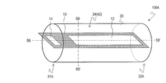
- FIG. 4 is a diagram schematically showing the electronic device 100A.
- the direction of line 5B-5B 'in FIG. 4 may be referred to as the length direction of flexible tube 20, and the direction of line 6B-6B' in FIG.
- the electronic device 100A is different from the electronic device 100 in that the sealed space 24 in the flexible tube 20 is filled with an inert gas 42.
- the electronic device 100A may be the same as the electronic device 100 except that the sealed space 24 is filled with an inert gas 42. Since the electronic device 100 ⁇ / b> A does not have a seal structure at the end along the length direction of the flexible tube 20, the entry of external moisture and oxygen into the sealed space 24 is suppressed.
- the electronic device 100A is excellent in reliability because the performance of the electronic element is suppressed from being deteriorated.
- the inert gas 42 is, for example, nitrogen or a rare gas (for example, argon, helium, or neon).
- inert means low reactivity (physically and chemically stable).
- the sealed space 24 of the electronic device 100A may be filled with an inert liquid having an insulating property (for example, liquid perfluorocarbon) instead of the inert gas 42.
- the electronic device 100A has, for example, a cylindrical shape because the sealed space 24 is filled with the inert gas 42. Since the electronic device 100A has a cylindrical shape and good appearance, the electronic device 100A can be suitably used as an electronic device (for example, a display device) used as an interior.
- One side of the flexible substrate 10 of the electronic device 100A is disposed substantially parallel to the length direction of the flexible tube 20, for example, as shown in FIGS.
- the flexible substrate 10 of the electronic device 100 ⁇ / b> A may be arranged in a spiral shape along the inner side of the flexible tube 20.
- the electronic device 100A is excellent in bending resistance.
- 5 and 6 are schematic cross-sectional views of the electronic device 100A.
- 5 is a schematic cross-sectional view taken along the line 5B-5B 'in FIG. 4
- FIG. 6 is a schematic cross-sectional view taken along the line 6B-6B' in FIG.
- the flexible tube 20 constitutes a first seal structure 31A or a second seal structure 32A at each of both ends thereof.
- 1st seal structure 31A contains the end surface 21 of the flexible tube 20, and the connection part 34 and the cover part 44 as a sealing part.
- the lid portion 44 has, for example, the same laminated structure as that of the flexible tube 20.
- the lid portion 44 may be formed from a material different from that of the flexible tube 20.
- the lid portion 44 has, for example, a shape and a size that can cover the end surface 21 of the flexible tube 20.
- the lid portion 44 is a substantially circle having a diameter that is approximately the same length as the diameter of the cylinder.
- the lid 44 has a slit 45 that matches the cross-sectional shape and size of the flexible substrate 10.
- the flexible substrate 10 passes through the slit 45 and protrudes from the first seal structure 31A.
- the connecting portion 34 is provided between the lid portion 44 and the flexible tube 20 and between the slit 45 and the flexible substrate 10.
- the first seal structure 31A may further have a welding surface as a sealing portion.
- the sealing portion of the first seal structure 31A is limited to the connection portion 34 and the lid portion 44 (or the connection portion 34, the lid portion 44 and the welding surface) as long as it has a property of closing the end of the flexible tube 20. Absent.
- the second seal structure 32A includes the end face 22 of the flexible tube 20, and a connection part 34 and a lid part 46 as a sealing part.
- the lid 46 of the second seal structure 32A may be formed from the same material as the lid 44 of the first seal structure 31A, or may be formed from a different material. Since the flexible substrate 10 does not protrude from the second seal structure 32A, the lid 46 of the second seal structure 32A does not have a slit.
- the second seal structure 32A may be the same as the first seal structure 31A except that the lid portion 46 does not have a slit.
- the electronic device 100A can change the shape of the flexible substrate 10 without changing the shape of the electronic device 100A because the sealed space 24 is filled with the inert gas 42.
- the flexible substrate 10 may be a flat surface, or as illustrated in FIG. 6B, the flexible substrate 10 may be a curved surface along the shape of the flexible tube 20. Good.
- the electronic device 100A has, for example, a string shape.
- the electronic device 100A is, for example, a substantially cylinder that extends in the length direction of the flexible tube 20.
- the diameter of the cylindrical electronic device 100A is, for example, 10 mm to 20 mm, and the length of the electronic device 100A is, for example, 450 mm.
- the width of the electronic device 100A is, for example, the diameter of the cylinder.
- the seal structure length of the electronic device 100A is the circumference of the cylinder. 2 times (2 ⁇ D).
- the seal structure length of an electronic device produced by a conventional manufacturing method having the same size is twice the circumference of the cylinder plus two times the length of the electronic device (2 ⁇ D + 20D). Since the electronic device 100A has a shorter seal structure length than an electronic device manufactured by a conventional manufacturing method, it has less moisture and / or oxygen that enter the sealed space 24 and is excellent in reliability.
- the seal structure length of the electronic device 100A is ⁇ / ((1) when the seal structure of the electronic device manufactured by the conventional manufacturing method is 1. ⁇ + x).
- the aspect ratio between the length and width of the electronic device 100A is increased, the reliability of the electronic device 100A can be improved more effectively.
- the electronic device 100A is not limited to a string shape.
- the aspect ratio between the length and the width of the electronic device 100A may be less than 10.
- the cover part 44 and the cover part 46 are prepared.
- the flexible tube 20 for example, a flexible tube having an arbitrary length may be prepared and cut to a required length.
- the diameter of the flexible tube is, for example, 10 mm to 20 mm.
- the diameter of the flexible tube is, for example, the same as the length of the diameter of the electronic device 100A that is a cylinder.
- the lid portion 44 and the lid portion 46 are formed from the same material as the flexible tube 20, the lid portion 44 and the lid portion 46 can be prepared by cutting out from the material of the flexible tube 20.
- the lid portion 44 is provided with a slit 45 that matches the cross section of the flexible substrate 10.
- an adhesive is applied between the flexible tube 20 and the lid portion 44 and between the flexible tube 20 and the lid portion 46 to adhere to each other. The applied adhesive becomes the connection portion 34.
- the flexible substrate 10 is inserted into the flexible tube 20 from the slit 45 of the lid portion 44 of the first seal structure 31A in an inert gas atmosphere or in vacuum.
- the inert gas 42 is filled in the flexible tube 20 in an inert gas atmosphere or in a vacuum.
- FIG. 7 is a diagram schematically showing the electronic device 100B.
- the direction of the 8B-8B ′ line in FIG. 7 is the length direction of the first flexible tube 20A or the second flexible tube 20B
- the direction of the 9B-9B ′ line in FIG. 7 is the first flexible tube 20A or the second flexible tube 20A. It may be referred to as the width direction of the flexible tube 20B.
- the electronic device 100B is different from the electronic device 100A in that the electronic device 100B includes the first flexible tube 20A and the second flexible tube 20B instead of the flexible tube 20.
- the electronic device 100B may be the same as the electronic device 100A except that it has two flexible tubes.
- the water vapor permeability of the first flexible tube 20A is less than 10 ⁇ 3 g / (m 2 ⁇ 24 h), and the oxygen permeability is less than 10 ⁇ 2 ml / (m 2 ⁇ 24 h ⁇ MPa).
- the water vapor permeability of the second flexible tube 20B is less than 10 ⁇ 3 g / (m 2 ⁇ 24 h), and the oxygen permeability is less than 10 ⁇ 2 ml / (m 2 ⁇ 24 h ⁇ MPa).
- the second flexible tube 20B is provided inside the first flexible tube 20A.
- the first flexible tube 20A and the second flexible tube 20B constitute a first seal structure 31B and a second seal structure 32B at both ends.
- the first flexible tube 20A has a sealed space 24 between the second flexible tube 20B.
- the electronic device 100B does not have a seal structure at the ends along the length direction of the first flexible tube 20A and the second flexible tube 20B, external moisture and oxygen may enter the sealed space 24. It is suppressed.
- the electronic device 100B is excellent in reliability because the performance of the electronic element is suppressed from being deteriorated.
- FIG. 8 and 9 are schematic cross-sectional views of the electronic device 100B.
- 8 is a schematic cross-sectional view taken along the line 8B-8B 'in FIG. 7
- FIG. 9 is a schematic cross-sectional view taken along the line 9B-9B' in FIG.
- the first flexible tube 20A may be the same as the flexible tube 20 of the electronic device 100A.
- the second flexible tube 20 ⁇ / b> B has a tube base 26, a gas barrier layer 27 outside the tube base 26, and a seal layer 28 outside the gas barrier layer 27.
- the tube base material 26, the gas barrier layer 27, and the seal layer 28 of the second flexible tube 20B are formed using the same materials and methods as the tube base material 26, the gas barrier layer 27, and the seal layer 28 of the first flexible tube 20A, respectively. obtain.
- the first flexible tube 20A and the second flexible tube 20B have substantially the same length.
- the space between the first flexible tube 20A and the second flexible tube 20B has both end faces 21 and 22 at both ends in the length direction.
- the space between the first flexible tube 20A and the second flexible tube 20B constitutes the first seal structure 31B or the second seal structure 32B at each of both ends.
- a sealed space 24 is formed therebetween. That is, the sealed space 24 is defined by the inner surface of the first flexible tube 20A, the outer surface of the second flexible tube 20B, the inner surface of the first seal structure 31B, and the inner surface of the second seal structure 32B.
- the first seal structure 31B and the second seal structure 32B do not close both ends of the second flexible tube 20B, for example.
- the inside of the second flexible tube 20B is in contact with the outside air.
- the flexible substrate 10 is, for example, a curved surface that follows the shape of the first flexible tube 20A or the second flexible tube 20B.
- the electronic device 100B can be formed into a rod shape by passing, for example, a rod-shaped metal or plastic inside the second flexible tube 20B.
- the shape of the electronic device 100B can be freely changed by passing a foldable wire (for example, a wire) through the inside of the second flexible tube 20B.
- the electronic device 100B has, for example, a string shape.
- the cross section perpendicular to the length direction of the first flexible tube 20A or the second flexible tube 20B of the electronic device 100B includes, for example, a double circle.
- the outer circle of the double circle is a cross section of the first flexible tube 20A
- the inner circle is a cross section of the second flexible tube 20B.
- the width of the electronic device 100B is, for example, the diameter of the outer circle.
- the diameter of the outer circle is, for example, 10 mm to 20 mm.
- the difference between the diameter of the outer circle and the diameter of the inner circle is, for example, 0.4 mm to 1.0 mm.
- the difference between the diameter of the outer circle and the diameter of the inner circle is, for example, 0.01 to 0.2.
- the diameter of the outer circle is 11 mm, for example, and the diameter of the inner circle is 10 mm, for example.
- the length of the electronic device 100B is, for example, 450 mm.
- the seal structure length of the electronic device 100B is , Twice the sum of the circumference of the outer circle and the circumference of the inner circle (2 ⁇ (D + d)).
- the length of the seal structure of an electronic device manufactured by a conventional manufacturing method having the same size is twice the sum of the circumference of the outer circle and the circumference of the inner circle plus four times the length of the electronic device. Length (2 ⁇ (D + d) + 40D). Since the electronic device 100B according to the embodiment of the present invention has a shorter seal structure length than an electronic device manufactured by a conventional manufacturing method, the moisture and / or oxygen that penetrates into the sealed space 24 is less and reliable. Excellent in properties.
- the seal structure length of the electronic device 100B is ( ⁇ (D + d)) where the seal structure length of the electronic device manufactured by the conventional manufacturing method is 1. ) / ( ⁇ (D + d) + 2Dx). Since d is larger than 0 and smaller than D, the seal structure length of the electronic device 100B with respect to the seal structure length of the electronic device manufactured by the conventional manufacturing method is larger than ⁇ / ( ⁇ + 2x) and smaller than ⁇ / ( ⁇ + x). When the aspect ratio between the length and width of the electronic device 100B is increased, the reliability of the electronic device 100B can be more effectively improved.
- the electronic device 100B is not limited to a string shape.
- the aspect ratio between the length and the width of the electronic device 100B may be less than 10.
- the first flexible tube 20A and the second flexible tube 20B are prepared.
- a flexible tube having an arbitrary length may be prepared and cut to a required length.
- the second flexible tube 20B is inserted inside the first flexible tube 20A in an inert atmosphere or in a vacuum.
- the first flexible tube 20A, the second flexible tube 20B, the lid portion 44, and the lid portion 46 are bonded to each other by applying an adhesive.
- the applied adhesive becomes the connection portion 34.
- the subsequent process of manufacturing the electronic device 100B is substantially the same as the manufacturing method of the electronic device 100A.
- the sealed space 24 of the electronic device 100B is filled with the inert gas 42, but the electronic device according to the embodiment of the present invention is not limited thereto.
- the sealed space 24 of the electronic device 100B may have neither gas nor liquid.
- the length of the seal structure of each of the electronic device 100, the electronic device 100A, and the electronic device 100B in which the aspect ratio between the length and the width is x is the seal structure of the electronic device manufactured by the conventional manufacturing method.
- the values are larger than 1 / (1 + x), ⁇ / ( ⁇ + x), and ⁇ / ( ⁇ + 2x) and smaller than ⁇ / ( ⁇ + x), respectively.
- the aspect ratio of the length and the width is the same, the electronic device 100 is most advantageous in that the seal structure length can be shortened as compared with the electronic device manufactured by the conventional manufacturing method, and then the electronic device. 100B is excellent.
- the reliability of the flexible electronic device can be improved.
- the flexible electronic device by embodiment of this invention is used as various electronic devices, such as a flexible display or a flexible sensor, for example.
Landscapes
- Physics & Mathematics (AREA)
- Optics & Photonics (AREA)
- Electromagnetism (AREA)
- Electroluminescent Light Sources (AREA)
Abstract
L'invention concerne un dispositif électronique (100) comprenant : un substrat flexible (10) ; une section dispositif (12) qui est supportée par le substrat flexible (10) ; une section circuit de pilotage (14) ; et un tube flexible (20) qui a une perméabilité à l'eau inférieure à 10-3 g/(m2∙24h) et une perméabilité à l'oxygène inférieure à 10-2 ml/(m2∙24 h∙MPa). Une première structure joint (31) et une deuxième structure joint (32) sont configurées sur les deux extrémités du tube flexible (20) et ledit tube flexible (20) comprend un espace scellé (24) dans son intérieur. Une partie du substrat flexible (10) et de la section dispositif (12) sont dans l'espace scellé (24) et les parties du substrat flexible (10) autres que ladite partie sont à l'extérieur de l'espace scellé (24).
Priority Applications (1)
| Application Number | Priority Date | Filing Date | Title |
|---|---|---|---|
| US15/129,045 US10193101B2 (en) | 2014-03-26 | 2015-03-24 | Electronic device |
Applications Claiming Priority (2)
| Application Number | Priority Date | Filing Date | Title |
|---|---|---|---|
| JP2014063435 | 2014-03-26 | ||
| JP2014-063435 | 2014-03-26 |
Publications (1)
| Publication Number | Publication Date |
|---|---|
| WO2015146975A1 true WO2015146975A1 (fr) | 2015-10-01 |
Family
ID=54195487
Family Applications (1)
| Application Number | Title | Priority Date | Filing Date |
|---|---|---|---|
| PCT/JP2015/058904 Ceased WO2015146975A1 (fr) | 2014-03-26 | 2015-03-24 | Dispositif électronique |
Country Status (2)
| Country | Link |
|---|---|
| US (1) | US10193101B2 (fr) |
| WO (1) | WO2015146975A1 (fr) |
Families Citing this family (3)
| Publication number | Priority date | Publication date | Assignee | Title |
|---|---|---|---|---|
| CN107924244B (zh) * | 2015-09-15 | 2021-06-15 | 株式会社村田制作所 | 操作检测装置 |
| CN111312027A (zh) * | 2018-12-11 | 2020-06-19 | 北京纳米能源与系统研究所 | 基于聚乳酸压电薄膜的微型马达、驱动器和盲文显示器 |
| DE102020200053A1 (de) * | 2020-01-06 | 2021-07-08 | Heliatek Gmbh | Verkapselungssystem für ein optoelektronisches Bauelement mit mindestens einer ersten Verkapselung und einer zweiten Verkapselung, optoelektronisches Bauelement mit einem solchen Verkapselungssystem |
Citations (6)
| Publication number | Priority date | Publication date | Assignee | Title |
|---|---|---|---|---|
| JPH05283162A (ja) * | 1992-03-31 | 1993-10-29 | Iwasaki Electric Co Ltd | エレクトロルミネッセンス素子 |
| JP2001118674A (ja) * | 1999-10-19 | 2001-04-27 | Auto Network Gijutsu Kenkyusho:Kk | 有機el表示装置 |
| JP2008293680A (ja) * | 2007-05-22 | 2008-12-04 | Konica Minolta Holdings Inc | 有機エレクトロルミネッセンス素子及びその製造方法 |
| JP2011509645A (ja) * | 2007-12-20 | 2011-03-24 | ゼネラル・エレクトリック・カンパニイ | 非接触電力およびデータ伝送システムならびに方法 |
| JP2011108564A (ja) * | 2009-11-20 | 2011-06-02 | Seiko Epson Corp | 電気光学装置、電気光学装置の製造方法ならびに電子機器 |
| WO2013094407A1 (fr) * | 2011-12-21 | 2013-06-27 | 日東電工株式会社 | Procédé de fabrication d'un élément électroluminescent organique à émission vers le haut |
Family Cites Families (13)
| Publication number | Priority date | Publication date | Assignee | Title |
|---|---|---|---|---|
| JP2002249313A (ja) | 2000-12-19 | 2002-09-06 | Toray Ind Inc | ゼオライト結晶のコーティング方法、ゼオライト結晶がコーティングされた基材、ゼオライト膜の製造方法、ゼオライト膜、および分離方法 |
| JP4945860B2 (ja) | 2001-07-24 | 2012-06-06 | 凸版印刷株式会社 | バリア性チューブ状容器 |
| JP2006299145A (ja) | 2005-04-22 | 2006-11-02 | Konica Minolta Holdings Inc | ガスバリア性フィルム、ガスバリア性フィルムを用いた有機エレクトロルミネッセンス用樹脂基材および有機エレクトロルミネッセンス素子 |
| WO2007144995A1 (fr) * | 2006-06-15 | 2007-12-21 | Sharp Kabushiki Kaisha | Affichage et son procédé de production |
| KR100824902B1 (ko) * | 2006-12-13 | 2008-04-23 | 삼성에스디아이 주식회사 | 유기 전계 발광 표시 장치 및 그 제조 방법 |
| WO2009072226A1 (fr) * | 2007-12-06 | 2009-06-11 | Sharp Kabushiki Kaisha | Dispositif d'affichage souple |
| DE102008062130A1 (de) * | 2008-12-16 | 2010-06-17 | Tesa Se | Verfahren zur Kapselung einer elektronischen Anordnung |
| WO2011155117A1 (fr) * | 2010-06-09 | 2011-12-15 | シャープ株式会社 | Dispositif d'affichage |
| WO2012002272A1 (fr) * | 2010-06-29 | 2012-01-05 | シャープ株式会社 | Dispositif d'affichage flexible et procédé de fabrication de dispositif d'affichage flexible |
| CN103339715B (zh) | 2010-12-03 | 2016-01-13 | 株式会社半导体能源研究所 | 氧化物半导体膜以及半导体装置 |
| KR102079188B1 (ko) * | 2012-05-09 | 2020-02-19 | 가부시키가이샤 한도오따이 에네루기 켄큐쇼 | 발광 장치 및 전자 기기 |
| KR102167315B1 (ko) * | 2014-04-30 | 2020-10-20 | 삼성디스플레이 주식회사 | 유기전계발광 표시장치 |
| WO2016033703A1 (fr) * | 2014-09-02 | 2016-03-10 | 深圳市柔宇科技有限公司 | Module d'affichage et dispositif électronique en étant équipé |
-
2015
- 2015-03-24 WO PCT/JP2015/058904 patent/WO2015146975A1/fr not_active Ceased
- 2015-03-24 US US15/129,045 patent/US10193101B2/en active Active
Patent Citations (6)
| Publication number | Priority date | Publication date | Assignee | Title |
|---|---|---|---|---|
| JPH05283162A (ja) * | 1992-03-31 | 1993-10-29 | Iwasaki Electric Co Ltd | エレクトロルミネッセンス素子 |
| JP2001118674A (ja) * | 1999-10-19 | 2001-04-27 | Auto Network Gijutsu Kenkyusho:Kk | 有機el表示装置 |
| JP2008293680A (ja) * | 2007-05-22 | 2008-12-04 | Konica Minolta Holdings Inc | 有機エレクトロルミネッセンス素子及びその製造方法 |
| JP2011509645A (ja) * | 2007-12-20 | 2011-03-24 | ゼネラル・エレクトリック・カンパニイ | 非接触電力およびデータ伝送システムならびに方法 |
| JP2011108564A (ja) * | 2009-11-20 | 2011-06-02 | Seiko Epson Corp | 電気光学装置、電気光学装置の製造方法ならびに電子機器 |
| WO2013094407A1 (fr) * | 2011-12-21 | 2013-06-27 | 日東電工株式会社 | Procédé de fabrication d'un élément électroluminescent organique à émission vers le haut |
Also Published As
| Publication number | Publication date |
|---|---|
| US20170110680A1 (en) | 2017-04-20 |
| US10193101B2 (en) | 2019-01-29 |
Similar Documents
| Publication | Publication Date | Title |
|---|---|---|
| US11107840B2 (en) | Method for fabricating a semiconductor device comprising an oxide semiconductor | |
| US9623633B2 (en) | Flexible display and method for manufacturing the same | |
| US8436342B2 (en) | Organic light emitting display device and method of manufacturing the same | |
| He et al. | Oxide-based thin film transistors for flexible electronics | |
| US9461269B2 (en) | Organic light emitting display and method of fabricating the same | |
| US9806285B2 (en) | Organic light-emitting diode display and manufacturing method thereof | |
| US10217958B2 (en) | Method of manufacturing curved display device | |
| JP2022171652A (ja) | 表示装置 | |
| JP2024105377A (ja) | 半導体装置 | |
| US9184224B2 (en) | Organic light-emitting diode display and manufacturing method thereof | |
| US20160104867A1 (en) | Organic light emitting diode display panel and method of fabricating the same | |
| CN101800288A (zh) | 光传感器、光传感器装置和显示装置 | |
| US10877599B2 (en) | Touch sensing unit and display device including the same | |
| WO2015146975A1 (fr) | Dispositif électronique | |
| US20220102560A1 (en) | Thin-film transistor substrate and method of manufacturing thin-film transistor substrate | |
| CN116072734A (zh) | 薄膜晶体管以及包括薄膜晶体管的显示装置 | |
| JP6717596B2 (ja) | 半導体装置 | |
| JP2010016072A (ja) | 薄膜トランジスタ | |
| KR20250127052A (ko) | 반도체 장치 및 전자 기기 | |
| JP4214152B2 (ja) | 表示装置 | |
| CN115810670A (zh) | 薄膜晶体管、其制造方法以及包括其的显示装置 | |
| US20260090220A1 (en) | Thin film transistor substrate and display device comprising the same | |
| WO2015114870A1 (fr) | Capteur de gaz | |
| KR102949188B1 (ko) | 박막 트랜지스터 및 이를 포함하는 표시장치 | |
| US20260026236A1 (en) | Display Device |
Legal Events
| Date | Code | Title | Description |
|---|---|---|---|
| 121 | Ep: the epo has been informed by wipo that ep was designated in this application |
Ref document number: 15768667 Country of ref document: EP Kind code of ref document: A1 |
|
| NENP | Non-entry into the national phase |
Ref country code: DE |
|
| WWE | Wipo information: entry into national phase |
Ref document number: 15129045 Country of ref document: US |
|
| NENP | Non-entry into the national phase |
Ref country code: JP |
|
| 122 | Ep: pct application non-entry in european phase |
Ref document number: 15768667 Country of ref document: EP Kind code of ref document: A1 |