WO2015151684A1 - Élément électroluminescent organique et dispositif électronique - Google Patents
Élément électroluminescent organique et dispositif électronique Download PDFInfo
- Publication number
- WO2015151684A1 WO2015151684A1 PCT/JP2015/055902 JP2015055902W WO2015151684A1 WO 2015151684 A1 WO2015151684 A1 WO 2015151684A1 JP 2015055902 W JP2015055902 W JP 2015055902W WO 2015151684 A1 WO2015151684 A1 WO 2015151684A1
- Authority
- WO
- WIPO (PCT)
- Prior art keywords
- light emitting
- layer
- light
- organic
- dopant
- Prior art date
- Legal status (The legal status is an assumption and is not a legal conclusion. Google has not performed a legal analysis and makes no representation as to the accuracy of the status listed.)
- Ceased
Links
Images


Classifications
-
- H—ELECTRICITY
- H05—ELECTRIC TECHNIQUES NOT OTHERWISE PROVIDED FOR
- H05B—ELECTRIC HEATING; ELECTRIC LIGHT SOURCES NOT OTHERWISE PROVIDED FOR; CIRCUIT ARRANGEMENTS FOR ELECTRIC LIGHT SOURCES, IN GENERAL
- H05B33/00—Electroluminescent light sources
- H05B33/12—Light sources with substantially two-dimensional [2D] radiating surfaces
- H05B33/14—Light sources with substantially two-dimensional [2D] radiating surfaces characterised by the chemical or physical composition or the arrangement of the electroluminescent material, or by the simultaneous addition of the electroluminescent material in or onto the light source
-
- H—ELECTRICITY
- H10—SEMICONDUCTOR DEVICES; ELECTRIC SOLID-STATE DEVICES NOT OTHERWISE PROVIDED FOR
- H10K—ORGANIC ELECTRIC SOLID-STATE DEVICES
- H10K50/00—Organic light-emitting devices
- H10K50/10—OLEDs or polymer light-emitting diodes [PLED]
- H10K50/11—OLEDs or polymer light-emitting diodes [PLED] characterised by the electroluminescent [EL] layers
-
- H—ELECTRICITY
- H10—SEMICONDUCTOR DEVICES; ELECTRIC SOLID-STATE DEVICES NOT OTHERWISE PROVIDED FOR
- H10K—ORGANIC ELECTRIC SOLID-STATE DEVICES
- H10K50/00—Organic light-emitting devices
- H10K50/10—OLEDs or polymer light-emitting diodes [PLED]
- H10K50/11—OLEDs or polymer light-emitting diodes [PLED] characterised by the electroluminescent [EL] layers
- H10K50/125—OLEDs or polymer light-emitting diodes [PLED] characterised by the electroluminescent [EL] layers specially adapted for multicolour light emission, e.g. for emitting white light
- H10K50/13—OLEDs or polymer light-emitting diodes [PLED] characterised by the electroluminescent [EL] layers specially adapted for multicolour light emission, e.g. for emitting white light comprising stacked EL layers within one EL unit
-
- H—ELECTRICITY
- H10—SEMICONDUCTOR DEVICES; ELECTRIC SOLID-STATE DEVICES NOT OTHERWISE PROVIDED FOR
- H10K—ORGANIC ELECTRIC SOLID-STATE DEVICES
- H10K50/00—Organic light-emitting devices
- H10K50/10—OLEDs or polymer light-emitting diodes [PLED]
- H10K50/19—Tandem OLEDs
-
- H—ELECTRICITY
- H10—SEMICONDUCTOR DEVICES; ELECTRIC SOLID-STATE DEVICES NOT OTHERWISE PROVIDED FOR
- H10K—ORGANIC ELECTRIC SOLID-STATE DEVICES
- H10K59/00—Integrated devices, or assemblies of multiple devices, comprising at least one organic light-emitting element covered by group H10K50/00
- H10K59/30—Devices specially adapted for multicolour light emission
- H10K59/32—Stacked devices having two or more layers, each emitting at different wavelengths
-
- H—ELECTRICITY
- H10—SEMICONDUCTOR DEVICES; ELECTRIC SOLID-STATE DEVICES NOT OTHERWISE PROVIDED FOR
- H10K—ORGANIC ELECTRIC SOLID-STATE DEVICES
- H10K2101/00—Properties of the organic materials covered by group H10K85/00
- H10K2101/10—Triplet emission
-
- H—ELECTRICITY
- H10—SEMICONDUCTOR DEVICES; ELECTRIC SOLID-STATE DEVICES NOT OTHERWISE PROVIDED FOR
- H10K—ORGANIC ELECTRIC SOLID-STATE DEVICES
- H10K85/00—Organic materials used in the body or electrodes of devices covered by this subclass
- H10K85/30—Coordination compounds
- H10K85/341—Transition metal complexes, e.g. Ru(II)polypyridine complexes
- H10K85/342—Transition metal complexes, e.g. Ru(II)polypyridine complexes comprising iridium
-
- H—ELECTRICITY
- H10—SEMICONDUCTOR DEVICES; ELECTRIC SOLID-STATE DEVICES NOT OTHERWISE PROVIDED FOR
- H10K—ORGANIC ELECTRIC SOLID-STATE DEVICES
- H10K85/00—Organic materials used in the body or electrodes of devices covered by this subclass
- H10K85/60—Organic compounds having low molecular weight
-
- H—ELECTRICITY
- H10—SEMICONDUCTOR DEVICES; ELECTRIC SOLID-STATE DEVICES NOT OTHERWISE PROVIDED FOR
- H10K—ORGANIC ELECTRIC SOLID-STATE DEVICES
- H10K85/00—Organic materials used in the body or electrodes of devices covered by this subclass
- H10K85/60—Organic compounds having low molecular weight
- H10K85/615—Polycyclic condensed aromatic hydrocarbons, e.g. anthracene
- H10K85/626—Polycyclic condensed aromatic hydrocarbons, e.g. anthracene containing more than one polycyclic condensed aromatic rings, e.g. bis-anthracene
-
- H—ELECTRICITY
- H10—SEMICONDUCTOR DEVICES; ELECTRIC SOLID-STATE DEVICES NOT OTHERWISE PROVIDED FOR
- H10K—ORGANIC ELECTRIC SOLID-STATE DEVICES
- H10K85/00—Organic materials used in the body or electrodes of devices covered by this subclass
- H10K85/60—Organic compounds having low molecular weight
- H10K85/631—Amine compounds having at least two aryl rest on at least one amine-nitrogen atom, e.g. triphenylamine
-
- H—ELECTRICITY
- H10—SEMICONDUCTOR DEVICES; ELECTRIC SOLID-STATE DEVICES NOT OTHERWISE PROVIDED FOR
- H10K—ORGANIC ELECTRIC SOLID-STATE DEVICES
- H10K85/00—Organic materials used in the body or electrodes of devices covered by this subclass
- H10K85/60—Organic compounds having low molecular weight
- H10K85/631—Amine compounds having at least two aryl rest on at least one amine-nitrogen atom, e.g. triphenylamine
- H10K85/633—Amine compounds having at least two aryl rest on at least one amine-nitrogen atom, e.g. triphenylamine comprising polycyclic condensed aromatic hydrocarbons as substituents on the nitrogen atom
-
- H—ELECTRICITY
- H10—SEMICONDUCTOR DEVICES; ELECTRIC SOLID-STATE DEVICES NOT OTHERWISE PROVIDED FOR
- H10K—ORGANIC ELECTRIC SOLID-STATE DEVICES
- H10K85/00—Organic materials used in the body or electrodes of devices covered by this subclass
- H10K85/60—Organic compounds having low molecular weight
- H10K85/649—Aromatic compounds comprising a hetero atom
- H10K85/654—Aromatic compounds comprising a hetero atom comprising only nitrogen as heteroatom
-
- H—ELECTRICITY
- H10—SEMICONDUCTOR DEVICES; ELECTRIC SOLID-STATE DEVICES NOT OTHERWISE PROVIDED FOR
- H10K—ORGANIC ELECTRIC SOLID-STATE DEVICES
- H10K85/00—Organic materials used in the body or electrodes of devices covered by this subclass
- H10K85/60—Organic compounds having low molecular weight
- H10K85/649—Aromatic compounds comprising a hetero atom
- H10K85/657—Polycyclic condensed heteroaromatic hydrocarbons
- H10K85/6572—Polycyclic condensed heteroaromatic hydrocarbons comprising only nitrogen in the heteroaromatic polycondensed ring system, e.g. phenanthroline or carbazole
Definitions
- the present invention relates to an organic electroluminescence element and an electronic device including the organic electroluminescence element.
- An organic electroluminescence element (hereinafter also referred to as an organic EL element) has a configuration in which a light emitting layer containing a light emitting compound is sandwiched between an anode and a cathode. Then, by applying an electric field, holes injected from the anode and electrons injected from the cathode are recombined in the light emitting layer to generate excitons (excitons), and the excitons are deactivated. It is a light emitting device utilizing light emission (fluorescence / phosphorescence).
- An organic EL element is an all-solid-state element composed of an organic material film having a thickness of only a submicron between electrodes, and can emit light at a voltage of several to several tens of volts. is there. Therefore, it is expected to be used for next-generation flat displays and lighting.
- the organic EL element for example, a so-called two-wavelength type white light emitting element has been proposed in which two light emitting layers having a complementary color relationship are stacked so as to achieve white light emission.
- a two-wavelength white light-emitting element can obtain a good white color on the CIE chromaticity coordinates, but its emission spectrum is not continuous and has only two peaks that are complementary. . Therefore, it is difficult to obtain broad white light close to natural light.
- a so-called three-wavelength white light-emitting element that is, a white light-emitting element having an emission spectrum having a peak in each of the red, green, and blue wavelength regions, rather than the two-wavelength white light-emitting element as described above, is also in progress.
- the three-wavelength white light-emitting elements described in Patent Document 1 and Patent Document 2 are stacked with a plurality of light-emitting elements in series, and the light emitted from each light-emitting element is overlapped, thereby achieving high current efficiency (for a certain current density). It is described that it is possible to obtain (brightness obtained). Further, it is described that a white light emitting element can be obtained by stacking light emitting elements of different emission colors in series.
- the three-wavelength white light-emitting elements described in Patent Document 1 and Patent Document 2 described above are configured for the purpose of increasing the average color rendering index (Ra), which is the average value of the evaluation numbers R1 to R8. Yes.
- Ra average color rendering index
- the three-wavelength white light emitting element having the above-described configuration cannot cope with it. .
- the present invention provides an organic electroluminescence element capable of improving the special color rendering index R9 and an electronic device having the organic electroluminescence element.
- the organic electroluminescence device of the present invention has an anode, a cathode, and a light emitting layer sandwiched between the anode and the cathode, and the light emitting dopant has a light emitting dopant exhibiting an emission spectrum having a peak in a region having a wavelength of 580 nm or more. At least two types are included.
- the electronic device of this invention has the said organic electroluminescent element.
- the emission light of the organic electroluminescence device of the present invention by using two or more kinds of dopants having a peak at a wavelength of 580 nm or more in the emission spectrum, the emission light of the organic electroluminescence device has a wide emission spectrum distribution in a region of a wavelength of 580 nm or more.
- the special color rendering index R9 can be improved by giving the emission light of the organic electroluminescence element a broad emission spectrum in a wavelength region of 580 nm or more.
- an organic electroluminescence element having an excellent special color rendering index R9 and an electronic device having the organic electroluminescence element.
- Embodiment of organic electroluminescence device (first embodiment) 2.
- Embodiment of organic electroluminescence device (second embodiment) 3.
- Embodiment of electronic device (third embodiment)
- Embodiment of Organic Electroluminescence Element (First Embodiment)>
- organic electroluminescence element organic EL element
- FIG. 1 the structure of the organic EL element of this embodiment is shown.
- the organic EL element 10 shown in FIG. 1 includes an anode 11, a first light emitting unit 12, an intermediate connector layer 13, a second light emitting unit 14, and a cathode 15. Each of these layers is stacked on the substrate 16. Details of these components will be described later.
- the anode 11 is formed on the substrate 16, and the first light emitting unit 12 is formed on the anode 11. Further, an intermediate connector layer 13 is formed on the first light emitting unit 12, and a second light emitting unit 14 is formed on the intermediate connector layer 13. Further, a cathode 15 is formed on the second light emitting unit 14.
- the organic EL element 10 has a so-called bottom emission type configuration in which the anode 11 is configured by a transparent electrode and the cathode 15 functions as a reflective electrode, and light is extracted from the substrate 16 side.
- the first light emitting unit 12 and the second light emitting unit 14 are stacked with the intermediate connector layer 13 interposed therebetween, which is a so-called tandem type configuration.
- the first light emitting unit 12 and the second light emitting unit 14 have at least one light emitting layer containing a light emitting organic material.
- the said organic EL element 10 has what is called 4 wavelength type which has the light emission dopant of each color of blue (B), green (G), and red (R) as a luminescent organic material in these light emitting layers. It is an example of a white light emitting element.
- the first light emitting layer 12 ⁇ / b> A is illustrated as the first light emitting unit 12.
- the second light emitting unit 14 a second light emitting layer 14 ⁇ / b> A and a third light emitting layer 14 ⁇ / b> B are illustrated.
- the first light emitting unit 12 and the second light emitting unit 14 may include layers other than these light emitting layers.
- the first light emitting layer 12A included in the first light emitting unit 12 includes a first red light emitting dopant and a green light emitting dopant as the light emitting dopant.
- the second light emitting layer 14A included in the second light emitting unit 14 includes a second red light emitting dopant and a green light emitting dopant.
- the third light emitting layer 14B included in the second light emitting unit 14 has a blue light emitting dopant.
- the first red light-emitting dopant and the second red light-emitting dopant are different types of dopants, and both have a peak in a region of a wavelength of 580 nm or more in the emission spectrum. Moreover, it is preferable that the peak of the emission spectrum of a 1st red light emission dopant and a 2nd red light emission dopant differs.
- the emission spectrum said here is an emission spectrum at the time of making the element which used each light emission dopant independently light-emitted.
- the first red light emitting dopant and the second red light emitting dopant By using different kinds of dopants for the first red light emitting dopant and the second red light emitting dopant, it is possible to obtain two different kinds of emission spectrum distribution having a peak at a wavelength of 580 nm or more.
- a wide distribution can be given in the emission spectrum of the organic EL element 10 in the region of a wavelength of 580 nm or more.
- the special color rendering evaluation number R9 which shows the color rendering property of red with high chroma of the organic EL element 10 can be increased by making the emission spectrum have a wide distribution in a wavelength region of 580 nm or more.
- FIG. 2 shows an example of an emission spectrum of the organic EL element 10 having the above-described configuration.
- the emission spectrum shown in FIG. 2 is an emission spectrum at the time of making the element which used each luminescent dopant independently light-emitted.
- the total emission spectrum of the light from the organic EL element 10 is in a state where the emission spectra of the respective emission dopants are integrated.
- the emission spectrum shown in FIG. 2 is an example in which a dopant having a peak at a wavelength of 616 nm is used as the first red light emitting dopant contained in the first light emitting layer 12A, and a dopant having a peak at a wavelength of 560 nm is used as the green light emitting dopant. And it is the example which used the dopant which has a peak in wavelength 594nm as a 2nd red light emission dopant contained in 2nd light emitting layer 14A, and the dopant which has a peak in wavelength 560nm similarly to 12A of 1st light emission layers as a green light emission dopant. Furthermore, it is an example using the dopant which has a peak in wavelength 475nm as a blue light emission dopant contained in the 3rd light emitting layer 14B.
- the emission spectra of the red, green, and blue light-emitting dopants each have their own peak and spread in a predetermined range, whereby white light is emitted from the organic EL element 10. It becomes the structure taken out.
- the organic EL element 10 in particular, in a region having a wavelength of 580 nm or more, which is important for increasing the special color rendering index R9, the emission spectrum of the first red emission dopant and the emission spectrum of the second red emission dopant overlap. have.
- the special color rendering index R9 of the organic EL element 10 can be improved.
- the organic EL element 10 can improve the special color rendering index R9 indicating red color rendering with high saturation without decreasing the average color rendering index Ra.
- the organic EL element 10 four types of luminescent dopants, ie, two types of luminescent dopants having a peak at a wavelength of 580 nm or more (first red luminescent dopant and second red luminescent dopant), blue luminescent dopant, and green luminescent dopant, are included.
- first red luminescent dopant and second red luminescent dopant two types of luminescent dopants having a peak at a wavelength of 580 nm or more
- blue luminescent dopant blue luminescent dopant
- green luminescent dopant green luminescent dopant
- the ratio for which one light emission dopant accounts with respect to the whole light emission spectrum of the organic EL element 10 becomes small because the wavelength range which the light emission spectrum of a mutual light emission dopant overlaps becomes large. For this reason, even if the light emission luminance of one light emitting dopant changes due to deterioration with time or current density, it can be compensated for by light emission of another light emitting dopant, and the influence on the entire light emission spectrum of the organic EL element 10 is reduced. Therefore, a white light emitting element in which the white chromaticity hardly changes with time can be configured. In addition, a white light-emitting element in which the shape of the entire emission spectrum is less dependent on the current density can be configured.
- the first light emitting layer 12A contains a green light emitting dopant together with the first red light emitting dopant.
- the second light emitting layer 14A contains a green light emitting dopant together with the second red light emitting dopant.
- the light emitting layer containing a red light emitting dopant having a peak at a wavelength of 580 nm or more contains another light emitting dopant having a peak at a wavelength of less than 580 nm together with the red light emitting dopant.
- Red light emitting dopants tend to have low carrier transport properties. For this reason, in the light emitting layer containing a red light emitting dopant, the driving voltage tends to increase due to a decrease in carrier transportability. Thus, when the 1st red light emission dopant and 2nd red light emission dopant with low carrier transport property are included in the same light emitting layer, the carrier transport property of this whole light emitting layer falls, and an organic EL element It becomes easy to increase the driving voltage. Therefore, it is preferable to include the first red light emitting dopant and the second red light emitting dopant in different light emitting layers.
- blue light-emitting dopants and green light-emitting dopants tend to have higher carrier transport properties than red light-emitting dopants.
- green light emitting dopants tend to have high carrier transport properties. For this reason, in the light emitting layer containing a blue light emitting dopant or a green light emitting dopant, an increase in driving voltage hardly occurs.
- the light emitting layer containing a red light emitting dopant having a low carrier transport property contains a blue light emitting dopant or a green light emitting dopant together with the red light emitting dopant.
- the carrier transport property of the red light-emitting dopant can be supplemented by a high carrier transport property due to the blue light-emitting dopant and the green light-emitting dopant. That is, it is possible to suppress a decrease in carrier transport property of the light emitting layer due to the red light emitting dopant, and to suppress an increase in driving voltage of the organic EL element.
- the driving voltage of the organic EL element can be lowered by adding a green light emitting dopant together with a red light emitting dopant to the light emitting layer.
- the red luminescent dopant and the green luminescent dopant are close to each other in the HOMO level and the LUMO level, so that it is difficult to generate a trap level, and it is considered that carrier transport is performed at both levels.
- the organic EL element can be driven at a low voltage by including the red light emitting dopant and the green light emitting dopant in the same light emitting layer.
- the first red light-emitting dopant and the second red light-emitting dopant having low carrier transport properties are arranged separately in the first light-emitting layer 12A and the second light-emitting layer 14A, respectively. Yes.
- the first light emitting layer 12A includes the first red light emitting dopant having a low carrier transportability and the green light emitting dopant having a high carrier transportability, thereby reducing the carrier transportability in the first light emitting layer 12A. Can be suppressed, and an increase in driving voltage can be suppressed.
- the second light-emitting layer 14A includes the second red light-emitting dopant having a low carrier transport property and the green light-emitting dopant having a high carrier transport property so that the carrier transport property in the second light-emitting layer 14A can be improved.
- the decrease can be suppressed and the increase in driving voltage can be suppressed.
- the light emitting layer near the cathode 15 has a light emitting dopant on the short wavelength side.
- the first light emitting layer 12A of the first light emitting unit 12 includes a first red light emitting dopant having a peak at a wavelength of 616 nm
- the second light emitting layer 14A of the second light emitting unit 14 includes A second red light emitting dopant having a peak at a wavelength of 594 nm is included. Therefore, the second light emitting layer 14A on the side close to the cathode 15 contains the second red light emitting dopant having a peak on the short wavelength side.
- the organic EL element 10 is a bottom emission type in which the anode 11 is a transparent electrode and the cathode 15 is a reflective electrode.
- the light incident on the cathode 15 serving as the reflective electrode acts on the free electrons in the cathode 15 to generate a plasmon mode which is a kind of waveguide mode. 15 is confined in the vicinity of the surface.
- Such light loss is called plasmon loss, and it is generally said that there is a loss of about 30 to 40%.
- it is essential to reduce the plasmon loss in order to achieve power efficiency and light emission lifetime.
- the plasmon loss is dependent on the emission wavelength, and the longer the wavelength, the greater the plasmon loss.
- the light emitting layer formed on the reflective electrode side includes a light emitting dopant having a peak in a short wavelength region, and the light emitting layer located far from the reflective electrode includes a light emitting dopant having a peak in a long wavelength region.
- the plasmon loss of the organic EL element 10 can be suppressed.
- the cathode 15 is a reflective electrode made of metal, a second red light-emitting dopant having a peak on the short wavelength side is added to the second light-emitting layer 14A of the second light-emitting unit 14 on the side close to the cathode 15. It is preferable to include.
- the first light emitting layer 12A on the side close to the anode 11 preferably contains a first red light emitting dopant having a peak on the long wavelength side. By setting it as such a structure, the luminous efficiency of the organic EL element 10 can be improved.
- the dopant contained in the light emitting layer is similarly reversed.
- a light emitting layer having a peak in the short wavelength region is included in the light emitting layer near the electrode on the light reflecting side, and a light emitting dopant having a peak in the long wavelength region is included in the light emitting layer far from the electrode on the light reflecting side. Therefore, plasmon loss can be suppressed.
- each structure of the organic EL element demonstrated below is an example for demonstrating embodiment, and it is also possible to apply another structure suitably in the range which can comprise the above-mentioned organic EL element. .
- an electrode material made of a metal, an alloy, an electrically conductive compound, and a mixture thereof having a high work function (4 eV or more, preferably 4.3 V or more) is used.
- an electrode substance include metals such as Au and Ag, alloys thereof, and conductive transparent materials such as CuI, indium tin oxide (ITO), SnO 2 , and ZnO.
- amorphous material such as IDIXO (In 2 O 3 —ZnO) capable of forming a transparent conductive film may be used.
- the transmittance be larger than 10%.
- the sheet resistance as the anode is several hundred ⁇ / sq. The following is preferred. Further, although the thickness of the anode depends on the material, it is usually selected in the range of 10 nm to 1 ⁇ m, preferably 10 nm to 200 nm.
- the first light emitting unit 12 is provided between the anode 11 and the intermediate connector layer 13 and includes at least one light emitting layer including an organic material having light emitting properties.
- the second light emitting unit 14 includes at least one light emitting layer that is provided between the intermediate connector layer 13 and the cathode 15 and contains a light emitting organic material.
- another layer may be provided between the light emitting layer and the anode 11, the intermediate connector layer 13, and the cathode 15.
- first light emitting unit 12 and the second light emitting unit 14 will be collectively described as a light emitting unit. Further, the first to third light emitting layers formed in the first light emitting unit 12 and the second light emitting unit 14 will be described as a light emitting layer as a whole.
- Typical element configurations of the light emitting unit include the following configurations, but are not limited thereto.
- the light emitting layer is formed of a single layer or a plurality of layers.
- the electron transport layer is a layer having a function of transporting electrons.
- the electron transport layer includes an electron injection layer and a hole blocking layer in a broad sense. Further, the electron transport layer may be composed of a plurality of layers.
- the hole transport layer is a layer having a function of transporting holes.
- the hole transport layer includes a hole injection layer and an electron blocking layer in a broad sense.
- the hole transport layer may be composed of a plurality of layers.
- each layer for example, a known thin film formation such as a vacuum deposition method, a spin coating method, a casting method, an LB method (Langmuir-Blodget method), an ink jet method, a spray method, a printing method, a slot type coater method, etc.
- the film can be formed by the method.
- the phosphorescent light emitting material and the fluorescent light emitting material may be mixed in the light emitting layer in the light emitting unit, but it is preferable that the phosphorescent light emitting material or the fluorescent light emitting material is used alone.
- the fluorescent light emitting layer and the phosphorescent light emitting layer are preferably a host or dopant type light emitting layer.
- the light emission dopant contained in a light emitting layer may be contained with the uniform density
- each light emitting unit preferably has the same number of light emitting layers. Thereby, the number of materials used can be reduced, and there are advantages in production such as cost and quality control. Furthermore, the vapor deposition process has an advantage in terms of production efficiency, such as easy formation of a film forming chamber for each light emitting unit. For the above reasons, when stacking white light emitting units, it is preferable that the configuration and materials of all layers including the light emitting layer are the same.
- an organic EL element that emits white light can be obtained by providing a blue light-emitting unit and a light-emitting unit that emits a complementary green, yellow-green, yellow, or orange light-emitting color.
- the “complementary color” relationship is a relationship between colors that become achromatic when mixed. That is, white light emission can be obtained by mixing light emission of substances emitting light of complementary colors.
- a layer exhibiting green and red light-emitting colors is provided in any light-emitting unit. It is preferable.
- blue, green, and red light-emitting materials can be mixed in one light-emitting layer and provided in the light-emitting unit as a light-emitting layer that emits white light.
- the film thickness of the individual layers included in each light emitting unit is not particularly limited. It is preferable to adjust within the range of 5 to 200 nm from the viewpoint of homogeneity of the film to be formed, application of unnecessary high voltage at the time of light emission, and improvement of the stability of the emission color with respect to the drive current. More preferably, it is adjusted to a range of 10 to 100 nm or less.
- each layer which comprises a light emission unit is demonstrated.
- the light emitting layer is a layer including a light emitting organic semiconductor thin film that provides a field in which electrons and holes injected from an electrode or an adjacent layer are recombined to emit light via excitons.
- the light emitting layer preferably contains a light emitting dopant (a light emitting dopant compound, a dopant compound, also simply referred to as a dopant) and a host compound (a matrix material, a light emitting host compound, also simply referred to as a host).
- the method for forming the light emitting layer is not particularly limited, and the light emitting layer can be formed by a conventionally known method such as a vacuum deposition method or a wet method (wet process). It is preferable to form by a wet method from the manufacturing cost of an organic EL element.
- Luminescent dopant As the luminescent dopant, a fluorescent luminescent dopant (also referred to as a fluorescent dopant or a fluorescent compound) and a phosphorescent dopant (also referred to as a phosphorescent dopant or a phosphorescent compound) are preferably used.
- the concentration of the light-emitting dopant in the light-emitting layer can be arbitrarily determined based on the specific dopant used and the device requirements.
- the concentration of the optical dopant may be contained at a uniform concentration relative to the thickness direction of the light emitting layer, or may have an arbitrary concentration distribution.
- the light emitting layer may contain a plurality of types of light emitting dopants. For example, a combination of dopants having different structures, or a combination of a fluorescent luminescent dopant and a phosphorescent luminescent dopant may be used. Thereby, arbitrary luminescent colors can be obtained.
- one or more light-emitting layers contain a plurality of light-emitting dopants having different emission colors and emit white light.
- the combination of light-emitting dopants that exhibit white include a combination of blue and orange, a combination of blue, green, and red.
- the phosphorescent dopant is a compound in which light emission from an excited triplet is observed.
- the phosphorescent dopant is a compound that emits phosphorescence at room temperature (25 ° C.), and has a phosphorescence quantum yield of 0 at 25 ° C. .01 or more compounds.
- a preferable phosphorescence quantum yield is 0.1 or more.
- the phosphorescent quantum yield can be measured by the method described in Spectroscopic II, page 398 (1992 edition, Maruzen) of Experimental Chemistry Course 4 of the 4th edition.
- the phosphorescence quantum yield in a solution can be measured using various solvents.
- the phosphorescence emitting dopant used for the light emitting layer should just achieve the said phosphorescence quantum yield (0.01 or more) in any solvent.
- an excited state of the host compound is generated by recombination of carriers on the host compound to which carriers are transported. It is an energy transfer type in which light is emitted from the phosphorescent dopant by transferring this energy to the phosphorescent dopant.
- the other is a carrier trap type in which a phosphorescent dopant becomes a carrier trap, carrier recombination occurs on the phosphorescent dopant, and light emission from the phosphorescent dopant is obtained. In any case, it is a condition that the excited state energy of the phosphorescent dopant is lower than the excited state energy of the host compound.
- the phosphorescent dopant can be appropriately selected from known materials used for the light emitting layer of the organic EL element.
- Specific examples of known phosphorescent dopants include compounds described in the following documents.
- Preferred examples of the phosphorescent compound include compounds represented by general formula (4), general formula (5), and general formula (6) described in paragraphs [0185] to [0235] of JP2013-4245A. be able to.
- a preferable phosphorescent dopant is an organometallic complex having Ir as a central metal. More preferably, a complex containing at least one coordination mode of a metal-carbon bond, a metal-nitrogen bond, a metal-oxygen bond, and a metal-sulfur bond is preferable.
- the fluorescent light-emitting dopant is a compound that can emit light from an excited singlet, and is not particularly limited as long as light emission from the excited singlet is observed.
- Examples of the fluorescent light-emitting dopant include anthracene derivatives, pyrene derivatives, chrysene derivatives, fluoranthene derivatives, perylene derivatives, fluorene derivatives, arylacetylene derivatives, styrylarylene derivatives, styrylamine derivatives, arylamine derivatives, boron complexes, coumarin derivatives, Examples include pyran derivatives, cyanine derivatives, croconium derivatives, squalium derivatives, oxobenzanthracene derivatives, fluorescein derivatives, rhodamine derivatives, pyrylium derivatives, perylene derivatives, polythiophene derivatives, rare earth complex compounds, and the like.
- a light emitting dopant using delayed fluorescence may be used as the fluorescent light emitting dopant.
- Specific examples of the luminescent dopant using delayed fluorescence include compounds described in, for example, International Publication No. 2011/156793, Japanese Patent Application Laid-Open No. 2011-213643, Japanese Patent Application Laid-Open No. 2010-93181, and the like.
- the host compound is a compound mainly responsible for charge injection and transport in the light emitting layer, and its own light emission is not substantially observed in the organic EL element.
- it is a compound having a phosphorescence quantum yield of phosphorescence of less than 0.1 at room temperature (25 ° C.), more preferably a compound having a phosphorescence quantum yield of less than 0.01.
- the mass ratio in the layer is 20% or more among the compounds contained in a light emitting layer.
- the excited state energy of a host compound is higher than the excited state energy of the light emission dopant contained in the same layer.
- a host compound may be used independently or may be used in combination of multiple types. By using a plurality of types of host compounds, it is possible to adjust the movement of electric charges, and it is possible to increase the efficiency of the organic EL element.
- the compound conventionally used with an organic EL element can be used.
- it may be a low molecular compound, a high molecular compound having a repeating unit, or a compound having a reactive group such as a vinyl group or an epoxy group.
- Tg glass transition temperature
- the glass transition point (Tg) is a value determined by a method based on JIS-K-7121 using DSC (Differential Scanning Colorimetry).
- the electron transport layer used for the organic EL element is made of a material having a function of transporting electrons, and has a function of transmitting electrons injected from the cathode to the light emitting layer.
- the electron transport material may be used alone or in combination of two or more.
- the total thickness of the electron transport layer is not particularly limited, but is usually in the range of 2 nm to 5 ⁇ m, more preferably 2 nm to 500 nm, and further preferably 5 nm to 200 nm.
- the organic EL element when the light generated in the light emitting layer is extracted, the light extracted directly from the light emitting layer through the anode and the light extracted after being reflected by the cathode positioned opposite to the anode cause interference. It is known. Therefore, in the organic EL element, it is preferable to adjust the total thickness of the light-emitting unit by appropriately adjusting the total thickness of the electron transport layer between several nm to several ⁇ m. On the other hand, since the voltage when the thickness of the electron transport layer tends to increase, especially in the case a thick film thickness, the electron mobility of the electron transport layer is preferably 10 -5 cm 2 / Vs or more .
- the material used for the electron transport layer may have any of the electron injection property or the transport property or the hole barrier property. Any one can be selected and used. Examples thereof include nitrogen-containing aromatic heterocyclic derivatives, aromatic hydrocarbon ring derivatives, dibenzofuran derivatives, dibenzothiophene derivatives, silole derivatives, and the like.
- nitrogen-containing aromatic heterocyclic derivatives examples include carbazole derivatives, azacarbazole derivatives (one or more carbon atoms constituting the carbazole ring are substituted with nitrogen atoms), pyridine derivatives, pyrimidine derivatives, pyrazine derivatives, pyridazine derivatives, triazine derivatives.
- aromatic hydrocarbon ring derivative examples include naphthalene derivatives, anthracene derivatives, triphenylene and the like.
- a metal complex having a quinolinol skeleton or a dibenzoquinolinol skeleton as a ligand such as tris (8-quinolinol) aluminum (Alq3), tris (5,7-dichloro-8-quinolinol) aluminum, tris (5,7- Dibromo-8-quinolinol) aluminum, tris (2-methyl-8-quinolinol) aluminum, tris (5-methyl-8-quinolinol) aluminum, bis (8-quinolinol) zinc (Znq), etc., and metal complexes thereof
- a metal complex in which the central metal is replaced with In, Mg, Cu, Ca, Sn, Ga, or Pb can also be used as an electron transporting material.
- metal-free or metal phthalocyanine, or those having the terminal substituted with an alkyl group or a sulfonic acid group can be preferably used as the electron transporting material.
- the distyrylpyrazine derivative exemplified as the material for the light emitting layer can also be used as an electron transport material, and an inorganic semiconductor such as n-type-Si, n-type-SiC, etc. as in the case of the hole injection layer and the hole transport layer. Can also be used as an electron transporting material.
- a polymer material in which these materials are introduced into a polymer chain or these materials are used as a polymer main chain can also be used.
- a doping material may be doped into the electron transport layer as a guest material to form an electron transport layer having a high n property (electron rich).
- the doping material include metal compounds such as metal complexes and metal halides, and other n-type dopants.
- Specific examples of the electron transport layer having such a structure include, for example, JP-A-4-297076, JP-A-10-270172, JP-A-2000-196140, 2001-102175, J. Appl. Phys., 95, 5773 (2004) and the like.
- preferable electron transport materials include, but are not limited to, compounds described in the following documents.
- U.S. Pat.No. 6,528,187, U.S. Pat.No. 7,230,107 U.S. Patent Publication No. 20050025993, U.S. Pat. Publication No. 2004036077, U.S. Pat. Publication No. 200901115316, U.S. Pat. 2003060956, WO200008132085, Appl. Phys. Lett. 75, 4 (1999), Appl. Phys. Lett. 79, 449 (2001), Appl. Phys. Lett. 81, 162 (2002), Appl. Phys. Lett. 81, 162 (2002), Appl. Phys. Lett. 81, 162 (2002), Appl. Phys.
- More preferable electron transport materials include pyridine derivatives, pyrimidine derivatives, pyrazine derivatives, triazine derivatives, dibenzofuran derivatives, dibenzothiophene derivatives, carbazole derivatives, azacarbazole derivatives, and benzimidazole derivatives.
- the hole blocking layer is a layer having a function of an electron transport layer in a broad sense. Preferably, it is made of a material having a function of transporting electrons and a small ability to transport holes. By blocking holes while transporting electrons, the recombination probability of electrons and holes can be improved. Moreover, the structure of the above-mentioned electron carrying layer can be used as a hole-blocking layer as needed.
- the hole blocking layer provided in the organic EL element is preferably provided adjacent to the cathode side of the light emitting layer.
- the thickness of the hole blocking layer is preferably in the range of 3 to 100 nm, more preferably in the range of 5 to 30 nm.
- the material used for the hole blocking layer the material used for the above-described electron transport layer is preferably used, and the material used as the above-described host compound is also preferably used for the hole blocking layer.
- the electron injection layer (also referred to as “cathode buffer layer”) is a layer provided between the cathode and the light emitting layer in order to lower the driving voltage and improve the light emission luminance.
- An example of an electron injection layer can be found in the second chapter, Chapter 2, “Electrode Materials” (pages 123-166) of “Organic EL devices and their industrialization front line (issued by NTT Corporation on November 30, 1998)”. Are listed.
- the electron injection layer is provided as necessary, and is provided between the cathode and the light emitting layer or between the cathode and the electron transport layer as described above.
- the electron injection layer is preferably a very thin film, and the film thickness is preferably in the range of 0.1 nm to 5 nm, depending on the material.
- membrane in which a constituent material exists intermittently may be sufficient.
- JP-A-6-325871, JP-A-9-17574, and JP-A-10-74586 Specific examples of materials preferably used for the electron injection layer include metals typified by strontium and aluminum, alkali metal compounds typified by lithium fluoride, sodium fluoride, and potassium fluoride, magnesium fluoride, and fluoride. Examples thereof include alkaline earth metal compounds typified by calcium, metal oxides typified by aluminum oxide, metal complexes typified by lithium 8-hydroxyquinolate (Liq), and the like.
- the material used for said electron injection layer may be used independently, and may be used in combination of multiple types.
- the hole transport layer is made of a material having a function of transporting holes.
- the hole transport layer is a layer having a function of transmitting holes injected from the anode to the light emitting layer.
- the total thickness of the hole transport layer is not particularly limited, but is usually in the range of 5 nm to 5 ⁇ m, more preferably 2 nm to 500 nm, and further preferably 5 nm to 200 nm.
- the material used for the hole transport layer may have any of a hole injection property or a transport property and an electron barrier property.
- a hole transport material an arbitrary material can be selected and used from conventionally known compounds.
- the hole transport material may be used alone or in combination of two or more.
- Hole transport materials include, for example, porphyrin derivatives, phthalocyanine derivatives, oxazole derivatives, oxadiazole derivatives, triazole derivatives, imidazole derivatives, pyrazoline derivatives, pyrazolone derivatives, phenylenediamine derivatives, hydrazone derivatives, stilbene derivatives, polyarylalkane derivatives, tria Reelamine derivatives, carbazole derivatives, indolocarbazole derivatives, isoindole derivatives, acene derivatives such as anthracene and naphthalene, fluorene derivatives, fluorenone derivatives, polyvinyl carbazole, polymer materials having aromatic amine introduced in the main chain or side chain, or Oligomer, polysilane, conductive polymer or oligomer (eg, PEDOT: PSS, aniline copolymer, polyaniline, polythiophene, etc.) And the like.
- PEDOT PEDOT: PS
- triarylamine derivatives examples include a benzidine type typified by ⁇ -NPD, a starburst type typified by MTDATA, and a compound having fluorene or anthracene in the triarylamine linking core part.
- hexaazatriphenylene derivatives described in JP-T-2003-519432 and JP-A-2006-135145 can also be used as the hole transport material.
- a hole transport layer having a high p property doped with impurities can also be used.
- the configurations described in JP-A-4-297076, JP-A-2000-196140, 2001-102175, J. Appl. Phys., 95, 5773 (2004), etc. can also be applied to the transport layer.
- so-called p-type hole transport materials and p-type materials as described in JP-A-11-251067 and J. Huang et.al. (Applied Physics Letters 80 (2002), p. 139).
- Inorganic compounds such as -Si and p-type -SiC can also be used.
- ortho-metalated organometallic complexes having Ir or Pt as the central metal as typified by Ir (ppy) 3 are also preferably used.
- the hole transport material a triarylamine derivative, a carbazole derivative, an indolocarbazole derivative, an azatriphenylene derivative, an organometallic complex, or an aromatic amine is introduced into the main chain or side chain.
- the polymer materials or oligomers used are preferably used.
- Specific examples of the hole transport material include, but are not limited to, the compounds described in the following documents in addition to the documents listed above. Appl. Phys. Lett. 69, 2160 (1996), J. Lumin. 72-74, 985 (1997), Appl. Phys. Lett. 78, 673 (2001), Appl. Phys. Lett. 90, 183503 (2007) ), Appl.
- the electron blocking layer is a layer having a function of a hole transport layer in a broad sense. Preferably, it is made of a material having a function of transporting holes and a small ability to transport electrons.
- the electron blocking layer can improve the probability of recombination of electrons and holes by blocking electrons while transporting holes.
- the structure of the above-mentioned hole transport layer can be used as an electron blocking layer of an organic EL element as needed.
- the electron blocking layer provided in the organic EL element is preferably provided adjacent to the anode side of the light emitting layer.
- the thickness of the electron blocking layer is preferably in the range of 3 to 100 nm, and more preferably in the range of 5 to 30 nm.
- the materials used for the electron blocking layer can be preferably used.
- the material used as the above-mentioned host compound can also be preferably used as the electron blocking layer.
- the hole injection layer (also referred to as “anode buffer layer”) is a layer provided between the anode and the light emitting layer in order to lower the driving voltage and improve the light emission luminance.
- An example of the hole injection layer is “Organic EL device and its industrialization front line (November 30, 1998, issued by NTT)”, Chapter 2, Chapter 2, “Electrode material” (pages 123-166). It is described in.
- the hole injection layer is provided as necessary, and is provided between the anode and the light emitting layer or between the anode and the hole transport layer as described above.
- Examples of the material used for the hole injection layer include the materials used for the hole transport layer described above. Among them, phthalocyanine derivatives typified by copper phthalocyanine, hexaazatriphenylene derivatives as described in JP-T-2003-519432, JP-A-2006-135145, etc., metal oxides typified by vanadium oxide, amorphous Conductive polymers such as carbon, polyaniline (emeraldine) and polythiophene, orthometalated complexes represented by tris (2-phenylpyridine) iridium complex, and triarylamine derivatives are preferred.
- the materials used for the hole injection layer described above may be used alone or in combination of two or more.
- the intermediate connector layer 13 may have a structure in which a metal single layer is formed to a thickness of about 0.1 to 10 nm.
- the charge generation layer may have a function of injecting electrons into the first light emitting unit 12 and a function of injecting holes into the second light emitting unit 14.
- plasmon loss may occur.
- the intermediate connector layer 13 it is preferable to use a structure of a charge generation layer in which a layer having a function of injecting holes and a layer having a function of injecting electrons are stacked without including a metal single layer. .
- the intermediate connector layer 13 can be formed using the same material as the anode and the cathode.
- the intermediate connector layer 13 can be formed using a material having lower conductivity than the anode and the cathode.
- an insulator or a semiconductor such as lithium oxide, lithium fluoride, cesium carbonate, or the like can be used.
- a material in which an electron donating substance is added to a substance having a high electron transporting property can be used.
- Examples of the substance having a high electron transporting property include tris (8-quinolinolato) aluminum (abbreviation: Alq3), tris (4-methyl-8-quinolinolato) aluminum (abbreviation: Almq3), and bis (10-hydroxybenzo [h].
- a metal complex having a quinoline skeleton or a benzoquinoline skeleton such as quinolinato) beryllium (abbreviation: BeBq2), bis (2-methyl-8-quinolinolato) (4-phenylphenolato) aluminum (abbreviation: BAlq) can be used. .
- bis [2- (2-hydroxyphenyl) benzoxazolate] zinc (abbreviation: Zn (BOX) 2)
- bis [2- (2-hydroxyphenyl) benzothiazolate] zinc (abbreviation: Zn ( Metal complexes having oxazole and thiazole ligands such as BTZ) 2)
- Zn Metal complexes having oxazole and thiazole ligands such as BTZ
- 2- (4-biphenylyl) -5- (4-tert-butylphenyl) -1,3,4-oxadiazole (abbreviation: PBD), 1,3-bis [5- (P-tert-butylphenyl) -1,3,4-oxadiazol-2-yl] benzene (abbreviation: OXD-7), 3- (4-biphenylyl) -4-phenyl-5- (4-tert -Butylphenyl) -1,2,4-triazole (abbreviation: TAZ), bathophenanthroline (abbreviation: BPhen), bathocuproine (abbreviation: BCP), and the like can also be used.
- PBD 4,4-biphenylyl) -5- (4-tert-butylphenyl) -1,3,4-oxadiazole
- OXD-7 1,3-bis [5- (P-tert-butylphenyl) -1,3,4-
- the substance having a high electron transporting property mainly has an electron mobility of 10 ⁇ 6 cm 2 / Vs or more. Note that other than the above substances, any substance that has a property of transporting more electrons than holes can be used.
- the electron injecting property can be increased by adding an electron donating substance to a substance having a high electron transporting property. For this reason, the drive voltage of a light emitting element can be reduced.
- an alkali metal an alkaline earth metal, a rare earth metal, a metal belonging to Group 13 of the periodic table, an oxide thereof, or a carbonate thereof can be used.
- lithium (Li), cesium (Cs), magnesium (Mg), calcium (Ca), ytterbium (Yb), indium (In), lithium oxide, cesium carbonate, or the like is preferably used.
- an organic compound such as tetrathianaphthacene may be used as a donor substance.
- the layer having a function of injecting holes in the intermediate connector layer 13 for example, a semiconductor such as molybdenum oxide, vanadium oxide, rhenium oxide, ruthenium oxide, or an insulator can be used.
- a material in which an electron-accepting substance is added to a substance having a high hole-transport property can be used.
- a layer made of an electron accepting substance may be used.
- Examples of the substance having a high hole-transport property include 4,4′-bis [N- (1-naphthyl) -N-phenylamino] biphenyl (abbreviation: NPB or ⁇ -NPD), N, N′-bis ( 3-methylphenyl) -N, N′-diphenyl- [1,1′-biphenyl] -4,4′-diamine (abbreviation: TPD), 4,4 ′, 4 ′′ -tris (N, N-diphenyl) Aromatic amine compounds such as amino) triphenylamine (abbreviation: TDATA), 4,4 ′, 4 ′′ -tris [N- (3-methylphenyl) -N-phenylamino] triphenylamine (abbreviation: MTDATA) Etc. can be used.
- NPB or ⁇ -NPD N, N′-bis ( 3-methylphenyl) -N, N′-diphenyl- [1,1′-b
- the above-described substance having a high hole-transport property is mainly a substance having a hole mobility of 10 ⁇ 6 cm 2 / Vs or higher. Note that other than the above substances, any substance that has a property of transporting more holes than electrons may be used. Further, the above host material may be used.
- the hole-injecting property can be increased by adding an electron-accepting substance to a substance having a high hole-transporting property. For this reason, the drive voltage of a light emitting element can be reduced.
- the electron-accepting substance 7,7,8,8-tetracyano-2,3,5,6-tetrafluoroquinodimethane (abbreviation: F4-TCNQ), chloranil, or the like can be used. Transition metal oxides can also be used. Alternatively, an oxide of a metal belonging to Groups 4 to 8 in the periodic table can be used.
- vanadium oxide, niobium oxide, tantalum oxide, chromium oxide, molybdenum oxide, tungsten oxide, manganese oxide, and rhenium oxide are preferable because of their high electron accepting properties.
- molybdenum oxide is especially preferable because it is stable in the air, has a low hygroscopic property, and is easy to handle.
- another layer may be introduced between the layer having a function of injecting holes and the layer having a function of injecting electrons, if necessary.
- a conductive layer such as ITO or an electronic relay layer may be provided.
- the electron relay layer has a function of reducing voltage loss generated between a layer having a function of injecting holes and a layer having a function of injecting electrons.
- a material having an LUMO level of approximately ⁇ 5.0 eV or more is preferably used, and a material having ⁇ 5.0 eV or more and ⁇ 3.0 eV or less is more preferably used.
- PTCDA 3,4,9,10-perylenetetracarboxylic dianhydride
- PTCBI 3,4,9,10-perylenetetracarboxylic bisbenzimidazole
- an electrode material made of a metal having a small work function (4 eV or less) (referred to as an electron injecting metal), an alloy, an electrically conductive compound, and a mixture thereof is used.
- an electron injecting metal referred to as an electron injecting metal
- Specific examples of such electrode materials include sodium, sodium-potassium alloy, magnesium, lithium, magnesium / copper mixture, magnesium / silver mixture, magnesium / aluminum mixture, magnesium / indium mixture, aluminum / aluminum oxide (Al 2 O 3 ) Mixtures, indium, lithium / aluminum mixtures, aluminum, silver, silver-based alloys, aluminum / silver mixtures, rare earth metals, and the like.
- the cathode 15 can be produced by using the above electrode material by a method such as vapor deposition or sputtering.
- the sheet resistance of the cathode 15 is several hundred ⁇ / sq. The following is preferred.
- the thickness of the cathode 15 is usually selected in the range of 10 nm to 5 ⁇ m, preferably 50 nm to 200 nm.
- the substrate 16 used in the organic EL element 10 is not particularly limited in the type such as glass and plastic, and preferably glass, quartz, and a transparent resin film can be used. Particularly preferred is a resin film that can give flexibility to the organic EL element 10.
- polyesters such as polyethylene terephthalate (PET) and polyethylene naphthalate (PEN), polyethylene, polypropylene, cellophane, cellulose diacetate, cellulose triacetate (TAC), cellulose acetate butyrate, cellulose acetate propionate ( CAP), cellulose esters such as cellulose acetate phthalate, cellulose nitrate or derivatives thereof, polyvinylidene chloride, polyvinyl alcohol, polyethylene vinyl alcohol, syndiotactic polystyrene, polycarbonate, norbornene resin, polymethylpentene, polyether ketone, polyimide , Polyethersulfone (PES), polyphenylene sulfide, polysulfone , Polyetherimide, polyetherketoneimide, polyamide, fluororesin, nylon, polymethylmethacrylate, acrylic or polyarylates, cyclone resins such as Arton (trade name, manufactured by JSR) or Appel (trade name
- a barrier film made of an inorganic film, an organic film, or a hybrid film of both may be formed on the surface of the resin film.
- the barrier film had a water vapor transmission rate (25 ⁇ 0.5 ° C., relative humidity (90 ⁇ 2)% RH) of 0.01 g / (m 2 ⁇ 24 h) measured by a method according to JIS K 7129-1992.
- the following barrier films are preferred.
- the oxygen permeability measured by a method according to JIS K 7126-1987 is 10 ⁇ 3 ml / (m 2 ⁇ 24 h ⁇ atm) or less, and the water vapor permeability is 10 ⁇ 5 g / (m 2 ⁇ 24h)
- the following high-barrier film is preferable.
- the material for forming the barrier film may be any material that has a function of suppressing intrusion of elements that cause deterioration of elements such as moisture and oxygen.
- silicon oxide, silicon dioxide, silicon nitride, or the like can be used.
- the method for forming the barrier film is not particularly limited.
- the vacuum deposition method, sputtering method, reactive sputtering method, molecular beam epitaxy method, cluster ion beam method, ion plating method, plasma polymerization method, atmospheric pressure plasma weight A combination method, a plasma CVD method, a laser CVD method, a thermal CVD method, a coating method, or the like can be used.
- an atmospheric pressure plasma polymerization method as described in JP-A-2004-68143 is preferable.
- sealing means used for sealing the organic EL element 10 include a method of bonding a sealing member, an electrode, and a support substrate with an adhesive.
- a sealing member it should just be arrange
- transparency and electrical insulation are not particularly limited.
- Specific examples include a glass plate, a polymer plate, a polymer film, a metal plate / film, and the like.
- the glass plate include soda-lime glass, barium / strontium-containing glass, lead glass, aluminosilicate glass, borosilicate glass, barium borosilicate glass, and quartz.
- the polymer plate and polymer film include polycarbonate, acrylic, polyethylene terephthalate, polyether sulfide, and polysulfone.
- the metal plate include metals including one or more selected from the group consisting of stainless steel, iron, copper, aluminum, magnesium, nickel, zinc, chromium, titanium, molybdenum, silicon, germanium, and tantalum, and alloys.
- the organic EL element 10 can be thinned, a polymer film or a metal film can be preferably used. Further, the polymer film preferably has an oxygen permeability of 10 ⁇ 3 g / (m 2 ⁇ 24 h) or less and a water vapor permeability of 10 ⁇ 3 g / (m 2 ⁇ 24 h) or less. Further, it is more preferable that both the water vapor permeability and the oxygen permeability are 10 ⁇ 5 g / (m 2 ⁇ 24 h) or less.
- adhesives include photo-curing and thermosetting adhesives having reactive vinyl groups such as acrylic acid oligomers and methacrylic acid oligomers, and moisture curing adhesives such as 2-cyanoacrylates.
- photo-curing and thermosetting adhesives having reactive vinyl groups such as acrylic acid oligomers and methacrylic acid oligomers, and moisture curing adhesives such as 2-cyanoacrylates.
- fever and chemical curing types such as an epoxy type
- hot-melt type polyamide, polyester, and polyolefin can be mentioned.
- a cationic curing type ultraviolet curing epoxy resin adhesive can be mentioned.
- an organic EL element may deteriorate with heat processing, it is preferable that it can carry out adhesive hardening from room temperature to 80 degreeC. Further, a desiccant may be dispersed in the adhesive. Application
- coating of the adhesive agent to a sealing part may use commercially available dispenser, and may print it like screen printing.
- an inert gas such as nitrogen or argon, or an inert liquid such as fluorinated hydrocarbon or silicon oil is injected in the gas phase and the liquid phase.
- a vacuum can also be used.
- a hygroscopic compound can also be enclosed inside.
- hygroscopic compound examples include metal oxides (for example, sodium oxide, potassium oxide, calcium oxide, barium oxide, magnesium oxide, aluminum oxide) and sulfates (for example, sodium sulfate, calcium sulfate, magnesium sulfate, cobalt sulfate).
- metal oxides for example, sodium oxide, potassium oxide, calcium oxide, barium oxide, magnesium oxide, aluminum oxide
- sulfates for example, sodium sulfate, calcium sulfate, magnesium sulfate, cobalt sulfate.
- metal halides eg calcium chloride, magnesium chloride, cesium fluoride, tantalum fluoride, cerium bromide, magnesium bromide, barium iodide, magnesium iodide etc.
- perchloric acids eg perchloric acid Barium, magnesium perchlorate, and the like
- anhydrous salts are preferably used in sulfates, metal halides, and perchloric acids.
- a protective film or a protective plate may be provided outside the sealing film.
- the mechanical strength is not necessarily high, and thus it is preferable to provide such a protective film and a protective plate.
- the same glass plate, polymer plate / film, metal plate / film, etc. as those used for the sealing can be used, but the polymer film is light and thin. Is preferably used.
- An organic EL element emits light inside a layer having a higher refractive index than air (within a refractive index of about 1.6 to 2.1), and only about 15 to 20% of the light generated in the light emitting layer is emitted. It is generally said that it cannot be taken out. This is because the light incident on the interface (interface between the transparent substrate and air) at an angle ⁇ greater than the critical angle causes total reflection and cannot be taken out of the element, or between the transparent electrode or light emitting layer and the transparent substrate. This is because the light undergoes total reflection between them, and the light is guided through the transparent electrode or the light emitting layer, and as a result, the light escapes toward the side surface of the element.
- a technique for improving the light extraction efficiency for example, a method of forming irregularities on the surface of the transparent substrate to prevent total reflection at the transparent substrate and the air interface (for example, US Pat. No. 4,774,435), A method for improving efficiency by providing light condensing property (for example, Japanese Patent Laid-Open No. 63-134795), a method for forming a reflective surface on the side surface of an element (for example, Japanese Patent Laid-Open No. 1-220394), a substrate A method of forming an antireflection film by introducing a flat layer having an intermediate refractive index between the substrate and the light emitter (for example, Japanese Patent Laid-Open No.
- the bottom emission in which the anode serving as the transparent electrode, the first light emitting unit, the intermediate connector layer, the second light emitting unit, and the cathode serving as the reflective electrode are laminated in this order from the substrate side.
- a type of organic EL element has been exemplified, the present invention is not limited to this configuration.
- the stacking order of the layers may be reversed, or the anode and cathode may be reversed.
- the case where two types of light emitting dopants having an emission spectrum having a peak at a wavelength of 580 nm or more are used as the light emitting dopants is described, but the number of the light emitting dopants is not limited thereto, and the light emission spectrum having a peak at a wavelength of 580 nm or more.
- the number of light-emitting dopants indicating suffices to be two or more, and may include three or more.
- the kind used also about a blue light emission dopant and a green light emission dopant is not specifically limited, Two or more types of dopants may be contained.
- the configuration and the number of stacked light emitting units and the number of stacked light emitting layers are not particularly limited, and a configuration capable of realizing a desired organic EL element can be obtained.
- the light emitting unit constituting the organic EL element may be a single layer, or a structure in which three or more light emitting units are stacked may be employed.
- the effect similar to the organic EL element of the above-mentioned first embodiment can be obtained by using two or more kinds of light-emitting dopants having an emission spectrum having a peak at a wavelength of 580 nm or more.
- Embodiment of Organic Electroluminescence Element (Second Embodiment)> Next, a second embodiment of the organic electroluminescence element (organic EL element) will be described. In FIG. 3, the structure of the organic EL element of 2nd Embodiment is shown.
- the organic EL element 20 shown in FIG. 3 includes an anode 21, a light emitting unit 22, and a cathode 23. These layers are stacked on the substrate 24.
- an anode 21 is formed on a substrate 24, and a light emitting unit 22 is formed on the anode 21. Further, a cathode 23 is formed on the light emitting unit 22.
- the organic EL element 20 has a configuration in which the anode 21 is formed of a transparent electrode and the cathode 23 functions as a reflective electrode, and has a so-called bottom emission configuration in which light is extracted from the substrate 24 side.
- the organic EL element 20 includes at least one light emitting layer including a light emitting organic material in the light emitting unit 22.
- the said organic EL element 20 has what is called 4 wavelength type which has the light emission dopant of each color of blue (B), green (G), and red (R) as a luminescent organic material in these light emitting layers. It is an example of a white light emitting element.
- the light emitting unit 22 has a first red light emitting dopant, a second red light emitting dopant, and a green light emitting dopant and a blue light emitting dopant, which have an emission spectrum having a peak at a wavelength of 580 nm or more, in the light emitting layer. is doing.
- the organic EL element of the second embodiment shown in FIG. 3 differs from the organic EL element of the first embodiment described above only in the number of light emitting units and not having an intermediate connector layer. That is, only the laminated structure of the light emitting unit 22 sandwiched between the anode 21 and the cathode 23 is different from the organic EL element of the first embodiment described above. And each structure other than the light emission unit 22 can apply the structure similar to the organic EL element of the above-mentioned 1st Embodiment.
- the light emitting layer included in the light emitting unit 22 may be a single layer or may be divided into a plurality of layers.
- the light emitting layer may be configured to include only one type of light emitting dopant, or may be configured to include two or more types of light emitting dopant.
- the light emitting layer containing the first red light emitting dopant, the second red light emitting dopant, the green light emitting dopant, and the blue light emitting dopant is not particularly limited.
- each configuration of the organic EL element of the second embodiment can be applied to each configuration of the organic EL element of the second embodiment, except that the number of light emitting units is different. For this reason, detailed description of each structure of the organic EL element of 2nd Embodiment is abbreviate
- the region of the organic EL element 20 having a wavelength of 580 nm or more is included. Can give an emission spectrum having a wide distribution. Then, by making the emission spectrum have a wide distribution in a wavelength region of 580 nm or more, in the organic EL element 20, the special color rendering index R9 indicating red color rendering with high saturation can be increased.
- the light emitting layer has four types of light emitting dopants.
- the wavelength region in which the light emission spectra of the light emitting dopants overlap each other is increased, and a wide light emission spectrum distribution can be given to the organic EL element 20 in the entire wavelength region.
- a white light emitting element in which the white chromaticity hardly changes with time can be configured.
- a white light-emitting element in which the shape of the emission spectrum is less dependent on the current density can be configured.
- Embodiment of Electronic Device (Third Embodiment)> [Lighting device-1]
- a lighting apparatus will be described as an example of an embodiment of an electronic device in which the organic EL elements of the first embodiment and the second embodiment described above are used.
- the organic EL element used in the illumination device may be designed such that the organic EL element having the configuration of the first embodiment or the second embodiment described above has a resonator structure.
- Examples of the purpose of use of the organic EL element configured as a resonator structure include, but are not limited to, a light source of an optical storage medium, a light source of an electrophotographic copying machine, a light source of an optical communication processor, a light source of an optical sensor, and the like. .
- the material used for the organic EL element can be applied to an organic EL element that emits substantially white light (also referred to as a white organic EL element).
- a plurality of luminescent colors can be simultaneously emitted by a plurality of luminescent materials, and white light emission can be obtained by mixing colors.
- three emission maximum wavelengths of three primary colors of red, green, and blue may be included, or two emission using a complementary color relationship such as blue and yellow, blue green and orange, etc.
- a maximum wavelength may be included.
- a combination of light emitting materials for obtaining a plurality of emission colors includes a combination of a plurality of phosphorescent or fluorescent materials, a light emitting material that emits fluorescent or phosphorescent light, and light from the light emitting material as excitation light.
- a combination with a dye material that emits light may also be used.
- a plurality of light emitting dopants may be combined and mixed.
- Such a white organic EL element is different from a configuration in which organic EL elements emitting each color are individually arranged in parallel to obtain white light emission, and the organic EL element itself emits white light. For this reason, a mask is not required for the formation of most layers constituting the element, and for example, a conductive layer can be formed on one surface by vapor deposition, casting, spin coating, ink jet, printing, etc., and productivity is improved. .
- a light emitting material used for the light emitting layer of such a white organic EL element For example, if it is a backlight in a liquid crystal display element, it will adapt to the wavelength range corresponding to CF (color filter) characteristic.
- any material may be selected and combined from the metal complexes described in the embodiment of the organic EL element described above or a known light-emitting material and whitened.
- the white organic EL element described above it is possible to produce a lighting device that emits substantially white light.
- the lighting device can increase the area of the light emitting surface by using, for example, a plurality of organic EL elements.
- the light emitting surface is enlarged by arranging a plurality of light emitting panels provided with organic EL elements on a base material (that is, tiling) on the support substrate.
- the support substrate may also serve as a sealing material, and each light-emitting panel is tiled in a state where the organic EL element is sandwiched between the support substrate and the base material of the light-emitting panel.
- An adhesive may be filled between the support substrate and the base material, thereby sealing the organic EL element. Note that the terminals of the transparent conductor and the counter electrode are exposed around the light emitting panel.
- the center of each light emitting panel is a light emitting region, and a non-light emitting region is generated between the light emitting panels.
- a light extraction member for increasing the amount of light extracted from the non-light-emitting area may be provided in the non-light-emitting area of the light extraction surface.
- a light collecting sheet or a light diffusion sheet can be used as the light extraction member.
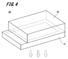
- FIG. 4 shows a schematic diagram of the organic EL element
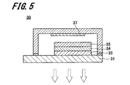
- FIG. 5 shows a cross-sectional view of the organic EL element.
- the organic EL element 30 shown in FIGS. 4 and 5 is covered with a glass substrate 31 and a glass cover 32.
- the sealing operation with the glass cover 32 was performed in a glove box (in an atmosphere of high-purity nitrogen gas having a purity of 99.999% or more) in a nitrogen atmosphere without bringing the organic EL element into contact with the air.
- a transparent electrode 33, a light emitting unit 34, and a cathode 35 are laminated on the glass substrate 31.
- the glass cover 32 is filled with nitrogen gas, and a water capturing agent 37 is provided.
- the vacuum deposition apparatus is depressurized to a vacuum degree of 1 ⁇ 10 ⁇ 4 Pa, and then heated by energizing the deposition crucible containing the compound M-1 represented by the following structural formula on a glass substrate at a deposition rate of 0.1 nm / second. To form a layer with a thickness of 15 nm.
- the compound M-2 represented by the following structural formula was vapor-deposited in the same manner to form a layer having a thickness of 50 nm.
- the compound RD-1 and the compound H-1 represented by the following structural formula were co-deposited at a deposition rate of 0.1 nm / second so that the compound RD-1 was 15%, and a red light emission with a film thickness of 30 nm was obtained.
- a phosphorescent light emitting layer (first light emitting layer) exhibiting the above was formed.
- Compound RD-1 is a light-emitting dopant having an emission peak near 605 nm.
- Compound BD-1 and Compound H-1 represented by the following structural formula as blue light emitting dopants were co-deposited at a deposition rate of 0.1 nm / second so that the concentration of Compound BD-1 was 5%, A fluorescent light emitting layer (second light emitting layer) exhibiting blue light emission with a film thickness of 30 nm was formed.
- Compound E-1 represented by the following structural formula was deposited at a deposition rate of 0.1 nm / second to form a 20 nm thick layer.
- Intermediate connector layer As an intermediate connector layer, the compound E-1 and NDN-26 manufactured by Novaled were co-deposited to a thickness of 25 nm at a deposition rate of 0.1 nm / second so that a concentration of 5% by mass was obtained. Formed. Thereby, the electron transport property which added the electron donor was formed.
- Compound M-2 and NDP-9 manufactured by Novaled were co-deposited at a deposition rate of 0.1 nm / second so as to have a volume ratio of 50:50 to form a layer having a thickness of 10 nm. Thereby, the hole transport property which added the electron-accepting substance was formed.
- Compound M-2 was deposited at a deposition rate of 0.1 nm / second to form a 50 nm thick layer.
- a compound GD-1 and a compound H-1 represented by the following structural formula as a green light emitting dopant were co-deposited at a deposition rate of 0.1 nm / second so that the compound GD-1 was 15%.
- a phosphorescent light emitting layer (third light emitting layer) exhibiting green emission of 30 nm was formed.
- the compound RD-2 and the compound H-1 represented by the following structural formula were co-deposited at a deposition rate of 0.1 nm / second so that the concentration of the compound RD-2 was 15%.
- a phosphorescent light emitting layer (fourth light emitting layer) exhibiting red light emission was formed.
- Compound RD-2 is a light-emitting dopant having an emission peak near 620 nm.
- Compound E-1 was deposited at a deposition rate of 0.1 nm / second to form a layer having a thickness of 35 nm.
- LiF was formed with a film thickness of 1.5 nm.
- Compound GD-1, Compound RD-2, and Compound H-1 were co-deposited at a deposition rate of 0.1 nm / second so that Compound GD-1 was 15% and Compound RD-2 was 1.5%.
- a phosphorescent light emitting layer having a film thickness of 30 nm and exhibiting green light emission and red light was formed.
- the deposition rate is 0 so that the compound GD-1, the compound RD-1, and the compound H-1 are 15% for the compound GD-1 and 1.5% for the compound RD-1.
- Compound BD-1, Compound RD-2, and Compound H-1 were co-deposited at a deposition rate of 0.1 nm / second so that Compound BD-1 was 15% and Compound RD-2 was 1.5%.
- a phosphorescent light emitting layer having a film thickness of 30 nm and exhibiting blue light emission and red light was formed.
- Compound E-1 was deposited at a deposition rate of 0.1 nm / second to form a layer having a thickness of 35 nm.
- LiF was formed with a film thickness of 1.5 nm.
- aluminum 110nm was vapor-deposited and the cathode was formed.
- Table 1 below shows the configurations of the organic EL elements of Samples 101 to 118.
- Samples 101 to 117 containing two types of light emitting dopants having a peak in a wavelength region of 580 nm or more have an average color rendering index as compared with Sample 118 containing only one type of light emitting dopant having a peak in a region of wavelength 580 nm or more.
- Ra and the special color rendering index R9 are improved.
- the average color rendering index Ra and the special color rendering index R9 are improved. Therefore, it can be understood that the average color rendering index Ra and the special color rendering index R9 of the organic EL element are improved by including two kinds of light emitting dopants having a peak in a wavelength region of 580 nm or more.
- Samples 101 to 117 and sample 118 include four types of light emitting dopants having different peak wavelengths, but samples 101 to 117 including two types of light emitting dopants having a peak in a region having a wavelength of 580 nm or more have a wavelength of 580 nm or more.
- samples 101 to 117 including two types of light emitting dopants having a peak in a region having a wavelength of 580 nm or more have a wavelength of 580 nm or more.
- the change in current density and the influence on chromaticity due to the passage of time are small, and it can be seen that the color change of the organic EL element is suppressed. .
- the light emission spectrum of light extracted from the organic EL element is distributed over a wide wavelength region by including two types of light emitting dopants having a peak in a wavelength region of 580 nm or more. It is possible to suppress the color change of the organic EL element.
- the sample 103 In the sample 103, the sample 106, the sample 107, the sample 110, and the sample 113, two types of light-emitting dopants having peaks in a region having a wavelength of 580 nm or more are included in the same light-emitting unit.
- the driving voltage is higher than that of the sample 101. This is presumably because the light-emitting unit contains only a light-emitting dopant having a peak in a region having a wavelength of 580 nm or longer, which has a low carrier transport property, and thus the carrier transport property of the light-emitting unit is lowered.
- the drive voltage is high.
- the driving voltage is not significantly increased. Therefore, it can be seen that the drive voltage can be lowered by including the light emitting dopant having a peak in the wavelength region of 580 nm or more and the other light emitting dopant in the same light emitting unit.
- Samples 101 and 102 having different positions of the light-emitting layer containing RD-1 having a peak wavelength of 605 nm and RD-2 having a peak wavelength of 620 nm as two types of light-emitting dopants having a peak in a wavelength region of 580 nm or more, When comparing the sample 104 and the sample 105, the power efficiency is improved in the sample 102 and the sample 105.
- Sample 101 and sample 104 are RD-2 having a peak wavelength of 620 nm on the fourth light-emitting layer of the second light-emitting unit formed on the most cathode side, out of two types of light-emitting dopants having a peak in a wavelength region of 580 nm or more. Is included.
- the sample 102 and the sample 105 have a configuration in which RD-1 is included in the fourth light emitting layer of the second light emitting unit formed on the most cathode side.
- plasmon loss can be suppressed by including RD-1 having a peak on the short wavelength side among the two types of light emitting dopants having a peak in a wavelength region of 580 nm or more in the cathode side light emitting layer. It is considered that the power efficiency of the organic EL element could be improved.
Landscapes
- Physics & Mathematics (AREA)
- Optics & Photonics (AREA)
- Electroluminescent Light Sources (AREA)
Abstract
Priority Applications (2)
| Application Number | Priority Date | Filing Date | Title |
|---|---|---|---|
| JP2016511471A JPWO2015151684A1 (ja) | 2014-04-03 | 2015-02-27 | 有機エレクトロルミネッセンス素子、及び、電子デバイス |
| US15/120,313 US9843008B2 (en) | 2014-04-03 | 2015-02-27 | Organic electroluminescent element and electronic device |
Applications Claiming Priority (2)
| Application Number | Priority Date | Filing Date | Title |
|---|---|---|---|
| JP2014076799 | 2014-04-03 | ||
| JP2014-076799 | 2014-04-03 |
Publications (1)
| Publication Number | Publication Date |
|---|---|
| WO2015151684A1 true WO2015151684A1 (fr) | 2015-10-08 |
Family
ID=54240017
Family Applications (1)
| Application Number | Title | Priority Date | Filing Date |
|---|---|---|---|
| PCT/JP2015/055902 Ceased WO2015151684A1 (fr) | 2014-04-03 | 2015-02-27 | Élément électroluminescent organique et dispositif électronique |
Country Status (3)
| Country | Link |
|---|---|
| US (1) | US9843008B2 (fr) |
| JP (1) | JPWO2015151684A1 (fr) |
| WO (1) | WO2015151684A1 (fr) |
Cited By (1)
| Publication number | Priority date | Publication date | Assignee | Title |
|---|---|---|---|---|
| WO2017006639A1 (fr) * | 2015-07-08 | 2017-01-12 | 株式会社カネカ | Panneau électroluminescent organique d'émission de lumière blanche et son procédé de fabrication |
Families Citing this family (3)
| Publication number | Priority date | Publication date | Assignee | Title |
|---|---|---|---|---|
| WO2018043763A1 (fr) | 2016-09-02 | 2018-03-08 | Kyushu University, National University Corporation | Laser à rétroaction distribuée à couche mince organique à onde continue et diode laser à semi-conducteur organique à commande électrique |
| JP6151846B1 (ja) * | 2016-12-27 | 2017-06-21 | Lumiotec株式会社 | 有機エレクトロルミネッセント素子、照明装置、ディスプレイ装置 |
| KR102105384B1 (ko) * | 2018-07-19 | 2020-04-28 | 삼성전기주식회사 | 적층형 커패시터 |
Citations (3)
| Publication number | Priority date | Publication date | Assignee | Title |
|---|---|---|---|---|
| WO2004077886A1 (fr) * | 2003-02-27 | 2004-09-10 | Kabushiki Kaisha Toyota Jidoshokki | Dispositif electroluminescent organique |
| JP2012204093A (ja) * | 2011-03-24 | 2012-10-22 | Panasonic Corp | 有機エレクトロルミネッセンス素子 |
| WO2013073169A1 (fr) * | 2011-11-15 | 2013-05-23 | 出光興産株式会社 | Elément électroluminescent organique blanc |
Family Cites Families (3)
| Publication number | Priority date | Publication date | Assignee | Title |
|---|---|---|---|---|
| KR101215279B1 (ko) | 2004-05-21 | 2012-12-26 | 가부시키가이샤 한도오따이 에네루기 켄큐쇼 | 조명 장치 |
| CN103890992A (zh) * | 2011-10-19 | 2014-06-25 | E.I.内穆尔杜邦公司 | 用于照明的有机电子装置 |
| JP5321700B2 (ja) * | 2012-01-17 | 2013-10-23 | 三菱化学株式会社 | 有機電界発光素子、有機el照明および有機el表示装置 |
-
2015
- 2015-02-27 JP JP2016511471A patent/JPWO2015151684A1/ja active Pending
- 2015-02-27 US US15/120,313 patent/US9843008B2/en not_active Expired - Fee Related
- 2015-02-27 WO PCT/JP2015/055902 patent/WO2015151684A1/fr not_active Ceased
Patent Citations (3)
| Publication number | Priority date | Publication date | Assignee | Title |
|---|---|---|---|---|
| WO2004077886A1 (fr) * | 2003-02-27 | 2004-09-10 | Kabushiki Kaisha Toyota Jidoshokki | Dispositif electroluminescent organique |
| JP2012204093A (ja) * | 2011-03-24 | 2012-10-22 | Panasonic Corp | 有機エレクトロルミネッセンス素子 |
| WO2013073169A1 (fr) * | 2011-11-15 | 2013-05-23 | 出光興産株式会社 | Elément électroluminescent organique blanc |
Non-Patent Citations (2)
| Title |
|---|
| SHIGERU IKAWA ET AL.: "White polymer light- emitting diodesco-doped with phosphorescentiridium complexes bearing the same cyclometalated ligand", PHYSICA STATUS SOLIDI C, vol. 9, no. 12, pages 2553 - 2556, XP055229162, ISSN: 1862-6351 * |
| YANG LI ET AL.: "Ultra-high general and special color rendering index white organic light- emitting device based on a deep red phosphorescent dye", ORGANIC ELECTRONICS, vol. 14, 2013, pages 3201 - 3205, XP028778239, ISSN: 1566-1199 * |
Cited By (3)
| Publication number | Priority date | Publication date | Assignee | Title |
|---|---|---|---|---|
| WO2017006639A1 (fr) * | 2015-07-08 | 2017-01-12 | 株式会社カネカ | Panneau électroluminescent organique d'émission de lumière blanche et son procédé de fabrication |
| JP6078701B1 (ja) * | 2015-07-08 | 2017-02-08 | 株式会社カネカ | 白色発光有機elパネル及びその製造方法 |
| US10026918B2 (en) | 2015-07-08 | 2018-07-17 | Kaneka Corporation | White light emitting organic EL panel and method for producing same |
Also Published As
| Publication number | Publication date |
|---|---|
| JPWO2015151684A1 (ja) | 2017-04-13 |
| US9843008B2 (en) | 2017-12-12 |
| US20170069863A1 (en) | 2017-03-09 |
Similar Documents
| Publication | Publication Date | Title |
|---|---|---|
| JP6307993B2 (ja) | 有機エレクトロルミネッセンス素子、及び、電子デバイス | |
| US11329234B2 (en) | Organic electroluminescent element, display device, lighting device, π-conjugated compound, and light-emitting thin film | |
| US11910628B2 (en) | Luminescent film, organic electroluminescent element, organic material composition and method for producing organic electroluminescent element | |
| CN109155370B (zh) | 有机电致发光元件用材料、有机电致发光元件、显示装置及照明装置 | |
| US10651395B2 (en) | Organic electroluminescent element, display device, and illumination device | |
| US20160285008A1 (en) | Organic electroluminescent element, display device, and lighting device | |
| JP6417821B2 (ja) | 有機エレクトロルミネッセンス素子及び照明装置 | |
| JP6146415B2 (ja) | 有機エレクトロルミネッセンス素子、照明装置及び表示装置 | |
| KR20170082447A (ko) | 유기 일렉트로루미네센스 소자, 유기 일렉트로루미네센스 소자의 제조 방법, 표시 장치 및 조명 장치 | |
| CN107534092A (zh) | 有机电致发光元件用材料、有机电致发光元件、显示装置及照明装置 | |
| JP5151031B2 (ja) | 有機エレクトロルミネッセンス素子、表示装置及び照明装置 | |
| JPWO2015087795A1 (ja) | 有機エレクトロルミネッセンス素子、照明装置及び表示装置 | |
| JP5051125B2 (ja) | 有機エレクトロルミネッセンス素子、有機エレクトロルミネッセンス素子の発光色度安定化方法、照明装置及び電子ディスプレイ装置 | |
| JP2016225498A (ja) | 有機エレクトロルミネッセンス素子 | |
| JPWO2009008367A1 (ja) | 有機エレクトロルミネッセンス素子材料、有機エレクトロルミネッセンス素子、表示装置及び照明装置 | |
| US9843008B2 (en) | Organic electroluminescent element and electronic device | |
| US20200127210A1 (en) | Organic electroluminescent element material, organic electroluminescent element, display device, lighting device, and compound | |
| JP2021166212A (ja) | 有機エレクトロルミネッセンス素子 | |
| WO2018116923A1 (fr) | Électrode transparente et dispositif électronique | |
| JP2017212152A (ja) | 有機エレクトロルミネッセンス素子及びその製造方法 | |
| JP2016072586A (ja) | 有機エレクトロルミネッセンス素子 | |
| JP2017084562A (ja) | 有機エレクトロルミネッセンス素子及びその製造方法 |
Legal Events
| Date | Code | Title | Description |
|---|---|---|---|
| 121 | Ep: the epo has been informed by wipo that ep was designated in this application |
Ref document number: 15772690 Country of ref document: EP Kind code of ref document: A1 |
|
| WWE | Wipo information: entry into national phase |
Ref document number: 15120313 Country of ref document: US |
|
| ENP | Entry into the national phase |
Ref document number: 2016511471 Country of ref document: JP Kind code of ref document: A |
|
| NENP | Non-entry into the national phase |
Ref country code: DE |
|
| 122 | Ep: pct application non-entry in european phase |
Ref document number: 15772690 Country of ref document: EP Kind code of ref document: A1 |