WO2015151978A1 - Élément de commande de lumière - Google Patents
Élément de commande de lumière Download PDFInfo
- Publication number
- WO2015151978A1 WO2015151978A1 PCT/JP2015/059234 JP2015059234W WO2015151978A1 WO 2015151978 A1 WO2015151978 A1 WO 2015151978A1 JP 2015059234 W JP2015059234 W JP 2015059234W WO 2015151978 A1 WO2015151978 A1 WO 2015151978A1
- Authority
- WO
- WIPO (PCT)
- Prior art keywords
- control element
- electrode
- signal
- light control
- electrodes
- Prior art date
- Legal status (The legal status is an assumption and is not a legal conclusion. Google has not performed a legal analysis and makes no representation as to the accuracy of the status listed.)
- Ceased
Links
Images


Classifications
-
- G—PHYSICS
- G02—OPTICS
- G02F—OPTICAL DEVICES OR ARRANGEMENTS FOR THE CONTROL OF LIGHT BY MODIFICATION OF THE OPTICAL PROPERTIES OF THE MEDIA OF THE ELEMENTS INVOLVED THEREIN; NON-LINEAR OPTICS; FREQUENCY-CHANGING OF LIGHT; OPTICAL LOGIC ELEMENTS; OPTICAL ANALOGUE/DIGITAL CONVERTERS
- G02F1/00—Devices or arrangements for the control of the intensity, colour, phase, polarisation or direction of light arriving from an independent light source, e.g. switching, gating or modulating; Non-linear optics
- G02F1/01—Devices or arrangements for the control of the intensity, colour, phase, polarisation or direction of light arriving from an independent light source, e.g. switching, gating or modulating; Non-linear optics for the control of the intensity, phase, polarisation or colour
- G02F1/21—Devices or arrangements for the control of the intensity, colour, phase, polarisation or direction of light arriving from an independent light source, e.g. switching, gating or modulating; Non-linear optics for the control of the intensity, phase, polarisation or colour by interference
- G02F1/225—Devices or arrangements for the control of the intensity, colour, phase, polarisation or direction of light arriving from an independent light source, e.g. switching, gating or modulating; Non-linear optics for the control of the intensity, phase, polarisation or colour by interference in an optical waveguide structure
-
- G—PHYSICS
- G02—OPTICS
- G02F—OPTICAL DEVICES OR ARRANGEMENTS FOR THE CONTROL OF LIGHT BY MODIFICATION OF THE OPTICAL PROPERTIES OF THE MEDIA OF THE ELEMENTS INVOLVED THEREIN; NON-LINEAR OPTICS; FREQUENCY-CHANGING OF LIGHT; OPTICAL LOGIC ELEMENTS; OPTICAL ANALOGUE/DIGITAL CONVERTERS
- G02F1/00—Devices or arrangements for the control of the intensity, colour, phase, polarisation or direction of light arriving from an independent light source, e.g. switching, gating or modulating; Non-linear optics
- G02F1/01—Devices or arrangements for the control of the intensity, colour, phase, polarisation or direction of light arriving from an independent light source, e.g. switching, gating or modulating; Non-linear optics for the control of the intensity, phase, polarisation or colour
- G02F1/21—Devices or arrangements for the control of the intensity, colour, phase, polarisation or direction of light arriving from an independent light source, e.g. switching, gating or modulating; Non-linear optics for the control of the intensity, phase, polarisation or colour by interference
- G02F1/212—Mach-Zehnder type
Definitions
- the present invention relates to a light control element, and more particularly, to a light control element having two or more signal electrodes in a modulation electrode.
- An optical control element in which an optical waveguide and a modulation electrode are formed on a substrate having an electro-optic effect such as lithium niobate, and a light wave propagating through the optical waveguide is modulated by the modulation electrode has been put into practical use.
- DQPSK modulation differential quadrature phase shift keying
- a Mach-Zehnder type optical waveguide (MZ type optical waveguide) is driven by a plurality of modulation signals.
- an integrated modulator including a plurality of signal electrodes for coherent multilevel communication such as a DP-QPSK modulator using polarization synthesis is also used.
- a light control element having a plurality of optical waveguides and a plurality of signal electrodes
- different modulation signals are often inputted to the respective signal electrodes, and different modulation signals are applied to the respective optical waveguides. It is configured. For this reason, when an electric field other than a predetermined modulation signal acts on a specific optical waveguide, optical characteristics of the light control element such as the extinction ratio of the signal light deteriorate. Such a phenomenon is called crosstalk.
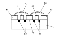
- FIGS. 1 and 2 are a light control element in which two or more signal electrodes (31, 32) are arranged. Proposed bonding the ground electrodes (41, 42, 43) to each other with gold wires (51, 52).
- This proposal has shown that the high-frequency ground potential of the working part is stabilized, crosstalk between the electrodes is suppressed, and stable modulation operation is possible at a wide band frequency.
- FIG. 2 is a cross-sectional view taken along one-dot chain line A-A ′ in FIG. Reference numerals other than those described above indicate the substrate 1, optical waveguides (21 to 23), ground electrodes (44 to 46), and bonding connection lines (53, 54) such as gold wires.
- the bonding part bonds a bonding wire such as gold with ultrasonic waves (thermal ultrasonic pressure bonding) using a needle-shaped bonding tool.
- a thin gold wire generally used is 20 to 30 ⁇ m, and even in that case, a space of about 100 ⁇ m is required as a bonding portion.
- JP 2009-53444 A Japanese Patent No. 5067464
- the problem to be solved by the present invention is to solve the above-described problems and provide a light control element capable of suppressing crosstalk between electrodes even if the light control element is narrowed. It is.
- the light control element of the present invention has the following technical features.
- the modulation electrode includes at least two signals.
- An electrode and a ground electrode arranged so as to sandwich the signal electrode, and the modulation electrode exerting a modulation action on the light wave is disposed between the two signal electrodes.
- the ground electrode is electrically connected to the other ground electrode, and an electrical connection means is provided so as to straddle a part of the signal electrode, and the electrical connection means includes at least A plurality of ground electrodes are connected by a single conductive line.
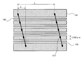
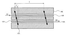
- the electrical connection means arranges a plurality of the conductive lines, and an interval L between adjacent conductive lines with respect to a direction in which the signal electrode extends. Is set to be less than a quarter of the wavelength ⁇ at the frequency of the modulation signal propagating through the signal electrode.
- the electrical connection means arranges a plurality of the conductive wires, and a distance L between adjacent conductive wires in the direction in which the signal electrode extends. Is set to be less than one-tenth with respect to the wavelength ⁇ at the frequency of the modulation signal propagating through the signal electrode.
- At least a part of a portion where the one conductive wire and the ground electrode are connected is a width of the ground electrode. Is 200 ⁇ m or less.
- the present invention relates to a light control element including a substrate having an electro-optic effect, an optical waveguide formed on the substrate, and a modulation electrode that modulates a light wave propagating through the optical waveguide.
- the modulation electrode includes at least two modulation electrodes. It is composed of a signal electrode and a ground electrode arranged so as to sandwich the signal electrode, and the modulation electrode exerts a modulation action on the light wave, and the modulation electrode is disposed between the two signal electrodes.
- the electrical connecting means arranges a plurality of conductive lines, and the interval L between the conductive lines adjacent to the direction in which the signal electrodes extend propagates through the signal electrodes.
- the distance L between adjacent conductive lines and the length L ′ of each straight line connecting the both ends of the conductive lines with respect to the direction L satisfy the relationship L> L ′.
- the potential between the ground electrodes can be maintained substantially the same, and good signal quality with suppressed crosstalk (for example, variation in frequency characteristics is reduced and stability is increased) is obtained. be able to.
- the above-described length L ′ is also less than a quarter of the wavelength ⁇ , and more preferably one-tenth or less, so that the conductive wire is disposed perpendicular to the direction in which the signal electrode extends. It is possible to suppress crosstalk to the same extent as.
- At least a part of a portion where one conductive line and the ground electrode are connected can achieve a good connection state even when the width of the ground electrode is 200 ⁇ m or less. it can.
- a sufficient connection region can be ensured by arranging the conductive lines obliquely with respect to the direction in which the signal electrodes extend.
- FIG. 10 is a plan view showing an outline of a light control element disclosed in Patent Document 2.
- FIG. FIG. 2 is a cross-sectional view taken along one-dot chain line A-A ′ in FIG. 1. It is a top view concerning the light control element of one mode of the present invention.
- FIG. 4 is a cross-sectional view taken along one-dot chain line AA ′ in FIG. 3. It is the figure which expanded a part of modulation electrode of FIG. It is a figure which shows the other Example of the light control element of 1 aspect of this invention, and is a figure explaining the arrangement
- FIG. 8 is a graph showing the influence of crosstalk when the inclination of the conductive line is changed in the direction in which the signal electrode extends in the light control element of FIG. 7.
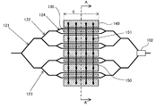
- FIG. 3 is a schematic view of a light control element to which the present invention is applied
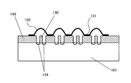
- FIG. 4 is a cross-sectional view taken along the alternate long and short dash line AA ′ in FIG.
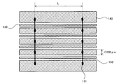
- FIG. 5 is an enlarged view of the modulation electrode portion of FIG.
- the light control element of the present invention modulates a substrate 101 having an electro-optic effect, an optical waveguide (121 to 124) formed on the substrate, and a light wave propagating through the optical waveguide.
- the modulation electrode is composed of at least two signal electrodes 130 and a ground electrode 140 disposed so as to sandwich the signal electrode, and the modulation electrode modulates the light wave.
- the working portion S of the modulation electrode is electrically connected to the ground electrode disposed between the two signal electrodes and the other ground electrode, and a part of the signal electrode.
- An electrical connection means arranged so as to straddle is provided, and the electrical connection means is configured to connect at least a plurality of ground electrodes with a single conductive line 150.
- the substrate 1 having an electro-optic effect a single crystal of any one of LiNbO 3 , LiTaO 5 or PLZT (lead lanthanum zirconate titanate) can be suitably used.
- LiNbO 3 and LiTaO 5 frequently used in light control elements such as an optical modulator are preferable.
- the optical waveguide formed on the substrate is formed, for example, by thermally diffusing a high refractive index material such as titanium (Ti) on a LiNbO 3 substrate (LN substrate).
- a ridge-type optical waveguide in which irregularities along the optical waveguide are formed on the substrate can also be used.
- the light control element using the X-cut type substrate is illustrated in FIG. 3, the present invention is not limited to this and can be similarly applied to a Z-cut type substrate.
- FIG. 3 illustrates an optical waveguide used in the DP-QPSK modulator.
- Two second MZ type optical waveguides (122, 123) are inserted into the branching waveguide of the first Mach-Zehnder type optical waveguide (MZ type optical waveguide) 121, and the second MZ type optical waveguide is further branched.
- Four third MZ type optical waveguides 124 are inserted in the waveguide.
- the combining unit 102 of the first MZ type optical waveguide 121 is formed with a polarization combining unit so as to combine two output lights to be combined while changing the polarization plane.
- the light control element of the present invention is not limited to such an optical waveguide, but a crosstalk phenomenon is likely to occur in a light control element having a plurality of light modulation units, and therefore the configuration of the present invention is applied. Superiority.
- the modulation electrode is composed of a signal electrode 130 and a ground electrode 140, and a Ti / Au electrode pattern is formed on the surface of the substrate, and can be formed by a gold plating method or the like. Furthermore, if necessary, a buffer layer such as dielectric SiO 2 can be provided on the surface of the substrate after the optical waveguide is formed, and a modulation electrode can be formed above the buffer layer. It is particularly preferable that the light control element to which the present invention is applied has a configuration in which a ground electrode is disposed between a plurality of signal electrodes.
- a plurality of signal electrodes to which a microwave signal is applied are arranged so that the ground electrode is sandwiched, and the electric field formed by the modulation electrode is applied to the optical waveguide.
- the plurality of ground electrodes are continuously connected (wire bonding) with one conductive wire.
- one conductive wire 250 is used to connect a plurality of ground electrodes 240, and the conductive wires are bonded on each ground electrode 240 with ultrasonic waves.
- a plurality of conductive wires connected in this way are arranged in parallel as necessary.
- the bonding distance required for one ground electrode can be reduced.
- the manufacturing time of the light control element can be shortened.
- the reduction in the number of bondings also reduces damage to the substrate due to bonding.
- the width of the ground electrode sandwiched between the signal electrodes becomes increasingly narrower.
- the present invention can be preferably applied to a case where the width of the ground electrode in the portion to which the conductive line is connected is 200 ⁇ m or less. The reason is that the area required for connection can be minimized by connecting with one conductive line.
- a wider connection area can be secured. Even in a light control element miniaturized by this configuration, the ground potential of the ground electrodes on both sides of the signal electrode is stabilized, crosstalk between the signal electrodes is suppressed, and good modulation signal quality can be obtained.
- a conductive wire having a high conductivity such as a gold wire can be used.
- the conductive wire has as low a loop height as possible (the height of the conductive wire across the signal electrode from the substrate) and the length of the conductive wire is short.
- the length of the conductive wire between the bonding point and the adjacent bonding point is preferably 1 mm or less, more preferably 0.5 mm or less while maintaining a length that does not cause a short between the conductive wire and the signal electrode. Good.
- the interval L between the conductive lines is set to less than a quarter of the wavelength ⁇ at the frequency of the modulation signal propagating through the signal electrode. Also good. With this configuration, it is possible to prevent the electric field from the signal electrode from leaking beyond the ground electrode. More preferably, the crosstalk can be reliably suppressed by setting the interval L to 1/10 or less of the wavelength of the electric signal. In addition, since the electric field formed by the signal electrode is efficiently applied to the optical waveguide, a decrease in modulation efficiency in a wideband frequency is suppressed, and the frequency characteristics can be improved.
- the conductive wire should be perpendicular to the direction in which the signal electricity extends. Need to be placed.
- the length L ′ indicating the inclination of the conductive line with respect to the direction is set to L> L ′, and similarly to the interval L, the length L ′ is set to the wavelength ⁇ at the frequency of the modulation signal propagating through the signal electrode.
- the light control element is usually housed in a metal case and modularized.
- the ground electrode near the side surface of the light control element is connected to the ground side terminal of the signal line introduced from the metal case or the outside.
- the electrical connection means is provided at the action portion where the modulation electrode exerts a modulation action on the light wave. This is because it is necessary to most suppress the crosstalk phenomenon in the action portion. Further, such an action part is present in the vicinity of the center of the substrate of the light control element, and is often located farthest from the place where the ground electrode is grounded to the metal case of the module. For this reason, since it is difficult to ensure a sufficient grounding state, it is necessary to reinforce and stabilize the grounding state using the electrical connection means as in the present invention.
- the signal S1 is input from the left end of the signal electrode 130 and absorbed by the terminator at the right end.
- the left end of the signal electrode 131 is connected to a terminator, and the signal S2 output from the right end is measured. The result is shown in FIG.
Landscapes
- Physics & Mathematics (AREA)
- Nonlinear Science (AREA)
- General Physics & Mathematics (AREA)
- Optics & Photonics (AREA)
- Optical Modulation, Optical Deflection, Nonlinear Optics, Optical Demodulation, Optical Logic Elements (AREA)
Abstract
L'invention vise à fournir un élément de commande de lumière qui permet de réduire la diaphonie inter-électrode même si la largeur dudit élément de commande de lumière est réduite. Ledit élément de commande de lumière, qui a un substrat qui présente un effet électro-optique, des guides d'onde optiques (121 à 124) formés sur ledit substrat, et des électrodes de modulation qui modulent des ondes lumineuses se propageant à travers lesdits guides d'onde optiques, est caractérisé en ce que : les électrodes de modulation comprennent deux électrodes de signal (130) ou plus et des électrodes de masse (140) disposées de manière à prendre en sandwich lesdites électrodes de signal ; une section d'action (S) des électrodes de modulation, ladite section d'action (S) étant la section où les électrodes de modulation exercent un effet de modulation sur les ondes lumineuses, qui comprend un moyen de connexion électrique qui est disposé de façon à chevaucher des parties des électrodes de signal et connecte électriquement les électrodes de masse disposées entre des électrodes de signal avec les autres électrodes de masse ; et lesdits moyens de connexion électrique sont conçus de manière à relier au moins une pluralité d'électrodes de masse les unes avec les autres par l'intermédiaire d'un fil conducteur unique (150).
Applications Claiming Priority (2)
| Application Number | Priority Date | Filing Date | Title |
|---|---|---|---|
| JP2014-073504 | 2014-03-31 | ||
| JP2014073504A JP5991339B2 (ja) | 2014-03-31 | 2014-03-31 | 光制御素子 |
Publications (1)
| Publication Number | Publication Date |
|---|---|
| WO2015151978A1 true WO2015151978A1 (fr) | 2015-10-08 |
Family
ID=54240304
Family Applications (1)
| Application Number | Title | Priority Date | Filing Date |
|---|---|---|---|
| PCT/JP2015/059234 Ceased WO2015151978A1 (fr) | 2014-03-31 | 2015-03-25 | Élément de commande de lumière |
Country Status (2)
| Country | Link |
|---|---|
| JP (1) | JP5991339B2 (fr) |
| WO (1) | WO2015151978A1 (fr) |
Cited By (5)
| Publication number | Priority date | Publication date | Assignee | Title |
|---|---|---|---|---|
| WO2018002658A1 (fr) * | 2016-07-01 | 2018-01-04 | Oclaro Technology Limited | Structure de mise à la masse dans un réseau de guides d'ondes rf |
| EP3432059A4 (fr) * | 2016-03-18 | 2019-10-30 | Nippon Telegraph and Telephone Corporation | Modulateur optique |
| EP3432058A4 (fr) * | 2016-03-18 | 2019-11-06 | Nippon Telegraph And Telephone Corporation | Modulateur optique |
| US10678114B2 (en) | 2016-07-01 | 2020-06-09 | Lumentum Technology Uk Limited | Ground structure in RF waveguide array |
| CN111936919A (zh) * | 2018-03-30 | 2020-11-13 | 住友大阪水泥株式会社 | 光波导元件 |
Families Citing this family (3)
| Publication number | Priority date | Publication date | Assignee | Title |
|---|---|---|---|---|
| JP6603571B2 (ja) * | 2015-12-17 | 2019-11-06 | 日本電信電話株式会社 | 光変調器 |
| JP7052444B2 (ja) * | 2018-03-15 | 2022-04-12 | 住友大阪セメント株式会社 | 光変調器、及び光伝送装置 |
| JP7283180B2 (ja) * | 2019-03-29 | 2023-05-30 | 住友大阪セメント株式会社 | 光変調器 |
Citations (4)
| Publication number | Priority date | Publication date | Assignee | Title |
|---|---|---|---|---|
| US6192167B1 (en) * | 1998-07-24 | 2001-02-20 | Uniphase Telecommunications Products | Differential drive optical modulator |
| US20030228081A1 (en) * | 2002-05-02 | 2003-12-11 | Tavlykaev Robert F. | Optical modulators with coplanar-waveguide-to-coplanar-strip electrode transitions |
| JP2012078496A (ja) * | 2010-09-30 | 2012-04-19 | Sumitomo Osaka Cement Co Ltd | 光制御素子 |
| JP2012163882A (ja) * | 2011-02-09 | 2012-08-30 | Anritsu Corp | 光変調器 |
-
2014
- 2014-03-31 JP JP2014073504A patent/JP5991339B2/ja active Active
-
2015
- 2015-03-25 WO PCT/JP2015/059234 patent/WO2015151978A1/fr not_active Ceased
Patent Citations (4)
| Publication number | Priority date | Publication date | Assignee | Title |
|---|---|---|---|---|
| US6192167B1 (en) * | 1998-07-24 | 2001-02-20 | Uniphase Telecommunications Products | Differential drive optical modulator |
| US20030228081A1 (en) * | 2002-05-02 | 2003-12-11 | Tavlykaev Robert F. | Optical modulators with coplanar-waveguide-to-coplanar-strip electrode transitions |
| JP2012078496A (ja) * | 2010-09-30 | 2012-04-19 | Sumitomo Osaka Cement Co Ltd | 光制御素子 |
| JP2012163882A (ja) * | 2011-02-09 | 2012-08-30 | Anritsu Corp | 光変調器 |
Cited By (9)
| Publication number | Priority date | Publication date | Assignee | Title |
|---|---|---|---|---|
| EP3432059A4 (fr) * | 2016-03-18 | 2019-10-30 | Nippon Telegraph and Telephone Corporation | Modulateur optique |
| EP3432058A4 (fr) * | 2016-03-18 | 2019-11-06 | Nippon Telegraph And Telephone Corporation | Modulateur optique |
| US10852618B2 (en) | 2016-03-18 | 2020-12-01 | Nippon Telegraph And Telephone Corporation | Optical modulator having interconnecting ground electrodes for coplanar waveguides |
| US10890787B2 (en) | 2016-03-18 | 2021-01-12 | Nippon Telegraph And Telephone Corporation | Optical modulator |
| WO2018002658A1 (fr) * | 2016-07-01 | 2018-01-04 | Oclaro Technology Limited | Structure de mise à la masse dans un réseau de guides d'ondes rf |
| US10678114B2 (en) | 2016-07-01 | 2020-06-09 | Lumentum Technology Uk Limited | Ground structure in RF waveguide array |
| US10684528B2 (en) | 2016-07-01 | 2020-06-16 | Lumentum Technology Uk Limited | Ground structure in RF waveguide array |
| CN111936919A (zh) * | 2018-03-30 | 2020-11-13 | 住友大阪水泥株式会社 | 光波导元件 |
| CN111936919B (zh) * | 2018-03-30 | 2024-01-02 | 住友大阪水泥株式会社 | 光波导元件 |
Also Published As
| Publication number | Publication date |
|---|---|
| JP5991339B2 (ja) | 2016-09-14 |
| JP2015197452A (ja) | 2015-11-09 |
Similar Documents
| Publication | Publication Date | Title |
|---|---|---|
| JP5991339B2 (ja) | 光制御素子 | |
| JP5067464B2 (ja) | 光制御素子 | |
| US8135242B2 (en) | Optical modulator | |
| JP5171808B2 (ja) | 光位相変調器 | |
| US7643708B2 (en) | Optical modulator | |
| JP2008191614A (ja) | 光変調器 | |
| US10228605B2 (en) | Waveguide optical element | |
| JP2008089936A (ja) | 光制御素子 | |
| JP2014197054A (ja) | 光変調器 | |
| US10088699B2 (en) | Optical modulator | |
| JP4899730B2 (ja) | 光変調器 | |
| WO2017171094A1 (fr) | Modulateur optique | |
| JP2016212130A (ja) | 光変調器 | |
| JP5691747B2 (ja) | 進行波型光変調素子 | |
| JP6290971B2 (ja) | 光送信装置及び光変調器 | |
| JP6728888B2 (ja) | 光変調器 | |
| JP6729133B2 (ja) | 光変調器 | |
| JP2007093742A (ja) | 光変調器 | |
| JP6638515B2 (ja) | 光変調器 | |
| JP6288153B2 (ja) | 光変調器 | |
| JP2018077545A (ja) | 光送信装置 | |
| JP2013130833A (ja) | 光変調器 |
Legal Events
| Date | Code | Title | Description |
|---|---|---|---|
| 121 | Ep: the epo has been informed by wipo that ep was designated in this application |
Ref document number: 15773544 Country of ref document: EP Kind code of ref document: A1 |
|
| NENP | Non-entry into the national phase | ||
| 122 | Ep: pct application non-entry in european phase |
Ref document number: 15773544 Country of ref document: EP Kind code of ref document: A1 |