WO2015156142A1 - 画像処理装置 - Google Patents
画像処理装置 Download PDFInfo
- Publication number
- WO2015156142A1 WO2015156142A1 PCT/JP2015/059360 JP2015059360W WO2015156142A1 WO 2015156142 A1 WO2015156142 A1 WO 2015156142A1 JP 2015059360 W JP2015059360 W JP 2015059360W WO 2015156142 A1 WO2015156142 A1 WO 2015156142A1
- Authority
- WO
- WIPO (PCT)
- Prior art keywords
- pixel
- value
- signal
- pixel signal
- imaging period
- Prior art date
- Legal status (The legal status is an assumption and is not a legal conclusion. Google has not performed a legal analysis and makes no representation as to the accuracy of the status listed.)
- Ceased
Links
Images



Classifications
-
- G—PHYSICS
- G06—COMPUTING OR CALCULATING; COUNTING
- G06T—IMAGE DATA PROCESSING OR GENERATION, IN GENERAL
- G06T5/00—Image enhancement or restoration
- G06T5/70—Denoising; Smoothing
-
- H—ELECTRICITY
- H04—ELECTRIC COMMUNICATION TECHNIQUE
- H04N—PICTORIAL COMMUNICATION, e.g. TELEVISION
- H04N23/00—Cameras or camera modules comprising electronic image sensors; Control thereof
- H04N23/60—Control of cameras or camera modules
- H04N23/68—Control of cameras or camera modules for stable pick-up of the scene, e.g. compensating for camera body vibrations
- H04N23/682—Vibration or motion blur correction
- H04N23/684—Vibration or motion blur correction performed by controlling the image sensor readout, e.g. by controlling the integration time
-
- G—PHYSICS
- G06—COMPUTING OR CALCULATING; COUNTING
- G06T—IMAGE DATA PROCESSING OR GENERATION, IN GENERAL
- G06T7/00—Image analysis
- G06T7/20—Analysis of motion
- G06T7/223—Analysis of motion using block-matching
-
- H—ELECTRICITY
- H04—ELECTRIC COMMUNICATION TECHNIQUE
- H04N—PICTORIAL COMMUNICATION, e.g. TELEVISION
- H04N23/00—Cameras or camera modules comprising electronic image sensors; Control thereof
- H04N23/10—Cameras or camera modules comprising electronic image sensors; Control thereof for generating image signals from different wavelengths
- H04N23/12—Cameras or camera modules comprising electronic image sensors; Control thereof for generating image signals from different wavelengths with one sensor only
-
- H—ELECTRICITY
- H04—ELECTRIC COMMUNICATION TECHNIQUE
- H04N—PICTORIAL COMMUNICATION, e.g. TELEVISION
- H04N23/00—Cameras or camera modules comprising electronic image sensors; Control thereof
- H04N23/50—Constructional details
- H04N23/555—Constructional details for picking-up images in sites, inaccessible due to their dimensions or hazardous conditions, e.g. endoscopes or borescopes
-
- H—ELECTRICITY
- H04—ELECTRIC COMMUNICATION TECHNIQUE
- H04N—PICTORIAL COMMUNICATION, e.g. TELEVISION
- H04N23/00—Cameras or camera modules comprising electronic image sensors; Control thereof
- H04N23/60—Control of cameras or camera modules
- H04N23/61—Control of cameras or camera modules based on recognised objects
-
- H—ELECTRICITY
- H04—ELECTRIC COMMUNICATION TECHNIQUE
- H04N—PICTORIAL COMMUNICATION, e.g. TELEVISION
- H04N23/00—Cameras or camera modules comprising electronic image sensors; Control thereof
- H04N23/60—Control of cameras or camera modules
- H04N23/68—Control of cameras or camera modules for stable pick-up of the scene, e.g. compensating for camera body vibrations
- H04N23/681—Motion detection
- H04N23/6811—Motion detection based on the image signal
-
- H—ELECTRICITY
- H04—ELECTRIC COMMUNICATION TECHNIQUE
- H04N—PICTORIAL COMMUNICATION, e.g. TELEVISION
- H04N23/00—Cameras or camera modules comprising electronic image sensors; Control thereof
- H04N23/80—Camera processing pipelines; Components thereof
- H04N23/81—Camera processing pipelines; Components thereof for suppressing or minimising disturbance in the image signal generation
-
- H—ELECTRICITY
- H04—ELECTRIC COMMUNICATION TECHNIQUE
- H04N—PICTORIAL COMMUNICATION, e.g. TELEVISION
- H04N5/00—Details of television systems
- H04N5/14—Picture signal circuitry for video frequency region
- H04N5/21—Circuitry for suppressing or minimising disturbance, e.g. moiré or halo
-
- G—PHYSICS
- G06—COMPUTING OR CALCULATING; COUNTING
- G06T—IMAGE DATA PROCESSING OR GENERATION, IN GENERAL
- G06T2207/00—Indexing scheme for image analysis or image enhancement
- G06T2207/20—Special algorithmic details
- G06T2207/20172—Image enhancement details
- G06T2207/20182—Noise reduction or smoothing in the temporal domain; Spatio-temporal filtering
-
- H—ELECTRICITY
- H04—ELECTRIC COMMUNICATION TECHNIQUE
- H04N—PICTORIAL COMMUNICATION, e.g. TELEVISION
- H04N5/00—Details of television systems
- H04N5/14—Picture signal circuitry for video frequency region
- H04N5/144—Movement detection
Definitions
- the present invention relates to an image processing apparatus that generates an image by processing a signal output from an image sensor.
- Patent Document 1 Japanese Patent Laid-Open No. 2000-209507
- the image processing apparatus described in Patent Document 1 includes a cyclic noise reduction circuit.
- the cyclic noise reduction circuit described in Patent Document 1 takes a difference between a current video signal output from an image sensor and a video signal one frame before or one field before by a subtractor, and converts the difference to a difference value by a multiplier.
- the noise component is reduced from the video signal, and the feedback coefficient is controlled in units of one pixel according to the difference value from the subtractor. .
- the difference value from the subtractor increases, the feedback coefficient is reduced to reduce the afterimage, and as the difference value is decreased, the feedback coefficient is increased to reduce noise.
- the present invention has been made in view of the above circumstances, and an object thereof is to provide an image processing apparatus suitable for reducing noise in an image while suppressing an afterimage of a moving subject. is there.
- the image processing apparatus includes a pixel signal of the current imaging period output from the imaging element and 1 for each pixel in the effective pixel area of the imaging element that periodically images a subject in a predetermined imaging period.
- a difference value calculating means for calculating a difference value from the pixel signal of the previous imaging period, a first motion detecting means for detecting the motion of the subject within the entire effective pixel area, and each pixel in the effective pixel area.
- a pixel-of-interest setting unit that sequentially sets the pixel of interest, a second motion detection unit that detects a movement of the subject within a local pixel region including the pixel of interest that is sequentially set, and a first motion detection for each pixel of interest
- a mixture ratio determining means for determining a mixture ratio between a pixel signal in the current imaging period and a pixel signal in the previous imaging period based on the detection result by the means and the detection result by the second motion detection means; For, on the basis of the mixing ratio determined by the mixing ratio determination unit and a pixel signal correction means for correcting the pixel signal of the current imaging period.
- the image processing apparatus provides the pixel signal of the current imaging period output from the imaging device for each pixel in the effective pixel area of the imaging device that periodically images the subject in a predetermined imaging period.
- Difference value calculating means for calculating a difference value between the pixel signal and the pixel signal of the previous imaging period, and counting the number of pixels in which the difference value satisfies the first condition in the effective pixel region.
- a second count unit that counts values that satisfy the second condition and sets the number of counted pixels as a second count value; and for each target pixel, a second count in the pixel group to which the target pixel belongs.
- a mixing ratio determining unit that determines a mixing ratio between the pixel signal of the current imaging period and the pixel signal of the previous imaging period based on the current value and the first count value; Pixel signal correcting means for correcting the pixel signal of the current imaging period based on the determined mixture ratio.
- the mixing ratio determining unit may convert the first count value to the first value and convert the second count value to the second value. In this case, the mixture ratio determining unit determines the mixture ratio between the pixel signal in the current imaging period and the pixel signal in the previous imaging period based on the difference value between the first value and the second value.
- the numerical range of the first value and the numerical range of the second value may be the same.
- the first condition is, for example, that the difference value calculated by the difference value calculating means is larger than the first threshold value.
- the second condition is, for example, that the difference value is smaller than the second threshold value.
- the first count value is converted to the maximum value within the numerical range when the value is equal to or less than a certain value, and the first count value is converted to a value that is smaller than the maximum value as the value is larger than the certain value. Further, the second count value is converted into a value as it is.
- the mixing ratio determining means determines the mixing ratio based on the first value and the second value when the difference value between the first value and the second value is greater than or equal to the third threshold value. When the difference value between the value and the second value is less than the third threshold value, the mixing ratio is determined based on the first value or the second value.
- the imaging period by the imaging element is, for example, one field period or one frame period.
- an image processing apparatus suitable for reducing noise in an image while suppressing an afterimage of a moving subject is provided.
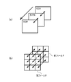
- FIG. 5 is a diagram conceptually showing motion detection in the entire field (FIG. 5A) and a diagram conceptually showing motion detection in a local region (FIG. 5B).
- FIG. 6A shows a conversion function between the first count value and the first value m1 (FIG. 6A), and FIG. 6B shows a conversion function between the second count value and the second value m2. is there.
- FIG. 1 is an external view of the electronic endoscope system 1 of the present embodiment.
- the electronic endoscope system 1 of the present embodiment includes an electronic scope 100 and a processor 200.
- the processor 200 is an apparatus that integrally includes a signal processing device that processes a signal from the electronic scope 100 and a light source device that irradiates a body cavity that does not reach natural light through the electronic scope 100.
- the signal processing device and the light source device may be configured separately.
- the electronic scope 100 includes an insertion portion flexible tube 11 covered with a flexible sheath.
- the distal end portion (bent portion 14) of the insertion portion flexible tube 11 bends in response to a remote operation from the hand operation portion 13 connected to the proximal end of the insertion portion flexible tube 11.
- the bending mechanism is a well-known mechanism incorporated in a general endoscope, and the bending portion 14 is bent by pulling the operation wire in conjunction with the rotation operation of the bending operation knob of the hand operation portion 13.
- the proximal end of the distal end portion 12 covered with a hard resin housing is connected to the distal end of the bent portion 14.
- the processor 200 is provided with a connector portion 20 having a connection structure corresponding to the connector portion 10 provided at the base end of the electronic scope 100.
- the connector unit 20 is mechanically connected to the connector unit 10 to electrically and optically connect the electronic scope 100 and the processor 200.
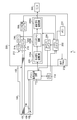
- FIG. 2 is a block diagram showing a configuration of the electronic endoscope system 1 of the present embodiment. As shown in FIG. 2, a monitor 300 is connected to a processor 200 in the electronic endoscope system 1.
- the processor 200 includes a system controller 202 and a timing controller 204.
- the system controller 202 performs overall control of the entire electronic endoscope system 1 by executing various programs stored in the memory 222. Further, the system controller 202 changes various settings of the electronic endoscope system 1 in accordance with instructions from the user (surgeon or assistant) input to the operation panel 218.
- the operation panel 218 has various configurations. As a specific configuration of the operation panel 218, for example, a hardware key for each function mounted on the front surface of the processor 200, a touch panel GUI (Graphical User Interface), a combination of a hardware key and a GUI, or the like can be considered.
- the timing controller 204 outputs a clock pulse for adjusting the operation timing of each unit to each circuit in the electronic endoscope system 1.
- the lamp 208 emits light (or light including at least the visible light region) having a spectrum that mainly extends from the visible light region to the invisible infrared light region after being started by the lamp power igniter 206.
- a high-intensity lamp such as a xenon lamp, a halogen lamp, or a metal halide lamp is suitable for the lamp 208. Irradiation light emitted from the lamp 208 is limited to an appropriate amount of light through the diaphragm 212 while being collected by the condenser lens 210.
- the motor 214 is mechanically connected to the diaphragm 212 via a transmission mechanism such as an arm or gear not shown.
- the motor 214 is a DC motor, for example, and is driven under the drive control of the driver 216.
- the aperture 212 is operated by the motor 214 to change the opening degree so that the image displayed on the display screen of the monitor 300 has an appropriate brightness.
- the amount of light emitted from the lamp 208 is limited according to the opening degree of the diaphragm 212.
- the appropriate reference for the brightness of the image is changed according to the brightness adjustment operation of the operation panel 218 by the operator.
- the dimming circuit that controls the brightness by controlling the driver 216 is a well-known circuit and is omitted in this specification.
- the irradiation light that has passed through the diaphragm 212 is incident on an incident end of an LCB (Light Carrying Bundle) 102.
- Irradiation light incident on the LCB 102 from the incident end propagates by repeating total reflection in the LCB 102.
- Irradiation light propagating through the LCB 102 is emitted from the exit end of the LCB 102 disposed in the distal end portion 12 of the electronic scope 100, and irradiates the subject via the light distribution lens 104.
- the solid-state image sensor 108 is an interlaced single-plate color CCD (Charge-Coupled Device) image sensor having a complementary color checkered pixel arrangement.
- the solid-state image sensor 108 accumulates an optical image formed by each pixel on the light receiving surface as a charge corresponding to the amount of light, and generates each of complementary colors signals of yellow Ye, cyan Cy, green G, and magenta Mg.
- the complementary color signals of two pixels adjacent in the vertical direction are added, mixed, and sequentially output.
- the solid-state image sensor 108 is not limited to a CCD image sensor, and may be a CMOS (Complementary Metal Oxide Semiconductor) image sensor or other types of imaging devices.
- the solid-state image sensor 108 may also be one equipped with a primary color filter (Bayer array filter).
- the imaging signal output from the solid-state imaging device 108 is input to the signal processing circuit 220 via the driver signal processing circuit 112 after signal amplification by the preamplifier 110.
- the electronic scope 100 includes a driver signal processing circuit 112 and a memory 114.
- the driver signal processing circuit 112 accesses the memory 114 and reads unique information of the electronic scope 100.
- Specific information of the electronic scope 100 recorded in the memory 114 includes, for example, the number of pixels and sensitivity of the solid-state imaging device 108, an operable field rate (frame rate), a model number, and the like.
- the driver signal processing circuit 112 outputs the unique information read from the memory 114 to the system controller 202.
- the system controller 202 performs various calculations based on the unique information of the electronic scope 100 and generates a control signal.
- the system controller 202 uses the generated control signal to control the operation and timing of various circuits in the processor 200 so that processing suitable for the electronic scope connected to the processor 200 is performed.
- the timing controller 204 supplies clock pulses to the driver signal processing circuit 112 and the signal processing circuit 220 according to the timing control by the system controller 202.
- the driver signal processing circuit 112 drives and controls the solid-state imaging device 108 at a timing synchronized with the field rate (frame rate) of the video processed on the processor 200 side in accordance with the clock pulse supplied from the timing controller 204.
- the signal processing circuit 220 includes a front-stage signal processing circuit 220A, a noise reduction circuit 220B, and a rear-stage signal processing circuit 220C.
- the pre-stage signal processing circuit 220A performs predetermined signal processing such as color complementation and Y / C separation on the image pickup signal input from the driver signal processing circuit 112 to obtain pixel signals (luminance signal Y, color difference signals U and V). And the generated pixel signal is output to the noise reduction circuit 220B.
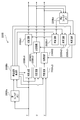
- FIG. 3 is a block diagram showing the configuration of the noise reduction circuit 220B.
- the noise reduction circuit 220B includes a first field memory 220Ba, a feedback coefficient calculation unit 220Bb, multiplication circuits 220Bc1 to 220Bc3, a second field memory 220Bd, multiplication circuits 220Be1 to 220Be3, and addition circuits 220Bf1 to 220Bf3. I have.
- the pixel signal (luminance signal Y) is input to the first field memory 220Ba from the previous stage signal processing circuit 220A.
- pixel signals for at least one field are buffered.
- the feedback coefficient calculation unit 220Bb sequentially receives the pixel signal (luminance signal Y) of the current field from the previous stage signal processing circuit 220A, and at the same time, the pixel of the previous field corresponding to the pixel signal from the first field memory 220Ba.
- a signal (luminance signal Y) is sequentially input.
- pixel signals of pixels of the same line and the same address are referred to as “corresponding pixel signals”.
- the pixel signal one field before corresponding to the pixel signal output first in the horizontal second line of the odd field is the pixel signal output first in the horizontal second line of the previous even field.
- FIG. 4 is a flowchart showing the operation of the feedback coefficient calculation unit 220Bb.
- FIG. 5A is a diagram conceptually illustrating motion detection in the entire field.
- this processing step S12 the following processing is performed in order to detect motion in the entire field as shown in FIG.
- this processing step S12 the pixels in the effective pixel area that have the luminance difference value calculated in the processing step S11 larger than the first threshold are counted. That is, in this processing step S12, since motion detection is performed for the entire field, pixels having a luminance difference value larger than the first threshold are counted for the two consecutive fields over the entire field.
- first count value the number of pixels counted in this processing step S12 is referred to as “first count value”.
- FIG. 6A is a graph showing the conversion function between the first count value and the first value m1.
- the vertical axis represents the first value m1
- the horizontal axis represents the first count value.
- the first value m1 takes a value of “0 to 9”.
- the first count value is converted to a constant value (here, “9”) when the value is equal to or less than a certain value C, and is converted to a smaller value as the value is larger than the certain value C. More specifically, when the first count value is larger than the constant value C, the first count value is converted to a smaller value with respect to “9”, and when the first count value becomes the maximum value (that is, the luminance difference value is increased in all pixels in the effective pixel region) When it is larger than the first threshold value), it is converted to “0”.
- a constant value here, “9”
- the first value m1 tends to be a small value when there are many moving areas of the subject in the entire field (there are many pixels whose luminance difference value is larger than the first threshold value), and the subject is within the entire field. Takes a large value when there are few moving regions (the number of pixels having a luminance difference value larger than the first threshold value is small). More simply, when the entire field is the detection range, the first value m1 takes a small value if the subject is moving, and takes a large value if the subject is not moving.
- a pixel group including the target pixel set in processing step S14 and its peripheral pixels is set.
- the peripheral pixels are a total of eight pixels located adjacent to each direction of the target pixel in the vertical and horizontal directions, diagonally upward to the right, diagonally downward to the right, diagonally upward to the left, and diagonally to the left. Point to. That is, the pixel group is composed of nine pixels arranged in a 3 ⁇ 3 matrix.
- FIG. 5B is a diagram conceptually illustrating motion detection in a local region (region composed of 3 ⁇ 3 pixels corresponding to a pixel group).
- this processing step S16 the following processing is performed in order to perform motion detection in the local region as shown in FIG.
- this processing step S16 a pixel group (one target pixel + 8 neighboring pixels) whose luminance difference value calculated in the processing step S11 is smaller than the second threshold is counted. That is, in this processing step S16, in order to perform motion detection in the local region, pixels having a luminance difference value smaller than the second threshold value for the two consecutive fields with the pixel group set in the processing step S15 as a range. Is counted.
- the number of pixels counted in this processing step S16 is referred to as a “second count value”.
- FIG. 6B is a graph showing the conversion function between the second count value and the second value m2.
- the vertical axis represents the second value m2
- the horizontal axis represents the second count value.
- the second value m2 takes a value of “0 to 9”.
- the second count value is converted into the number of pixels (values “0 to 9”) whose luminance difference value is smaller than the second threshold value. That is, the second value m1 is the same value as the second count value.
- the second value m2 takes a small value when there are many moving areas of the subject in the local area (there are many pixels whose luminance difference value is larger than the second threshold), and there are few moving areas of the subject within the local area. When the luminance difference value is smaller than the second threshold, there is a large value. More succinctly, when the local area is set as the detection range, the second value m2 takes a small value if the subject is moving, and takes a large value if the subject is not moving.
- This processing step S19 is performed when the difference value calculated in the processing step S18 is greater than or equal to the third threshold (S18: YES).
- the difference value calculated in the processing step S18 is typically greater than or equal to the third threshold in case 1 and case 2 below.
- Case 1 is a case where there are many regions where the subject moves in the entire field and there are few regions where the subject moves within the local region.
- the moving part of the subject is widely distributed in the field.
- the subject since the subject does not move so much when looking at the local area, it is detected that the subject is moving in the entire field. It is detected that the subject is not moving in the local region.
- Case 2 is a case where there are few areas where the subject moves in the entire field and there are many areas where the subject moves within the local area. In Case 2, for example, the subject does not move much when looking at the entire field, but the subject moves when looking at the local area, so it is detected that the subject is moving in the local area, It is detected that the subject is not moving.
- the difference value calculated in the processing step S18 is equal to or larger than the third threshold value, the result of the motion detection of the subject differs depending on whether it is viewed in the entire field or in the local area. For this reason, regarding the pixel signal of the target pixel belonging to the local region (pixel group), it is desirable to consider both the situation when the motion of the subject is observed in the entire field and the motion of the subject in the local region. Therefore, in this processing step S19, the feedback coefficient K applied to the pixel signal of the target pixel belonging to the local region (pixel group) is calculated by the following equation.
- This processing step S20 is performed when the difference value calculated in the processing step S18 is less than the third threshold (S18: NO).
- the difference value calculated in the processing step S18 is typically less than the third threshold in the case 3 and case 4 below.
- Case 3 is a case where there are few moving areas of the subject in the entire field and there are few moving areas of the subject even in the local area. In Case 3, for example, since the subject does not move so much not only in the entire field but also in a local region, it is detected that the subject does not move in any detection range.
- Case 4 is a case where there are many regions where the subject moves in the entire field, and there are many regions where the subject moves even within the local region. In Case 4, for example, moving subjects are widely distributed in the field, and the subject is moving even if a local region is seen. Therefore, it is detected that the subject is moving in any detection range.
- the difference value calculated in the processing step S18 is less than the third threshold value, the result of subject motion detection is the same when viewed in the entire field and when viewed in the local region. .
- the pixel signal of the pixel of interest belonging to the local region (pixel group) it is only necessary to consider one of the situation when the subject motion is observed in the entire field and the subject motion is viewed in the local region. Therefore, in this processing step S20, the feedback coefficient K applied to the pixel signal of the target pixel belonging to the local region (pixel group) is calculated by the following equation.
- the feedback coefficient K calculated by the feedback coefficient calculation unit 220Bb is input to the multiplication circuits 220Bc1 to 220Bc3 and the multiplication circuits 220Be1 to 220Be3.
- Each of the multiplication circuits 220Bc1 to 220Bc3 receives the current field pixel signal nfs (luminance signal Y), the current field pixel signal nfs (color difference signal U), and the current field pixel signal nfs (color difference signal V) from the previous stage signal processing circuit 220A. Is done.
- the current field pixel signal nfs (luminance signal Y), the current field pixel signal nfs (color difference signal U), and the current field pixel signal nfs (color difference signal V) input to the multiplication circuits 220Bc1 to 220Bc3 are respectively (1-feedback coefficient K). ).
- the multiplication values obtained by the multiplication circuits 220Bc1 to 220Bc3 are represented as “multiplication value (luminance signal Y) [nfs ⁇ (1-K)]” and “multiplication value (color difference signal U) [nfs ⁇ (1 ⁇ K)] ”,“ multiplication value (color difference signal V) [nfs ⁇ (1 ⁇ K)] ”.
- Multiplication value (luminance signal Y) [nfs ⁇ (1-K)]
- multiplication value (color difference signal U) [nfs ⁇ (1-K)]
- multiplication value (color difference signal V) [nfs ⁇ (1-K)]
- the corrected image signals (luminance signal Y and color difference signals U and V) output from the addition circuits 220Bf1 to 220Bf3 are input to the second field memory 220Bd.
- the corrected image signal is an image signal after noise reduction, which will be described in detail later.
- pixel signals for at least one field are buffered.
- the multiplication circuits 220Be1 to 220Be3 respectively receive the previous field pixel signal pfs (corrected luminance signal Y), the previous field pixel signal pfs (corrected color difference signal U), and the previous field pixel signal pfs (from the second field memory 220Bd.
- the corrected color difference signal V) is input.
- Previous field pixel signal pfs corrected luminance signal Y
- previous field pixel signal pfs corrected color difference signal U
- previous field pixel signal pfs corrected color difference signal V
- the multiplication values obtained by the multiplication circuits 220Be1 to 220Be3 are represented by “multiplication value (luminance signal Y) [pfs ⁇ K]”, “multiplication value (color difference signal U) [pfs ⁇ K]”, and “multiplication value”, respectively.
- the multiplication value (luminance signal Y) [pfs ⁇ K], the multiplication value (color difference signal U) [pfs ⁇ K], and the multiplication value (color difference signal V) [pfs ⁇ K] are input to the addition circuits 220Bf1 to 220Bf3, respectively. .
- the addition circuit 220Bf1 has a multiplication value (luminance signal Y) [nfs ⁇ (1-K)] input from the multiplication circuit 220Bc1 and a multiplication value (luminance signal Y) [pfs ⁇ K] input from the multiplication circuit 220Be1.
- the adder circuit 220Bf2 has a multiplication value (color difference signal U) [nfs ⁇ (1-K)] input from the multiplication circuit 220Bc2 and a multiplication value (color difference signal U) [pfs ⁇ K] input from the multiplication circuit 220Be2.
- RGB luminance signal
- the adder circuit 220Bf3 has a multiplication value (color difference signal V) [nfs ⁇ (1-K)] input from the multiplication circuit 220Bc3 and a multiplication value (color difference signal V) [pfs ⁇ K] input from the multiplication circuit 220Be3. Are output to the post-stage signal processing circuit 220C.
- the addition circuits Bf1 to Bf3 correct the current field pixel signal nfs by mixing the current field pixel signal nfs and the previous field pixel signal pfs according to the following equation.
- the mixing ratio between the current field pixel signal nfs and the previous field pixel signal pfs is determined according to the feedback coefficient K.
- the feedback coefficient K decreases as the subject moves, and increases as the subject does not move. Since the ratio of the current field pixel signal nfs becomes higher as the feedback coefficient K is closer to 0, the afterimage is suppressed instead of reducing the noise reduction effect in the pixel. Further, since the ratio of the previous field pixel signal pfs becomes higher as the feedback coefficient K is closer to 1, the noise reduction effect in the pixel becomes higher.
- the post-stage signal processing circuit 220C converts the corrected current field pixel signal nfs ′ (luminance signal Y, chrominance signals U, V) input from the addition circuits 220Bf1 to 220Bf3 into NTSC (National Television System Committee) or PAL (Phase Alternating Line). ) And the like, and the converted video signal is output to the monitor 300. By sequentially inputting video signals to the monitor 300, a color image of the subject is displayed on the display screen of the monitor 300.
- NTSC National Television System Committee
- PAL Phase Alternating Line
- Embodiments of the present invention are not limited to those described above, and various modifications are possible within the scope of the technical idea of the present invention.
- the embodiment of the present application also includes an embodiment that is exemplarily specified in the specification or a combination of obvious embodiments and the like as appropriate.
- the imaging period of the solid-state imaging device 108 is a field period, but in another embodiment, it may be a frame period.
Landscapes
- Engineering & Computer Science (AREA)
- Multimedia (AREA)
- Signal Processing (AREA)
- Physics & Mathematics (AREA)
- General Physics & Mathematics (AREA)
- Theoretical Computer Science (AREA)
- Computer Vision & Pattern Recognition (AREA)
- Studio Devices (AREA)
- Endoscopes (AREA)
- Picture Signal Circuits (AREA)
- Transforming Light Signals Into Electric Signals (AREA)
Abstract
Description
図4は、帰還係数算出部220Bbの動作を示すフローチャートである。
図4に示されるように、本処理ステップS11では、有効画素領域内の各画素について、現在のフィールドの画素信号(輝度信号Y)と1つ前のフィールドの画素信号(輝度信号Y)との差分値が計算される。以下、説明の便宜上、本処理ステップS11にて計算される画素信号(輝度信号Y)の差分値を「輝度差分値」と記す。また、現在のフィールドの画素信号(輝度信号Y、色差信号U、V)を「現フィールド画素信号nfs」と記し、1つ前のフィールドの画素信号(輝度信号Y、色差信号U、V)を「前フィールド画素信号pfs」と記す。
図5(a)は、フィールド全体での動き検出を概念的に示す図である。本処理ステップS12では、図5(a)に示されるようにフィールド全体での動き検出を行うため、以下の処理が行われる。
本処理ステップS13では、処理ステップS12にてカウントされた第1カウント値を第1の値m1に変換する。ここで、図6(a)に、第1カウント値と第1の値m1との変換関数をグラフ化して示す。図6(a)中、縦軸は、第1の値m1を示し、横軸は、第1カウント値を示す。第1の値m1は、「0~9」の値をとる。
本処理ステップS14では、有効画素領域内の一つの画素が注目画素として設定される。
本処理ステップS15では、処理ステップS14にて設定された注目画素及びその周辺画素よりなる画素群を設定する。なお、本実施形態において、周辺画素は、注目画素の上下左右方向、右斜め上方向、右斜め下方向、左斜め上方向及び左斜め下方向の各方向に隣接して位置する計8つの画素を指す。すなわち、画素群は、3×3のマトリクスに配置された9つの画素よりなる。
図5(b)は、局所領域(画素群に対応する3×3の画素よりなる領域)での動き検出を概念的に示す図である。本処理ステップS16では、図5(b)に示されるように局所領域での動き検出を行うため、以下の処理が行われる。
本処理ステップS17では、処理ステップS16にてカウントされた第2カウント値を第2の値m2に変換する。ここで、図6(b)に、第2カウント値と第2の値m2との変換関数をグラフ化して示す。図6(b)中、縦軸は、第2の値m2を示し、横軸は、第2カウント値を示す。第2の値m2も第1の値m1と同じく「0~9」の値をとる。
本処理ステップS18では、第1の値m1と第2の値m2との差分値が計算される。次いで、計算された差分値が第3の閾値以上であるか否かが判定される。
本処理ステップS19は、処理ステップS18にて計算された差分値が第3の閾値以上となる場合(S18:YES)に行われる。処理ステップS18にて計算される差分値は、典型的には、下記のケース1やケース2の場合に第3の閾値以上となる。
ケース1は、フィールド全体の中で被写体の動く領域が多く且つ局所領域内で被写体の動く領域が少ないケースである。ケース1では、例えば、被写体の動いている部分がフィールド内で広く分布するが、局所的な領域を見ると被写体があまり動いていないため、フィールド全体では被写体が動いていると検出されるが、局所領域では被写体が動いていないと検出される。
ケース2は、フィールド全体の中で被写体の動く領域が少なく且つ局所領域内で被写体の動く領域が多いケースである。ケース2では、例えば、フィールド全体を見ると被写体があまり動いていないが、局所的な領域を見ると被写体が動いているため、局所領域では被写体が動いていると検出されるが、フィールド全体では被写体が動いていないと検出される。
本処理ステップS20は、処理ステップS18にて計算された差分値が第3の閾値未満となる場合(S18:NO)に行われる。処理ステップS18にて計算される差分値は、典型的には、下記のケース3やケース4の場合に第3の閾値未満となる。
ケース3は、フィールド全体の中で被写体の動く領域が少なく且つ局所領域内でも被写体の動く領域が少ないケースである。ケース3では、例えば、フィールド全体だけでなく局所的な領域を見ても被写体があまり動いていないため、何れの検出範囲でも被写体が動いていないと検出される。
ケース4は、フィールド全体の中で被写体の動く領域が多く且つ局所領域内でも被写体の動く領域が多いケースである。ケース4では、例えば、動いている被写体がフィールド内で広く分布し、局所的な領域を見ても被写体が動いているため、何れも検出範囲でも被写体が動いていると検出される。
本処理ステップS21では、有効画素領域内において、適用する帰還係数Kが算出されていない画素が残っているか否かが判定される。適用する帰還係数Kが算出されていない画素が残っている場合(S21:YES)、注目画素が次の画素(例えば水平ライン方向に隣接する画素)に設定される(S22)。次の注目画素が設定されると、本フローチャートは、処理ステップS15に戻る。処理ステップS15~S22がループすることで、有効画素領域内の各画素について帰還係数Kが順次算出される。本フローチャートは、有効画素領域内の全ての画素について帰還係数Kが算出されると(S21:NO)、上記ループから抜けて終了する。
Claims (6)
- 被写体を所定の撮像期間で周期的に撮像する撮像素子の有効画素領域内の各画素について、該撮像素子より出力される現在の撮像期間の画素信号と1つ前の撮像期間の画素信号との差分値を計算する差分値計算手段と、
前記有効画素領域全てを範囲として前記被写体の動きを検出する第1の動き検出手段と、
前記有効画素領域内の各画素を注目画素として順次設定する注目画素設定手段と、
順次設定される注目画素を含む局所画素領域を範囲として前記被写体の動きを検出する第2の動き検出手段と、
各前記注目画素について、前記第1の動き検出手段による検出結果及び前記第2の動き検出手段による検出結果に基づき、現在の撮像期間の画素信号と1つ前の撮像期間の画素信号との混合比を決定する混合比決定手段と、
前記各注目画素について、前記混合比決定手段により決定された混合比に基づいて現在の撮像期間の画素信号を補正する画素信号補正手段と、
を備える、
画像処理装置。 - 被写体を所定の撮像期間で周期的に撮像する撮像素子の有効画素領域内の各画素について、該撮像素子より出力される現在の撮像期間の画素信号と1つ前の撮像期間の画素信号との差分値を計算する差分値計算手段と、
前記有効画素領域内において前記差分値が第1の条件を満たす画素をカウントし、カウントされた画素の数を第1カウント値とする第1のカウント手段と、
前記有効画素領域内の各画素を注目画素として順次設定する注目画素設定手段と、
順次設定される注目画素及びその周辺画素よりなる画素群の中で前記差分値が第2の条件を満たすものをカウントし、カウントされた画素の数を第2カウント値とする第2のカウント手段と、
各前記注目画素について、当該注目画素が属する画素群における第2カウント値と前記第1カウント値に基づいて現在の撮像期間の画素信号と1つ前の撮像期間の画素信号との混合比を決定する混合比決定手段と、
前記各注目画素について、前記混合比決定手段により決定された混合比に基づいて現在の撮像期間の画素信号を補正する画素信号補正手段と、
を備える、
画像処理装置。 - 前記混合比決定手段は、
前記第1カウント値を第1の値に変換し、
前記第2カウント値を第2の値に変換し、
前記第1の値と前記第2の値との差分値に基づいて現在の撮像期間の画素信号と1つ前の撮像期間の画素信号との混合比を決定する、
請求項2に記載の画像処理装置。 - 前記第1の値の数値範囲と前記第2の値の数値範囲は同一である、
請求項3に記載の画像処理装置。 - 前記第1の条件は、
前記差分値が第1の閾値よりも大きいことであり、
前記第2の条件は、
前記差分値が第2の閾値よりも小さいことであり、
前記第1カウント値は、
一定値以下のときには前記数値範囲内の最大値に変換され、
前記一定値より大きいほど前記最大値に対して小さい値に変換され、
前記第2カウント値は、
前記第2カウント値そのままの値に変換され、
前記混合比決定手段は、
前記第1の値と前記第2の値との差分値が第3の閾値以上のときには該第1の値及び該第2の値に基づいて前記混合比を決定し、
前記第1の値と前記第2の値との差分値が第3の閾値未満のときには該第1の値又は該第2の値に基づいて前記混合比を決定する、
請求項4に記載の画像処理装置。 - 前記撮像期間は、
1フィールド期間又は1フレーム期間である、
請求項1から請求項5の何れか一項に記載の画像処理装置。
Priority Applications (6)
| Application Number | Priority Date | Filing Date | Title |
|---|---|---|---|
| KR1020167015786A KR101809476B1 (ko) | 2014-04-11 | 2015-03-26 | 화상 처리 장치 |
| EP15776531.4A EP3131286B1 (en) | 2014-04-11 | 2015-03-26 | Image processing device |
| US15/037,808 US9842383B2 (en) | 2014-04-11 | 2015-03-26 | Image processing device |
| CA2931074A CA2931074C (en) | 2014-04-11 | 2015-03-26 | Electronic endoscope system |
| AU2015244984A AU2015244984B2 (en) | 2014-04-11 | 2015-03-26 | Electronic Endoscope System |
| CN201580003142.6A CN105830433B (zh) | 2014-04-11 | 2015-03-26 | 图像处理设备 |
Applications Claiming Priority (2)
| Application Number | Priority Date | Filing Date | Title |
|---|---|---|---|
| JP2014-081918 | 2014-04-11 | ||
| JP2014081918A JP6411768B2 (ja) | 2014-04-11 | 2014-04-11 | 画像処理装置 |
Publications (1)
| Publication Number | Publication Date |
|---|---|
| WO2015156142A1 true WO2015156142A1 (ja) | 2015-10-15 |
Family
ID=54287719
Family Applications (1)
| Application Number | Title | Priority Date | Filing Date |
|---|---|---|---|
| PCT/JP2015/059360 Ceased WO2015156142A1 (ja) | 2014-04-11 | 2015-03-26 | 画像処理装置 |
Country Status (8)
| Country | Link |
|---|---|
| US (1) | US9842383B2 (ja) |
| EP (1) | EP3131286B1 (ja) |
| JP (1) | JP6411768B2 (ja) |
| KR (1) | KR101809476B1 (ja) |
| CN (1) | CN105830433B (ja) |
| AU (1) | AU2015244984B2 (ja) |
| CA (1) | CA2931074C (ja) |
| WO (1) | WO2015156142A1 (ja) |
Families Citing this family (2)
| Publication number | Priority date | Publication date | Assignee | Title |
|---|---|---|---|---|
| CN109151348B (zh) * | 2018-09-28 | 2021-01-08 | 维沃移动通信有限公司 | 一种图像处理方法、电子设备及计算机可读存储介质 |
| WO2020170369A1 (ja) * | 2019-02-20 | 2020-08-27 | オリンパス株式会社 | 情報処理装置、情報処理システム、情報処理方法およびプログラム |
Citations (3)
| Publication number | Priority date | Publication date | Assignee | Title |
|---|---|---|---|---|
| JP2000209507A (ja) * | 1999-01-12 | 2000-07-28 | Toshiba Corp | 固体撮像装置の低ノイズ化回路 |
| JP2012019426A (ja) * | 2010-07-09 | 2012-01-26 | Hoya Corp | ノイズ除去装置 |
| JP2012129913A (ja) * | 2010-12-17 | 2012-07-05 | Sanyo Electric Co Ltd | ノイズ低減装置 |
Family Cites Families (19)
| Publication number | Priority date | Publication date | Assignee | Title |
|---|---|---|---|---|
| DE68909271T2 (de) * | 1988-02-23 | 1994-03-24 | Philips Nv | Verfahren und Anordnung zum Abschätzen des Bewegungsausmasses bei einem Bildelement eines Fernsehbildes. |
| JP2934036B2 (ja) * | 1991-03-07 | 1999-08-16 | 松下電器産業株式会社 | 動き検出方法およびノイズ低減装置 |
| JP3660731B2 (ja) | 1995-11-13 | 2005-06-15 | ペンタックス株式会社 | 電子内視鏡 |
| WO1998018256A2 (en) * | 1996-10-24 | 1998-04-30 | Philips Electronics N.V. | Noise filtering |
| US6130707A (en) * | 1997-04-14 | 2000-10-10 | Philips Electronics N.A. Corp. | Video motion detector with global insensitivity |
| US6847408B1 (en) * | 2000-07-27 | 2005-01-25 | Richard W. Webb | Method and apparatus for reducing noise in an image sequence |
| US7724307B2 (en) * | 2004-07-28 | 2010-05-25 | Broadcom Corporation | Method and system for noise reduction in digital video |
| CN100486299C (zh) | 2004-12-21 | 2009-05-06 | 索尼株式会社 | 图像处理装置和图像处理方法 |
| JP5052319B2 (ja) * | 2007-12-17 | 2012-10-17 | オリンパス株式会社 | 動画ノイズ低減処理装置、動画ノイズ低減処理プログラム、動画ノイズ低減処理方法 |
| JP2009290827A (ja) * | 2008-06-02 | 2009-12-10 | Sony Corp | 画像処理装置および画像処理方法 |
| CN101859440A (zh) * | 2010-05-31 | 2010-10-13 | 浙江捷尚视觉科技有限公司 | 基于块的运动区域检测方法 |
| CN101894378B (zh) * | 2010-06-13 | 2012-09-05 | 南京航空航天大学 | 基于双感兴趣区域的运动目标视觉跟踪方法及系统 |
| JP5645636B2 (ja) * | 2010-12-16 | 2014-12-24 | 三菱電機株式会社 | フレーム補間装置及び方法 |
| JP2012142829A (ja) * | 2011-01-05 | 2012-07-26 | Sony Corp | 画像処理装置および画像処理方法 |
| JP2012257193A (ja) | 2011-05-13 | 2012-12-27 | Sony Corp | 画像処理装置、撮像装置、および画像処理方法、並びにプログラム |
| TWI459325B (zh) | 2011-05-13 | 2014-11-01 | Altek Corp | 數位影像處理裝置及其處理方法 |
| JP2013074571A (ja) | 2011-09-29 | 2013-04-22 | Sony Corp | 画像処理装置および方法、プログラム、並びに記録媒体 |
| JPWO2014091943A1 (ja) * | 2012-12-14 | 2017-01-05 | ソニー株式会社 | 画像処理装置および方法 |
| KR101652658B1 (ko) * | 2014-02-07 | 2016-08-30 | 가부시키가이샤 모르포 | 화상 처리 장치, 화상 처리 방법, 화상 처리 프로그램 및 기록 매체 |
-
2014
- 2014-04-11 JP JP2014081918A patent/JP6411768B2/ja active Active
-
2015
- 2015-03-26 WO PCT/JP2015/059360 patent/WO2015156142A1/ja not_active Ceased
- 2015-03-26 AU AU2015244984A patent/AU2015244984B2/en active Active
- 2015-03-26 CA CA2931074A patent/CA2931074C/en active Active
- 2015-03-26 KR KR1020167015786A patent/KR101809476B1/ko active Active
- 2015-03-26 CN CN201580003142.6A patent/CN105830433B/zh active Active
- 2015-03-26 US US15/037,808 patent/US9842383B2/en active Active
- 2015-03-26 EP EP15776531.4A patent/EP3131286B1/en active Active
Patent Citations (3)
| Publication number | Priority date | Publication date | Assignee | Title |
|---|---|---|---|---|
| JP2000209507A (ja) * | 1999-01-12 | 2000-07-28 | Toshiba Corp | 固体撮像装置の低ノイズ化回路 |
| JP2012019426A (ja) * | 2010-07-09 | 2012-01-26 | Hoya Corp | ノイズ除去装置 |
| JP2012129913A (ja) * | 2010-12-17 | 2012-07-05 | Sanyo Electric Co Ltd | ノイズ低減装置 |
Non-Patent Citations (1)
| Title |
|---|
| See also references of EP3131286A4 * |
Also Published As
| Publication number | Publication date |
|---|---|
| CN105830433A (zh) | 2016-08-03 |
| KR20160085340A (ko) | 2016-07-15 |
| EP3131286A4 (en) | 2017-11-01 |
| EP3131286B1 (en) | 2020-12-23 |
| US20160292828A1 (en) | 2016-10-06 |
| AU2015244984B2 (en) | 2018-01-18 |
| CN105830433B (zh) | 2017-12-05 |
| CA2931074A1 (en) | 2015-10-15 |
| KR101809476B1 (ko) | 2017-12-15 |
| JP2015204486A (ja) | 2015-11-16 |
| EP3131286A1 (en) | 2017-02-15 |
| JP6411768B2 (ja) | 2018-10-24 |
| CA2931074C (en) | 2018-04-03 |
| US9842383B2 (en) | 2017-12-12 |
| AU2015244984A1 (en) | 2016-06-09 |
Similar Documents
| Publication | Publication Date | Title |
|---|---|---|
| JP2013066168A (ja) | 撮像素子、及び撮像装置 | |
| US10027919B2 (en) | Signal processing apparatus, image capturing apparatus, control apparatus, signal processing method, and control method | |
| JP5708036B2 (ja) | 撮像装置 | |
| JP6411768B2 (ja) | 画像処理装置 | |
| JP6099009B2 (ja) | 撮像素子および撮像装置 | |
| US11160443B2 (en) | Electronic endoscope device for changing observation image brightness | |
| JP2010068020A (ja) | 画像入力装置 | |
| WO2018008009A1 (ja) | 画像処理装置及び電子内視鏡システム | |
| JP2011176671A (ja) | 撮像システム | |
| JP2011156214A (ja) | 撮像装置、及び電子内視鏡システム | |
| JP6535435B2 (ja) | プロセッサ及び内視鏡システム | |
| JP6272115B2 (ja) | 内視鏡プロセッサおよび内視鏡システム | |
| JP2011211497A (ja) | 画像入力装置 | |
| JP6650969B2 (ja) | 内視鏡システム | |
| JP6370604B2 (ja) | 内視鏡システム | |
| US10158792B2 (en) | Method for displaying image, image pickup system and endoscope apparatus including the same | |
| US12022992B2 (en) | Image signal processing device, image signal processing method, and program | |
| KR20150088645A (ko) | 촬영 장치, 그 제어 방법, 및 컴퓨터 판독가능 기록매체 | |
| JP3917982B2 (ja) | 内視鏡装置 | |
| JP2010279507A (ja) | 電子内視鏡システム | |
| JP6491736B2 (ja) | 内視鏡プロセッサおよび内視鏡システム | |
| JP6741412B2 (ja) | 信号伝送装置及び電子内視鏡システム | |
| JP2011172783A (ja) | 画像処理装置、及び電子内視鏡システム | |
| KR101722479B1 (ko) | 카메라의 백라이트 보정 장치 및 방법 | |
| JP2004267580A (ja) | 電子内視鏡装置 |
Legal Events
| Date | Code | Title | Description |
|---|---|---|---|
| 121 | Ep: the epo has been informed by wipo that ep was designated in this application |
Ref document number: 15776531 Country of ref document: EP Kind code of ref document: A1 |
|
| ENP | Entry into the national phase |
Ref document number: 2931074 Country of ref document: CA |
|
| WWE | Wipo information: entry into national phase |
Ref document number: 15037808 Country of ref document: US |
|
| REEP | Request for entry into the european phase |
Ref document number: 2015776531 Country of ref document: EP |
|
| WWE | Wipo information: entry into national phase |
Ref document number: 2015776531 Country of ref document: EP |
|
| ENP | Entry into the national phase |
Ref document number: 2015244984 Country of ref document: AU Date of ref document: 20150326 Kind code of ref document: A |
|
| ENP | Entry into the national phase |
Ref document number: 20167015786 Country of ref document: KR Kind code of ref document: A |
|
| NENP | Non-entry into the national phase |
Ref country code: DE |