WO2015163109A1 - 波長変換部材およびその製造方法 - Google Patents
波長変換部材およびその製造方法 Download PDFInfo
- Publication number
- WO2015163109A1 WO2015163109A1 PCT/JP2015/060517 JP2015060517W WO2015163109A1 WO 2015163109 A1 WO2015163109 A1 WO 2015163109A1 JP 2015060517 W JP2015060517 W JP 2015060517W WO 2015163109 A1 WO2015163109 A1 WO 2015163109A1
- Authority
- WO
- WIPO (PCT)
- Prior art keywords
- phosphor ceramic
- wavelength conversion
- layer
- phosphor
- conversion member
- Prior art date
- Legal status (The legal status is an assumption and is not a legal conclusion. Google has not performed a legal analysis and makes no representation as to the accuracy of the status listed.)
- Ceased
Links
Images


Classifications
-
- H—ELECTRICITY
- H10—SEMICONDUCTOR DEVICES; ELECTRIC SOLID-STATE DEVICES NOT OTHERWISE PROVIDED FOR
- H10H—INORGANIC LIGHT-EMITTING SEMICONDUCTOR DEVICES HAVING POTENTIAL BARRIERS
- H10H20/00—Individual inorganic light-emitting semiconductor devices having potential barriers, e.g. light-emitting diodes [LED]
- H10H20/80—Constructional details
- H10H20/85—Packages
- H10H20/851—Wavelength conversion means
- H10H20/8511—Wavelength conversion means characterised by their material, e.g. binder
- H10H20/8512—Wavelength conversion materials
-
- C—CHEMISTRY; METALLURGY
- C04—CEMENTS; CONCRETE; ARTIFICIAL STONE; CERAMICS; REFRACTORIES
- C04B—LIME, MAGNESIA; SLAG; CEMENTS; COMPOSITIONS THEREOF, e.g. MORTARS, CONCRETE OR LIKE BUILDING MATERIALS; ARTIFICIAL STONE; CERAMICS; REFRACTORIES; TREATMENT OF NATURAL STONE
- C04B35/00—Shaped ceramic products characterised by their composition; Ceramics compositions; Processing powders of inorganic compounds preparatory to the manufacturing of ceramic products
- C04B35/50—Shaped ceramic products characterised by their composition; Ceramics compositions; Processing powders of inorganic compounds preparatory to the manufacturing of ceramic products based on rare-earth compounds
-
- C—CHEMISTRY; METALLURGY
- C04—CEMENTS; CONCRETE; ARTIFICIAL STONE; CERAMICS; REFRACTORIES
- C04B—LIME, MAGNESIA; SLAG; CEMENTS; COMPOSITIONS THEREOF, e.g. MORTARS, CONCRETE OR LIKE BUILDING MATERIALS; ARTIFICIAL STONE; CERAMICS; REFRACTORIES; TREATMENT OF NATURAL STONE
- C04B35/00—Shaped ceramic products characterised by their composition; Ceramics compositions; Processing powders of inorganic compounds preparatory to the manufacturing of ceramic products
- C04B35/50—Shaped ceramic products characterised by their composition; Ceramics compositions; Processing powders of inorganic compounds preparatory to the manufacturing of ceramic products based on rare-earth compounds
- C04B35/505—Shaped ceramic products characterised by their composition; Ceramics compositions; Processing powders of inorganic compounds preparatory to the manufacturing of ceramic products based on rare-earth compounds based on yttrium oxide
-
- C—CHEMISTRY; METALLURGY
- C04—CEMENTS; CONCRETE; ARTIFICIAL STONE; CERAMICS; REFRACTORIES
- C04B—LIME, MAGNESIA; SLAG; CEMENTS; COMPOSITIONS THEREOF, e.g. MORTARS, CONCRETE OR LIKE BUILDING MATERIALS; ARTIFICIAL STONE; CERAMICS; REFRACTORIES; TREATMENT OF NATURAL STONE
- C04B35/00—Shaped ceramic products characterised by their composition; Ceramics compositions; Processing powders of inorganic compounds preparatory to the manufacturing of ceramic products
- C04B35/622—Forming processes; Processing powders of inorganic compounds preparatory to the manufacturing of ceramic products
-
- C—CHEMISTRY; METALLURGY
- C04—CEMENTS; CONCRETE; ARTIFICIAL STONE; CERAMICS; REFRACTORIES
- C04B—LIME, MAGNESIA; SLAG; CEMENTS; COMPOSITIONS THEREOF, e.g. MORTARS, CONCRETE OR LIKE BUILDING MATERIALS; ARTIFICIAL STONE; CERAMICS; REFRACTORIES; TREATMENT OF NATURAL STONE
- C04B35/00—Shaped ceramic products characterised by their composition; Ceramics compositions; Processing powders of inorganic compounds preparatory to the manufacturing of ceramic products
- C04B35/622—Forming processes; Processing powders of inorganic compounds preparatory to the manufacturing of ceramic products
- C04B35/62218—Forming processes; Processing powders of inorganic compounds preparatory to the manufacturing of ceramic products obtaining ceramic films, e.g. by using temporary supports
-
- C—CHEMISTRY; METALLURGY
- C04—CEMENTS; CONCRETE; ARTIFICIAL STONE; CERAMICS; REFRACTORIES
- C04B—LIME, MAGNESIA; SLAG; CEMENTS; COMPOSITIONS THEREOF, e.g. MORTARS, CONCRETE OR LIKE BUILDING MATERIALS; ARTIFICIAL STONE; CERAMICS; REFRACTORIES; TREATMENT OF NATURAL STONE
- C04B35/00—Shaped ceramic products characterised by their composition; Ceramics compositions; Processing powders of inorganic compounds preparatory to the manufacturing of ceramic products
- C04B35/622—Forming processes; Processing powders of inorganic compounds preparatory to the manufacturing of ceramic products
- C04B35/626—Preparing or treating the powders individually or as batches ; preparing or treating macroscopic reinforcing agents for ceramic products, e.g. fibres; mechanical aspects section B
- C04B35/63—Preparing or treating the powders individually or as batches ; preparing or treating macroscopic reinforcing agents for ceramic products, e.g. fibres; mechanical aspects section B using additives specially adapted for forming the products, e.g.. binder binders
- C04B35/632—Organic additives
- C04B35/634—Polymers
-
- C—CHEMISTRY; METALLURGY
- C04—CEMENTS; CONCRETE; ARTIFICIAL STONE; CERAMICS; REFRACTORIES
- C04B—LIME, MAGNESIA; SLAG; CEMENTS; COMPOSITIONS THEREOF, e.g. MORTARS, CONCRETE OR LIKE BUILDING MATERIALS; ARTIFICIAL STONE; CERAMICS; REFRACTORIES; TREATMENT OF NATURAL STONE
- C04B35/00—Shaped ceramic products characterised by their composition; Ceramics compositions; Processing powders of inorganic compounds preparatory to the manufacturing of ceramic products
- C04B35/622—Forming processes; Processing powders of inorganic compounds preparatory to the manufacturing of ceramic products
- C04B35/626—Preparing or treating the powders individually or as batches ; preparing or treating macroscopic reinforcing agents for ceramic products, e.g. fibres; mechanical aspects section B
- C04B35/63—Preparing or treating the powders individually or as batches ; preparing or treating macroscopic reinforcing agents for ceramic products, e.g. fibres; mechanical aspects section B using additives specially adapted for forming the products, e.g.. binder binders
- C04B35/638—Removal thereof
-
- C—CHEMISTRY; METALLURGY
- C04—CEMENTS; CONCRETE; ARTIFICIAL STONE; CERAMICS; REFRACTORIES
- C04B—LIME, MAGNESIA; SLAG; CEMENTS; COMPOSITIONS THEREOF, e.g. MORTARS, CONCRETE OR LIKE BUILDING MATERIALS; ARTIFICIAL STONE; CERAMICS; REFRACTORIES; TREATMENT OF NATURAL STONE
- C04B35/00—Shaped ceramic products characterised by their composition; Ceramics compositions; Processing powders of inorganic compounds preparatory to the manufacturing of ceramic products
- C04B35/622—Forming processes; Processing powders of inorganic compounds preparatory to the manufacturing of ceramic products
- C04B35/64—Burning or sintering processes
-
- C—CHEMISTRY; METALLURGY
- C04—CEMENTS; CONCRETE; ARTIFICIAL STONE; CERAMICS; REFRACTORIES
- C04B—LIME, MAGNESIA; SLAG; CEMENTS; COMPOSITIONS THEREOF, e.g. MORTARS, CONCRETE OR LIKE BUILDING MATERIALS; ARTIFICIAL STONE; CERAMICS; REFRACTORIES; TREATMENT OF NATURAL STONE
- C04B41/00—After-treatment of mortars, concrete, artificial stone or ceramics; Treatment of natural stone
- C04B41/80—After-treatment of mortars, concrete, artificial stone or ceramics; Treatment of natural stone of only ceramics
- C04B41/81—Coating or impregnation
- C04B41/85—Coating or impregnation with inorganic materials
- C04B41/87—Ceramics
-
- C—CHEMISTRY; METALLURGY
- C09—DYES; PAINTS; POLISHES; NATURAL RESINS; ADHESIVES; COMPOSITIONS NOT OTHERWISE PROVIDED FOR; APPLICATIONS OF MATERIALS NOT OTHERWISE PROVIDED FOR
- C09K—MATERIALS FOR MISCELLANEOUS APPLICATIONS, NOT PROVIDED FOR ELSEWHERE
- C09K11/00—Luminescent materials, e.g. electroluminescent or chemiluminescent
- C09K11/08—Luminescent materials, e.g. electroluminescent or chemiluminescent containing inorganic luminescent materials
- C09K11/77—Luminescent materials, e.g. electroluminescent or chemiluminescent containing inorganic luminescent materials containing rare earth metals
- C09K11/7766—Luminescent materials, e.g. electroluminescent or chemiluminescent containing inorganic luminescent materials containing rare earth metals containing two or more rare earth metals
- C09K11/7774—Aluminates
-
- F—MECHANICAL ENGINEERING; LIGHTING; HEATING; WEAPONS; BLASTING
- F21—LIGHTING
- F21K—NON-ELECTRIC LIGHT SOURCES USING LUMINESCENCE; LIGHT SOURCES USING ELECTROCHEMILUMINESCENCE; LIGHT SOURCES USING CHARGES OF COMBUSTIBLE MATERIAL; LIGHT SOURCES USING SEMICONDUCTOR DEVICES AS LIGHT-GENERATING ELEMENTS; LIGHT SOURCES NOT OTHERWISE PROVIDED FOR
- F21K9/00—Light sources using semiconductor devices as light-generating elements, e.g. using light-emitting diodes [LED] or lasers
- F21K9/60—Optical arrangements integrated in the light source, e.g. for improving the colour rendering index or the light extraction
- F21K9/64—Optical arrangements integrated in the light source, e.g. for improving the colour rendering index or the light extraction using wavelength conversion means distinct or spaced from the light-generating element, e.g. a remote phosphor layer
-
- F—MECHANICAL ENGINEERING; LIGHTING; HEATING; WEAPONS; BLASTING
- F21—LIGHTING
- F21V—FUNCTIONAL FEATURES OR DETAILS OF LIGHTING DEVICES OR SYSTEMS THEREOF; STRUCTURAL COMBINATIONS OF LIGHTING DEVICES WITH OTHER ARTICLES, NOT OTHERWISE PROVIDED FOR
- F21V29/00—Protecting lighting devices from thermal damage; Cooling or heating arrangements specially adapted for lighting devices or systems
- F21V29/50—Cooling arrangements
- F21V29/70—Cooling arrangements characterised by passive heat-dissipating elements, e.g. heat-sinks
- F21V29/74—Cooling arrangements characterised by passive heat-dissipating elements, e.g. heat-sinks with fins or blades
- F21V29/76—Cooling arrangements characterised by passive heat-dissipating elements, e.g. heat-sinks with fins or blades with essentially identical parallel planar fins or blades, e.g. with comb-like cross-section
-
- H—ELECTRICITY
- H10—SEMICONDUCTOR DEVICES; ELECTRIC SOLID-STATE DEVICES NOT OTHERWISE PROVIDED FOR
- H10H—INORGANIC LIGHT-EMITTING SEMICONDUCTOR DEVICES HAVING POTENTIAL BARRIERS
- H10H20/00—Individual inorganic light-emitting semiconductor devices having potential barriers, e.g. light-emitting diodes [LED]
- H10H20/01—Manufacture or treatment
-
- H—ELECTRICITY
- H10—SEMICONDUCTOR DEVICES; ELECTRIC SOLID-STATE DEVICES NOT OTHERWISE PROVIDED FOR
- H10H—INORGANIC LIGHT-EMITTING SEMICONDUCTOR DEVICES HAVING POTENTIAL BARRIERS
- H10H20/00—Individual inorganic light-emitting semiconductor devices having potential barriers, e.g. light-emitting diodes [LED]
- H10H20/01—Manufacture or treatment
- H10H20/036—Manufacture or treatment of packages
- H10H20/0361—Manufacture or treatment of packages of wavelength conversion means
-
- H—ELECTRICITY
- H10—SEMICONDUCTOR DEVICES; ELECTRIC SOLID-STATE DEVICES NOT OTHERWISE PROVIDED FOR
- H10H—INORGANIC LIGHT-EMITTING SEMICONDUCTOR DEVICES HAVING POTENTIAL BARRIERS
- H10H20/00—Individual inorganic light-emitting semiconductor devices having potential barriers, e.g. light-emitting diodes [LED]
- H10H20/80—Constructional details
- H10H20/85—Packages
- H10H20/851—Wavelength conversion means
- H10H20/8514—Wavelength conversion means characterised by their shape, e.g. plate or foil
-
- H—ELECTRICITY
- H10—SEMICONDUCTOR DEVICES; ELECTRIC SOLID-STATE DEVICES NOT OTHERWISE PROVIDED FOR
- H10W—GENERIC PACKAGES, INTERCONNECTIONS, CONNECTORS OR OTHER CONSTRUCTIONAL DETAILS OF DEVICES COVERED BY CLASS H10
- H10W72/00—Interconnections or connectors in packages
- H10W72/01—Manufacture or treatment
- H10W72/0198—Manufacture or treatment batch processes
-
- C—CHEMISTRY; METALLURGY
- C04—CEMENTS; CONCRETE; ARTIFICIAL STONE; CERAMICS; REFRACTORIES
- C04B—LIME, MAGNESIA; SLAG; CEMENTS; COMPOSITIONS THEREOF, e.g. MORTARS, CONCRETE OR LIKE BUILDING MATERIALS; ARTIFICIAL STONE; CERAMICS; REFRACTORIES; TREATMENT OF NATURAL STONE
- C04B2235/00—Aspects relating to ceramic starting mixtures or sintered ceramic products
- C04B2235/02—Composition of constituents of the starting material or of secondary phases of the final product
- C04B2235/30—Constituents and secondary phases not being of a fibrous nature
- C04B2235/32—Metal oxides, mixed metal oxides, or oxide-forming salts thereof, e.g. carbonates, nitrates, (oxy)hydroxides, chlorides
- C04B2235/3217—Aluminum oxide or oxide forming salts thereof, e.g. bauxite, alpha-alumina
- C04B2235/3222—Aluminates other than alumino-silicates, e.g. spinel (MgAl2O4)
-
- C—CHEMISTRY; METALLURGY
- C04—CEMENTS; CONCRETE; ARTIFICIAL STONE; CERAMICS; REFRACTORIES
- C04B—LIME, MAGNESIA; SLAG; CEMENTS; COMPOSITIONS THEREOF, e.g. MORTARS, CONCRETE OR LIKE BUILDING MATERIALS; ARTIFICIAL STONE; CERAMICS; REFRACTORIES; TREATMENT OF NATURAL STONE
- C04B2235/00—Aspects relating to ceramic starting mixtures or sintered ceramic products
- C04B2235/02—Composition of constituents of the starting material or of secondary phases of the final product
- C04B2235/30—Constituents and secondary phases not being of a fibrous nature
- C04B2235/32—Metal oxides, mixed metal oxides, or oxide-forming salts thereof, e.g. carbonates, nitrates, (oxy)hydroxides, chlorides
- C04B2235/3224—Rare earth oxide or oxide forming salts thereof, e.g. scandium oxide
- C04B2235/3225—Yttrium oxide or oxide-forming salts thereof
-
- C—CHEMISTRY; METALLURGY
- C04—CEMENTS; CONCRETE; ARTIFICIAL STONE; CERAMICS; REFRACTORIES
- C04B—LIME, MAGNESIA; SLAG; CEMENTS; COMPOSITIONS THEREOF, e.g. MORTARS, CONCRETE OR LIKE BUILDING MATERIALS; ARTIFICIAL STONE; CERAMICS; REFRACTORIES; TREATMENT OF NATURAL STONE
- C04B2235/00—Aspects relating to ceramic starting mixtures or sintered ceramic products
- C04B2235/02—Composition of constituents of the starting material or of secondary phases of the final product
- C04B2235/30—Constituents and secondary phases not being of a fibrous nature
- C04B2235/32—Metal oxides, mixed metal oxides, or oxide-forming salts thereof, e.g. carbonates, nitrates, (oxy)hydroxides, chlorides
- C04B2235/3224—Rare earth oxide or oxide forming salts thereof, e.g. scandium oxide
- C04B2235/3229—Cerium oxides or oxide-forming salts thereof
-
- C—CHEMISTRY; METALLURGY
- C04—CEMENTS; CONCRETE; ARTIFICIAL STONE; CERAMICS; REFRACTORIES
- C04B—LIME, MAGNESIA; SLAG; CEMENTS; COMPOSITIONS THEREOF, e.g. MORTARS, CONCRETE OR LIKE BUILDING MATERIALS; ARTIFICIAL STONE; CERAMICS; REFRACTORIES; TREATMENT OF NATURAL STONE
- C04B2235/00—Aspects relating to ceramic starting mixtures or sintered ceramic products
- C04B2235/60—Aspects relating to the preparation, properties or mechanical treatment of green bodies or pre-forms
- C04B2235/602—Making the green bodies or pre-forms by moulding
- C04B2235/6025—Tape casting, e.g. with a doctor blade
-
- C—CHEMISTRY; METALLURGY
- C04—CEMENTS; CONCRETE; ARTIFICIAL STONE; CERAMICS; REFRACTORIES
- C04B—LIME, MAGNESIA; SLAG; CEMENTS; COMPOSITIONS THEREOF, e.g. MORTARS, CONCRETE OR LIKE BUILDING MATERIALS; ARTIFICIAL STONE; CERAMICS; REFRACTORIES; TREATMENT OF NATURAL STONE
- C04B2235/00—Aspects relating to ceramic starting mixtures or sintered ceramic products
- C04B2235/65—Aspects relating to heat treatments of ceramic bodies such as green ceramics or pre-sintered ceramics, e.g. burning, sintering or melting processes
- C04B2235/656—Aspects relating to heat treatments of ceramic bodies such as green ceramics or pre-sintered ceramics, e.g. burning, sintering or melting processes characterised by specific heating conditions during heat treatment
-
- C—CHEMISTRY; METALLURGY
- C04—CEMENTS; CONCRETE; ARTIFICIAL STONE; CERAMICS; REFRACTORIES
- C04B—LIME, MAGNESIA; SLAG; CEMENTS; COMPOSITIONS THEREOF, e.g. MORTARS, CONCRETE OR LIKE BUILDING MATERIALS; ARTIFICIAL STONE; CERAMICS; REFRACTORIES; TREATMENT OF NATURAL STONE
- C04B2235/00—Aspects relating to ceramic starting mixtures or sintered ceramic products
- C04B2235/65—Aspects relating to heat treatments of ceramic bodies such as green ceramics or pre-sintered ceramics, e.g. burning, sintering or melting processes
- C04B2235/656—Aspects relating to heat treatments of ceramic bodies such as green ceramics or pre-sintered ceramics, e.g. burning, sintering or melting processes characterised by specific heating conditions during heat treatment
- C04B2235/6562—Heating rate
-
- F—MECHANICAL ENGINEERING; LIGHTING; HEATING; WEAPONS; BLASTING
- F21—LIGHTING
- F21Y—INDEXING SCHEME ASSOCIATED WITH SUBCLASSES F21K, F21L, F21S and F21V, RELATING TO THE FORM OR THE KIND OF THE LIGHT SOURCES OR OF THE COLOUR OF THE LIGHT EMITTED
- F21Y2115/00—Light-generating elements of semiconductor light sources
- F21Y2115/10—Light-emitting diodes [LED]
-
- F—MECHANICAL ENGINEERING; LIGHTING; HEATING; WEAPONS; BLASTING
- F21—LIGHTING
- F21Y—INDEXING SCHEME ASSOCIATED WITH SUBCLASSES F21K, F21L, F21S and F21V, RELATING TO THE FORM OR THE KIND OF THE LIGHT SOURCES OR OF THE COLOUR OF THE LIGHT EMITTED
- F21Y2115/00—Light-generating elements of semiconductor light sources
- F21Y2115/30—Semiconductor lasers
-
- H—ELECTRICITY
- H10—SEMICONDUCTOR DEVICES; ELECTRIC SOLID-STATE DEVICES NOT OTHERWISE PROVIDED FOR
- H10W—GENERIC PACKAGES, INTERCONNECTIONS, CONNECTORS OR OTHER CONSTRUCTIONAL DETAILS OF DEVICES COVERED BY CLASS H10
- H10W74/00—Encapsulations, e.g. protective coatings
Definitions
- the present invention relates to a wavelength conversion member and a method for manufacturing the same, and more particularly to a method for manufacturing a wavelength conversion member and a wavelength conversion member manufactured thereby.
- a light emitting diode device is generally mounted on the surface of a substrate and emits blue light (light emitting diode element), a phosphor layer that can convert blue light into yellow light, and is provided on the LED, And a sealing layer for sealing.
- a light-emitting diode device is a color mixture of blue light emitted from an LED sealed in a sealing layer and transmitted through the phosphor layer, and yellow light in which part of the blue light is wavelength-converted in the phosphor layer. To emit white light.
- a wavelength conversion sheet provided with a transparent sealing layer and a phosphor layer is prepared by providing a concave portion in a transparent sealing layer, pouring a curable phosphor composition into the recess by potting, and curing the composition.
- a method has been proposed in which the LED is embedded in the surface of the phosphor layer of the wavelength conversion sheet.
- a semiconductor light emitting device such as a light emitting diode device or a semiconductor laser device may be equipped with a high power (high output) light source.
- the wavelength conversion sheet requires high heat resistance. Therefore, it has been studied to use phosphor ceramics having excellent heat resistance for the wavelength conversion sheet.
- the phosphor ceramic is sintered at a high temperature (for example, 1000 ° C. or higher), it cannot be formed by potting and curing the phosphor composition as in the method of Patent Document 1 above. There is a bug.
- An object of the present invention is to provide a method for easily and industrially manufacturing a wavelength conversion member, and a wavelength conversion member manufactured by the method and having excellent heat resistance.
- a plurality of phosphor ceramic elements are arranged at intervals in a disposing step of disposing a phosphor ceramic layer on a substrate, and in a direction orthogonal to the thickness direction of the substrate.
- a cutting step of cutting the coating layer and the base material in the thickness direction so as to include at least one phosphor ceramic element is provided.
- the forming step includes a ceramic ink or a curable resin composition containing at least one inorganic particle of inorganic oxide particles and metal particles and a curable resin. It is preferable to provide a step of applying and curing on the substrate.
- the removing step includes a step of scraping a part of the phosphor ceramic layer using a blade.
- the substrate is an easily peelable sheet.
- the wavelength conversion member of the present invention is characterized by being obtained by the above manufacturing method.
- a wavelength conversion member comprising a phosphor ceramic element and a coating layer covering the surface thereof can be easily and industrially produced.
- the wavelength conversion member of the present invention obtained by the production method of the present invention is excellent in heat resistance.
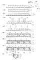
- FIG. 1A to 1I are cross-sectional process diagrams illustrating a method for manufacturing an embodiment of the wavelength conversion member of the present invention.
- FIG. 1A is a process for preparing a green sheet
- FIG. 1B is a process for firing the green sheet.
- 1C is a step of disposing the phosphor ceramic layer on the substrate
- FIG. 1D is a step of scraping a part of the phosphor ceramic layer
- FIG. 1E is a step of obtaining a phosphor ceramic element
- FIG. FIG. 1G shows a step of forming a coating layer
- FIG. 1H shows a step of cutting the coating layer and the substrate
- FIG. 1I shows a step of obtaining a wavelength conversion member.
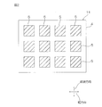
- FIG. 2 shows a plan view of the process of FIG.
- FIG. 3 is a cross-sectional view of a semiconductor light emitting device including an embodiment of the wavelength conversion member of the present invention.
- 4A to 4E are cross-sectional process diagrams illustrating a method of manufacturing another embodiment of the wavelength conversion member of the present invention (a form in which the phosphor ceramic element has a trapezoidal shape in cross section), and FIG. Fig. 4B is a step of obtaining a phosphor ceramic element, Fig. 4C is a step of forming a coating layer, Fig. 4D is a step of cutting the coating layer and the substrate, Fig. 4B is a step of scraping a part of the phosphor ceramic layer. 4E shows the process of obtaining a wavelength conversion member.
- FIG. 5A and 5B are cross-sectional process diagrams illustrating a method of manufacturing another embodiment of the wavelength conversion member of the present invention (a form in which a coating layer is coated only on the side surface of the phosphor ceramic element).
- FIG. 5A shows a step of forming a coating layer
- FIG. 5B shows a step of obtaining a wavelength conversion member.
- a method for manufacturing the wavelength conversion member 1 will be described with reference to FIGS. 1A to 1I.
- 1A to 1I is the “vertical direction” (first direction, thickness direction), the upper side of the paper is the upper side, and the lower side of the paper is the lower side.
- 1A to 1I is the “width direction” (second direction, left and right direction, direction orthogonal to the first direction), and the right side of the page is the right side, and the left side of FIG. 1A to 1I is the left side of the page. The direction is on the left.
- the paper thickness direction of FIGS. 1A to 1I is the “front-rear direction” (the direction orthogonal to the third direction, the first direction, and the second direction), and the front side of the paper thickness of FIGS. 1A to 1I is the front side.
- the back side of the paper thickness in FIGS. 1A to 1I is the rear side.
- the drawings other than FIGS. 1A to 1I also refer to the directions of FIGS. 1A to 1I.
- the method of manufacturing the wavelength conversion member 1 includes a step of preparing the green sheet 2, a step of firing the green sheet 2, a step of arranging the phosphor ceramic layer 3 on the base material 4, and scraping a part of the phosphor ceramic layer 3.
- a green sheet 2 is prepared (preparation process).
- the green sheet 2 is formed, for example, by applying and drying a slurry containing a phosphor material, a binder resin, and a solvent on the upper surface of the release sheet 8.
- the phosphor material is a raw material constituting the phosphor to be described later, for example, aluminum oxide, yttrium oxide, cerium oxide, zirconium oxide, titanium oxide, and those obtained by activating other elements. It is prepared by selecting appropriately.
- a known binder resin used for producing the green sheet 2 may be used, and examples thereof include an acrylic polymer, a butyral polymer, a vinyl polymer, and a urethane polymer.
- an acrylic polymer is used.
- the content ratio of the binder resin is, for example, 5% by volume or more, preferably 20% by volume or more, and 80% by volume or less, preferably 60% with respect to the total volume of the phosphor material and the binder resin. % By volume or less.
- the solvent examples include water and organic solvents such as acetone, methyl ethyl ketone, methanol, ethanol, toluene, methyl propionate, and methyl cellosolve.
- the content ratio of the solvent is, for example, 1 to 30% by mass in the slurry.
- the slurry can contain known additives such as a dispersant, a plasticizer, and a sintering aid, if necessary.
- the slurry is applied to the upper surface of the release sheet 8 by a known application method such as a doctor blade, a gravure coater, a fountain coater, a cast coater, a spin coater, or a roll coater, and dried to form the green sheet 2.
- a known application method such as a doctor blade, a gravure coater, a fountain coater, a cast coater, a spin coater, or a roll coater, and dried to form the green sheet 2.
- a polyester film such as a polyethylene terephthalate (PET) film, for example, a polycarbonate film, for example, a polyolefin film such as a polyethylene film or a polypropylene film, for example, a polystyrene film, for example, an acrylic film, for example, silicone
- PET polyethylene terephthalate
- the resin film include resin films and fluororesin films.
- metal foils such as copper foil and stainless steel foil, are also mentioned, for example.
- a resin film is preferable, and a polyester film is more preferable.
- the surface of the release sheet 8 is subjected to release treatment as necessary in order to improve the release property.
- the thickness of the release sheet 8 is, for example, 10 to 200 ⁇ m from the viewpoint of handling properties and cost.
- the green sheet 2 obtained in this way is a pre-sintered ceramic of the phosphor ceramic layer 3 (phosphor ceramic plate) and is formed in a flat plate shape having a substantially rectangular shape in plan view.
- the green sheet 2 can also be formed by laminating a plurality (multi-layer) of green sheets 2 by thermal lamination.
- the thickness of the green sheet 2 is, for example, 10 ⁇ m or more, preferably 30 ⁇ m or more, and for example, 500 ⁇ m or less, preferably 200 ⁇ m or less.
- the green sheet 2 is fired (firing step).
- Calcination temperature is, for example, 1300 ° C. or higher, preferably 1500 ° C. or higher, and for example, 2000 ° C. or lower, preferably 1800 ° C. or lower.
- Calcination time is, for example, 1 hour or more, preferably 2 hours or more, and for example, 24 hours or less, preferably 5 hours or less.
- Calcination may be performed under normal pressure, or may be performed under reduced pressure or under vacuum.
- preheating is performed in the air at, for example, 600 to 1300 ° C. using an electric furnace to remove the binder. Processing may be performed.
- the rate of temperature increase in the firing is, for example, 0.5 to 20 ° C./min.
- the phosphor ceramic layer 3 thus obtained is formed in a flat plate shape having a substantially rectangular shape in plan view.
- the thickness of the phosphor ceramic layer 3 is, for example, 10 ⁇ m or more, preferably 50 ⁇ m or more, and, for example, 500 ⁇ m or less, preferably 200 ⁇ m or less.
- the phosphor ceramic layer 3 is disposed on the substrate 4 (arrangement step). Specifically, the phosphor ceramic layer 3 is disposed at a substantially central portion on the upper surface of the substrate 4.
- the base material 4 is preferably an easily peelable sheet from the viewpoint of scraping of a blade (described later) and the peelability of the base material 4 with respect to the wavelength conversion member 1.
- the easily peelable sheet is formed from, for example, a heat peelable sheet that can be easily peeled off by heating or the like.
- the heat release sheet includes a support layer and an adhesive layer laminated on the upper surface of the support layer.
- the support layer is made of a heat resistant resin such as polyester.
- the pressure-sensitive adhesive layer is formed of, for example, a thermally expandable pressure-sensitive adhesive that has adhesiveness at room temperature (25 ° C.) and that reduces (or loses) adhesiveness when heated.
- thermo release sheet Commercially available products can be used as the thermal release sheet, and specifically, Riva Alpha series (registered trademark, manufactured by Nitto Denko Corporation) can be used.
- the thermal release sheet is wavelength-converted based on the decrease in the adhesive layer's adhesiveness due to heating, while the support layer reliably supports the phosphor ceramic layer 3 (and thus the wavelength conversion member 1) via the adhesive layer. It is peeled from the member 1.
- the substrate 4 is made of, for example, a polyolefin (specifically, polyethylene, polypropylene), a vinyl polymer such as ethylene / vinyl acetate copolymer (EVA), for example, a polyester such as polyethylene terephthalate or polycarbonate, for example, poly You may form from resin materials, such as fluororesins, such as tetrafluoroethylene.
- the base material can also be formed from, for example, a metal material such as iron, aluminum, and stainless steel.
- the thickness of the substrate 4 is, for example, 10 to 1000 ⁇ m.
- a part of the phosphor ceramic layer 3 is removed (removal step). Specifically, a part of the phosphor ceramic layer 3 is scraped off using a dicing blade 10 as a blade.
- the dicing blade 10 is a disk-shaped rotary blade used in a known or commercially available dicing apparatus.
- the front end (lower end) of the dicing blade 10 is formed in a substantially rectangular shape (plate shape) extending in the vertical direction when projected in a direction along the cutting direction (in FIG. 1D, the front-rear direction being the paper thickness direction). . That is, the cut surface is formed in a substantially rectangular shape.
- the width direction length X at the tip of the dicing blade 10 is, for example, 0.05 mm or more, preferably 0.1 mm or more, for example, 2.0 mm or less, preferably 1.0 mm or less.
- the ceramic laminate 9 is disposed in the dicing apparatus so that the cutting direction is the front-rear direction. Subsequently, the dicing blade 10 or the ceramic laminate 9 is arranged so that the tip (lower end) of the dicing blade 10 is in contact with the phosphor ceramic layer 3 and does not penetrate the base material 4 when the dicing blade 10 is moved. adjust. That is, the vertical position of the dicing blade 10 or the ceramic laminate 9 is adjusted so that the tip of the dicing blade 10 reaches the upper surface of the substrate 4 and does not reach the lower surface of the substrate 4. Subsequently, the dicing blade 10 is moved in the front-rear direction along the cutting direction while rotating at high speed.
- the portion of the phosphor ceramic layer 3 in contact with the dicing blade 10 (around the tip) is scraped from the base material 4 along the front-rear direction. That is, the phosphor ceramic layer 3 is scraped off into a substantially rectangular shape. In the scraped portion, the upper surface of the substrate 4 is exposed.
- the scraping in the front-rear direction is repeatedly performed at a desired interval (that is, a desired length in the width direction of the phosphor ceramic element 5) as indicated by an imaginary line in FIG. 1D.
- the phosphor ceramic layer 3 is scraped off in a lattice shape.
- an element arrangement substrate 11 including the substrate 4 and a plurality of phosphor ceramic elements 5 arranged in a lattice pattern on the upper surface of the substrate 4 is obtained.
- the phosphor ceramic layer 3 is fixed and the dicing blade 10 is moved to scrape a part of the phosphor ceramic layer 3.
- the position of the dicing blade 10 rotating at high speed is removed.
- a part of the phosphor ceramic layer 3 can also be scraped off by moving the ceramic laminate 9 in the front-rear direction or the width direction with respect to the dicing blade 10 by an XY stage or the like.
- Each of the phosphor ceramic elements 5 is formed in a substantially rectangular shape in sectional view and a substantially rectangular shape in plan view.
- the length Y in the width direction of the phosphor ceramic element 5 is, for example, 0.2 mm or more, preferably 1.0 mm or more, and, for example, 10 mm or less, preferably 5 mm or less.
- the longitudinal length of the phosphor ceramic element 5 is, for example, 0.05 mm or more, preferably 0.1 mm or more, and for example, 5 mm or less, preferably 3 mm or less.
- the interval in the width direction and the interval in the front-rear direction of the plurality of phosphor ceramic elements 5 are the same as the length X in the width direction of the tip of the dicing blade 10.
- a coating layer 7 containing an inorganic substance is formed on the base material 4 so as to cover the surface of the phosphor ceramic element 5 (formation step).
- a curable composition containing an inorganic substance is applied onto the base material 4 by a known method so as to cover the upper surface and side surfaces of the phosphor ceramic element 5, and cured.
- the curable layer 6 is formed (curable layer forming step).
- the curable composition is not limited as long as it contains an inorganic substance and has curability, and includes, for example, a ceramic ink, a curable resin composition containing a curable resin and inorganic particles, an alkali metal silicate, and An aqueous silicate solution containing inorganic particles may be mentioned.
- the ceramic ink contains, for example, an inorganic ceramic, a binder such as organopolysiloxane, and a solvent, and is cured (solidified) at a low temperature (for example, 120 to 180 ° C.).
- the inorganic substance in the ceramic ink include white pigments such as silicon dioxide, titanium dioxide, and potassium titanate.
- the solvent include ethers such as butyl diglycol ether and diethylene glycol dibutyl ether. From the viewpoint of dispersibility, the white pigment is preferably surface-treated.
- Ceramic ink Commercially available products can be used as the ceramic ink, and specific examples include ceramic inks (RG type, AN type, UV type, SD type) manufactured by Ein Co., Ltd.
- curable resin contained in the curable resin composition examples include a curable silicone resin, an epoxy resin, and an acrylic resin.
- a curable silicone resin is used.
- curable silicone resin examples include a condensation reaction curable silicone resin and an addition reaction curable silicone resin.
- an addition reaction curable silicone resin is used.
- the addition reaction curable silicone resin is composed of, for example, a silicone resin composition containing an ethylenically unsaturated hydrocarbon group-containing polysiloxane as a main agent and an organohydrogensiloxane as a crosslinking agent.
- the addition reaction curable silicone resin is usually provided as two liquids, liquid A containing a main agent (ethylenically unsaturated hydrocarbon group-containing polysiloxane) and liquid B containing a crosslinking agent (organohydrogensiloxane).
- the addition reaction curable silicone resin is cured to form a silicone elastomer (cured body).
- the inorganic substance constituting the inorganic particles include inorganic oxides such as silicon dioxide, titanium dioxide, aluminum oxide, zirconium oxide, and titanic acid complex oxides (eg, barium titanate and potassium titanate), such as silver and aluminum. And the like. From the viewpoint of light reflectivity and heat dissipation, preferably, titanium dioxide, aluminum oxide, zirconium oxide, barium titanate, and silver are mentioned. From the viewpoint of long-term heat resistance, more preferably, titanium dioxide, aluminum oxide, and zirconium oxide. And barium titanate are preferable, and titanium dioxide and aluminum oxide are more preferable.
- inorganic oxides such as silicon dioxide, titanium dioxide, aluminum oxide, zirconium oxide, and titanic acid complex oxides (eg, barium titanate and potassium titanate), such as silver and aluminum. And the like. From the viewpoint of light reflectivity and heat dissipation, preferably, titanium dioxide, aluminum oxide, zirconium oxide, barium titanate, and silver are mentioned. From the viewpoint of long-term heat
- the average particle diameter (average maximum length) of the inorganic particles is, for example, 0.1 to 50 ⁇ m.
- the curable resin composition preferably contains inorganic particles composed of at least one selected from the group consisting of titanium dioxide, aluminum oxide, zirconium oxide, barium titanate and silver, and a curable silicone resin. And more preferably inorganic particles composed of at least one selected from the group consisting of titanium dioxide, aluminum oxide, zirconium oxide and barium titanate, and a curable silicone resin.
- the curable resin composition containing is mentioned, More preferably, the inorganic particle comprised from at least 1 sort (s) of titanium dioxide and aluminum oxide, and the curable resin composition containing a curable silicone resin are mentioned.
- Examples of the alkali metal silicate contained in the silicate aqueous solution include sodium silicate (water glass).
- the content (solid content) of the inorganic substance in the curable composition is, for example, 30% by mass or more, preferably 40% by mass or more, more preferably 60% by mass or more, for example, 90% by mass or less, preferably 80% by mass or less.
- the content ratio (solid content) of the binder or curable resin in the curable composition is, for example, 10% by mass or more, preferably 20% by mass or more, for example, 70% by mass or less, preferably 60% by mass or less. More preferably, it is 40% by mass or less.
- the curable composition is preferably a ceramic ink; a curable resin composition containing at least one inorganic particle of inorganic oxide particles and metal particles and a curable resin, more preferably a ceramic ink; A curable resin composition containing inorganic oxide particles and a curable resin is exemplified, and ceramic ink is more preferable. Thereby, the heat dissipation of the coating layer 7 and reflectivity can be improved.
- Examples of the application method of the curable composition include known application methods such as printing and dispenser.
- the base material 4, the plurality of phosphor ceramic elements 5 arranged in alignment on the base material 4, and the top surface and side surfaces of the plurality of phosphor ceramic elements 5 are covered.
- a curable layer-element laminate 12 including the curable layer 6 formed thereon is obtained.
- a coating layer 7 is formed (coating layer forming step). Specifically, the coating layer 7 is formed by curing (solidifying) the curable layer 6 by heating.
- the heating temperature is, for example, 100 ° C. or more, preferably 120 ° C. or more, and for example, 200 ° C. or less, preferably 180 ° C. or less.
- the heating time is, for example, 0.5 hours or more, preferably 1 hour or more, and for example, 12 hours or less, preferably 6 hours or less.
- the drying step can be performed, for example, under conditions of 50 to 100 ° C. and 1 to 10 hours before heat curing.
- the curable layer 6 is heat-cured and the coating layer 7 is formed.
- the coating layer 7 and the base material 4 are cut in the thickness direction so as to include one phosphor ceramic element 5 (cutting step). That is, the phosphor ceramic elements 5 are cut into a plurality of phosphor ceramic elements 5 and separated (individualized).
- the coating layer 7 and the substrate 4 are cut by dicing using the narrow blade 19 along the thickness direction.
- the narrow blade 19 is a blade having a narrower width than the dicing blade 10, and is a disk-shaped rotary blade used in a known or commercially available dicing apparatus.
- the narrow blade 19 is formed in a substantially rectangular shape (plate shape) extending in the vertical direction when projected in a direction along the cutting direction (in FIG. 1H, the front-back direction which is the paper thickness direction).
- the width direction length Z of the narrow blade 19 is narrower than the width direction length X of the dicing blade 10, for example, 80% or less of X, preferably 60% or less, and for example, 10% or more, Preferably, it is 30% or more. Specifically, it is 0.01 mm or more, for example, Preferably, it is 0.05 mm or more, for example, is 1.5 mm or less, Preferably, it is 0.8 mm or less.
- the coating layer-element stack 13 is placed in a dicing apparatus. Subsequently, the arrangement of the narrow blade 19 or the covering layer-element stack 13 is adjusted so that the covering layer 7 and the substrate 4 are cut in the thickness direction. That is, the vertical position of the narrow blade 19 or the coating layer-element stack 13 is adjusted so that the tip of the narrow blade 19 penetrates the coating layer 7 and reaches the lower surface of the substrate 4. Then, in the same manner as in the above removal step, while the narrow blade 19 is rotated at a high speed, it moves between the phosphor ceramic elements 5 adjacent to each other in the front-rear direction and the width direction (that is, in a lattice shape), and the coating layer 7 and the substrate 4 are cut.
- the base material laminated wavelength conversion member 14 including the base material 4, the individual phosphor ceramic elements 5, and the coating layer 7 is obtained.
- the base material 4 is peeled to obtain the wavelength conversion member 1 including the individual phosphor ceramic elements 5 and the coating layer 7.
- the phosphor ceramic element 5 is provided at substantially the center of the upper surface of the base material 4 in plan view, and is formed of phosphor ceramic (fired body).
- the phosphor contained in the phosphor ceramic has a wavelength conversion function, for example, a yellow phosphor capable of converting blue light into yellow light, and a red fluorescence capable of converting blue light into red light. Examples include the body.
- yellow phosphor examples include silicate phosphors such as (Ba, Sr, Ca) 2 SiO 4 ; Eu, (Sr, Ba) 2 SiO 4 : Eu (barium orthosilicate (BOS)), for example, Y 3 Al Garnet-type phosphors having a garnet-type crystal structure such as 5 O 12 : Ce (YAG (yttrium, aluminum, garnet): Ce), Tb 3 Al 3 O 12 : Ce (TAG (terbium, aluminum, garnet): Ce) Examples thereof include oxynitride phosphors such as Ca- ⁇ -SiAlON. Examples of the red phosphor include nitride phosphors such as CaAlSiN 3 : Eu and CaSiN 2 : Eu.
- silicate phosphors such as (Ba, Sr, Ca) 2 SiO 4 ; Eu, (Sr, Ba) 2 SiO 4 : Eu (barium orthosilicate (BOS)
- the coating layer 7 is provided on the upper surface of the base material 4 so as to cover the surface of the phosphor ceramic element 5. Specifically, the surface of the base material 4 is coated so as to cover the surface (upper surface and side surface) of the phosphor ceramic element 5 and the upper surface of the base material 4 (excluding the surface on which the phosphor ceramic element 5 is disposed). It is provided on the upper surface.
- the thickness of the coating layer 7 (distance T from the upper surface of the phosphor ceramic element 5 to the upper surface of the coating layer 7 in FIG. 1I) is, for example, 10 ⁇ m or more, preferably 50 ⁇ m or more, and, for example, 500 ⁇ m or less, preferably Is 200 ⁇ m or less.
- the width of the side surface of the coating layer 7 (distance W from the side surface of the phosphor ceramic element 5 to the outer surface of the coating layer 7 in FIG. 1I) is, for example, 10 ⁇ m or more, preferably 50 ⁇ m or more, and, for example, 500 ⁇ m. Hereinafter, it is preferably 200 ⁇ m or less.
- the coating layer 7 is formed from a composition containing an inorganic substance as described above.
- the covering layer 7 preferably has a role as a heat dissipation layer and a reflection layer.
- the thermal conductivity of the coating layer 7 exceeds 0.20 W / m ⁇ K, preferably 1.0 W / m ⁇ K or more, more preferably 3.0 W / m ⁇ K or more. 30.0 W / m ⁇ K or less.
- the thermal conductivity is determined by a xenon flash analyzer (LFA447 manufactured by NETZSCH).
- the reflectance of the coating layer 7 is, for example, 80% or more, preferably 90% or more, and, for example, 100% or less.
- the reflectance is obtained by measuring the reflection of light having a wavelength of 450 nm using an ultraviolet-visible spectrophotometer (“V670”, manufactured by JASCO Corporation).
- the wavelength conversion member 1 is, for example, a semiconductor light-emitting device (for example, a light-emitting diode device or a semiconductor laser device) for long-distance illumination including a high-output light source such as an in-vehicle lamp, a high ceiling hanging lamp, a road lamp, or a performance lamp. Used for.
- a semiconductor light-emitting device for example, a light-emitting diode device or a semiconductor laser device
- a high-output light source such as an in-vehicle lamp, a high ceiling hanging lamp, a road lamp, or a performance lamp. Used for.
- the semiconductor light emitting device 15 includes a light source 16 and a wavelength conversion heat radiating member 17.
- Examples of the light source 16 include a light emitting diode (LED) and a semiconductor laser (LD).
- LED light emitting diode
- LD semiconductor laser
- the wavelength conversion heat radiating member 17 is disposed to face the light source 16 with a space therebetween, and includes the wavelength conversion member 1 and the heat radiating member 18.
- the heat radiation member 18 is provided on the surface (lower surface) of the coating layer 7 of the wavelength conversion member 1.
- the heat dissipating member 18 is formed in a substantially rectangular flat plate shape in plan view, and a plurality of convex portions for improving heat dissipating properties are provided on the lower surface toward the lower side.
- the heat radiating member 18 is, for example, a heat sink, and is formed of, for example, a heat conductive metal such as aluminum or copper, or a ceramic material such as AlN.
- the heat radiating member 18 can radiate the heat generated in the wavelength conversion member 1 to the outside.
- the wavelength conversion heat radiating member 17 adheres the heat radiating member 18 to the surface of the coating layer 7 of the wavelength conversion member 1 through a known heat conductive adhesive layer (not shown), and then heats the substrate. 4 is peeled off from the coating layer 7 and the phosphor ceramic element 5.
- the fluorescent substance layer is formed from the fluorescent substance ceramic element 5, it is excellent in heat resistance and heat dissipation.
- the coating layer 7 that covers the phosphor ceramic element 5 contains an inorganic substance, heat generated in the phosphor ceramic element 5 can be efficiently conducted to the outside through the coating layer 7, and heat dissipation is excellent. Moreover, the light diffused and emitted by the phosphor ceramic element 5 can be efficiently reflected.
- the wavelength conversion member 1 provided with the separated phosphor ceramic element 5 and excellent in heat resistance, heat dissipation, and reflectivity is manufactured simply and industrially. Can do.
- a part of the phosphor ceramic layer 3 is scraped off using a dicing blade 10 having a substantially rectangular cross-sectional view.
- a dicing blade 10 having a substantially rectangular cross-sectional view.
- a part of the phosphor ceramic layer 3 can be scraped off using the dicing blade 10a.
- the tip of the dicing blade 10a penetrates the phosphor ceramic layer 3 so that the dicing blade 10a can reach the inside of the substrate 4.
- the ceramic laminated body 9 is arrange
- the vertical position of the dicing blade 10 or the ceramic laminate 9 is adjusted so that the tip of the dicing blade 10a reaches the upper surface of the substrate 4 and does not reach the lower surface of the substrate 4.
- the triangular dicing blade 10 a is moved in the front-rear direction, and the phosphor ceramic layer 3 in contact with the triangular dicing blade 10 a is scraped off from the upper surface of the substrate 4.
- the triangular dicing blade 10 a is moved in the width direction, and a part of the phosphor ceramic layer 3 is scraped off from the base material 4. That is, the phosphor ceramic layer 3 is scraped off in a lattice shape.
- an element arrangement base 11 including the base 4 and a plurality of phosphor ceramic elements 5 arranged in a grid on the base 4 is obtained.
- the phosphor ceramic element 5 obtained in FIG. 4B is formed in a substantially trapezoidal shape in sectional view with a width becoming narrower toward the upper side. Further, a triangular recess 20 corresponding to the tip shape of the triangular dicing blade 10a is formed on the upper surface of the substrate 4.
- a coating layer 7 is formed so as to cover the upper surface and side surfaces of the phosphor ceramic element 5, 13 is obtained.
- the coating layer 7 and the base material 4 are arranged in the thickness direction so as to include one phosphor ceramic element 5 using a narrow blade 19. Disconnect.
- the narrow blade 19 whose width direction length is shorter than the width direction length of the recessed part 20 is used.
- the wavelength conversion member 1 including the singulated sectional substantially trapezoidal phosphor ceramic element 5 and the coating layer 7 is obtained.
- FIGS. 1A to 1I also have the same operational effects as the embodiments of FIGS. 1A to 1I.
- the coating layer 7 is formed so as to cover the upper surface and the side surface of the phosphor ceramic element 5, but for example, as shown in FIG. 5A, only the side surface of the phosphor ceramic element 5 is formed.
- the covering layer 7 can also be formed so as to cover it.
- the coating layer 7 is formed so as to cover the entire side surface of the phosphor ceramic element 5 without covering the upper surface of the phosphor ceramic element 5.
- the covering layer 7 is formed so that the upper surface of the covering layer 7 is flush with the upper surface of the phosphor ceramic element 5.
- the coating layer 7 and the base material 4 were cut in the thickness direction so as to include one phosphor ceramic element 5, and separated into pieces as shown in FIG. 5B.
- a wavelength conversion member 1 including the phosphor ceramic element 5 is obtained.
- the wavelength conversion member 1 includes a phosphor ceramic element 5 whose upper surface is exposed and a coating layer 7 that covers the side surface of the phosphor ceramic element 5.
- FIGS. 5A to 5B also has the same effect as the embodiment of FIGS. 1A to 1I.
- a part of the phosphor ceramic layer 3 is scraped off by using one dicing blade 10, but for example, although not shown, the phosphor ceramic layer 3 is used by using a plurality of dicing blades 10. You can also scrape a part of That is, the plurality of dicing blades 10 or the ceramic laminate 9 can be simultaneously moved while the plurality of dicing blades 10 are arranged at intervals in the width direction or the front-rear direction and the plurality of dicing blades are rotated at a high speed.
- the coating layer 7 and the base material 4 are cut so as to include one phosphor ceramic element 5.
- one phosphor ceramic element 5 For example, although not illustrated, two or more phosphor ceramic elements 5 are included.
- the coating layer 7 and the substrate 4 can be cut.
- a phosphor comprising 11.34 g of yttrium oxide particles (purity 99.9%, manufactured by Japan Yttrium Co.), 8.577 g of aluminum oxide particles (purity 99.9%, manufactured by Sumitomo Chemical Co., Ltd.), and 0.087 g of cerium oxide particles.
- a powder of material was prepared.
- the prepared slurry was tape-cast by a doctor blade method and dried on a PET film 8 as a release sheet to form a green sheet 2 having a thickness of 75 ⁇ m (see FIG. 1A). Then, the green sheet 2 was peeled from the PET film 8, and the green sheet 2 was cut out to a size of 20 mm ⁇ 20 mm. Two cut green sheets 2 were produced, and the two green sheets 2 were heat-laminated using a hot press to produce a green sheet laminate 2.
- the produced green sheet laminate 2 is heated to 1200 ° C. in the air at a heating rate of 1 ° C./min in an electric muffle furnace, and a binder removal process for decomposing and removing organic components such as a binder resin is performed. did. Thereafter, the green sheet laminate 2 is transferred to a high-temperature vacuum furnace and heated to 1750 ° C. at a rate of temperature increase of 5 ° C./min under a reduced pressure of about 10 ⁇ 3 Torr (about 0.13 Pa), and at that temperature for 3 hours. By firing, a phosphor ceramic layer 3 (phosphor ceramic plate) made of Y 3 Al 5 O 12 : Ce having a thickness of 120 ⁇ m was produced (see FIG. 1B).
- the phosphor ceramic layer 3 is subjected to heat release sheet 4 (base material, product name “Riva Alpha 31950”, manufactured by Nitto Denko Corporation) installed in a dicing frame of a dicing apparatus (product name “dicing saw”, manufactured by DISCO). ) was adhered to the adhesive layer surface (upper surface) to obtain a ceramic laminate 9 (see FIG. 1C).
- the vertical position of the dicing blade 10 (tip width X: 0.4 mm) whose tip is substantially rectangular in cross-section was adjusted so that the tip of the dicing blade 10 coincided with the upper surface of the thermal release sheet 4.
- the dicing blade 10 is moved relative to the ceramic laminate 9 so that each of the interval in the width direction (Y) and the interval in the front-rear direction becomes 3.0 mm. A part of the phosphor ceramic layer 3 was scraped off in a lattice pattern (see FIG. 1D).
- a ceramic ink (trade name “RG12-22”, white, manufactured by Ein Co., Ltd.) is prepared as a material for the curable layer 6, and is coated with a doctor blade so as to cover the upper surface and side surfaces of the phosphor ceramic element 5.
- the curable layer 6 was formed by coating. Thereby, a curable layer-element laminate 12 was obtained (see FIG. 1F).
- the curable layer-element laminate 12 was dried at 90 ° C. for 5 hours and then heat-cured at 150 ° C. for 2 hours to form a coating layer 7 (thickness 100 ⁇ m). As a result, a coating layer-element laminate 13 was obtained (see FIG. 1G).
- the coating layer-element stack 13 was placed in the dicing apparatus. Thereafter, using a narrow blade 19 (tip width Z: 0.2 mm) whose tip is substantially rectangular in cross-section, the width direction center and the front-rear direction center between the phosphor ceramic elements 5 are separated from the coating layer 7 and the thermal separation. It cut
- seat 4 (refer FIG. 1H). That is, the covering layer-element stack 13 was cut to a size of 3.2 mm ⁇ 3.2 mm. Thereby, the phosphor ceramic element 5 was separated into pieces, and the base material laminated wavelength conversion member 14 was obtained.
- the heat release sheet 4 was peeled off at 200 ° C. from the obtained base material laminated wavelength conversion member 14. Thereby, one phosphor ceramic element 5 (3.0 mm ⁇ 3.0 mm, thickness 120 ⁇ m) and coating layer 7 (3.2 mm ⁇ 3.2 mm, side width W: 0.1 mm, thickness T: 100 ⁇ m) are provided.
- a wavelength conversion member 1 was produced (see FIG. 1I).
- the wavelength conversion member and the manufacturing method thereof of the present invention can be applied to various industrial products, and can be used for semiconductor light emitting devices such as white light emitting diode devices, for example.
Landscapes
- Chemical & Material Sciences (AREA)
- Engineering & Computer Science (AREA)
- Ceramic Engineering (AREA)
- Manufacturing & Machinery (AREA)
- Organic Chemistry (AREA)
- Materials Engineering (AREA)
- Structural Engineering (AREA)
- Inorganic Chemistry (AREA)
- General Engineering & Computer Science (AREA)
- Physics & Mathematics (AREA)
- Microelectronics & Electronic Packaging (AREA)
- Optics & Photonics (AREA)
- Led Device Packages (AREA)
- Luminescent Compositions (AREA)
- Compositions Of Oxide Ceramics (AREA)
Abstract
Description
以降の各図において、上記した各部に対応する部材については、同一の参照符号を付し、その詳細な説明を省略する。
3 蛍光体セラミックス層
4 基材
5 蛍光体セラミックス素子
7 被覆層
10 ダイシングブレード
Claims (5)
- 蛍光体セラミックス層を基材の上に配置する配置工程、
前記基材の厚み方向と直交する方向に間隔を隔てて複数の蛍光体セラミックス素子が配置されるように、前記蛍光体セラミックス層の一部を除去する除去工程、
前記蛍光体セラミックス素子の表面を被覆するように、前記基材の上に、無機物を含有する被覆層を形成する形成工程、ならびに、
少なくとも1つの前記蛍光体セラミックス素子を含むように、前記被覆層および前記基材を厚み方向に切断する切断工程
を備えることを特徴とする、波長変換部材の製造方法。 - 前記形成工程が、セラミックスインク、または、無機酸化物粒子および金属粒子の少なくとも1種の無機粒子ならびに硬化性樹脂を含有する硬化性樹脂組成物を、前記基材の上に塗布し、硬化させる工程を備えることを特徴とする、請求項1に記載の波長変換部材の製造方法。
- 前記除去工程が、前記蛍光体セラミックス層の一部を、ブレードを用いて掻き取る工程を備えることを特徴とする、請求項1に記載の波長変換部材の製造方法。
- 前記基材が、易剥離性シートであることを特徴とする、請求項1に記載の波長変換部材の製造方法。
- 請求項1に記載の製造方法により得られることを特徴とする、波長変換部材。
Priority Applications (4)
| Application Number | Priority Date | Filing Date | Title |
|---|---|---|---|
| KR1020167029216A KR20160148535A (ko) | 2014-04-23 | 2015-04-02 | 파장 변환 부재 및 그 제조 방법 |
| US15/303,773 US20170030556A1 (en) | 2014-04-23 | 2015-04-02 | Wavelength conversion member and production method thereof |
| CN201580021239.XA CN106233475A (zh) | 2014-04-23 | 2015-04-02 | 波长转换构件及其制造方法 |
| EP15782566.2A EP3136452A4 (en) | 2014-04-23 | 2015-04-02 | Wavelength conversion member and method for manufacturing same |
Applications Claiming Priority (4)
| Application Number | Priority Date | Filing Date | Title |
|---|---|---|---|
| JP2014089576 | 2014-04-23 | ||
| JP2014-089576 | 2014-04-23 | ||
| JP2015-039034 | 2015-02-27 | ||
| JP2015039034A JP2015216354A (ja) | 2014-04-23 | 2015-02-27 | 波長変換部材およびその製造方法 |
Publications (1)
| Publication Number | Publication Date |
|---|---|
| WO2015163109A1 true WO2015163109A1 (ja) | 2015-10-29 |
Family
ID=54332277
Family Applications (1)
| Application Number | Title | Priority Date | Filing Date |
|---|---|---|---|
| PCT/JP2015/060517 Ceased WO2015163109A1 (ja) | 2014-04-23 | 2015-04-02 | 波長変換部材およびその製造方法 |
Country Status (7)
| Country | Link |
|---|---|
| US (1) | US20170030556A1 (ja) |
| EP (1) | EP3136452A4 (ja) |
| JP (1) | JP2015216354A (ja) |
| KR (1) | KR20160148535A (ja) |
| CN (1) | CN106233475A (ja) |
| TW (1) | TW201541671A (ja) |
| WO (1) | WO2015163109A1 (ja) |
Cited By (4)
| Publication number | Priority date | Publication date | Assignee | Title |
|---|---|---|---|---|
| CN105826457A (zh) * | 2016-05-18 | 2016-08-03 | 中国人民大学 | 用于照明或显示的激光白光发光装置 |
| JP6632108B1 (ja) * | 2018-09-28 | 2020-01-15 | 日本碍子株式会社 | 蛍光体素子、その製造方法および照明装置 |
| WO2020066077A1 (ja) * | 2018-09-28 | 2020-04-02 | 日本碍子株式会社 | 蛍光体素子、その製造方法および照明装置 |
| US11262046B2 (en) | 2019-03-27 | 2022-03-01 | Ngk Insulators, Ltd. | Phosphor element, method for producing same, and lighting device |
Families Citing this family (4)
| Publication number | Priority date | Publication date | Assignee | Title |
|---|---|---|---|---|
| JPWO2017056470A1 (ja) * | 2015-09-29 | 2018-07-19 | パナソニックIpマネジメント株式会社 | 波長変換素子及び発光装置 |
| CN109838763B (zh) * | 2017-09-13 | 2021-04-30 | 深圳光峰科技股份有限公司 | 一种波长转换装置及其制备方法 |
| KR102488528B1 (ko) | 2017-09-20 | 2023-01-17 | 마테리온 프레시젼 옵틱스 (상하이) 리미티드 | 무기질 바인더를 갖는 인광체 휠 |
| CN113568262A (zh) * | 2020-04-29 | 2021-10-29 | 中强光电股份有限公司 | 波长转换装置及其制造方法 |
Citations (2)
| Publication number | Priority date | Publication date | Assignee | Title |
|---|---|---|---|---|
| JP2013030720A (ja) * | 2011-07-29 | 2013-02-07 | Sharp Corp | 発光素子、発光装置および発光素子の製造方法 |
| WO2014014007A1 (ja) * | 2012-07-17 | 2014-01-23 | 日東電工株式会社 | 封止層被覆半導体素子および半導体装置の製造方法 |
Family Cites Families (10)
| Publication number | Priority date | Publication date | Assignee | Title |
|---|---|---|---|---|
| US7682850B2 (en) * | 2006-03-17 | 2010-03-23 | Philips Lumileds Lighting Company, Llc | White LED for backlight with phosphor plates |
| US8481977B2 (en) * | 2006-03-24 | 2013-07-09 | Goldeneye, Inc. | LED light source with thermally conductive luminescent matrix |
| WO2009098654A1 (en) * | 2008-02-08 | 2009-08-13 | Koninklijke Philips Electronics N.V. | Optical element and manufacturing method therefor |
| JP5395097B2 (ja) * | 2009-01-13 | 2014-01-22 | 株式会社小糸製作所 | 発光モジュールおよび灯具ユニット |
| JP5566785B2 (ja) * | 2010-06-22 | 2014-08-06 | 日東電工株式会社 | 複合シート |
| JP5766411B2 (ja) * | 2010-06-29 | 2015-08-19 | 日東電工株式会社 | 蛍光体層および発光装置 |
| US20120081000A1 (en) * | 2010-10-05 | 2012-04-05 | Power Data Communications Co., Ltd. | Led encapsulation process and shield structure made thereby |
| JP5336564B2 (ja) * | 2010-10-29 | 2013-11-06 | シャープ株式会社 | 発光装置、照明装置、車両用前照灯および車両 |
| JP2013102078A (ja) * | 2011-11-09 | 2013-05-23 | Stanley Electric Co Ltd | 光源装置および照明装置 |
| JP6033557B2 (ja) | 2012-03-06 | 2016-11-30 | 日東電工株式会社 | 封止シート、および、それを用いた発光ダイオード装置の製造方法 |
-
2015
- 2015-02-27 JP JP2015039034A patent/JP2015216354A/ja active Pending
- 2015-04-02 CN CN201580021239.XA patent/CN106233475A/zh active Pending
- 2015-04-02 KR KR1020167029216A patent/KR20160148535A/ko not_active Withdrawn
- 2015-04-02 EP EP15782566.2A patent/EP3136452A4/en not_active Withdrawn
- 2015-04-02 WO PCT/JP2015/060517 patent/WO2015163109A1/ja not_active Ceased
- 2015-04-02 US US15/303,773 patent/US20170030556A1/en not_active Abandoned
- 2015-04-22 TW TW104112920A patent/TW201541671A/zh unknown
Patent Citations (2)
| Publication number | Priority date | Publication date | Assignee | Title |
|---|---|---|---|---|
| JP2013030720A (ja) * | 2011-07-29 | 2013-02-07 | Sharp Corp | 発光素子、発光装置および発光素子の製造方法 |
| WO2014014007A1 (ja) * | 2012-07-17 | 2014-01-23 | 日東電工株式会社 | 封止層被覆半導体素子および半導体装置の製造方法 |
Non-Patent Citations (1)
| Title |
|---|
| See also references of EP3136452A4 * |
Cited By (6)
| Publication number | Priority date | Publication date | Assignee | Title |
|---|---|---|---|---|
| CN105826457A (zh) * | 2016-05-18 | 2016-08-03 | 中国人民大学 | 用于照明或显示的激光白光发光装置 |
| JP6632108B1 (ja) * | 2018-09-28 | 2020-01-15 | 日本碍子株式会社 | 蛍光体素子、その製造方法および照明装置 |
| WO2020066077A1 (ja) * | 2018-09-28 | 2020-04-02 | 日本碍子株式会社 | 蛍光体素子、その製造方法および照明装置 |
| WO2020065927A1 (ja) * | 2018-09-28 | 2020-04-02 | 日本碍子株式会社 | 蛍光体素子、その製造方法および照明装置 |
| US11635189B2 (en) | 2018-09-28 | 2023-04-25 | Ngk Insulators, Ltd. | Phosphor element and lighting device |
| US11262046B2 (en) | 2019-03-27 | 2022-03-01 | Ngk Insulators, Ltd. | Phosphor element, method for producing same, and lighting device |
Also Published As
| Publication number | Publication date |
|---|---|
| US20170030556A1 (en) | 2017-02-02 |
| CN106233475A (zh) | 2016-12-14 |
| JP2015216354A (ja) | 2015-12-03 |
| TW201541671A (zh) | 2015-11-01 |
| KR20160148535A (ko) | 2016-12-26 |
| EP3136452A4 (en) | 2017-09-27 |
| EP3136452A1 (en) | 2017-03-01 |
Similar Documents
| Publication | Publication Date | Title |
|---|---|---|
| WO2015163109A1 (ja) | 波長変換部材およびその製造方法 | |
| JP5989268B2 (ja) | 蛍光体セラミックス、封止光半導体素子、回路基板、光半導体装置および発光装置 | |
| US10557614B2 (en) | Projector light source including wavelength conversion member having porous ceramic substrate | |
| CN102738363B (zh) | 反射树脂片、发光二极管装置及其制造方法 | |
| WO2015163108A1 (ja) | 波長変換接合部材、波長変換放熱部材および発光装置 | |
| JP5745319B2 (ja) | 蛍光反射シート、および、発光ダイオード装置の製造方法 | |
| CN108351444B (zh) | 荧光体片、使用其的发光体、光源单元、显示器及发光体的制造方法 | |
| CN109643747B (zh) | 具有聚硅氧烷材料的波长转换器、制造方法和包含其的固态照明装置 | |
| WO2015195820A1 (en) | Method of making a ceramic wavelength converter assembly | |
| WO2015163110A1 (ja) | 波長変換部材およびその製造方法 | |
| JP2017143236A (ja) | セラミックスプレート、その製造方法および光半導体装置 | |
| WO2015140854A1 (ja) | 波長変換素子の製造方法 | |
| JP6582907B2 (ja) | 波長変換素子の製造方法並びに波長変換素子及び発光装置 | |
| WO2017221608A1 (ja) | 蛍光体層シート、および、蛍光体層付光半導体素子の製造方法 | |
| WO2017138180A1 (ja) | セラミックスプレート、その製造方法および光半導体装置 | |
| WO2016132888A1 (ja) | 蛍光体セラミックスの製造方法 | |
| WO2016132890A1 (ja) | 蛍光体セラミックス、封止光半導体素子、回路基板、光半導体装置および発光装置 | |
| JP2015073140A (ja) | 発光ダイオード装置 | |
| CN105304796A (zh) | 制备光波长转换片的方法以及光波长转换片和光源 |
Legal Events
| Date | Code | Title | Description |
|---|---|---|---|
| 121 | Ep: the epo has been informed by wipo that ep was designated in this application |
Ref document number: 15782566 Country of ref document: EP Kind code of ref document: A1 |
|
| WWE | Wipo information: entry into national phase |
Ref document number: 15303773 Country of ref document: US |
|
| ENP | Entry into the national phase |
Ref document number: 20167029216 Country of ref document: KR Kind code of ref document: A |
|
| REEP | Request for entry into the european phase |
Ref document number: 2015782566 Country of ref document: EP |
|
| WWE | Wipo information: entry into national phase |
Ref document number: 2015782566 Country of ref document: EP |
|
| NENP | Non-entry into the national phase |
Ref country code: DE |