WO2015163452A1 - Substrat pour modules de puissance, substrat ayant un dissipateur thermique pour modules de puissance, et module de puissance ayant un dissipateur thermique - Google Patents
Substrat pour modules de puissance, substrat ayant un dissipateur thermique pour modules de puissance, et module de puissance ayant un dissipateur thermique Download PDFInfo
- Publication number
- WO2015163452A1 WO2015163452A1 PCT/JP2015/062544 JP2015062544W WO2015163452A1 WO 2015163452 A1 WO2015163452 A1 WO 2015163452A1 JP 2015062544 W JP2015062544 W JP 2015062544W WO 2015163452 A1 WO2015163452 A1 WO 2015163452A1
- Authority
- WO
- WIPO (PCT)
- Prior art keywords
- layer
- copper layer
- power module
- heat sink
- copper
- Prior art date
- Legal status (The legal status is an assumption and is not a legal conclusion. Google has not performed a legal analysis and makes no representation as to the accuracy of the status listed.)
- Ceased
Links
Images


Classifications
-
- H—ELECTRICITY
- H10—SEMICONDUCTOR DEVICES; ELECTRIC SOLID-STATE DEVICES NOT OTHERWISE PROVIDED FOR
- H10W—GENERIC PACKAGES, INTERCONNECTIONS, CONNECTORS OR OTHER CONSTRUCTIONAL DETAILS OF DEVICES COVERED BY CLASS H10
- H10W40/00—Arrangements for thermal protection or thermal control
- H10W40/20—Arrangements for cooling
- H10W40/25—Arrangements for cooling characterised by their materials
- H10W40/255—Arrangements for cooling characterised by their materials having a laminate or multilayered structure, e.g. direct bond copper [DBC] ceramic substrates
-
- B—PERFORMING OPERATIONS; TRANSPORTING
- B23—MACHINE TOOLS; METAL-WORKING NOT OTHERWISE PROVIDED FOR
- B23K—SOLDERING OR UNSOLDERING; WELDING; CLADDING OR PLATING BY SOLDERING OR WELDING; CUTTING BY APPLYING HEAT LOCALLY, e.g. FLAME CUTTING; WORKING BY LASER BEAM
- B23K20/00—Non-electric welding by applying impact or other pressure, with or without the application of heat, e.g. cladding or plating
- B23K20/02—Non-electric welding by applying impact or other pressure, with or without the application of heat, e.g. cladding or plating by means of a press ; Diffusion bonding
-
- C—CHEMISTRY; METALLURGY
- C04—CEMENTS; CONCRETE; ARTIFICIAL STONE; CERAMICS; REFRACTORIES
- C04B—LIME, MAGNESIA; SLAG; CEMENTS; COMPOSITIONS THEREOF, e.g. MORTARS, CONCRETE OR LIKE BUILDING MATERIALS; ARTIFICIAL STONE; CERAMICS; REFRACTORIES; TREATMENT OF NATURAL STONE
- C04B37/00—Joining burned ceramic articles with other burned ceramic articles or other articles by heating
- C04B37/02—Joining burned ceramic articles with other burned ceramic articles or other articles by heating with metallic articles
- C04B37/023—Joining burned ceramic articles with other burned ceramic articles or other articles by heating with metallic articles characterised by the interlayer used
- C04B37/026—Joining burned ceramic articles with other burned ceramic articles or other articles by heating with metallic articles characterised by the interlayer used consisting of metals or metal salts
-
- H—ELECTRICITY
- H10—SEMICONDUCTOR DEVICES; ELECTRIC SOLID-STATE DEVICES NOT OTHERWISE PROVIDED FOR
- H10F—INORGANIC SEMICONDUCTOR DEVICES SENSITIVE TO INFRARED RADIATION, LIGHT, ELECTROMAGNETIC RADIATION OF SHORTER WAVELENGTH OR CORPUSCULAR RADIATION
- H10F10/00—Individual photovoltaic cells, e.g. solar cells
-
- H—ELECTRICITY
- H10—SEMICONDUCTOR DEVICES; ELECTRIC SOLID-STATE DEVICES NOT OTHERWISE PROVIDED FOR
- H10W—GENERIC PACKAGES, INTERCONNECTIONS, CONNECTORS OR OTHER CONSTRUCTIONAL DETAILS OF DEVICES COVERED BY CLASS H10
- H10W40/00—Arrangements for thermal protection or thermal control
- H10W40/01—Manufacture or treatment
- H10W40/03—Manufacture or treatment of arrangements for cooling
- H10W40/037—Assembling together parts thereof
-
- H—ELECTRICITY
- H10—SEMICONDUCTOR DEVICES; ELECTRIC SOLID-STATE DEVICES NOT OTHERWISE PROVIDED FOR
- H10W—GENERIC PACKAGES, INTERCONNECTIONS, CONNECTORS OR OTHER CONSTRUCTIONAL DETAILS OF DEVICES COVERED BY CLASS H10
- H10W40/00—Arrangements for thermal protection or thermal control
- H10W40/20—Arrangements for cooling
- H10W40/22—Arrangements for cooling characterised by their shape, e.g. having conical or cylindrical projections
-
- H—ELECTRICITY
- H10—SEMICONDUCTOR DEVICES; ELECTRIC SOLID-STATE DEVICES NOT OTHERWISE PROVIDED FOR
- H10W—GENERIC PACKAGES, INTERCONNECTIONS, CONNECTORS OR OTHER CONSTRUCTIONAL DETAILS OF DEVICES COVERED BY CLASS H10
- H10W40/00—Arrangements for thermal protection or thermal control
- H10W40/20—Arrangements for cooling
- H10W40/22—Arrangements for cooling characterised by their shape, e.g. having conical or cylindrical projections
- H10W40/226—Arrangements for cooling characterised by their shape, e.g. having conical or cylindrical projections characterised by projecting parts, e.g. fins to increase surface area
-
- H—ELECTRICITY
- H10—SEMICONDUCTOR DEVICES; ELECTRIC SOLID-STATE DEVICES NOT OTHERWISE PROVIDED FOR
- H10W—GENERIC PACKAGES, INTERCONNECTIONS, CONNECTORS OR OTHER CONSTRUCTIONAL DETAILS OF DEVICES COVERED BY CLASS H10
- H10W40/00—Arrangements for thermal protection or thermal control
- H10W40/20—Arrangements for cooling
- H10W40/25—Arrangements for cooling characterised by their materials
- H10W40/258—Metallic materials
-
- H—ELECTRICITY
- H10—SEMICONDUCTOR DEVICES; ELECTRIC SOLID-STATE DEVICES NOT OTHERWISE PROVIDED FOR
- H10W—GENERIC PACKAGES, INTERCONNECTIONS, CONNECTORS OR OTHER CONSTRUCTIONAL DETAILS OF DEVICES COVERED BY CLASS H10
- H10W70/00—Package substrates; Interposers; Redistribution layers [RDL]
- H10W70/60—Insulating or insulated package substrates; Interposers; Redistribution layers
-
- H—ELECTRICITY
- H10—SEMICONDUCTOR DEVICES; ELECTRIC SOLID-STATE DEVICES NOT OTHERWISE PROVIDED FOR
- H10W—GENERIC PACKAGES, INTERCONNECTIONS, CONNECTORS OR OTHER CONSTRUCTIONAL DETAILS OF DEVICES COVERED BY CLASS H10
- H10W70/00—Package substrates; Interposers; Redistribution layers [RDL]
- H10W70/60—Insulating or insulated package substrates; Interposers; Redistribution layers
- H10W70/67—Insulating or insulated package substrates; Interposers; Redistribution layers characterised by their insulating layers or insulating parts
- H10W70/68—Shapes or dispositions thereof
-
- B—PERFORMING OPERATIONS; TRANSPORTING
- B23—MACHINE TOOLS; METAL-WORKING NOT OTHERWISE PROVIDED FOR
- B23K—SOLDERING OR UNSOLDERING; WELDING; CLADDING OR PLATING BY SOLDERING OR WELDING; CUTTING BY APPLYING HEAT LOCALLY, e.g. FLAME CUTTING; WORKING BY LASER BEAM
- B23K2103/00—Materials to be soldered, welded or cut
- B23K2103/08—Non-ferrous metals or alloys
- B23K2103/10—Aluminium or alloys thereof
-
- B—PERFORMING OPERATIONS; TRANSPORTING
- B23—MACHINE TOOLS; METAL-WORKING NOT OTHERWISE PROVIDED FOR
- B23K—SOLDERING OR UNSOLDERING; WELDING; CLADDING OR PLATING BY SOLDERING OR WELDING; CUTTING BY APPLYING HEAT LOCALLY, e.g. FLAME CUTTING; WORKING BY LASER BEAM
- B23K2103/00—Materials to be soldered, welded or cut
- B23K2103/08—Non-ferrous metals or alloys
- B23K2103/12—Copper or alloys thereof
-
- B—PERFORMING OPERATIONS; TRANSPORTING
- B23—MACHINE TOOLS; METAL-WORKING NOT OTHERWISE PROVIDED FOR
- B23K—SOLDERING OR UNSOLDERING; WELDING; CLADDING OR PLATING BY SOLDERING OR WELDING; CUTTING BY APPLYING HEAT LOCALLY, e.g. FLAME CUTTING; WORKING BY LASER BEAM
- B23K2103/00—Materials to be soldered, welded or cut
- B23K2103/18—Dissimilar materials
-
- C—CHEMISTRY; METALLURGY
- C04—CEMENTS; CONCRETE; ARTIFICIAL STONE; CERAMICS; REFRACTORIES
- C04B—LIME, MAGNESIA; SLAG; CEMENTS; COMPOSITIONS THEREOF, e.g. MORTARS, CONCRETE OR LIKE BUILDING MATERIALS; ARTIFICIAL STONE; CERAMICS; REFRACTORIES; TREATMENT OF NATURAL STONE
- C04B2237/00—Aspects relating to ceramic laminates or to joining of ceramic articles with other articles by heating
- C04B2237/02—Aspects relating to interlayers, e.g. used to join ceramic articles with other articles by heating
- C04B2237/12—Metallic interlayers
- C04B2237/121—Metallic interlayers based on aluminium
-
- C—CHEMISTRY; METALLURGY
- C04—CEMENTS; CONCRETE; ARTIFICIAL STONE; CERAMICS; REFRACTORIES
- C04B—LIME, MAGNESIA; SLAG; CEMENTS; COMPOSITIONS THEREOF, e.g. MORTARS, CONCRETE OR LIKE BUILDING MATERIALS; ARTIFICIAL STONE; CERAMICS; REFRACTORIES; TREATMENT OF NATURAL STONE
- C04B2237/00—Aspects relating to ceramic laminates or to joining of ceramic articles with other articles by heating
- C04B2237/02—Aspects relating to interlayers, e.g. used to join ceramic articles with other articles by heating
- C04B2237/12—Metallic interlayers
- C04B2237/126—Metallic interlayers wherein the active component for bonding is not the largest fraction of the interlayer
- C04B2237/128—The active component for bonding being silicon
-
- C—CHEMISTRY; METALLURGY
- C04—CEMENTS; CONCRETE; ARTIFICIAL STONE; CERAMICS; REFRACTORIES
- C04B—LIME, MAGNESIA; SLAG; CEMENTS; COMPOSITIONS THEREOF, e.g. MORTARS, CONCRETE OR LIKE BUILDING MATERIALS; ARTIFICIAL STONE; CERAMICS; REFRACTORIES; TREATMENT OF NATURAL STONE
- C04B2237/00—Aspects relating to ceramic laminates or to joining of ceramic articles with other articles by heating
- C04B2237/30—Composition of layers of ceramic laminates or of ceramic or metallic articles to be joined by heating, e.g. Si substrates
- C04B2237/32—Ceramic
- C04B2237/34—Oxidic
- C04B2237/343—Alumina or aluminates
-
- C—CHEMISTRY; METALLURGY
- C04—CEMENTS; CONCRETE; ARTIFICIAL STONE; CERAMICS; REFRACTORIES
- C04B—LIME, MAGNESIA; SLAG; CEMENTS; COMPOSITIONS THEREOF, e.g. MORTARS, CONCRETE OR LIKE BUILDING MATERIALS; ARTIFICIAL STONE; CERAMICS; REFRACTORIES; TREATMENT OF NATURAL STONE
- C04B2237/00—Aspects relating to ceramic laminates or to joining of ceramic articles with other articles by heating
- C04B2237/30—Composition of layers of ceramic laminates or of ceramic or metallic articles to be joined by heating, e.g. Si substrates
- C04B2237/32—Ceramic
- C04B2237/36—Non-oxidic
- C04B2237/366—Aluminium nitride
-
- C—CHEMISTRY; METALLURGY
- C04—CEMENTS; CONCRETE; ARTIFICIAL STONE; CERAMICS; REFRACTORIES
- C04B—LIME, MAGNESIA; SLAG; CEMENTS; COMPOSITIONS THEREOF, e.g. MORTARS, CONCRETE OR LIKE BUILDING MATERIALS; ARTIFICIAL STONE; CERAMICS; REFRACTORIES; TREATMENT OF NATURAL STONE
- C04B2237/00—Aspects relating to ceramic laminates or to joining of ceramic articles with other articles by heating
- C04B2237/30—Composition of layers of ceramic laminates or of ceramic or metallic articles to be joined by heating, e.g. Si substrates
- C04B2237/32—Ceramic
- C04B2237/36—Non-oxidic
- C04B2237/368—Silicon nitride
-
- C—CHEMISTRY; METALLURGY
- C04—CEMENTS; CONCRETE; ARTIFICIAL STONE; CERAMICS; REFRACTORIES
- C04B—LIME, MAGNESIA; SLAG; CEMENTS; COMPOSITIONS THEREOF, e.g. MORTARS, CONCRETE OR LIKE BUILDING MATERIALS; ARTIFICIAL STONE; CERAMICS; REFRACTORIES; TREATMENT OF NATURAL STONE
- C04B2237/00—Aspects relating to ceramic laminates or to joining of ceramic articles with other articles by heating
- C04B2237/30—Composition of layers of ceramic laminates or of ceramic or metallic articles to be joined by heating, e.g. Si substrates
- C04B2237/40—Metallic
- C04B2237/402—Aluminium
-
- C—CHEMISTRY; METALLURGY
- C04—CEMENTS; CONCRETE; ARTIFICIAL STONE; CERAMICS; REFRACTORIES
- C04B—LIME, MAGNESIA; SLAG; CEMENTS; COMPOSITIONS THEREOF, e.g. MORTARS, CONCRETE OR LIKE BUILDING MATERIALS; ARTIFICIAL STONE; CERAMICS; REFRACTORIES; TREATMENT OF NATURAL STONE
- C04B2237/00—Aspects relating to ceramic laminates or to joining of ceramic articles with other articles by heating
- C04B2237/30—Composition of layers of ceramic laminates or of ceramic or metallic articles to be joined by heating, e.g. Si substrates
- C04B2237/40—Metallic
- C04B2237/407—Copper
-
- C—CHEMISTRY; METALLURGY
- C04—CEMENTS; CONCRETE; ARTIFICIAL STONE; CERAMICS; REFRACTORIES
- C04B—LIME, MAGNESIA; SLAG; CEMENTS; COMPOSITIONS THEREOF, e.g. MORTARS, CONCRETE OR LIKE BUILDING MATERIALS; ARTIFICIAL STONE; CERAMICS; REFRACTORIES; TREATMENT OF NATURAL STONE
- C04B2237/00—Aspects relating to ceramic laminates or to joining of ceramic articles with other articles by heating
- C04B2237/50—Processing aspects relating to ceramic laminates or to the joining of ceramic articles with other articles by heating
- C04B2237/70—Forming laminates or joined articles comprising layers of a specific, unusual thickness
- C04B2237/704—Forming laminates or joined articles comprising layers of a specific, unusual thickness of one or more of the ceramic layers or articles
-
- C—CHEMISTRY; METALLURGY
- C04—CEMENTS; CONCRETE; ARTIFICIAL STONE; CERAMICS; REFRACTORIES
- C04B—LIME, MAGNESIA; SLAG; CEMENTS; COMPOSITIONS THEREOF, e.g. MORTARS, CONCRETE OR LIKE BUILDING MATERIALS; ARTIFICIAL STONE; CERAMICS; REFRACTORIES; TREATMENT OF NATURAL STONE
- C04B2237/00—Aspects relating to ceramic laminates or to joining of ceramic articles with other articles by heating
- C04B2237/50—Processing aspects relating to ceramic laminates or to the joining of ceramic articles with other articles by heating
- C04B2237/70—Forming laminates or joined articles comprising layers of a specific, unusual thickness
- C04B2237/706—Forming laminates or joined articles comprising layers of a specific, unusual thickness of one or more of the metallic layers or articles
-
- C—CHEMISTRY; METALLURGY
- C04—CEMENTS; CONCRETE; ARTIFICIAL STONE; CERAMICS; REFRACTORIES
- C04B—LIME, MAGNESIA; SLAG; CEMENTS; COMPOSITIONS THEREOF, e.g. MORTARS, CONCRETE OR LIKE BUILDING MATERIALS; ARTIFICIAL STONE; CERAMICS; REFRACTORIES; TREATMENT OF NATURAL STONE
- C04B2237/00—Aspects relating to ceramic laminates or to joining of ceramic articles with other articles by heating
- C04B2237/50—Processing aspects relating to ceramic laminates or to the joining of ceramic articles with other articles by heating
- C04B2237/86—Joining of two substrates at their largest surfaces, one surface being complete joined and covered, the other surface not, e.g. a small plate joined at it's largest surface on top of a larger plate
-
- H—ELECTRICITY
- H10—SEMICONDUCTOR DEVICES; ELECTRIC SOLID-STATE DEVICES NOT OTHERWISE PROVIDED FOR
- H10W—GENERIC PACKAGES, INTERCONNECTIONS, CONNECTORS OR OTHER CONSTRUCTIONAL DETAILS OF DEVICES COVERED BY CLASS H10
- H10W40/00—Arrangements for thermal protection or thermal control
- H10W40/40—Arrangements for thermal protection or thermal control involving heat exchange by flowing fluids
- H10W40/47—Arrangements for thermal protection or thermal control involving heat exchange by flowing fluids by flowing liquids, e.g. forced water cooling
-
- H—ELECTRICITY
- H10—SEMICONDUCTOR DEVICES; ELECTRIC SOLID-STATE DEVICES NOT OTHERWISE PROVIDED FOR
- H10W—GENERIC PACKAGES, INTERCONNECTIONS, CONNECTORS OR OTHER CONSTRUCTIONAL DETAILS OF DEVICES COVERED BY CLASS H10
- H10W72/00—Interconnections or connectors in packages
- H10W72/30—Die-attach connectors
-
- H—ELECTRICITY
- H10—SEMICONDUCTOR DEVICES; ELECTRIC SOLID-STATE DEVICES NOT OTHERWISE PROVIDED FOR
- H10W—GENERIC PACKAGES, INTERCONNECTIONS, CONNECTORS OR OTHER CONSTRUCTIONAL DETAILS OF DEVICES COVERED BY CLASS H10
- H10W72/00—Interconnections or connectors in packages
- H10W72/30—Die-attach connectors
- H10W72/351—Materials of die-attach connectors
- H10W72/352—Materials of die-attach connectors comprising metals or metalloids, e.g. solders
-
- H—ELECTRICITY
- H10—SEMICONDUCTOR DEVICES; ELECTRIC SOLID-STATE DEVICES NOT OTHERWISE PROVIDED FOR
- H10W—GENERIC PACKAGES, INTERCONNECTIONS, CONNECTORS OR OTHER CONSTRUCTIONAL DETAILS OF DEVICES COVERED BY CLASS H10
- H10W90/00—Package configurations
- H10W90/701—Package configurations characterised by the relative positions of pads or connectors relative to package parts
- H10W90/731—Package configurations characterised by the relative positions of pads or connectors relative to package parts of die-attach connectors
- H10W90/734—Package configurations characterised by the relative positions of pads or connectors relative to package parts of die-attach connectors between a chip and a stacked insulating package substrate, interposer or RDL
-
- Y—GENERAL TAGGING OF NEW TECHNOLOGICAL DEVELOPMENTS; GENERAL TAGGING OF CROSS-SECTIONAL TECHNOLOGIES SPANNING OVER SEVERAL SECTIONS OF THE IPC; TECHNICAL SUBJECTS COVERED BY FORMER USPC CROSS-REFERENCE ART COLLECTIONS [XRACs] AND DIGESTS
- Y02—TECHNOLOGIES OR APPLICATIONS FOR MITIGATION OR ADAPTATION AGAINST CLIMATE CHANGE
- Y02E—REDUCTION OF GREENHOUSE GAS [GHG] EMISSIONS, RELATED TO ENERGY GENERATION, TRANSMISSION OR DISTRIBUTION
- Y02E10/00—Energy generation through renewable energy sources
- Y02E10/50—Photovoltaic [PV] energy
Definitions
- the present invention relates to a power module substrate, a power module substrate with a heat sink, and a power module with a heat sink, which are used in a semiconductor device that controls a large current and a high voltage.
- a metal plate serving as a circuit layer is bonded to one side of the surface of a ceramic substrate serving as an insulating layer, and a metal plate serving as a metal layer is bonded to the other side of the surface of the ceramic substrate.
- a configuration is known.
- a heat sink having excellent thermal conductivity is bonded to the metal layer provided on one side of the power module substrate, thereby forming a power module substrate with a heat sink.
- a semiconductor element such as a power element is mounted on the circuit layer via a solder material, and a power module with a heat sink is manufactured.
- the circuit layer by forming the circuit layer with copper, it is possible to quickly dissipate heat generated in the semiconductor element as compared with the case of using aluminum. It is effective to increase the thickness of the circuit layer in order to easily dissipate the heat generated by the semiconductor element.
- the thickness of the circuit layer is too large, the warp due to thermal expansion and contraction due to the difference in thermal expansion from the ceramic substrate. There is a concern that mounting will be hindered and bonding problems with semiconductor elements will occur, causing problems in mounting, and cracking will occur in the ceramic substrate.
- the present invention has been made in view of such circumstances, and a power module substrate and a heat sink that can suppress a decrease in bonding reliability and an increase in thermal resistance and prevent cracking of a ceramic substrate during a thermal cycle load. It is an object of the present invention to provide a power module substrate with a power supply and a power module with a heat sink.
- the circuit layer and the metal layer bonded to both sides with the ceramic substrate as a boundary are provided with the same material, thickness and the like to have a symmetrical structure.
- the usage environment is severe, and the amount of heat generated from the semiconductor elements is increasing, so the power cycle conditions have become severe.
- Increasing the thickness of the circuit layer is effective to make it easier to dissipate the heat generated by the semiconductor element, whereas the thickness of the metal layer should be reduced when considering the miniaturization of the entire power module. Is desirable. Therefore, the power module substrate of the present invention is the following solution.
- the present invention is a power module substrate comprising a circuit layer laminated on one surface of a ceramic substrate and a metal layer laminated on the other surface, wherein the circuit layer is one of the ceramic substrates.
- a first aluminum layer bonded to the surface and a first copper layer solid phase diffusion bonded to the first aluminum layer, wherein the metal layer is formed of the same material as the first aluminum layer, and the ceramics
- a second aluminum layer bonded to the other surface of the substrate; and a second copper layer formed of the same material as the first copper layer and solid-phase diffusion bonded to the second aluminum layer.
- the thickness t1 of the one copper layer is set to 1.7 mm or more and 5 mm or less, and the total of the thickness t1 of the first copper layer and the thickness t2 of the second copper layer is set to 7 mm or less, and the thickness t1 of the first copper layer Ratio with thickness t2 of said second copper layer t2 / t1 are set in a range excluding the 0.6 to 0.8 within the range of 1.2 or less than 0.
- the power module substrate thus configured is formed of a first aluminum layer bonded to one surface of the ceramic substrate and a first copper layer bonded to the first aluminum layer, Since the semiconductor element is mounted on the first copper layer, the heat generated from the semiconductor element can be spread efficiently in the plane direction by the first copper layer.
- the first aluminum layer having a relatively low deformation resistance is joined to the ceramic substrate, the thermal stress generated due to the difference in the thermal expansion coefficient between the ceramic substrate and the circuit layer when a thermal cycle is applied. It is possible to prevent the first aluminum layer from absorbing and cracking of the ceramic substrate.
- the first copper layer bonded to the first aluminum layer has a relatively large deformation resistance, deformation of the circuit layer when a power cycle is applied can be suppressed, so that the solder for bonding the circuit layer and the semiconductor element It is possible to suppress cracks from occurring.
- first aluminum layer and the first copper layer are bonded by solid phase diffusion bonding, peeling occurs between the first aluminum layer and the first copper layer when a thermal cycle is applied. Is suppressed, and the thermal conductivity and conductivity of the circuit layer can be maintained well.
- the thickness t1 of the first copper layer is set to 1.7 mm or more and 5 mm or less. If the thickness t1 is less than 1.7 mm, it is difficult to spread the heat from the semiconductor element in the surface direction, so that it is difficult to sufficiently reduce the thermal resistance at the time of power cycle load and to ensure the reliability for the power cycle. . In addition, in the range where the thickness t1 exceeds 5 mm, there is no significant difference in the heat dissipation performance, so that the thickness t1 is set to 5 mm or less from the viewpoint of downsizing the entire power module.
- the total of the thickness t1 of the first copper layer and the thickness t2 of the second copper layer is 7 mm or less. When these totals exceed 7 mm, when the thermal cycle is loaded, excessive thermal stress is applied to the ceramic substrate, which may cause cracking in the ceramic substrate.
- the metal layer is formed by the second aluminum layer bonded to the other surface of the ceramic substrate and the second copper layer bonded to the second aluminum layer, so that Ni plating is not formed.
- the metal layer and the heat sink can be bonded well.
- the second copper layer and the heat sink which have a relatively high deformation resistance, are joined, so that when the cooling cycle is applied, the metal layer is deformed. The crack in the solder which arises can be suppressed, and the fall of joint reliability and the raise of thermal resistance can be suppressed.
- the second aluminum layer having a relatively small deformation resistance is joined to the second copper layer, the thermal stress generated between the ceramic substrate and the second copper layer even if the thermal cycle is applied is applied to the second aluminum layer. It can be suppressed that the ceramic substrate is cracked by absorption.
- the second aluminum layer and the second copper layer are bonded by solid phase diffusion bonding, peeling occurs between the second aluminum layer and the second copper layer when a thermal cycle is applied. Is suppressed, and the thermal conductivity of the metal layer can be maintained well.
- the ratio t2 / t1 between the thickness t1 of the first copper layer and the thickness t2 of the second copper layer is a range excluding 0.6 or more and 0.8 or less in a range of more than 0 and 1.2 or less. This is because when the ratio t2 / t1 is in the range of 0.6 to 0.8, the thickness t1 of the first copper layer and the thickness t2 of the second copper layer are relatively close to each other. Although the warpage is small, the thickness t2 of the second copper layer is provided close to the thickness of the first copper layer, so that the rigidity of the second copper layer is increased. Because the warpage due to the cupric layer is applied in the opposite direction and the amount of warpage generated in the entire power module substrate is small, the load applied to the ceramic substrate may increase and the ceramic substrate may crack. It is.
- the thickness t2 of the second copper layer is smaller than the thickness t1 of the first copper layer.
- the thickness t1 of the first copper layer and the thickness t2 of the second copper layer are substantially the same, so that the warp generated in the first copper layer during the cooling and heating cycle. And the warp generated in the second copper layer are maintained in a balanced state, so that the warp generated in the power module substrate can be reduced, and cracking of the ceramic substrate can be suppressed.
- a power module substrate with a heat sink according to the present invention includes the above-described power module substrate and a heat sink bonded to the second copper layer.
- the metal layer and the heat sink can be joined by soldering without forming Ni plating on the metal layer. Further, since the second copper layer having a relatively high deformation resistance and the heat sink are joined, it is possible to suppress cracking of the solder during a cooling cycle load and to suppress a reduction in joining reliability and an increase in thermal resistance.
- a power module with a heat sink according to the present invention includes the above-described power module substrate with a heat sink and a semiconductor element bonded on the circuit layer.
- the present invention it is possible to suppress a decrease in bonding reliability and an increase in thermal resistance and prevent cracking of the ceramic substrate at the time of a cooling / heating cycle load.
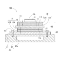
- a power module 100 with a heat sink shown in FIG. 1 includes a power module substrate 20 with a heat sink and a semiconductor element 30 bonded to the power module substrate 20 with a heat sink.
- the power module substrate 20 with a heat sink includes a power module substrate 10 and a heat sink 40 bonded to the power module substrate 10.
- the power module substrate 10 includes a ceramic substrate 11, a circuit layer 12 stacked on one surface 11f of the ceramic substrate 11, and a metal layer 13 stacked on the other surface 11b of the ceramic substrate 11. .
- the ceramic substrate 11 prevents electrical connection between the circuit layer 12 and the metal layer 13, and is made of AlN, Si 3 N 4 , Al 2 O 3 or the like.
- the thickness of the ceramic substrate 11 is set in a range of 0.2 mm to 1.5 mm, and in this embodiment is set to 0.635 mm.
- the circuit layer 12 includes a first aluminum layer 12A bonded to one surface 11f of the ceramic substrate 11, and a first copper layer 12B laminated on one side (the upper side in FIG. 1) of the first aluminum layer 12A. Have.
- the first aluminum layer 12 ⁇ / b> A is formed by joining a plate made of pure aluminum or an aluminum alloy to one surface 11 f of the ceramic substrate 11.
- the first aluminum layer 12A is made of a rolled plate of aluminum (so-called 4N aluminum) having a purity of 99.99% or more.
- the first copper layer 12B is formed by joining a plate made of pure copper or a copper alloy to one side (the upper side in FIG. 1) of the first aluminum layer 12A.
- the first copper layer 12B is formed by solid phase diffusion bonding of a copper plate made of an oxygen-free copper rolled plate to the first aluminum layer 12A.
- the metal layer 13 includes a second aluminum layer 13A joined to the other surface 11b of the ceramic substrate 11, and a second copper layer 13B laminated on the other side (lower side in FIG. 1) of the second aluminum layer 13A. have.
- the second aluminum layer 13A is formed by bonding an aluminum plate made of the same material as the first aluminum layer 12A of the circuit layer 12 to the other surface 11b of the ceramic substrate 11.
- the second aluminum layer 13A is also joined to the ceramic substrate 11 by an aluminum plate made of a rolled plate of aluminum (so-called 4N aluminum) having the same purity as the first aluminum layer 12A of 99.99% or more. It is formed by.
- the second copper layer 13B is formed of the same material as the first copper layer 12B of the circuit layer 12 and bonded to the other side (lower side in FIG. 1) of the second aluminum layer 13A. Therefore, in the present embodiment, the second copper layer 13B is formed by solid-phase diffusion bonding a copper plate made of the same oxygen-free copper rolled plate as the first copper layer 12B to the second aluminum layer 13A. .
- the thickness t1 of the first copper layer 12B of the circuit layer 12 of the power module substrate 10 thus configured is 1.7 mm or more and 5 mm or less.
- the total of the thickness t1 of the first copper layer 12B and the thickness t2 of the second copper layer 13B is 7 mm or less, and the ratio t2 between the thickness t1 of the first copper layer 12B and the thickness t2 of the second copper layer 13B.
- / T1 is set to a range excluding 0.6 or more and 0.8 or less in a range of more than 0 and 1.2 or less.
- the planar size of the circuit layer 12 and the metal layer 13 is smaller than the planar size of the rectangular ceramic substrate 11 having one side of 30 mm or more and 150 mm or less.
- the first aluminum layer 12A and the first copper layer 12B constituting the circuit layer 12 are bonded by solid phase diffusion bonding as described above, and an intermetallic compound is formed on these interfaces as shown in FIG. Layer 14 is formed.
- the intermetallic compound layer 14 is formed by interdiffusion of Al atoms in the first aluminum layer 12A and Cu atoms in the first copper layer 12B.
- the intermetallic compound layer 14 formed at the interface between the first aluminum layer 12A and the first copper layer 12B gradually decreases in concentration of Al atoms from the first aluminum layer 12A toward the first copper layer 12B. And it has a concentration gradient that increases the concentration of Cu atoms.
- the second aluminum layer 13A and the second copper layer 13B constituting the metal layer 13 are joined by solid phase diffusion bonding as described above, and at these interfaces, as shown in FIG.
- An intermetallic compound layer 14 is formed.
- the intermetallic compound layer 14 is formed by mutual diffusion of Al atoms in the second aluminum layer 13A and Cu atoms in the second copper layer 13B.
- the intermetallic compound layer 14 formed at the interface between the second aluminum layer 13A and the second copper layer 13B gradually decreases in the concentration of Al atoms from the second aluminum layer 13A toward the second copper layer 13B. And it has a concentration gradient that increases the concentration of Cu atoms.
- the intermetallic compound layer 14 formed of the intermetallic compound composed of Cu and Al has a structure in which a plurality of intermetallic compounds are stacked along the bonding interface.
- the thickness of the intermetallic compound layer 14 is set in the range of 1 ⁇ m to 80 ⁇ m, preferably in the range of 5 ⁇ m to 80 ⁇ m.
- the intermetallic compound layer 14 of the present embodiment has a structure in which three types of intermetallic compounds are laminated. That is, the first aluminum layer 12A (second aluminum layer 13A) and the first copper are sequentially arranged from the first aluminum layer 12A (second aluminum layer 13A) side to the first copper layer 12B (second copper layer 13B) side.
- the ⁇ phase 16 and the ⁇ 2 phase 17 are laminated along the bonding interface with the layer 12B (second copper layer 13B), and further includes at least one of the ⁇ 2 phase 18A, the ⁇ phase 18B, and the ⁇ 2 phase 18C. Phase 18 is laminated (FIG. 7).
- the oxide 19 has a ⁇ phase 16, a ⁇ 2 phase 17, or a ⁇ 2 phase 18A, a ⁇ phase 18B, And ⁇ 2 phase 18C are dispersed in layers within at least one of the phases.
- the oxide 19 is an aluminum oxide such as alumina (Al 2 O 3 ).
- the oxide 19 may be disperse
- the heat sink 40 dissipates heat on the power module substrate 10 side.
- the heat sink 40 of this embodiment includes a heat radiating plate 41 to which the power module substrate 10 is joined and a cooling part 42 provided with a flow path 42a for circulating a cooling medium (for example, cooling water).
- the plate 41 and the cooling unit 42 are fixed by screws 43 via grease (not shown).
- the heat sink 40 is preferably made of a material having good thermal conductivity.
- the heat radiating plate 41 is made of oxygen-free copper
- the cooling part 42 is made of an aluminum alloy.
- the heat sink 41 of the heat sink 40 and the second copper layer 13 ⁇ / b> B of the metal layer 13 are joined by the solder layer 45.
- the solder layer 45 is, for example, a Sn—Sb, Sn—Ag, Sn—Cu, Sn—In, or Sn—Ag—Cu solder material (so-called lead-free solder material).
- the semiconductor element 30 is an electronic component including a semiconductor, and various semiconductor elements are selected according to a required function.
- the semiconductor element 30 is bonded to the first copper layer 12 ⁇ / b> B of the circuit layer 12 through the solder layer 31.
- the solder layer 31 is a solder material (so-called lead-free solder material) such as Sn—Ag, Sn—Cu, Sn—In, or Sn—Ag—Cu.
- aluminum is provided on both surfaces of the ceramic substrate 11 (one surface 11f and the other surface 11b in the present invention) via an Al—Si based brazing material (not shown).
- the plates 12a and 13a are stacked.
- the ceramic substrate 11 and the aluminum plates 12a and 13a are joined, and the first aluminum layer 12A and the second aluminum layer 13A are joined to the ceramic substrate 11 as shown in FIG. Is formed (aluminum layer forming step S11).
- This brazing temperature is set to 610 ° C to 650 ° C.
- the copper plate 12b is disposed on one side (upper side) of the first aluminum layer 12A, and the copper plate 13b is disposed on the other side (lower side) of the second aluminum layer 13A.
- this laminated body is inserted in the vacuum heating furnace 50 in the state pressurized to the lamination direction, and heat processing is performed.
- the load applied to the contact surface of the first aluminum layer 12A and the copper plate 12b, the contact surface of the second aluminum layer 13A and the copper plate 13b is 0.29 MPa or more and 3.43 MPa or less, and the heating temperature is 400 ° C. or more. Solid phase diffusion bonding is performed at a temperature lower than 548 ° C. and maintained for 5 minutes to 240 minutes.
- the copper plate 12b is joined to the first aluminum layer 12A to form the first copper layer 12B, and at the same time, the copper plate 13b is joined to the second aluminum layer 13A. 13B is formed (copper layer forming step S12). Thereby, the circuit layer 12 and the metal layer 13 are formed, and the power module substrate 10 according to the present embodiment is obtained (FIG. 4A).
- the joining surface between the first aluminum layer 12A and the copper plate 12b and the joining surface between the second aluminum layer 13A and the copper plate 13b are previously solidified by removing scratches and then solid-phase diffusion bonded. Is done.
- the preferable heating temperature for vacuum heating in solid phase diffusion bonding is in the range of eutectic temperature of Al and Cu of ⁇ 5 ° C. or higher and lower than the eutectic temperature.
- the heat sink 40 is bonded to the other side (lower side) of the power module substrate 10 (heat sink bonding step S13).
- the heat sink joining step S13 as shown in FIG. 4 (b), after the heat sink 41 is soldered to the other side of the power module substrate 10 by the solder layer 45, the heat sink 41 is shown in FIG.
- the heat sink 40 is joined to the power module substrate 10 by disposing the cooling unit 42 via grease as shown in FIG. In this way, the power module substrate 20 with a heat sink is obtained.
- step S14 the power module with heat sink 100 according to the present embodiment is obtained.
- a manufacturing flow of the power module 100 with the heat sink is shown in FIG.
- the circuit layer 12 is bonded to the one surface 11f of the ceramic substrate 11. Since the first aluminum layer 12A and the first copper layer 12B joined to the first aluminum layer 12A are formed, and the semiconductor element 30 is mounted on the first copper layer 12B, the semiconductor element 30 The generated heat can be efficiently dissipated by spreading in the surface direction with the first copper layer 12B.
- the first aluminum layer 12A having a relatively small deformation resistance is joined between the ceramic substrate 11 and the first copper layer 12B, the ceramic substrate 11 and the circuit layer 12 (the first layer) when the thermal cycle is applied. It is possible to prevent the first aluminum layer 12A from absorbing the thermal stress generated due to the difference in thermal expansion coefficient from the one copper layer 12B) and causing the ceramic substrate 11 to crack. Further, the first copper layer 12B having a relatively large deformation resistance joined to the first aluminum layer 12A can suppress the deformation of the circuit layer 12 when a power cycle is applied. It can suppress that a crack arises in solder layer 31 which joins.
- first aluminum layer 12A and the first copper layer 12B are bonded by solid phase diffusion bonding, when a cooling cycle is applied, the first aluminum layer 12A and the first copper layer 12B are interposed between the first aluminum layer 12A and the first copper layer 12B. The occurrence of peeling is suppressed, and the thermal conductivity and conductivity of the circuit layer 12 can be maintained well.
- the thickness t1 of the first copper layer 12B is set to 1.7 mm or more and 5 mm or less. This is because if the thickness t1 is less than 1.7 mm, it is difficult to spread the heat from the semiconductor element 30 in the plane direction, and thus the thermal resistance during power cycle load cannot be sufficiently reduced, and the reliability with respect to the power cycle is ensured. Because it becomes difficult. In addition, in the range where the thickness t1 exceeds 5 mm, there is no significant difference in heat dissipation performance, so the thickness t1 is set to 5 mm or less from the viewpoint of miniaturization of the entire power module.
- the total of the thickness t1 of the first copper layer 12B and the thickness t2 of the second copper layer 13B is 7 mm or less.
- the lower limit of the total thickness t1 of the first copper layer 12B and the thickness t2 of the second copper layer 13B is not particularly limited, but is preferably 3.4 mm or more.
- the metal layer 13 is formed of the second aluminum layer 13A bonded to the other surface 11b of the ceramic substrate 11 and the second copper layer 13B bonded to the second aluminum layer 13A.
- the metal layer 13 and the heat sink 40 can be satisfactorily bonded without forming plating. Further, since the deformation resistance of the second copper layer 13B joined to the heat sink 40 via the solder layer 45 is relatively high, cracks in the solder layer 45 caused by the deformation of the metal layer 13 when a cooling cycle is applied. It is possible to suppress a decrease in bonding reliability and an increase in thermal resistance.
- the second aluminum layer 13A having a relatively small deformation resistance is joined to the second copper layer 13B, the thermal stress generated between the ceramic substrate 11 and the second copper layer 13B is maintained even when a cooling cycle is applied. Absorption by the second aluminum layer 13A can prevent the ceramic substrate 11 from cracking.
- the second aluminum layer 13A and the second copper layer 13B are joined by solid phase diffusion bonding, even when a cooling cycle is applied, the second aluminum layer 13A and the second copper layer 13B are disposed between the second aluminum layer 13A and the second copper layer 13B. Is suppressed, and the thermal conductivity of the metal layer 13 can be maintained well.
- the ratio t2 / t1 between the thickness t1 of the first copper layer 12B and the thickness t2 of the second copper layer 13B exceeds 0 and falls within the range of 1.2 or less, but the range excluding 0.6 or more and 0.8 or less (that is, 0 And less than 0.6 and more than 0.8 and 1.2 or less).
- the thickness t1 of the first copper layer 12B and the thickness t2 of the second copper layer 13B are relatively close, so the warpage of the entire power module substrate 10 is Although it becomes small, the rigidity of the 2nd copper layer 13B provided comparatively thick with respect to the 1st copper layer 12B is high, and the curvature of the opposite direction by the 1st copper layer 12B and the 2nd copper layer 13B which arises at the time of a thermal cycle is produced. Loaded on the ceramic substrate 11. As a result, the load applied to the ceramic substrate 11 becomes large and the ceramic substrate 11 may be cracked although the amount of warpage generated in the entire power module substrate 10 is small.
- the thickness t2 of the second copper layer 13B is smaller than the thickness t1 of the first copper layer 12B, and the rigidity of the second copper layer 13B is relatively low.
- the warp of the power module substrate 10 generated during the cooling / heating cycle is increased due to the thermal expansion / contraction difference between the copper layer 12B and the second copper layer 13B, the second copper layer 13B deforms following the first copper layer 12B. The stress generated in the ceramic substrate 11 can be reduced, and the ceramic substrate 11 can be prevented from cracking.
- the thickness t1 of the first copper layer 12B and the thickness t2 of the second copper layer 13B are substantially the same. The balance between the warp generated and the warp generated in the second copper layer 13B is maintained, warp generated in the power module substrate 10 can be reduced, and cracking of the ceramic substrate 11 can be suppressed.
- the heat sink 40 is made of oxygen-free copper
- it can be made of pure copper such as tough pitch copper or a copper alloy.
- the heat sink can also be made of aluminum or an aluminum alloy.
- the power module substrate and the heat sink can be satisfactorily bonded to each other by soldering the heat sink with Ni plating.
- the joining of the heat radiation plate 41 and the cooling part 42 of the heat sink 40 is not limited to fixing with screws, and may be joined by, for example, solid phase diffusion joining.
- the heat sink 40 can be configured without using the heat radiating plate 41 to directly bond the power module substrate 10 and the cooling unit 42.
- the heat sink can employ various configurations such as a heat pipe that dissipate heat.
- first aluminum layer 12A and the first copper layer 12B, and the second aluminum layer 13A and the second copper layer 13B are simultaneously solid-phase diffusion bonded. Phase diffusion bonding may be performed.
- the first aluminum layer 12A and the second aluminum layer 13A are not limited to pure aluminum having a purity of 99.99%, and may be 99% pure aluminum (so-called 2N aluminum), an aluminum alloy, or the like.
- a power module substrate was used in which a circuit layer and a metal layer were laminated on a ceramic substrate made of the material described in Table 1 with a thickness of 40 mm ⁇ 40 mm and a thickness of 0.635 mm.
- the first aluminum layer of the circuit layer and the second aluminum layer of the metal layer are each formed by joining the aluminum plate shown in Table 1 with a thickness of 37 mm ⁇ 37 mm and a thickness of 0.6 mm to the ceramic substrate with an Al—Si brazing material. did.
- the first copper layer of the circuit layer and the second copper layer of the metal layer are formed by solid phase diffusion bonding of the copper plate described in Table 1 to the first aluminum layer and the second aluminum layer, respectively 37 mm ⁇ 37 mm, A power module substrate was manufactured as a sample for each example. Solid phase diffusion bonding was performed at a pressure in the vacuum heating furnace of 1.0 ⁇ 10 ⁇ 6 Pa to 1.0 ⁇ 10 ⁇ 3 Pa.
- the thermal cycle test uses a thermal shock tester TSB-51 manufactured by Espec Co., Ltd., and is -40 ° C. in liquid phase (fluorine-based inert liquid (3M Fluorinert)) for each power module substrate. 3000 cycles of 5 minutes and 125 ° C. ⁇ 5 minutes were repeated.
- Example 13 the power module substrate of Invention Example 5 was used.
- Inventive Example 14 the power module substrate of Inventive Example 7 was used.
- Inventive Example 15 the power module substrate of Inventive Example 10 was used.
- Invention Example 16 the power module substrate of Invention Example 12 was used.
- Inventive Example 13 and Inventive Example 16 used heat sinks made of Al alloy (A6063) plated with Ni, and Inventive Examples 14 and 15 used heat sinks made of oxygen-free copper.
- the obtained power module substrate with a heat sink was evaluated for the bonding rate between the second copper layer and the solder layer interface before and after the thermal cycle test, and the ceramic crack after the thermal cycle test.
- the initial bonding area is the area to be bonded before bonding, that is, the area of the second copper layer in this example.
- the area of the white portion is defined as the peeled area.
- the thickness t1 of the first copper layer is set to 1.7 mm or more and 5 mm or less, and the ratio t2 / t1 exceeds 0 and excludes 0.6 or more and 0.8 or less in the range of 1.2 or less.
- the ceramic substrate after the thermal cycle test was not cracked. A power module substrate could be obtained.
- Comparative Example 4 in which the ratio t2 / t1 exceeded 1.2 as shown in the ultrasonic image of FIG. 6, the ceramic substrate after the thermal cycle test was cracked.
- radial streaks were confirmed, and cracks were generated in the thickness direction of the ceramic substrate. Further, in addition to the radial streaks, local white scattered areas were observed, and it was found that cracks were also generated in the horizontal direction of the ceramic substrate.
Landscapes
- Engineering & Computer Science (AREA)
- Chemical & Material Sciences (AREA)
- Ceramic Engineering (AREA)
- Materials Engineering (AREA)
- Mechanical Engineering (AREA)
- Structural Engineering (AREA)
- Organic Chemistry (AREA)
- Cooling Or The Like Of Semiconductors Or Solid State Devices (AREA)
Abstract
Priority Applications (4)
| Application Number | Priority Date | Filing Date | Title |
|---|---|---|---|
| CN201580018737.9A CN106165087B (zh) | 2014-04-25 | 2015-04-24 | 功率模块用基板、带散热片的功率模块用基板及带散热片的功率模块 |
| US15/305,689 US9786577B2 (en) | 2014-04-25 | 2015-04-24 | Power module substrate, heat-sink-attached power-module substrate, and heat-sink-attached power module |
| EP15783462.3A EP3136431B1 (fr) | 2014-04-25 | 2015-04-24 | Substrat pour modules de puissance, substrat ayant un dissipateur thermique pour modules de puissance, et module de puissance ayant un dissipateur thermique |
| KR1020167031383A KR102271651B1 (ko) | 2014-04-25 | 2015-04-24 | 파워 모듈용 기판 및 히트 싱크가 부착된 파워 모듈용 기판 그리고 히트 싱크가 부착된 파워 모듈 |
Applications Claiming Priority (2)
| Application Number | Priority Date | Filing Date | Title |
|---|---|---|---|
| JP2014091814A JP6384112B2 (ja) | 2014-04-25 | 2014-04-25 | パワーモジュール用基板及びヒートシンク付パワーモジュール用基板 |
| JP2014-091814 | 2014-04-25 |
Publications (1)
| Publication Number | Publication Date |
|---|---|
| WO2015163452A1 true WO2015163452A1 (fr) | 2015-10-29 |
Family
ID=54332612
Family Applications (1)
| Application Number | Title | Priority Date | Filing Date |
|---|---|---|---|
| PCT/JP2015/062544 Ceased WO2015163452A1 (fr) | 2014-04-25 | 2015-04-24 | Substrat pour modules de puissance, substrat ayant un dissipateur thermique pour modules de puissance, et module de puissance ayant un dissipateur thermique |
Country Status (7)
| Country | Link |
|---|---|
| US (1) | US9786577B2 (fr) |
| EP (1) | EP3136431B1 (fr) |
| JP (1) | JP6384112B2 (fr) |
| KR (1) | KR102271651B1 (fr) |
| CN (1) | CN106165087B (fr) |
| TW (1) | TWI646638B (fr) |
| WO (1) | WO2015163452A1 (fr) |
Cited By (2)
| Publication number | Priority date | Publication date | Assignee | Title |
|---|---|---|---|---|
| US20220009022A1 (en) * | 2018-12-21 | 2022-01-13 | Nhk Spring Co., Ltd. | Joining method and joined body |
| US20220055133A1 (en) * | 2017-05-10 | 2022-02-24 | Board Of Trustees Of Michigan State University | Brazing methods using porous interlayers and related articles |
Families Citing this family (22)
| Publication number | Priority date | Publication date | Assignee | Title |
|---|---|---|---|---|
| JP6811551B2 (ja) * | 2016-05-27 | 2021-01-13 | 日産自動車株式会社 | 電力変換装置の製造方法と冷却構造 |
| JP6645396B2 (ja) * | 2016-10-07 | 2020-02-14 | 株式会社デンソー | 半導体装置 |
| KR102709152B1 (ko) * | 2016-11-10 | 2024-09-25 | 주식회사 아모센스 | 세라믹 기판 제조 방법 |
| US10178813B2 (en) * | 2017-01-26 | 2019-01-08 | The United States Of America As Represented By The Secretary Of The Army | Stacked power module with integrated thermal management |
| JP6776953B2 (ja) * | 2017-03-07 | 2020-10-28 | 三菱マテリアル株式会社 | ヒートシンク付パワーモジュール用基板 |
| JP6717238B2 (ja) * | 2017-03-07 | 2020-07-01 | 三菱マテリアル株式会社 | ヒートシンク付パワーモジュール用基板 |
| JP7125931B2 (ja) * | 2017-03-31 | 2022-08-25 | ローム株式会社 | パワーモジュールおよびその製造方法 |
| DE102017205813A1 (de) * | 2017-04-05 | 2018-10-11 | Mahle International Gmbh | Verfahren zum Herstellen einer Kühlvorrichtung, eine Kühlvorrichtung und eine Kühlanordnung |
| CN109309066B (zh) * | 2017-07-27 | 2020-10-20 | 比亚迪股份有限公司 | 一种陶瓷覆铝铜板及其制备方法、散热元件和igbt模组 |
| US11094648B2 (en) * | 2017-08-04 | 2021-08-17 | Denka Company Limited | Power module |
| JP7027095B2 (ja) * | 2017-09-28 | 2022-03-01 | デンカ株式会社 | セラミックス回路基板 |
| JP6601512B2 (ja) * | 2018-01-24 | 2019-11-06 | 三菱マテリアル株式会社 | ヒートシンク付きパワーモジュール用基板及びパワーモジュール |
| JP6614256B2 (ja) * | 2018-03-02 | 2019-12-04 | 三菱マテリアル株式会社 | 絶縁回路基板 |
| CN111819682B (zh) | 2018-03-26 | 2025-04-29 | 三菱综合材料株式会社 | 绝缘电路基板用接合体的制造方法及绝缘电路基板用接合体 |
| WO2019188884A1 (fr) * | 2018-03-27 | 2019-10-03 | 三菱マテリアル株式会社 | Carte de circuit imprimé avec dissipateur thermique |
| US11322424B2 (en) * | 2018-03-28 | 2022-05-03 | Mitsubishi Materials Corporation | Insulation circuit board with heat sink |
| DE112018007723T5 (de) * | 2018-06-12 | 2021-02-25 | Mitsubishi Electric Corporation | Leistungshalbleitermodul und leistungswandlervorrichtung |
| JP7238353B2 (ja) * | 2018-11-15 | 2023-03-14 | 富士電機株式会社 | 半導体モジュールおよびそれを用いた半導体装置 |
| WO2020131360A1 (fr) * | 2018-12-17 | 2020-06-25 | Heraeus Precious Metals North America Conshohocken Llc | Procédé de formation d'un dispositif de chauffage électrique |
| JP7524545B2 (ja) * | 2020-01-27 | 2024-07-30 | 三菱マテリアル株式会社 | ヒートシンク付き絶縁回路基板 |
| CN117352470A (zh) * | 2020-03-27 | 2024-01-05 | 瑷司柏电子股份有限公司 | 具有保护接垫的高导热陶瓷基板及具该基板的大功率模块 |
| JP7350369B2 (ja) * | 2020-03-27 | 2023-09-26 | 富山県 | 金属材料の接合方法 |
Citations (4)
| Publication number | Priority date | Publication date | Assignee | Title |
|---|---|---|---|---|
| JPH11195854A (ja) * | 1997-11-07 | 1999-07-21 | Denki Kagaku Kogyo Kk | 基板とその製造法、基板に好適な金属接合体 |
| JP2003078086A (ja) * | 2001-09-04 | 2003-03-14 | Kubota Corp | 半導体素子モジュール基板の積層構造 |
| JP2006202884A (ja) * | 2005-01-19 | 2006-08-03 | Fuji Electric Device Technology Co Ltd | 半導体装置およびその製造方法 |
| JP2014039062A (ja) * | 2012-03-30 | 2014-02-27 | Mitsubishi Materials Corp | パワーモジュール用基板、ヒートシンク付パワーモジュール用基板、パワーモジュール、及びパワーモジュール用基板の製造方法 |
Family Cites Families (15)
| Publication number | Priority date | Publication date | Assignee | Title |
|---|---|---|---|---|
| JPH0435052A (ja) * | 1990-05-31 | 1992-02-05 | Ngk Spark Plug Co Ltd | 回路基板の製造方法 |
| US5156923A (en) * | 1992-01-06 | 1992-10-20 | Texas Instruments Incorporated | Heat-transferring circuit substrate with limited thermal expansion and method for making |
| JP4077888B2 (ja) * | 1995-07-21 | 2008-04-23 | 株式会社東芝 | セラミックス回路基板 |
| US6197435B1 (en) | 1997-11-07 | 2001-03-06 | Denki Kagaku Kogyo Kabushiki Kaisha | Substrate |
| US5895974A (en) * | 1998-04-06 | 1999-04-20 | Delco Electronics Corp. | Durable substrate subassembly for transistor switch module |
| JP2002203932A (ja) * | 2000-10-31 | 2002-07-19 | Hitachi Ltd | 半導体パワー素子用放熱基板とその導体板及びヒートシンク材並びにロー材 |
| JP2002158328A (ja) * | 2000-11-17 | 2002-05-31 | Mitsubishi Electric Corp | 電力用半導体装置 |
| CN1331217C (zh) * | 2003-11-10 | 2007-08-08 | 乾坤科技股份有限公司 | 晶片封装结构及其基板 |
| CN101971329B (zh) * | 2008-03-17 | 2012-11-21 | 三菱综合材料株式会社 | 带散热片的功率模块用基板及其制造方法、以及带散热片的功率模块、功率模块用基板 |
| CN101733982A (zh) * | 2009-12-18 | 2010-06-16 | 吉林大学 | 泡沫铝基复合材料层合板及其制备方法 |
| KR101204191B1 (ko) * | 2010-11-02 | 2012-11-23 | 삼성전기주식회사 | 방열기판 |
| JP5403129B2 (ja) * | 2012-03-30 | 2014-01-29 | 三菱マテリアル株式会社 | パワーモジュール用基板、ヒートシンク付パワーモジュール用基板、パワーモジュール、及びパワーモジュール用基板の製造方法 |
| JP2013229579A (ja) | 2012-03-30 | 2013-11-07 | Mitsubishi Materials Corp | パワーモジュール用基板、ヒートシンク付パワーモジュール用基板及びパワーモジュール |
| JP5991103B2 (ja) * | 2012-09-14 | 2016-09-14 | 三菱マテリアル株式会社 | ヒートシンク付パワーモジュール用基板、ヒートシンク付パワーモジュール、及びヒートシンク付パワーモジュール用基板の製造方法 |
| JP6621076B2 (ja) * | 2013-03-29 | 2019-12-18 | 三菱マテリアル株式会社 | パワーモジュール用基板、ヒートシンク付パワーモジュール用基板及びパワーモジュール |
-
2014
- 2014-04-25 JP JP2014091814A patent/JP6384112B2/ja active Active
-
2015
- 2015-04-24 TW TW104113264A patent/TWI646638B/zh not_active IP Right Cessation
- 2015-04-24 US US15/305,689 patent/US9786577B2/en active Active
- 2015-04-24 EP EP15783462.3A patent/EP3136431B1/fr active Active
- 2015-04-24 CN CN201580018737.9A patent/CN106165087B/zh active Active
- 2015-04-24 WO PCT/JP2015/062544 patent/WO2015163452A1/fr not_active Ceased
- 2015-04-24 KR KR1020167031383A patent/KR102271651B1/ko not_active Expired - Fee Related
Patent Citations (4)
| Publication number | Priority date | Publication date | Assignee | Title |
|---|---|---|---|---|
| JPH11195854A (ja) * | 1997-11-07 | 1999-07-21 | Denki Kagaku Kogyo Kk | 基板とその製造法、基板に好適な金属接合体 |
| JP2003078086A (ja) * | 2001-09-04 | 2003-03-14 | Kubota Corp | 半導体素子モジュール基板の積層構造 |
| JP2006202884A (ja) * | 2005-01-19 | 2006-08-03 | Fuji Electric Device Technology Co Ltd | 半導体装置およびその製造方法 |
| JP2014039062A (ja) * | 2012-03-30 | 2014-02-27 | Mitsubishi Materials Corp | パワーモジュール用基板、ヒートシンク付パワーモジュール用基板、パワーモジュール、及びパワーモジュール用基板の製造方法 |
Cited By (3)
| Publication number | Priority date | Publication date | Assignee | Title |
|---|---|---|---|---|
| US20220055133A1 (en) * | 2017-05-10 | 2022-02-24 | Board Of Trustees Of Michigan State University | Brazing methods using porous interlayers and related articles |
| US11724325B2 (en) * | 2017-05-10 | 2023-08-15 | Board Of Trustees Of Michigan State University | Brazing methods using porous interlayers and related articles |
| US20220009022A1 (en) * | 2018-12-21 | 2022-01-13 | Nhk Spring Co., Ltd. | Joining method and joined body |
Also Published As
| Publication number | Publication date |
|---|---|
| CN106165087A (zh) | 2016-11-23 |
| US20170047268A1 (en) | 2017-02-16 |
| CN106165087B (zh) | 2020-08-25 |
| TW201613037A (en) | 2016-04-01 |
| EP3136431A1 (fr) | 2017-03-01 |
| JP2015211125A (ja) | 2015-11-24 |
| JP6384112B2 (ja) | 2018-09-05 |
| US9786577B2 (en) | 2017-10-10 |
| KR20160146799A (ko) | 2016-12-21 |
| EP3136431A4 (fr) | 2017-12-20 |
| EP3136431B1 (fr) | 2020-12-16 |
| TWI646638B (zh) | 2019-01-01 |
| KR102271651B1 (ko) | 2021-06-30 |
Similar Documents
| Publication | Publication Date | Title |
|---|---|---|
| JP6384112B2 (ja) | パワーモジュール用基板及びヒートシンク付パワーモジュール用基板 | |
| CN104919585B (zh) | 功率模块用基板、自带散热器的功率模块用基板、自带散热器的功率模块 | |
| KR102146589B1 (ko) | 히트싱크가 부착된 파워 모듈용 기판, 히트싱크가 부착된 파워 모듈, 및 히트싱크가 부착된 파워 모듈용 기판의 제조 방법 | |
| TWI620289B (zh) | 附散熱座功率模組用基板,附冷卻器功率模組用基板及功率模組 | |
| KR101971756B1 (ko) | 파워 모듈용 기판, 히트 싱크 부착 파워 모듈용 기판, 파워 모듈 및 파워 모듈용 기판의 제조 방법 | |
| CN105009278B (zh) | 功率模块用基板、自带散热器的功率模块用基板及功率模块 | |
| KR102097177B1 (ko) | 파워 모듈용 기판, 히트싱크가 부착된 파워 모듈용 기판 및 파워 모듈 | |
| JP2013229579A5 (fr) | ||
| KR102154882B1 (ko) | 파워 모듈 | |
| JP2013065918A5 (fr) | ||
| CN105393348A (zh) | 接合体及功率模块用基板 | |
| JP5966512B2 (ja) | ヒートシンク付パワーモジュール用基板の製造方法 |
Legal Events
| Date | Code | Title | Description |
|---|---|---|---|
| 121 | Ep: the epo has been informed by wipo that ep was designated in this application |
Ref document number: 15783462 Country of ref document: EP Kind code of ref document: A1 |
|
| WWE | Wipo information: entry into national phase |
Ref document number: 15305689 Country of ref document: US |
|
| NENP | Non-entry into the national phase |
Ref country code: DE |
|
| REEP | Request for entry into the european phase |
Ref document number: 2015783462 Country of ref document: EP |
|
| WWE | Wipo information: entry into national phase |
Ref document number: 2015783462 Country of ref document: EP |
|
| ENP | Entry into the national phase |
Ref document number: 20167031383 Country of ref document: KR Kind code of ref document: A |