WO2015166754A1 - Dispositif à semi-conducteur - Google Patents
Dispositif à semi-conducteur Download PDFInfo
- Publication number
- WO2015166754A1 WO2015166754A1 PCT/JP2015/059968 JP2015059968W WO2015166754A1 WO 2015166754 A1 WO2015166754 A1 WO 2015166754A1 JP 2015059968 W JP2015059968 W JP 2015059968W WO 2015166754 A1 WO2015166754 A1 WO 2015166754A1
- Authority
- WO
- WIPO (PCT)
- Prior art keywords
- cell
- region
- semiconductor device
- base region
- trench
- Prior art date
- Legal status (The legal status is an assumption and is not a legal conclusion. Google has not performed a legal analysis and makes no representation as to the accuracy of the status listed.)
- Ceased
Links
Images


Classifications
-
- H—ELECTRICITY
- H10—SEMICONDUCTOR DEVICES; ELECTRIC SOLID-STATE DEVICES NOT OTHERWISE PROVIDED FOR
- H10D—INORGANIC ELECTRIC SEMICONDUCTOR DEVICES
- H10D62/00—Semiconductor bodies, or regions thereof, of devices having potential barriers
- H10D62/10—Shapes, relative sizes or dispositions of the regions of the semiconductor bodies; Shapes of the semiconductor bodies
- H10D62/124—Shapes, relative sizes or dispositions of the regions of semiconductor bodies or of junctions between the regions
- H10D62/126—Top-view geometrical layouts of the regions or the junctions
- H10D62/127—Top-view geometrical layouts of the regions or the junctions of cellular field-effect devices, e.g. multicellular DMOS transistors or IGBTs
-
- H—ELECTRICITY
- H10—SEMICONDUCTOR DEVICES; ELECTRIC SOLID-STATE DEVICES NOT OTHERWISE PROVIDED FOR
- H10D—INORGANIC ELECTRIC SEMICONDUCTOR DEVICES
- H10D12/00—Bipolar devices controlled by the field effect, e.g. insulated-gate bipolar transistors [IGBT]
- H10D12/411—Insulated-gate bipolar transistors [IGBT]
- H10D12/441—Vertical IGBTs
- H10D12/461—Vertical IGBTs having non-planar surfaces, e.g. having trenches, recesses or pillars in the surfaces of the emitter, base or collector regions
- H10D12/481—Vertical IGBTs having non-planar surfaces, e.g. having trenches, recesses or pillars in the surfaces of the emitter, base or collector regions having gate structures on slanted surfaces, on vertical surfaces, or in grooves, e.g. trench gate IGBTs
-
- H—ELECTRICITY
- H10—SEMICONDUCTOR DEVICES; ELECTRIC SOLID-STATE DEVICES NOT OTHERWISE PROVIDED FOR
- H10D—INORGANIC ELECTRIC SEMICONDUCTOR DEVICES
- H10D30/00—Field-effect transistors [FET]
- H10D30/60—Insulated-gate field-effect transistors [IGFET]
- H10D30/64—Double-diffused metal-oxide semiconductor [DMOS] FETs
- H10D30/66—Vertical DMOS [VDMOS] FETs
- H10D30/668—Vertical DMOS [VDMOS] FETs having trench gate electrodes, e.g. UMOS transistors
-
- H—ELECTRICITY
- H10—SEMICONDUCTOR DEVICES; ELECTRIC SOLID-STATE DEVICES NOT OTHERWISE PROVIDED FOR
- H10D—INORGANIC ELECTRIC SEMICONDUCTOR DEVICES
- H10D62/00—Semiconductor bodies, or regions thereof, of devices having potential barriers
- H10D62/10—Shapes, relative sizes or dispositions of the regions of the semiconductor bodies; Shapes of the semiconductor bodies
- H10D62/102—Constructional design considerations for preventing surface leakage or controlling electric field concentration
- H10D62/103—Constructional design considerations for preventing surface leakage or controlling electric field concentration for increasing or controlling the breakdown voltage of reverse-biased devices
- H10D62/105—Constructional design considerations for preventing surface leakage or controlling electric field concentration for increasing or controlling the breakdown voltage of reverse-biased devices by having particular doping profiles, shapes or arrangements of PN junctions; by having supplementary regions, e.g. junction termination extension [JTE]
- H10D62/106—Constructional design considerations for preventing surface leakage or controlling electric field concentration for increasing or controlling the breakdown voltage of reverse-biased devices by having particular doping profiles, shapes or arrangements of PN junctions; by having supplementary regions, e.g. junction termination extension [JTE] having supplementary regions doped oppositely to or in rectifying contact with regions of the semiconductor bodies, e.g. guard rings with PN or Schottky junctions
- H10D62/107—Buried supplementary regions, e.g. buried guard rings
-
- H—ELECTRICITY
- H10—SEMICONDUCTOR DEVICES; ELECTRIC SOLID-STATE DEVICES NOT OTHERWISE PROVIDED FOR
- H10D—INORGANIC ELECTRIC SEMICONDUCTOR DEVICES
- H10D62/00—Semiconductor bodies, or regions thereof, of devices having potential barriers
- H10D62/10—Shapes, relative sizes or dispositions of the regions of the semiconductor bodies; Shapes of the semiconductor bodies
- H10D62/13—Semiconductor regions connected to electrodes carrying current to be rectified, amplified or switched, e.g. source or drain regions
- H10D62/149—Source or drain regions of field-effect devices
- H10D62/151—Source or drain regions of field-effect devices of IGFETs
- H10D62/152—Source regions of DMOS transistors
- H10D62/154—Dispositions
-
- H—ELECTRICITY
- H10—SEMICONDUCTOR DEVICES; ELECTRIC SOLID-STATE DEVICES NOT OTHERWISE PROVIDED FOR
- H10D—INORGANIC ELECTRIC SEMICONDUCTOR DEVICES
- H10D62/00—Semiconductor bodies, or regions thereof, of devices having potential barriers
- H10D62/10—Shapes, relative sizes or dispositions of the regions of the semiconductor bodies; Shapes of the semiconductor bodies
- H10D62/13—Semiconductor regions connected to electrodes carrying current to be rectified, amplified or switched, e.g. source or drain regions
- H10D62/149—Source or drain regions of field-effect devices
- H10D62/151—Source or drain regions of field-effect devices of IGFETs
- H10D62/152—Source regions of DMOS transistors
- H10D62/155—Shapes
-
- H—ELECTRICITY
- H10—SEMICONDUCTOR DEVICES; ELECTRIC SOLID-STATE DEVICES NOT OTHERWISE PROVIDED FOR
- H10D—INORGANIC ELECTRIC SEMICONDUCTOR DEVICES
- H10D62/00—Semiconductor bodies, or regions thereof, of devices having potential barriers
- H10D62/80—Semiconductor bodies, or regions thereof, of devices having potential barriers characterised by the materials
- H10D62/83—Semiconductor bodies, or regions thereof, of devices having potential barriers characterised by the materials being Group IV materials, e.g. B-doped Si or undoped Ge
- H10D62/832—Semiconductor bodies, or regions thereof, of devices having potential barriers characterised by the materials being Group IV materials, e.g. B-doped Si or undoped Ge being Group IV materials comprising two or more elements, e.g. SiGe
- H10D62/8325—Silicon carbide
-
- H—ELECTRICITY
- H10—SEMICONDUCTOR DEVICES; ELECTRIC SOLID-STATE DEVICES NOT OTHERWISE PROVIDED FOR
- H10D—INORGANIC ELECTRIC SEMICONDUCTOR DEVICES
- H10D64/00—Electrodes of devices having potential barriers
- H10D64/20—Electrodes characterised by their shapes, relative sizes or dispositions
- H10D64/23—Electrodes carrying the current to be rectified, amplified, oscillated or switched, e.g. sources, drains, anodes or cathodes
- H10D64/251—Source or drain electrodes for field-effect devices
- H10D64/252—Source or drain electrodes for field-effect devices for vertical or pseudo-vertical devices
-
- H—ELECTRICITY
- H10—SEMICONDUCTOR DEVICES; ELECTRIC SOLID-STATE DEVICES NOT OTHERWISE PROVIDED FOR
- H10D—INORGANIC ELECTRIC SEMICONDUCTOR DEVICES
- H10D64/00—Electrodes of devices having potential barriers
- H10D64/20—Electrodes characterised by their shapes, relative sizes or dispositions
- H10D64/27—Electrodes not carrying the current to be rectified, amplified, oscillated or switched, e.g. gates
- H10D64/311—Gate electrodes for field-effect devices
- H10D64/411—Gate electrodes for field-effect devices for FETs
- H10D64/511—Gate electrodes for field-effect devices for FETs for IGFETs
- H10D64/512—Disposition of the gate electrodes, e.g. buried gates
- H10D64/513—Disposition of the gate electrodes, e.g. buried gates within recesses in the substrate, e.g. trench gates, groove gates or buried gates
-
- H—ELECTRICITY
- H10—SEMICONDUCTOR DEVICES; ELECTRIC SOLID-STATE DEVICES NOT OTHERWISE PROVIDED FOR
- H10D—INORGANIC ELECTRIC SEMICONDUCTOR DEVICES
- H10D64/00—Electrodes of devices having potential barriers
- H10D64/20—Electrodes characterised by their shapes, relative sizes or dispositions
- H10D64/27—Electrodes not carrying the current to be rectified, amplified, oscillated or switched, e.g. gates
- H10D64/311—Gate electrodes for field-effect devices
- H10D64/411—Gate electrodes for field-effect devices for FETs
- H10D64/511—Gate electrodes for field-effect devices for FETs for IGFETs
- H10D64/517—Gate electrodes for field-effect devices for FETs for IGFETs characterised by the conducting layers
- H10D64/519—Gate electrodes for field-effect devices for FETs for IGFETs characterised by the conducting layers characterised by their top-view geometrical layouts
Definitions
- the present invention relates to a trench gate type semiconductor device.
- Insulated gate semiconductor devices such as IGBTs (Insulated Gate Bipolar Transistors) and MOSFETs (Metal Oxide Semiconductor Semiconductor Field Field Effect Transistors) are widely used in power electronics equipment as switching elements that control power supply to motors and other loads.
- IGBTs Insulated Gate Bipolar Transistors
- MOSFETs Metal Oxide Semiconductor Semiconductor Field Field Effect Transistors
- power control MOSFETs the resistance during on-operation is small and the breakdown voltage during off-operation is required to be high.
- trench gate MOSFETs there is a trade-off between increasing the breakdown voltage and reducing the on-resistance. is there.
- MOSFETs and IGBTs using wide band gap semiconductors such as silicon carbide (SiC) are attracting attention as next-generation switching elements that can realize high breakdown voltage and low loss, and high voltages of about 1 kV or higher are attracting attention. It is considered promising for application in the technical field.
- a wide band gap semiconductor there are, for example, gallium nitride (GaN) -based material, diamond and the like in addition to SiC.
- MOSFETs for power control are handled as a single MOSFET by connecting a plurality of unit MOSFETs in parallel.
- MOSFETs can be classified according to the arrangement pattern of individual unit MOSFETs constituting the MOSFET.
- a source region is formed in a square pattern
- a cell type consisting of one unit MOSFET (cell) surrounded by a gate trench
- a source region is formed in an elongated stripe pattern
- the electric field is different from the inside of the MOSFET region at the outer periphery of the MOSFET region. For this reason, in a configuration in which cells having the same structure as the inside of the MOSFET region are arranged in the outer peripheral portion of the MOSFET region, avalanche breakdown may occur in the outer peripheral portion. Since the breakdown voltage of the entire MOSFET is determined by the lowest one of the breakdown voltages of the individual cells, the cells disposed in the outer peripheral portions having different electric field states are required to have a breakdown voltage equivalent to that of the internal cells. Therefore, for the purpose of increasing the breakdown voltage, it has been proposed that the cells arranged on the outer peripheral portion have a structure or dimensions different from those of the cells arranged inside.
- Patent Document 1 discloses a technique for suppressing the generation of a high electric field in the outer peripheral portion by extending a cell trench disposed in the outer peripheral portion to reach the electric field relaxation portion.
- Patent Document 2 discloses a technique for forming a structure dedicated to electric field relaxation in the outer peripheral portion, such as omitting the gate trench from all cells arranged in the outer peripheral portion. According to these techniques, the breakdown voltage in the outer peripheral cell where avalanche breakdown is likely to occur is improved, and the breakdown voltage of the entire MOSFET can be improved.
- the wiring for taking out the gate electrode and the source electrode of the MOSFET is connected to the gate pad and the source pad, respectively.
- the corners of the gate pad and the source pad may be formed in a curved shape. According to the analysis by the inventors, a tendency that avalanche breakdown frequently occurs in cells formed in a region facing the corner (curved portion) of the gate pad among the cells in the outer peripheral portion.
- Patent Documents 1 and 2 disclose a technique related to a cell in the outer peripheral portion, but suppress avalanche breakdown in a cell in which avalanche breakdown frequently occurs, that is, in a cell facing a corner (curved part) of the gate pad. That is not disclosed.
- the present invention has been made in view of the above problems, and an object thereof is to provide a technique capable of suppressing avalanche breakdown in a cell facing a corner of a gate pad.
- the semiconductor device includes a gate pad, a first cell disposed in a region facing a corner of the gate pad in plan view, and the gate pad opposite to the gate pad in plan view. 2nd cell arrange
- Each of the first and second cells includes a first conductive type semiconductor layer, a second conductive type base region formed on the semiconductor layer, and a lower portion of the base region through the base region.
- the trench reaching the semiconductor layer is disposed through a gate insulating film, and has a pattern corresponding to the outer shape of the first and second cells in plan view, and is electrically connected to the gate pad. Connected gate electrodes and a protective diffusion layer of the second conductivity type formed at the bottom of the trench.
- At least the second cell of the first and second cells includes a source region of a first conductivity type formed in a portion of the upper portion of the base region adjacent to the gate insulating film, the base region, and the base region.
- a source electrode electrically connected to the source region;
- the outline shape of the first and second cells is a quadrilateral or more polygonal shape, and each shortest distance between the longest side and each side facing the side in the outline shape of the first cell. Among these, the longest distance is equal to or less than twice the length of the equivalent one side or the short side of the second cell.
- the first cell disposed in a region facing the corner of the gate pad in plan view, and the second cell disposed in a region opposite to the gate pad with respect to the first cell,
- the longest distance is the length of an equal side or short side of the second cell. Less than twice. Therefore, avalanche breakdown in the first cell facing the corner portion of the gate pad can be suppressed.
- FIG. 3 is a plan view showing a configuration of a MOSFET according to the first embodiment.
- FIG. 3 is a plan view showing a configuration of a MOSFET according to the first embodiment.
- FIG. 3 is a plan view showing a configuration of a MOSFET according to the first embodiment.
- 3 is a cross-sectional view showing a configuration of a MOSFET according to the first embodiment.
- FIG. 3 is a cross-sectional view showing a configuration of a MOSFET according to the first embodiment.
- FIG. It is a top view which shows the structure of a part of related MOSFET. It is sectional drawing which shows the structure of a part of related MOSFET. It is a figure which shows the relationship between cell dimension ratio and electric field strength.
- FIG. 3 is a plan view showing a configuration of a MOSFET according to the first embodiment.
- 6 is a cross-sectional view showing the method of manufacturing the MOSFET according to the first embodiment.
- FIG. 6 is a cross-sectional view showing the method of manufacturing the MOSFET according to the first embodiment.
- FIG. 6 is a cross-sectional view showing the method of manufacturing the MOSFET according to the first embodiment.
- FIG. 6 is a cross-sectional view showing the method of manufacturing the MOSFET according to the first embodiment.
- FIG. 6 is a cross-sectional view showing the method of manufacturing the MOSFET according to the first embodiment.
- FIG. 6 is a cross-sectional view showing the method of manufacturing the MOSFET according to the first embodiment.
- FIG. 6 is a cross-sectional view showing the method of manufacturing the MOSFET according to the first embodiment.
- FIG. 6 is a cross-sectional view showing the method of manufacturing the MOSFET according to the first embodiment.
- FIG. FIG. 6 is a plan view showing a configuration of a MOSFET according to a modification of the first embodiment.
- FIG. 6 is a plan view showing a configuration of a MOSFET according to a modification of the first embodiment.
- FIG. 6 is a plan view showing a configuration of a MOSFET according to a second embodiment.
- FIG. 6 is a cross-sectional view showing a configuration of a MOSFET according to a second embodiment.
- 7 is a cross-sectional view showing a configuration of a MOSFET according to a third embodiment.
- FIG. FIG. 6 is a plan view showing a configuration of a MOSFET according to a fourth embodiment.
- FIG. 6 is a cross-sectional view showing a configuration of a MOSFET according to a fourth embodiment.
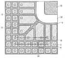
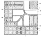
- FIG. 1 is a plan view showing the overall configuration of the MOSFET according to the first embodiment.
- the MOSFET of FIG. 1 includes a gate pad 13 and a cell region 31, and has a generally rectangular shape as a whole.
- a gate pad 13 and a cell region 31 has a generally rectangular shape as a whole.
- the outer shape of the cell region 31 corresponds to the outer shape of the source pad.
- the gate pad 13 and the source pad (cell region 31) are formed with curved corners in order to avoid electric field concentration.
- the corners of the gate pad 13 and the source pad are sharp when viewed macroscopically, but are rounded when viewed microscopically.
- FIG. 2 is a plan view showing a part of the configuration of the MOSFET according to the first embodiment. Specifically, FIG. 2 is an enlarged plan view of a region surrounded by a broken line in FIG. In the cell region 31 of FIG. 1, a plurality of cells (cells 14, 15, 17) indicated by broken lines in FIG.
- the cell 15 is a cell (hereinafter referred to as an “outer periphery”) in a cell region 31 in a plan view in an outer peripheral region that does not face the gate pad 13 and a region that faces a side portion (straight line portion) of the gate pad 13. Part cell 15 ”).
- the outer shape of the outer peripheral cell 15 in plan view is a rectangular shape.
- the cell 17 (first cell) is a cell (hereinafter referred to as “corner cell 17”) disposed in a region (inner corner portion) of the cell region 31 facing the corner (curved portion) of the gate pad 13 in plan view. ).
- the outline shape of the corner cell 17 in plan view is two types of pentagonal shapes (polygonal shape of quadrilateral or more).
- the interior angles of the pentagonal shape of the corner cell 17 are all 90 ° or more.
- FIG. 3 is a diagram showing a region 41 facing the corner of the gate pad 13 in which the corner cell 17 is disposed.
- a region 41 facing the corner of the gate pad 13 corresponds to a region surrounded by a one-dot chain line in FIG.
- the cell region 31 overlapping the region is defined as the first region.
- a square or rectangular region having a line connecting the ends opposite to the gate pad 13 as a diagonal line is defined as the second region. It is prescribed.
- a region where the first region and the second region overlap is defined as a region 41 facing the corner of the gate pad 13 according to the first embodiment.
- the cell 14 (second cell) is arranged in an internal region of the cell region 31 such as the region opposite to the gate pad 13 with respect to the peripheral cell 15 or the corner cell 17 in the plan view.
- This is a cell (hereinafter referred to as “internal cell 14”).
- the internal cell 14 occupies many of the cells arranged in the cell region 31.
- the outer shape of the internal cell 14 in a plan view is a regular square shape (polygonal shape greater than or equal to a square shape).
- the outline shape of the internal cell 14 in plan view may be a rectangle or a square.
- the polygonal vertex of the corner cell 17 is larger than the polygonal vertex of the internal cell 14.
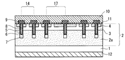
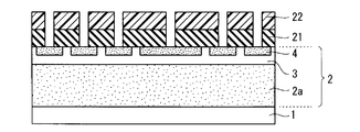
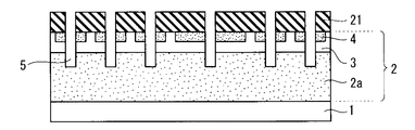
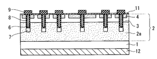
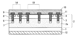
- FIG. 4 and 5 are cross-sectional views showing a part of the structure of the MOSFET according to the first embodiment. Specifically, FIG. 4 is a cross-sectional view taken along the line AA in FIG. 2 and shows a cross-sectional configuration of the internal cell 14. FIG. 5 is a cross-sectional view taken along the line BB in FIG. 2 and shows a cross-sectional configuration of the internal cell 14 and the corner cell 17.
- the internal cell 14 and the corner cell 17 include an n-type SiC substrate 1, an n-type (first conductivity type) epitaxial layer (semiconductor layer) 2, and a p-type (second conductivity type).
- Base region 3 n-type source region 4, gate insulating film 6, protective diffusion layer 7, gate electrode 8, interlayer insulating film 9, source electrode 10, ohmic electrode 11, and drain electrode 12.
- Each of the internal cell 14 and the corner cell 17 has a function of a MOSFET (switching element) by itself.
- MOSFET switching element
- the epitaxial layer 2 is formed by epitaxially growing a SiC layer on the SiC substrate 1. For example, as the SiC substrate 1 and the epitaxial layer 2, an epitaxial substrate in which the epitaxial layer 2 is previously grown on the SiC substrate 1 is applied.
- the base region 3 has a conductivity type opposite to that of the epitaxial layer 2 and is formed on the upper portion (upper surface) of the epitaxial layer 2.
- the remaining epitaxial layer 2 in which the base region 3 is not formed becomes a drift layer 2a.
- a trench (gate trench) 5 is formed in the epitaxial layer 2 and the base region 3. The trench 5 passes through the base region 3, and the bottom of the trench 5 reaches the drift layer 2 a (the epitaxial layer 2 below the base region 3).
- the gate insulating film 6 is provided on the inner surface (bottom surface and side surface) of the trench 5, and the gate electrode 8 is disposed in the trench 5 through the gate insulating film 6.
- the trench 5 is shown to have a pattern (generally a lattice pattern) corresponding to the outer shape of the inner cell 14, the outer peripheral cell 15, and the corner cell 17.
- the gate insulating film 6 and the gate electrode 8 (and thus the interlayer insulating film 9 and the source electrode 10 described later) are omitted from the viewpoint of simplifying the drawing, but the gate disposed in the trench 5.
- the electrode 8 also has a pattern (generally a lattice pattern) corresponding to the outer shape of the internal cell 14, the outer peripheral cell 15, and the corner cell 17 in plan view.
- a silicon oxide film, a gate wiring (polycrystalline silicon), and a silicon film (not shown) are not shown. These are disposed on the SiC substrate 1 in order.
- a contact hole is provided under the gate insulating film 6 adjacent to the gate pad lower well 32, and the gate electrode 8 is electrically connected to the gate pad 13 through the contact hole and the gate wiring. Yes.
- the protective diffusion layer 7 is formed in the drift layer 2 a adjacent to the bottom of the trench 5, that is, the lower portion of the trench 5.
- the protective diffusion layer 7 also has a substantially lattice-like pattern in plan view like the gate electrode 8.
- the protective diffusion layer 7 has a function of promoting the depletion of the drift layer 2a when the MOSFET is turned off and reducing the concentration of the electric field at the bottom of the trench 5 to suppress the breakdown of the gate insulating film 6. .
- a source region 4 is formed in a portion adjacent to the gate insulating film 6 in the upper part of the base region 3.
- the interlayer insulating film 9 is disposed on the source region 4 so as to cover a portion close to the gate insulating film 6 and the gate insulating film 6 and the gate electrode 8.
- a contact hole reaching the base region 3 and a portion far from the gate insulating film 6 in the source region 4 is provided, and a low-resistance ohmic electrode 11 is provided in the contact hole. Yes.
- the source electrode 10 constituting the source pad is disposed on the interlayer insulating film 9 and is electrically connected to the source region 4 and the base region 3 through the ohmic electrode 11.
- Drain electrode 12 is disposed on the lower surface of SiC substrate 1.
- the longest distance among the shortest distances between the longest side and each side facing the side is, for example, the inside
- the cell 14 is configured to be equal to or less than twice the uniform side.
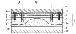
- FIG. 6 is a plan view showing a part of the structure of the related MOSFET in the same manner as FIG.
- the same components as those described above are denoted by the same reference numerals, and components and problems different from the above-described components of the related MOSFET will be described.
- the related MOSFET includes one related corner cell 16 instead of the above-described corner cell 17.
- the outline shape of the related corner cell 16 in plan view has a longer side than the long side of the outer peripheral cell 15.
- the dimensions of the peripheral cell 15 and the internal cell 14 are made different in order to reduce the electric field applied to the peripheral cell 15.
- the corners of the outer shape such as the gate pad 13 have a certain curvature.
- the inventor found that the avalanche breakdown frequently occurs in the related corner cells 16. Therefore, the inventor found that the avalanche breakdown occurs in the related corner cell 16 because the cell on the termination region side of the entire MOSFET in FIG. 1 (for example, the outer peripheral cell 15 disposed at the other corner or side of the cell region 31). ) was considered to be different from the reason that avalanche destruction occurred. Then, the inventor considered the cause of the avalanche breakdown in the related corner cell 16 as follows.
- FIG. 7 is a cross-sectional view showing a part of the configuration of the related MOSFET, specifically, a cross-sectional view taken along the line CC in FIG. FIG. 7 shows a depletion layer end 18 assumed in the related MOSFET.
- the related corner cell 16 is greatly different in size and shape compared to the internal cell 14, and the distance between two opposing sides of the outer shape of the related corner cell 16 is relatively large. It has become. For this reason, as shown in FIG. 7, the depletion layer end 18 is close to the base region 3 at the center of the related corner cell 16. Along with this, the electric field strength at the center of the related corner cell 16 increases, and it is considered that avalanche breakdown is likely to occur. In the terminal region of the cell region 31, the electric field is suppressed by the effect of the termination structure. However, in the inner corner portion away from the terminal region, a unique electric field state is formed. This is thought to have some influence on the likelihood of avalanche destruction.
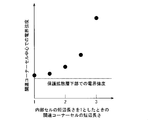
- FIG. 8 is a diagram showing the results. As shown in FIG. 8, the relationship between the cell size ratio and the electric field strength is not linear in a range where the cell size ratio is small (a range such as 2 or less). This is considered to be because the depletion layer extending from the trench 5 and the protective diffusion layer 7 reaches the center of the related corner cell 16.
- the depletion layer thickness is so small that the depletion layer extending from the trench 5 and the protective diffusion layer 7 does not reach the center of the related corner cell 16, and as a result, the related corner cell 16. It is considered that avalanche destruction frequently occurs in
- the longest distance among the shortest distances between the longest side and each side facing the side is appropriately shortened.
- the distance to be appropriately shortened is not more than twice the length of the uniform side of the internal cell 14.
- the distance to be appropriately shortened is set to be twice or less the length of the short side of the internal cell 14.
- the distance that should be appropriately shortened in the corner cell 17 is 1.5 times the length of the uniform side of the internal cell 14.
- the depletion layer extending from the long-side trench 5 and the protective diffusion layer 7 can suppress the depletion layer thickness from being reduced at the center of the corner cell 17.
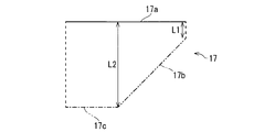
- FIG. 9 is a diagram for explaining a distance that should be appropriately shortened in one of the corner cells 17 shown in FIG.
- the long side 17a of the corner cell 17 is indicated by a solid line
- the sides 17b and 17c facing the long side 17a are indicated by a two-dot chain line and a one-dot chain line, respectively.
- the shortest distance between the long side 17a and the opposite side 17b (the shortest distance among any points on the long side 17a and any point on the side 17b) is L1.
- the shortest distance between the long side 17a and the opposite side 17c (the shortest distance among any points on the long side 17a and any point on the side 17c) is L2.
- the longest distance is L2.
- the distance to be appropriately shortened is L2.
- FIG. 10 to 16 are diagrams showing the steps of the manufacturing method. Specifically, FIG. 10 to FIG. 16 are cross-sectional views along the line BB in FIG. 2, as in FIG.
- an epitaxial layer (semiconductor layer) 2 is formed on SiC substrate 1.
- an n-type low-resistance SiC substrate 1 having a 4H polytype is prepared, and an n-type epitaxial layer 2 is epitaxially grown thereon by a chemical vapor deposition (CVD) method.
- the finally formed drift layer 2a is epitaxially formed so as to ensure an impurity concentration of 1 ⁇ 10 14 cm ⁇ 3 to 1 ⁇ 10 17 cm ⁇ 3 and a thickness of 5 to 200 ⁇ m. Layer 2 was formed.
- a base region 3 and a source region 4 are formed by ion-implanting a predetermined dopant into the surface of the epitaxial layer 2. Thereby, the structure shown in FIG. 10 is obtained.
- the base region 3 is formed by ion implantation of aluminum (Al) which is a p-type impurity.
- Al aluminum
- the depth of Al ion implantation is set to a depth not exceeding the thickness of the epitaxial layer 2 (for example, about 0.5 to 3 ⁇ m).
- the impurity concentration of Al to be implanted is higher than the n-type impurity concentration of the epitaxial layer 2.
- the region of the epitaxial layer 2 deeper than the Al implantation depth remains as the n-type drift layer 2a.
- the base region 3 may be formed by p-type epitaxial growth. Also in this case, the impurity concentration and thickness of the base region 3 are the same as those formed by ion implantation.
- the source region 4 is formed by selectively ion-implanting nitrogen (N) into the surface of the base region 3.
- the outline shape of the source region 4 in plan view is formed in a pattern along the layout of the gate electrode 8 (trench 5) formed in the subsequent process (see FIG. 2).
- the depth of N ion implantation in this step is made shallower than the thickness of the base region 3.
- the impurity concentration of N to be implanted is higher than the p-type impurity concentration of the base region 3 and is, for example, in the range of 1 ⁇ 10 18 cm ⁇ 3 to 1 ⁇ 10 21 cm ⁇ 3 .
- a depletion suppression layer (not shown) formed by ion implantation of nitrogen (N) or phosphorus (P) that is an n-type impurity may be provided below the base region 3.
- N nitrogen
- P phosphorus
- a so-called JFET resistance is generated between the two, in which a current path is exploited by a depletion layer extending from both the base region 3 and the protective diffusion layer 7.
- the depletion suppression layer since the depletion layer is suppressed from extending from the base region 3 or the like at the time of ON, the JFET resistance can be reduced.
- the depletion suppression layer is deeper than the base region 3 and does not exceed the thickness of the epitaxial layer 2, and the thickness is, for example, about 0.5 to 3 ⁇ m.
- the impurity concentration of N in this step is preferably higher than the n-type impurity concentration of the epitaxial layer 2 and 1 ⁇ 10 17 cm ⁇ 3 or more.
- the depletion suppression layer may be formed by n-type epitaxial growth. In this case, the impurity concentration and thickness of the depletion suppression layer are the same as those formed by ion implantation.
- a silicon oxide film 21 of about 1 to 2 ⁇ m is deposited on the surface of the epitaxial layer 2, and an etching mask 22 made of a resist material is formed thereon.
- the etching mask 22 is formed by a photolithography technique in a pattern in which the formation region of the trench 5 in the source region 4 is opened. Since the trench 5 has a substantially lattice pattern in plan view, the pattern of the etching mask 22 includes a matrix pattern obtained by inverting the pattern.
- the silicon oxide film 21 is patterned by a reactive ion etching (RIE) process using the etching mask 22 as a mask. That is, the pattern of the etching mask 22 is transferred to the silicon oxide film 21. Thereby, the structure shown in FIG. 11 is obtained.
- the patterned silicon oxide film 21 becomes an etching mask for the next step.
- RIE reactive ion etching
- a trench 5 that penetrates the source region 4 and the base region 3 and reaches the drift layer 2a is formed by RIE processing using the patterned silicon oxide film 21 as a mask.
- the depth of the trench 5 is not less than the depth of the base region 3 and is, for example, about 1.0 to 6.0 ⁇ m.
- an implantation mask 23 having a pattern exposing the trench 5 (a pattern similar to the etching mask 22) is formed, and ion implantation using the implantation mask 23 as a mask is performed at the bottom of the trench 5.
- a p-type protective diffusion layer 7 is formed.
- Al is used as the p-type impurity of the protective diffusion layer 7.
- the impurity concentration of Al implanted in this step is preferably in the range of 1 ⁇ 10 17 cm ⁇ 3 to 1 ⁇ 10 19 cm ⁇ 3 , for example.
- a (patterned) silicon oxide film 21 which is an etching mask for forming the trench 5 may be used. Thereby, simplification of a manufacturing process and cost reduction can be aimed at.
- the silicon oxide film 21 is used instead of the implantation mask 23, the thickness and etching conditions of the silicon oxide film 21 are adjusted so that the silicon oxide film 21 having a certain thickness remains after the trench 5 is formed. There is a need to.
- annealing for activating the impurities implanted in the above process is performed using a heat treatment apparatus. This annealing is performed, for example, in an inert gas atmosphere such as argon (Ar) gas or in vacuum under processing conditions of 1300 to 1900 ° C. for 30 seconds to 1 hour.
- an inert gas atmosphere such as argon (Ar) gas or in vacuum under processing conditions of 1300 to 1900 ° C. for 30 seconds to 1 hour.
- a silicon oxide film is formed on the entire surface of the epitaxial layer 2 (including the inner surface of the trench 5)
- polysilicon is deposited by a low pressure CVD method so as to fill the trench 5.
- a gate insulating film 6 and a gate electrode 8 are formed in the trench 5 as shown in FIG.
- the silicon oxide film to be the gate insulating film 6 may be formed by thermally oxidizing the surface of the epitaxial layer 2 or may be formed by being deposited on the epitaxial layer 2.
- an interlayer insulating film 9 covering the gate electrode 8 is formed on the entire surface of the epitaxial layer 2 by a low pressure CVD method. Then, as shown in FIG. 15, contact holes reaching the source region 4 and the base region 3 are formed by patterning the interlayer insulating film 9.
- an ohmic electrode 11 is formed on the epitaxial layer 2 (source region 4 and base region 3) exposed at the bottom of the contact hole.
- a metal film mainly composed of nickel (Ni) is formed on the entire surface of the epitaxial layer 2 exposed at the bottom of the contact hole, and silicon carbide and silicon carbide are heat-treated at 600 to 1100 ° C.
- a silicide film to be the ohmic electrode 11 is formed by reaction.
- the unreacted metal film remaining on the interlayer insulating film 9 is removed by wet etching using nitric acid, sulfuric acid or hydrochloric acid, or a mixed solution thereof with hydrogen peroxide.
- the heat treatment may be performed again after the metal film remaining on the interlayer insulating film 9 is removed. In this case, if it is performed at a higher temperature than the previous heat treatment, an ohmic contact with even lower contact resistance is formed.
- an electrode material such as an Al alloy is deposited on the structure obtained in FIG. 15, thereby forming the source electrode 10 on the interlayer insulating film 9 and in the contact hole.
- the drain electrode 12 is formed by depositing an electrode material such as an Al alloy on the lower surface of the SiC substrate 1.
- the outermost shape of the corner cell 17 in plan view is the longest of the shortest distances between the longest side and each side facing the side.
- the long distance is configured to be equal to or less than twice the length of the uniform side or the short side of the internal cell 14.
- the corner cell 17 has more vertices on the polygon than the inner cell 14 on the polygon. Thereby, the layout of the corner cell 17 can be designed more easily than the internal cell 14.
- the interior angles on the polygons of the corner cells 17 are all 90 ° or more. As a result, avalanche breakdown in the corner cell 17 due to electric field concentration can be suppressed, so that the breakdown voltage can be improved.
- the corner cell 17 includes the source region 4 and the source electrode 10 and has a function of a MOSFET alone.
- the epitaxial layer (semiconductor layer) 2 includes a wide band gap semiconductor such as SiC.
- a wide band gap semiconductor such as SiC.
- the wide band gap is not limited to SiC, and may be, for example, a GaN-based material or diamond.
- the drift layer 2a and the SiC substrate 1 serving as the buffer layer have the same conductivity type in the above description, the drift layer 2a and the SiC substrate 1 have different conductivity types. It can also be applied to IGBTs. For example, in the configuration shown in FIGS. 4 and 5, an IGBT configuration is obtained by replacing the n conductivity type of the SiC substrate 1 with a p conductivity type. In such a configuration, the source region 4 and source electrode 10 of the MOSFET correspond to the emitter region and emitter electrode of the IGBT, respectively, and the drain electrode 12 of the MOSFET corresponds to the collector electrode.
- the gate electrode 8 (outer shape of the cell) has a substantially lattice pattern, but the present invention is not limited to this.
- the gate electrode 8 (the outer shape of the cell) may have a generally hexagonal pattern as shown in FIG. 17, for example, or may have a stripe pattern as shown in FIG. Alternatively, other patterns may be used. The same effect as described above can be obtained regardless of the pattern of the gate electrode 8 (the outer shape of the cell).
- the semiconductor device made of SiC which is one of the wide band gap semiconductors, has been described.
- the present invention is not limited to this, and the present invention can also be applied to semiconductor devices made of other wide band gap semiconductors such as gallium nitride (GaN) -based materials and diamond.
- GaN gallium nitride
- FIG. 19 is a plan view showing a part of the configuration of the MOSFET according to the second embodiment of the present invention in the same manner as FIG.
- FIG. 20 is a cross-sectional view showing a part of the structure of the MOSFET according to the second embodiment. Specifically, it is a cross-sectional view along the line DD in FIG. 19, and shows the internal cell 14 and the corner cell. 17 shows a cross-sectional configuration.
- the same or similar components as those described above are denoted by the same reference numerals, and different portions will be mainly described.
- the MOSFET according to the second embodiment is different in that a corner cell 19 is provided instead of the corner cell 17 described in the first embodiment.
- the corner cell 17 according to the first embodiment includes the source region 4.
- the corner cell 19 according to the second embodiment includes the source region 4. It is comprised so that it may not be provided.
- corner cell 19 according to the second embodiment does not include the source region 4, the punch-through phenomenon can be suppressed.
- the corner cell 19 In order to suppress the punch-through phenomenon in the corner cell 19, a method of increasing the impurity concentration of the base region 3 and reducing the depletion layer extending into the base region 3 can be employed. The number of ion implantations increases.
- the corner cell 19 does not include the source region 4, and therefore, as a manufacturing method thereof, the source region 4 is formed in the process of FIG. 10 of the first embodiment. What is necessary is just to change the pattern of the corner cell 19 among patterns. Therefore, the MOSFET can be formed with the same man-hours as in the first embodiment.
- the corner cell 19 according to the second embodiment does not have the function of a MOSFET alone, the on-resistance of the MOSFET is equal to that of the first embodiment corresponding to the area of the corner cell 19 occupying the entire cell region 31. Although it increases above the on-resistance, it is negligibly small compared to variations in MOSFET manufacturing.
- the techniques described in Patent Documents 1 and 2 since all the cells in the outer peripheral portion of the cell region 31 lose the MOSFET function, compared to the increase in the on-resistance of the MOSFET according to the second embodiment. Much bigger.
- the corner cell 19 is configured not to include the source region 4.
- the on-resistance increases to a level that can be almost ignored, but it is possible to realize a high breakdown voltage by suppressing the occurrence of the punch-through phenomenon.
- the longest distance among the shortest distances between the longest side and each side facing the side is the inner side.
- the cell 14 may not be configured to be twice or less the length of the short side of the cell 14.
- FIG. 21 is a cross-sectional view showing a part of the configuration of the MOSFET according to the third embodiment in the same manner as FIG.
- the same or similar components as those described above are denoted by the same reference numerals, and different portions will be mainly described.
- the MOSFET according to the third embodiment is different in that a corner cell 20 is provided instead of the corner cell 17 described in the first embodiment.
- a corner cell 20 is provided instead of the corner cell 17 described in the first embodiment.
- the source electrode 10 and the source region 4 and the base region 3 are electrically connected in the corner cell 17, but as shown in FIG.
- the corner cell 20 according to the third embodiment may be configured not to include the source region 4 as in the second embodiment.
- the source electrode 10, the source region 4, and the base region 3 are configured to be electrically insulated.
- the on-resistance increases to a level that can be almost ignored, but it is possible to realize a high breakdown voltage by suppressing the occurrence of the punch-through phenomenon.
- the longest distance among the shortest distances between the longest side and each side facing the side is the inner
- the cell 14 may not be configured to be twice or less the length of the short side of the cell 14.
- the present invention can be freely combined with each embodiment and each modification, or can be appropriately modified and omitted with each embodiment and each modification.
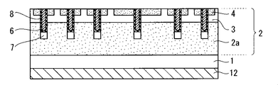
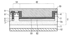
- FIG. 22 is a plan view showing a part of the configuration of the MOSFET according to the fourth embodiment of the present invention in the same manner as FIG.
- FIG. 23 is a cross-sectional view showing a part of the configuration of the MOSFET according to the fourth embodiment in the same manner as in FIG. 20, and more specifically, a cross-sectional view taken along the line CC in FIG.
- the same or similar components as those described above are denoted by the same reference numerals, and different portions will be mainly described.
- the MOSFET according to the fourth embodiment is provided with an ineffective region 42 in which cells (inner cell 14, outer peripheral cell 15, corner cell 17) do not exist, instead of corner cell 17 described in the first embodiment. Is different. That is, as shown in FIG. 4, in the first embodiment, the corner cells 17 are arranged in the region 41 facing the gate pad 13, but as shown in FIG. An invalid area 42 is provided in the area 41.
- a trench 51 which is a second trench that reaches the epitaxial layer 2 below the base region 3 through the base region 3 such as the internal cell 14, is disposed.
- the trench 51 is wider than the trench 5 that is the first trench.
- the invalid region 42 includes an n-type protective diffusion layer 52 that is a second protective diffusion layer.
- the protective diffusion layer 52 is formed at the bottom of the trench 51, like the protective diffusion layer 7 that is the first protective diffusion layer.
- the etching mask 22 on the region 41 may be removed and the silicon oxide film 21 may be removed by RIE.
- RIE is performed using the silicon oxide film 21 as a mask in FIG. 12
- the trenches 51 are all disposed in the region 41, and the bottom of the trench 51 corresponding to the region 41 is protected by subsequent ion implantation.
- a diffusion layer 52 is formed. Thereby, the invalid region 42 can be formed.
- the invalid region 42 according to the fourth embodiment does not have the function of a MOSFET alone, but the increase in the on-resistance associated therewith is substantially negligible as in the second and third embodiments. It is.
- the invalid region 42 including the protective diffusion layer 52 formed at the bottom of the trench 51 is disposed in the region 41 facing the gate pad 13.
Landscapes
- Electrodes Of Semiconductors (AREA)
Abstract
Priority Applications (3)
| Application Number | Priority Date | Filing Date | Title |
|---|---|---|---|
| US15/307,668 US9698221B2 (en) | 2014-05-01 | 2015-03-30 | Semiconductor device |
| JP2016500421A JP5985105B2 (ja) | 2014-05-01 | 2015-03-30 | 半導体装置 |
| CN201580021852.1A CN106463539B (zh) | 2014-05-01 | 2015-03-30 | 半导体装置 |
Applications Claiming Priority (2)
| Application Number | Priority Date | Filing Date | Title |
|---|---|---|---|
| JP2014094383 | 2014-05-01 | ||
| JP2014-094383 | 2014-05-01 |
Publications (1)
| Publication Number | Publication Date |
|---|---|
| WO2015166754A1 true WO2015166754A1 (fr) | 2015-11-05 |
Family
ID=54358491
Family Applications (1)
| Application Number | Title | Priority Date | Filing Date |
|---|---|---|---|
| PCT/JP2015/059968 Ceased WO2015166754A1 (fr) | 2014-05-01 | 2015-03-30 | Dispositif à semi-conducteur |
Country Status (4)
| Country | Link |
|---|---|
| US (1) | US9698221B2 (fr) |
| JP (1) | JP5985105B2 (fr) |
| CN (1) | CN106463539B (fr) |
| WO (1) | WO2015166754A1 (fr) |
Cited By (4)
| Publication number | Priority date | Publication date | Assignee | Title |
|---|---|---|---|---|
| KR20170072496A (ko) * | 2015-12-17 | 2017-06-27 | 삼성전자주식회사 | 수직형 메모리 소자 및 그 형성 방법 |
| WO2022034636A1 (fr) * | 2020-08-11 | 2022-02-17 | 三菱電機株式会社 | Dispositif à semiconducteur à base de carbure de silicium et dispositif de conversion de puissance |
| JP2023011834A (ja) * | 2019-09-13 | 2023-01-24 | 株式会社 日立パワーデバイス | 半導体装置および電力変換装置 |
| WO2023139931A1 (fr) * | 2022-01-20 | 2023-07-27 | 富士電機株式会社 | Dispositif à semi-conducteur |
Families Citing this family (4)
| Publication number | Priority date | Publication date | Assignee | Title |
|---|---|---|---|---|
| KR101949514B1 (ko) * | 2017-06-27 | 2019-02-19 | 현대오트론 주식회사 | 전력 반도체 소자 |
| JP7371335B2 (ja) * | 2019-03-13 | 2023-10-31 | 富士電機株式会社 | 半導体装置 |
| DE102020125371B4 (de) | 2020-09-29 | 2025-05-28 | Infineon Technologies Ag | Package mit Pad, welches eine offene Aussparung hat |
| US12550423B2 (en) | 2023-05-19 | 2026-02-10 | Infineon Technologies Austria Ag | Transistor device having groups of transistor cells with different body region average doping concentrations and different source region densities |
Citations (6)
| Publication number | Priority date | Publication date | Assignee | Title |
|---|---|---|---|---|
| JP2000323707A (ja) * | 1999-05-07 | 2000-11-24 | Hitachi Ltd | 半導体装置 |
| JP2005116822A (ja) * | 2003-10-08 | 2005-04-28 | Toyota Motor Corp | 絶縁ゲート型半導体装置およびその製造方法 |
| JP2006012960A (ja) * | 2004-06-23 | 2006-01-12 | Renesas Technology Corp | パワートランジスタ装置及びそれを用いたパワー制御システム |
| JP2009004655A (ja) * | 2007-06-22 | 2009-01-08 | Toyota Motor Corp | 半導体装置 |
| JP2010251422A (ja) * | 2009-04-13 | 2010-11-04 | Renesas Electronics Corp | 半導体装置及びその製造方法 |
| JP2011029675A (ja) * | 2010-11-11 | 2011-02-10 | Renesas Electronics Corp | 半導体装置 |
Family Cites Families (5)
| Publication number | Priority date | Publication date | Assignee | Title |
|---|---|---|---|---|
| JP4860102B2 (ja) * | 2003-06-26 | 2012-01-25 | ルネサスエレクトロニクス株式会社 | 半導体装置 |
| US7470953B2 (en) | 2003-10-08 | 2008-12-30 | Toyota Jidosha Kabushiki Kaisha | Insulated gate type semiconductor device and manufacturing method thereof |
| JP2005322949A (ja) * | 2005-08-05 | 2005-11-17 | Renesas Technology Corp | 半導体装置 |
| JP4735237B2 (ja) | 2005-12-20 | 2011-07-27 | トヨタ自動車株式会社 | 絶縁ゲート型半導体装置 |
| JP2011100877A (ja) | 2009-11-06 | 2011-05-19 | Toshiba Corp | 半導体装置及びその製造方法 |
-
2015
- 2015-03-30 JP JP2016500421A patent/JP5985105B2/ja active Active
- 2015-03-30 WO PCT/JP2015/059968 patent/WO2015166754A1/fr not_active Ceased
- 2015-03-30 CN CN201580021852.1A patent/CN106463539B/zh active Active
- 2015-03-30 US US15/307,668 patent/US9698221B2/en active Active
Patent Citations (6)
| Publication number | Priority date | Publication date | Assignee | Title |
|---|---|---|---|---|
| JP2000323707A (ja) * | 1999-05-07 | 2000-11-24 | Hitachi Ltd | 半導体装置 |
| JP2005116822A (ja) * | 2003-10-08 | 2005-04-28 | Toyota Motor Corp | 絶縁ゲート型半導体装置およびその製造方法 |
| JP2006012960A (ja) * | 2004-06-23 | 2006-01-12 | Renesas Technology Corp | パワートランジスタ装置及びそれを用いたパワー制御システム |
| JP2009004655A (ja) * | 2007-06-22 | 2009-01-08 | Toyota Motor Corp | 半導体装置 |
| JP2010251422A (ja) * | 2009-04-13 | 2010-11-04 | Renesas Electronics Corp | 半導体装置及びその製造方法 |
| JP2011029675A (ja) * | 2010-11-11 | 2011-02-10 | Renesas Electronics Corp | 半導体装置 |
Cited By (11)
| Publication number | Priority date | Publication date | Assignee | Title |
|---|---|---|---|---|
| KR20170072496A (ko) * | 2015-12-17 | 2017-06-27 | 삼성전자주식회사 | 수직형 메모리 소자 및 그 형성 방법 |
| KR102508897B1 (ko) | 2015-12-17 | 2023-03-10 | 삼성전자주식회사 | 수직형 메모리 소자 및 그 형성 방법 |
| JP2023011834A (ja) * | 2019-09-13 | 2023-01-24 | 株式会社 日立パワーデバイス | 半導体装置および電力変換装置 |
| JP7503612B2 (ja) | 2019-09-13 | 2024-06-20 | 株式会社 日立パワーデバイス | 半導体装置および電力変換装置 |
| WO2022034636A1 (fr) * | 2020-08-11 | 2022-02-17 | 三菱電機株式会社 | Dispositif à semiconducteur à base de carbure de silicium et dispositif de conversion de puissance |
| JPWO2022034636A1 (fr) * | 2020-08-11 | 2022-02-17 | ||
| JP7332812B2 (ja) | 2020-08-11 | 2023-08-23 | 三菱電機株式会社 | 炭化珪素半導体装置および電力変換装置 |
| US12520550B2 (en) | 2020-08-11 | 2026-01-06 | Mitsubishi Electric Corporation | Silicon carbide semiconductor device and power converter |
| WO2023139931A1 (fr) * | 2022-01-20 | 2023-07-27 | 富士電機株式会社 | Dispositif à semi-conducteur |
| JPWO2023139931A1 (fr) * | 2022-01-20 | 2023-07-27 | ||
| JP7704225B2 (ja) | 2022-01-20 | 2025-07-08 | 富士電機株式会社 | 半導体装置 |
Also Published As
| Publication number | Publication date |
|---|---|
| JPWO2015166754A1 (ja) | 2017-04-20 |
| CN106463539A (zh) | 2017-02-22 |
| US9698221B2 (en) | 2017-07-04 |
| CN106463539B (zh) | 2019-05-07 |
| US20170053984A1 (en) | 2017-02-23 |
| JP5985105B2 (ja) | 2016-09-06 |
Similar Documents
| Publication | Publication Date | Title |
|---|---|---|
| JP5985105B2 (ja) | 半導体装置 | |
| JP6049784B2 (ja) | 炭化珪素半導体装置およびその製造方法 | |
| US8648349B2 (en) | Semiconductor device | |
| JP6038391B2 (ja) | 半導体装置 | |
| JP6099749B2 (ja) | 炭化珪素半導体装置およびその製造方法 | |
| JP6312933B2 (ja) | 電力用半導体装置 | |
| JP6140823B2 (ja) | 炭化珪素半導体装置 | |
| US10361266B2 (en) | Semiconductor device | |
| JP7029710B2 (ja) | 半導体装置 | |
| JP6463214B2 (ja) | 半導体装置 | |
| JP6705155B2 (ja) | 半導体装置および半導体装置の製造方法 | |
| JP6862782B2 (ja) | 半導体装置および半導体装置の製造方法 | |
| WO2015076020A1 (fr) | Dispositif semi-conducteur | |
| JP2011040431A (ja) | 半導体装置およびその製造方法 | |
| JP6589263B2 (ja) | 半導体装置 | |
| JP2017092364A (ja) | 半導体装置および半導体装置の製造方法 | |
| JP4972293B2 (ja) | 半導体装置およびその製造方法 | |
| JP5907097B2 (ja) | 半導体装置 | |
| JP6771433B2 (ja) | 半導体装置 | |
| JP2016058661A (ja) | 半導体装置 | |
| JP7074173B2 (ja) | 半導体装置および半導体装置の製造方法 |
Legal Events
| Date | Code | Title | Description |
|---|---|---|---|
| 121 | Ep: the epo has been informed by wipo that ep was designated in this application |
Ref document number: 15786556 Country of ref document: EP Kind code of ref document: A1 |
|
| ENP | Entry into the national phase |
Ref document number: 2016500421 Country of ref document: JP Kind code of ref document: A |
|
| WWE | Wipo information: entry into national phase |
Ref document number: 15307668 Country of ref document: US |
|
| NENP | Non-entry into the national phase |
Ref country code: DE |
|
| 122 | Ep: pct application non-entry in european phase |
Ref document number: 15786556 Country of ref document: EP Kind code of ref document: A1 |