WO2015174263A1 - 回路構成体および電気接続箱 - Google Patents
回路構成体および電気接続箱 Download PDFInfo
- Publication number
- WO2015174263A1 WO2015174263A1 PCT/JP2015/062674 JP2015062674W WO2015174263A1 WO 2015174263 A1 WO2015174263 A1 WO 2015174263A1 JP 2015062674 W JP2015062674 W JP 2015062674W WO 2015174263 A1 WO2015174263 A1 WO 2015174263A1
- Authority
- WO
- WIPO (PCT)
- Prior art keywords
- bus bars
- circuit board
- adhesive
- opening
- adhesive sheet
- Prior art date
- Legal status (The legal status is an assumption and is not a legal conclusion. Google has not performed a legal analysis and makes no representation as to the accuracy of the status listed.)
- Ceased
Links
Images



Classifications
-
- H—ELECTRICITY
- H02—GENERATION; CONVERSION OR DISTRIBUTION OF ELECTRIC POWER
- H02G—INSTALLATION OF ELECTRIC CABLES OR LINES, OR OF COMBINED OPTICAL AND ELECTRIC CABLES OR LINES
- H02G3/00—Installations of electric cables or lines or protective tubing therefor in or on buildings, equivalent structures or vehicles
- H02G3/02—Details
- H02G3/08—Distribution boxes; Connection or junction boxes
- H02G3/16—Distribution boxes; Connection or junction boxes structurally associated with support for line-connecting terminals within the box
-
- H—ELECTRICITY
- H05—ELECTRIC TECHNIQUES NOT OTHERWISE PROVIDED FOR
- H05K—PRINTED CIRCUITS; CASINGS OR CONSTRUCTIONAL DETAILS OF ELECTRIC APPARATUS; MANUFACTURE OF ASSEMBLAGES OF ELECTRICAL COMPONENTS
- H05K7/00—Constructional details common to different types of electric apparatus
- H05K7/20—Modifications to facilitate cooling, ventilating, or heating
- H05K7/20845—Modifications to facilitate cooling, ventilating, or heating for automotive electronic casings
- H05K7/20854—Heat transfer by conduction from internal heat source to heat radiating structure
-
- H—ELECTRICITY
- H05—ELECTRIC TECHNIQUES NOT OTHERWISE PROVIDED FOR
- H05K—PRINTED CIRCUITS; CASINGS OR CONSTRUCTIONAL DETAILS OF ELECTRIC APPARATUS; MANUFACTURE OF ASSEMBLAGES OF ELECTRICAL COMPONENTS
- H05K1/00—Printed circuits
- H05K1/02—Details
- H05K1/0201—Thermal arrangements, e.g. for cooling, heating or preventing overheating
- H05K1/0203—Cooling of mounted components
-
- H—ELECTRICITY
- H05—ELECTRIC TECHNIQUES NOT OTHERWISE PROVIDED FOR
- H05K—PRINTED CIRCUITS; CASINGS OR CONSTRUCTIONAL DETAILS OF ELECTRIC APPARATUS; MANUFACTURE OF ASSEMBLAGES OF ELECTRICAL COMPONENTS
- H05K1/00—Printed circuits
- H05K1/18—Printed circuits structurally associated with non-printed electric components
- H05K1/181—Printed circuits structurally associated with non-printed electric components associated with surface mounted components
-
- H—ELECTRICITY
- H05—ELECTRIC TECHNIQUES NOT OTHERWISE PROVIDED FOR
- H05K—PRINTED CIRCUITS; CASINGS OR CONSTRUCTIONAL DETAILS OF ELECTRIC APPARATUS; MANUFACTURE OF ASSEMBLAGES OF ELECTRICAL COMPONENTS
- H05K7/00—Constructional details common to different types of electric apparatus
- H05K7/02—Arrangements of circuit components or wiring on supporting structure
- H05K7/06—Arrangements of circuit components or wiring on supporting structure on insulating boards, e.g. wiring harnesses
-
- H—ELECTRICITY
- H05—ELECTRIC TECHNIQUES NOT OTHERWISE PROVIDED FOR
- H05K—PRINTED CIRCUITS; CASINGS OR CONSTRUCTIONAL DETAILS OF ELECTRIC APPARATUS; MANUFACTURE OF ASSEMBLAGES OF ELECTRICAL COMPONENTS
- H05K2201/00—Indexing scheme relating to printed circuits covered by H05K1/00
- H05K2201/10—Details of components or other objects attached to or integrated in a printed circuit board
- H05K2201/10007—Types of components
- H05K2201/10015—Non-printed capacitor
-
- H—ELECTRICITY
- H05—ELECTRIC TECHNIQUES NOT OTHERWISE PROVIDED FOR
- H05K—PRINTED CIRCUITS; CASINGS OR CONSTRUCTIONAL DETAILS OF ELECTRIC APPARATUS; MANUFACTURE OF ASSEMBLAGES OF ELECTRICAL COMPONENTS
- H05K2201/00—Indexing scheme relating to printed circuits covered by H05K1/00
- H05K2201/10—Details of components or other objects attached to or integrated in a printed circuit board
- H05K2201/10007—Types of components
- H05K2201/10022—Non-printed resistor
-
- H—ELECTRICITY
- H05—ELECTRIC TECHNIQUES NOT OTHERWISE PROVIDED FOR
- H05K—PRINTED CIRCUITS; CASINGS OR CONSTRUCTIONAL DETAILS OF ELECTRIC APPARATUS; MANUFACTURE OF ASSEMBLAGES OF ELECTRICAL COMPONENTS
- H05K2201/00—Indexing scheme relating to printed circuits covered by H05K1/00
- H05K2201/10—Details of components or other objects attached to or integrated in a printed circuit board
- H05K2201/10007—Types of components
- H05K2201/1003—Non-printed inductor
-
- H—ELECTRICITY
- H05—ELECTRIC TECHNIQUES NOT OTHERWISE PROVIDED FOR
- H05K—PRINTED CIRCUITS; CASINGS OR CONSTRUCTIONAL DETAILS OF ELECTRIC APPARATUS; MANUFACTURE OF ASSEMBLAGES OF ELECTRICAL COMPONENTS
- H05K2201/00—Indexing scheme relating to printed circuits covered by H05K1/00
- H05K2201/10—Details of components or other objects attached to or integrated in a printed circuit board
- H05K2201/10227—Other objects, e.g. metallic pieces
- H05K2201/10272—Busbars, i.e. thick metal bars mounted on the printed circuit board [PCB] as high-current conductors
Definitions
- the technology disclosed in this specification relates to a circuit structure and an electrical junction box.
- the electronic components mounted on the circuit board are small and have excellent functions.
- a heat radiating member is provided on the surface of the circuit board 112 opposite to the surface on which the electronic component 115 is disposed.
- a circuit structure 111 having a configuration in which 130 is provided is conceivable.
- an opening 113 is provided in a region of the circuit board 112 corresponding to the electronic component 115, and the surface of the circuit board 112 opposite to the surface on which the electronic component 115 is disposed.
- a configuration in which a plurality of bus bars 120 are provided and the terminals 117 of the electronic component 115 are connected to the bus bars 120 exposed through the openings 113 is conceivable. By configuring a power circuit with a plurality of bus bars 120, a large current can flow through the power circuit.
- the electronic component 115 when the electronic component 115 is connected to the plurality of bus bars 120 through the openings 113 provided in the circuit board 112, as shown in FIG. 7, the heat dissipating member laminated on the surface of the bus bar 120 on the opposite side of the circuit board 112.
- the adhesive 135 for bonding enters the gap S between the adjacent bus bars 120 and contacts the lower surface of the main body 116 of the electronic component 115.
- the adhesive 135 expands due to heat generated from the circuit board 112 or the electronic component 115, or conversely, when the shrinkage occurs due to cooling, the electronic component 115 is pushed up by the adhesive 135 or pulled in. There is a risk that a connection failure such as a crack may occur in the connection portion between the terminal 117 and the bus bar 120.
- the technology disclosed in the present specification has been completed based on the above circumstances, and an object thereof is to provide a circuit structure and an electrical junction box with high connection reliability.
- the technology disclosed in this specification includes a circuit board having a connection opening, a plurality of bus bars stacked on one surface side of the circuit board via an adhesive sheet, a main body, and a plurality of lead terminals.
- the lead terminals are connected to the plurality of bus bars exposed through the connection openings, so that the electronic components disposed on the other surface side of the circuit board are opposite to the circuit board among the plurality of bus bars.
- the gap between adjacent bus bars is covered with the adhesive sheet in the connection opening, so that the adhesive that has entered the gap is the lower surface of the main body of the electronic component. Direct contact with the is prevented. Further, since the adhesive sheet arranged in this way has an action of suppressing the adhesive in the gap, it is possible to reduce the influence that the electronic component receives from the adhesive as compared with the case where the adhesive sheet is not arranged. . Therefore, a circuit structure and an electrical junction box with high connection reliability can be obtained.
- the technology disclosed in the present specification is an electrical junction box in which the circuit configuration body is accommodated in a case.
- connection reliability can be improved in a circuit configuration body or an electrical junction box.
- the electrical junction box 10 of the present embodiment includes a circuit board 11 and a circuit structure 11 including a heat sink 30 and a synthetic resin case 40 that houses the circuit structure 11.
- the upper side in FIG. 1 is described as the front side or the upper side, and the lower side is described as the back side or the lower side.
- the circuit structure 11 includes a circuit board 12, a coil 15 (an example of an electronic component) disposed on the front surface (upper surface in FIG. 1) of the circuit board 12, and the back surface of the circuit board 12 (FIG. 1 is provided with a plurality of bus bars 20 disposed on the lower surface of the bus bar 20 and a heat sink 30 (see FIG. 5) disposed on the back surface of the bus bar 20.
- the circuit board 12 is substantially L-shaped, and a conductive circuit (not shown) is formed on the surface thereof by a printed wiring technique.
- the coil 15 is a surface-mounting type coil, and has a rectangular parallelepiped main body portion 16 as shown in FIGS. 1 and 5, and a pair of peripheral portions of the bottom surface of the main body portion 16 are arranged around the opposing edge portions.
- the lead terminal 17 is provided.
- the plurality of bus bars 20 are formed by pressing a metal plate into a predetermined shape.
- the bus bar 20 has a generally rectangular shape, and is arranged in a predetermined pattern with a gap S between adjacent bus bars 20.
- a connecting piece 21 protruding outward is formed integrally with the bus bar 20 at the side edge of some bus bars 20.
- Bolt mounting holes 21A for inserting bolts are formed through these connection pieces 21. Bolts (not shown) are inserted into these bolt mounting holes 21A and screwed with power supply terminals mounted on the vehicle. As a result, the connection piece 21 is electrically connected to an external power source.
- the plurality of bus bars 20 are bonded to the back surface of the circuit board 12 via an insulating adhesive sheet 25.
- the outer shape of the adhesive sheet 25 is substantially the same as the outer shape of the circuit board 12.
- connection opening 13 for mounting the coil 15 on the bus bar 20 is formed at a position on the circuit board 12 where the coil 15 is disposed.
- the portion of the connection opening 13 where the main body portion 16 of the coil 15 is disposed opens in a rectangular shape slightly larger than the bottom surface of the main body portion 16.
- an opening having a short width (hereinafter referred to as an extension portion 13A) is provided on the side of the pair of edges where the lead terminal 17 of the coil 15 is located.
- a part of the pair of bus bars 20 is disposed in the connection opening 13.
- the adhesive sheet 25 is provided with a pair of sheet openings 26 for mounting the lead terminals 17 of the coil 15 on the bus bar 20.
- the seat opening 26 is a substantially square opening, and a part of the seat opening 26 is provided at a position overlapping the pair of expansion portions 13 ⁇ / b> A. More specifically, the seat opening 26 is provided such that a part of the opening edge is located slightly outside the opening edge of the expansion portion 13A (so as to have a slightly larger opening size), A part of the bus bar 20 is exposed in the connection opening 13 of the circuit board 12.
- the sheet opening 26 is provided in the connection opening 13 so that the opening edge thereof does not cover the gap S between the adjacent bus bars 20.
- the adhesive sheet 25 is configured to cover the gap S between the adjacent bus bars 20 from the upper surface side in the connection opening 13.
- the coil 15 is disposed on the surface side of the circuit board 12 in a region where the connection opening 13 is provided.
- the lead terminal 17 of the coil 15 is connected to the surface of the bus bar 20 exposed through the connection opening 13 and the sheet opening 26 by a known method such as soldering.
- the heat sink 30 is disposed on the lower surface (back surface) of the bus bar 20 (see FIG. 5).
- the heat radiating plate 30 is a plate-shaped member made of a metal material having excellent thermal conductivity such as aluminum or aluminum alloy, and has a function of radiating heat generated in the circuit board 12 and the coil 15.
- the heat sink 30 is bonded to the back side of the bus bar 20 with, for example, a thermosetting adhesive 35.
- the adhesive 35 is an adhesive having insulating properties and thermal conductivity.
- an adhesive sheet 25 cut into a predetermined shape is overlaid on a lower surface of a circuit board 12 having a conductive path formed on the surface thereof by a printed wiring technique, and a plurality of bus bars 20 are connected to predetermined surfaces. Pressurize in a state where they are arranged in a pattern. Thereby, the circuit board 12 and the plurality of bus bars 20 are bonded and fixed to each other via the adhesive sheet 25.
- solder is applied to a predetermined position of the circuit board 12 by screen printing. Thereafter, the coil 15 is placed at a predetermined position, and reflow soldering is executed.
- the adhesive 35 is applied to the upper surface of the heat sink 30 and the circuit board 12 on which the coil 15 and the plurality of bus bars 20 are arranged is overlaid from above.
- the adhesive sheet 25 since the gap S between the adjacent bus bars 20 located in the connection opening 13 of the circuit board 12 is covered with the adhesive sheet 25, the adhesive 35 that has entered the gap S is the main body of the coil 15. There is no direct contact with the lower surface of the part 16 (see FIG. 5). Thereafter, the adhesive 35 is cured by heating.
- circuit board 12 (circuit structure) on which the heat sink 30 is stacked is accommodated in the case 40 to obtain the electrical connection box 10.
- the operation and effect of the electrical junction box 10 according to the present embodiment will be described.
- the adhesive 35 even when the adhesive 35 enters the gap S between the adjacent bus bars 20 in the connection opening 13, the adhesive 35 is suppressed in the gap S by the adhesive sheet 25. Therefore, even when the adhesive 35 expands due to heat or contracts conversely, the influence of the coil 15 from the adhesive 35 can be reduced as compared with the case where the adhesive sheet 25 is not disposed. That is, it is possible to obtain a circuit structure and an electrical junction box with high connection reliability.
- the configuration in which the pair of lead terminals 17 is connected to the bus bar 20 is shown.
- one of the lead terminals 17 may be connected to the conductive path of the circuit board 12, and in this case, One sheet opening 26 of the adhesive sheet 25 may be provided.
- the position, shape, and number of the sheet openings 26 are not limited to the above embodiment, and can be changed as appropriate.
- the point is that the lead terminal 17 can be connected to the bus bar 20 and the adhesive sheet 25 covers the gap S between the adjacent bus bars 20.
Landscapes
- Engineering & Computer Science (AREA)
- Microelectronics & Electronic Packaging (AREA)
- Architecture (AREA)
- Civil Engineering (AREA)
- Structural Engineering (AREA)
- Physics & Mathematics (AREA)
- Thermal Sciences (AREA)
- Connection Or Junction Boxes (AREA)
- Cooling Or The Like Of Electrical Apparatus (AREA)
Abstract
接続用開口部13を有する回路基板12と、回路基板12の一面側に接着シート25を介して積層された複数のバスバー20と、本体部16および複数のリード端子17を有し、リード端子17が接続用開口部13を通して露出された複数のバスバー20に接続されることにより回路基板12の他面側に配されたコイル15と、複数のバスバー20のうち回路基板12と反対側の面に接着剤35を介して積層された放熱板30と、を備えた回路構成体11であって、接着シート25は、複数のバスバー20を露出させて複数のリード端子17を複数のバスバー20に接続させるためのシート開口部26を有し、かつ、接続用開口部13内に位置する複数のバスバー20の間の隙間Sを覆っている。
Description
本明細書によって開示される技術は、回路構成体および電気接続箱に関する。
従来より、車載電装品の通電や断電を実行する装置として、種々の電子部品が実装された回路基板を備える回路構成体をケースに収容してなるものが知られている。
このような装置において、回路基板に実装される電子部品は小型で優れた機能を有する。
しかし、これらの電子部品は比較的発熱量が大きいため、電子部品から発生した熱がケース内にこもるとケース内が高温になり、ケース内に収容された電子部品の性能が低下する虞があった。
そこで、回路基板や電子部品から発生した熱を放熱する様々な構造として、例えば、図7に示すように、回路基板112のうち電子部品115が配された面の反対側の面に、放熱部材130を設けた構成の回路構成体111が考えられる。
一方、図6および図7に示すように、回路基板112のうち電子部品115に対応する領域に開口113を設けるとともに、回路基板112のうち電子部品115が配される面の反対側の面に複数のバスバー120を設け、電子部品115の端子117を、開口113を通して露出されたバスバー120に接続する構成が考えられる。複数のバスバー120によって電力回路を構成することにより、電力回路に大電流を流すことが可能となる。
しかし、回路基板112に設けられた開口113を通して電子部品115を複数のバスバー120に接続する場合、図7に示すように、バスバー120のうち回路基板112の反対側に面に積層された放熱部材接着用の接着剤135が隣り合うバスバー120の間の隙間S内に進入し、電子部品115の本体部116の下面に接触する場合がある。このような状態となると、回路基板112や電子部品115から発生した熱により接着剤135が膨張したり、逆に、冷却により収縮した場合に、電子部品115が接着剤135により押し上げられたり、引き込まれたりして、端子117とバスバー120との接続部分にクラックが入る等の接続不良が生じる虞がある。
本明細書に開示される技術は上記のような事情に基づいて完成されたものであって、接続信頼性が高い回路構成体および電気接続箱を提供することを目的とするものである。
本明細書に開示される技術は、接続用開口部を有する回路基板と、前記回路基板の一面側に接着シートを介して積層された複数のバスバーと、本体部および複数のリード端子を有し、前記リード端子が前記接続用開口部を通して露出された前記複数のバスバーに接続されることにより前記回路基板の他面側に配された電子部品と、前記複数のバスバーのうち前記回路基板と反対側の面に接着剤を介して積層された放熱板と、を備えた回路構成体であって、前記接着シートは、前記複数のバスバーを露出させて前記複数のリード端子を前記複数のバスバーに接続させるためのシート開口部を有し、かつ、前記接続用開口部内に位置する前記複数のバスバーの間の隙間を覆っていることを特徴とする。
本明細書に開示される技術によれば、接続用開口部内において、隣り合うバスバーの間の隙間は接着シートにより覆われているから、隙間内に進入した接着剤が電子部品の本体部の下面に直接接触することが防止される。また、このように配された接着シートは接着剤を隙間内に抑え込む作用を有するから、接着シートが配されていない場合と比較して、電子部品が接着剤から受ける影響を軽減させることができる。よって、接続信頼性が高い回路構成体および電気接続箱を得ることができる。
本明細書に開示される技術は、上記回路構成体をケースに収容してなる電気接続箱である。
本明細書に開示された技術によれば、回路構成体又は電気接続箱において、接続信頼性を向上させることができる。
一実施形態を図1ないし図5によって説明する。
本実施形態の電気接続箱10は、回路基板12、および、放熱板30を含む回路構成体11と、回路構成体11を収容する合成樹脂製のケース40と、を備える。なお、以下の説明においては、図1における上側を、表側又は上側とし、下側を、裏側又は下側として説明する。
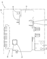
図1に示すように、回路構成体11は、回路基板12と、回路基板12の表面(図1における上面)に配されたコイル15(電子部品の一例)と、回路基板12の裏面(図1における下面)に配された複数のバスバー20と、バスバー20の裏面に配された放熱板30(図5参照)とを備える。
回路基板12は略L字形状をなし、その表面には、プリント配線技術により図示しない導電回路が形成されている。
コイル15は表面実装型のコイルであって、図1および図5に示すように、直方体状の本体部16を有し、本体部16の底面のうちの対向する2辺の縁部周辺に一対のリード端子17が設けられた形態をなしている。
複数のバスバー20は、金属板材を所定形状にプレス加工してなる。バスバー20は概ね矩形状をなしており、隣り合うバスバー20との間に隙間Sを介して所定のパターンで配策されている。いくつかのバスバー20の側縁には、外方に突出する接続片21が、バスバー20と一体に形成されている。これら接続片21にはボルトを挿通するためのボルト取り付け孔21Aが貫通して形成されており、これらのボルト取り付け孔21Aに図示しないボルトが挿通されるとともに車両に取り付けられた電源端子と螺合されることにより、接続片21は外部電源と電気的に接続されるようになっている。
複数のバスバー20は、回路基板12の裏面に、絶縁性の接着シート25を介して接着されている。接着シート25の外形は、回路基板12の外形とほぼ同形状をなしている。
図1に示すように、回路基板12のうちコイル15が配される位置には、コイル15をバスバー20上に実装するための接続用開口部13が形成されている。図4に示すように、接続用開口部13のうちコイル15の本体部16が配される部分は、本体部16の底面より僅かに大きい矩形状に開口している。また、コイル15のリード端子17が位置する一対の縁部側には、幅が短い開口(以下拡張部13Aとする)が拡張して設けられている。接続用開口部13内には、一対のバスバー20の一部が配されている。
一方、接着シート25には、コイル15のリード端子17をバスバー20上に実装するための一対のシート開口部26が設けられている。シート開口部26は、図3に示すように、略正方形状の開口であって、その一部が一対の拡張部13Aに重なる位置に設けられている。より詳細には、シート開口部26は、その開口縁部の一部が拡張部13Aの開口縁部より僅かに外側に位置するように(やや大きな開口寸法となるように)設けられており、回路基板12の接続用開口部13内において、バスバー20の一部を露出させている。
また、シート開口部26は、接続用開口部13内において、その開口縁部が隣り合うバスバー20の間の隙間Sにかからないように設けられている。換言すると、接着シート25は、接続用開口部13内において、隣り合うバスバー20の間の隙間Sを上面側から覆う形態とされている。
コイル15は、回路基板12の表面側のうち、接続用開口部13が設けられた領域に配されている。本実施形態においては、コイル15のリード端子17は、例えばハンダ付け等公知の手法により、接続用開口部13およびシート開口部26を通して露出されたバスバー20の表面に接続されている。
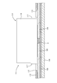
バスバー20の下面(裏面)には、放熱板30が配置されている(図5参照)。放熱板30は、例えばアルミニウムやアルミニウム合金等の熱伝導性に優れる金属材料からなる板状部材であり、回路基板12およびコイル15において発生した熱を放熱する機能を有する。放熱板30は、例えば熱硬化性の接着剤35によりバスバー20の裏面側に接着されている。接着剤35は、絶縁性かつ熱伝導性を有する接着剤である。
続いて、本実施形態に係る電気接続箱10の製造工程の一例を説明する。まず、図1に示すように、表面にプリント配線技術により導電路が形成された回路基板12の下面に、所定の形状に切断された接着シート25を重ね合わせるとともに、複数のバスバー20を所定のパターンで並べた状態で加圧する。これにより、回路基板12および複数のバスバー20は接着シート25を介して互いに接着・固定される。この状態において、複数のバスバー20の上面の一部(コイル15のリード端子17が実装される領域)は、回路基板12の接続用開口部13および接着シート25のシート開口部26を通して露出された状態とされている。
続いて、スクリーン印刷により回路基板12の所定の位置にはんだを塗布する。その後、所定の位置にコイル15を載置し、リフローはんだ付けを実行する。
次に、放熱板30の上面に接着剤35を塗布し、コイル15および複数のバスバー20を配した回路基板12を上方から重ね合わせる。この時、回路基板12の接続用開口部13内に位置する隣り合うバスバー20の間の隙間Sは、接着シート25により覆われているから、隙間Sに進入した接着剤35がコイル15の本体部16の下面に直接接触することはない(図5参照)。その後加熱を行うことにより、接着剤35を硬化させる。
最後に、放熱板30が重ねられた回路基板12(回路構成体)をケース40内に収容し、電気接続箱10とする。
続いて、本実施形態に係る電気接続箱10の作用、効果について説明する。本実施形態によれば、接続用開口部13内において隣り合うバスバー20の間の隙間Sに接着剤35が進入した場合でも、接着剤35は接着シート25により隙間S内に抑え込まれる。従って、接着剤35が熱により膨張したり、逆に収縮した場合でも、接着シート25が配されていない場合と比較して、コイル15が接着剤35から受ける影響を軽減させることができる。すなわち、接続信頼性が高い回路構成体および電気接続箱を得ることができる。
<他の実施形態>
本明細書によって開示される技術は上記記述及び図面によって説明した実施形態に限定されるものではなく、例えば次のような種々の態様も含まれる。
本明細書によって開示される技術は上記記述及び図面によって説明した実施形態に限定されるものではなく、例えば次のような種々の態様も含まれる。
(1)上記実施形態では、一対のリード端子17をバスバー20に接続する構成を示したが、例えば、リード端子17の一方を回路基板12の導電路に接続する構成としてもよく、この場合、接着シート25のシート開口部26はひとつ設ければよい。
(2)シート開口部26の位置や形状、数は、上記実施形態に限るものではなく、適宜変更することができる。要は、リード端子17がバスバー20に接続可能で、かつ、接着シート25が隣り合うバスバー20の間の隙間Sを覆う構成であればよい。
(3)上記実施形態では、コイル15を実装する例を示したが、コイル15に限らず、コンデンサやシャント抵抗等、他の電子部品を実装する場合に適用することもできる。
10:電気接続箱
11:回路構成体
12:回路基板
13:接続用開口部
15:コイル
16:本体部
17:リード端子
20:バスバー
25:接着シート
26:シート開口部
30:放熱板
35:接着剤
40:ケース
S:隙間
11:回路構成体
12:回路基板
13:接続用開口部
15:コイル
16:本体部
17:リード端子
20:バスバー
25:接着シート
26:シート開口部
30:放熱板
35:接着剤
40:ケース
S:隙間
Claims (2)
- 接続用開口部を有する回路基板と、
前記回路基板の一面側に接着シートを介して積層された複数のバスバーと、
本体部および複数のリード端子を有し、前記リード端子が前記接続用開口部を通して露出された前記複数のバスバーに接続された電子部品と、
前記複数のバスバーのうち前記回路基板と反対側の面に接着剤を介して積層された放熱板と、を備えた回路構成体であって、
前記接着シートは、前記複数のバスバーを露出させて前記複数のリード端子を前記複数のバスバーに接続させるためのシート開口部を有し、かつ、前記接続用開口部内に位置する前記複数のバスバーの間の隙間を覆っている回路構成体。 - 請求項1に記載の回路構成体をケースに収容してなる電気接続箱。
Priority Applications (3)
| Application Number | Priority Date | Filing Date | Title |
|---|---|---|---|
| US15/306,661 US9899818B2 (en) | 2014-05-14 | 2015-04-27 | Circuit assembly and electrical junction box |
| CN201580021877.1A CN106256063B (zh) | 2014-05-14 | 2015-04-27 | 电路结构体及电连接箱 |
| DE112015002230.9T DE112015002230B4 (de) | 2014-05-14 | 2015-04-27 | Schaltungsbaugruppe und elektrischer Verteiler |
Applications Claiming Priority (2)
| Application Number | Priority Date | Filing Date | Title |
|---|---|---|---|
| JP2014100258A JP6119664B2 (ja) | 2014-05-14 | 2014-05-14 | 回路構成体および電気接続箱 |
| JP2014-100258 | 2014-05-14 |
Publications (1)
| Publication Number | Publication Date |
|---|---|
| WO2015174263A1 true WO2015174263A1 (ja) | 2015-11-19 |
Family
ID=54479806
Family Applications (1)
| Application Number | Title | Priority Date | Filing Date |
|---|---|---|---|
| PCT/JP2015/062674 Ceased WO2015174263A1 (ja) | 2014-05-14 | 2015-04-27 | 回路構成体および電気接続箱 |
Country Status (5)
| Country | Link |
|---|---|
| US (1) | US9899818B2 (ja) |
| JP (1) | JP6119664B2 (ja) |
| CN (1) | CN106256063B (ja) |
| DE (1) | DE112015002230B4 (ja) |
| WO (1) | WO2015174263A1 (ja) |
Cited By (1)
| Publication number | Priority date | Publication date | Assignee | Title |
|---|---|---|---|---|
| US20190150304A1 (en) * | 2016-05-12 | 2019-05-16 | Autonetworks Technologies, Ltd. | Power distribution board |
Families Citing this family (5)
| Publication number | Priority date | Publication date | Assignee | Title |
|---|---|---|---|---|
| JP6709968B2 (ja) * | 2019-08-09 | 2020-06-17 | パナソニックIpマネジメント株式会社 | 配線器具 |
| CN111093319B (zh) * | 2019-12-16 | 2023-07-28 | 合肥阳光电动力科技有限公司 | 一种晶体管的布线装置和方法 |
| JP6814987B2 (ja) * | 2020-01-23 | 2021-01-20 | パナソニックIpマネジメント株式会社 | 配線器具 |
| JP7596903B2 (ja) * | 2021-04-09 | 2024-12-10 | 住友電装株式会社 | 電気接続箱 |
| WO2026054426A1 (ko) * | 2024-09-03 | 2026-03-12 | 엘지이노텍 주식회사 | 기판모듈 및 이를 포함하는 전자부품모듈 |
Citations (3)
| Publication number | Priority date | Publication date | Assignee | Title |
|---|---|---|---|---|
| JP2005080354A (ja) * | 2003-08-29 | 2005-03-24 | Auto Network Gijutsu Kenkyusho:Kk | 回路構成体 |
| JP2005117719A (ja) * | 2003-10-03 | 2005-04-28 | Auto Network Gijutsu Kenkyusho:Kk | 回路構成体製造用接着シート及び接着シートを用いた回路構成体の製造方法 |
| JP2005228799A (ja) * | 2004-02-10 | 2005-08-25 | Auto Network Gijutsu Kenkyusho:Kk | 回路構成体及びその製造方法 |
Family Cites Families (10)
| Publication number | Priority date | Publication date | Assignee | Title |
|---|---|---|---|---|
| JP3907461B2 (ja) * | 2001-12-03 | 2007-04-18 | シャープ株式会社 | 半導体モジュールの製造方法 |
| JP4261213B2 (ja) * | 2003-02-14 | 2009-04-30 | 株式会社オートネットワーク技術研究所 | 回路構成体の製造方法 |
| CN2831425Y (zh) * | 2005-07-01 | 2006-10-25 | 光宝科技股份有限公司 | 一种半导体封装结构 |
| JP3983786B2 (ja) * | 2005-11-15 | 2007-09-26 | シャープ株式会社 | プリント配線基板 |
| CN100533721C (zh) * | 2006-08-28 | 2009-08-26 | 力成科技股份有限公司 | 芯片封装结构及其制造方法 |
| CN100552963C (zh) * | 2007-03-28 | 2009-10-21 | 精材科技股份有限公司 | 集成电路封装体及其制作方法 |
| CN103025047A (zh) * | 2011-09-22 | 2013-04-03 | 常州紫寅电子电路有限公司 | 高密度高速度的印制电路板 |
| JP5741947B2 (ja) * | 2011-10-31 | 2015-07-01 | 株式会社オートネットワーク技術研究所 | 回路構成体 |
| CN203282754U (zh) * | 2013-05-25 | 2013-11-13 | 宸鸿科技(厦门)有限公司 | 软性电路板 |
| CN103489838B (zh) * | 2013-10-15 | 2016-04-06 | 北京大学 | 一种强化散热三维封装结构及其封装方法 |
-
2014
- 2014-05-14 JP JP2014100258A patent/JP6119664B2/ja not_active Expired - Fee Related
-
2015
- 2015-04-27 DE DE112015002230.9T patent/DE112015002230B4/de not_active Expired - Fee Related
- 2015-04-27 WO PCT/JP2015/062674 patent/WO2015174263A1/ja not_active Ceased
- 2015-04-27 CN CN201580021877.1A patent/CN106256063B/zh not_active Expired - Fee Related
- 2015-04-27 US US15/306,661 patent/US9899818B2/en not_active Expired - Fee Related
Patent Citations (3)
| Publication number | Priority date | Publication date | Assignee | Title |
|---|---|---|---|---|
| JP2005080354A (ja) * | 2003-08-29 | 2005-03-24 | Auto Network Gijutsu Kenkyusho:Kk | 回路構成体 |
| JP2005117719A (ja) * | 2003-10-03 | 2005-04-28 | Auto Network Gijutsu Kenkyusho:Kk | 回路構成体製造用接着シート及び接着シートを用いた回路構成体の製造方法 |
| JP2005228799A (ja) * | 2004-02-10 | 2005-08-25 | Auto Network Gijutsu Kenkyusho:Kk | 回路構成体及びその製造方法 |
Cited By (2)
| Publication number | Priority date | Publication date | Assignee | Title |
|---|---|---|---|---|
| US20190150304A1 (en) * | 2016-05-12 | 2019-05-16 | Autonetworks Technologies, Ltd. | Power distribution board |
| US10806058B2 (en) * | 2016-05-12 | 2020-10-13 | Autonetworks Technologies, Ltd. | Power distribution board including a bus bar with recess affixed to heat dissipation member |
Also Published As
| Publication number | Publication date |
|---|---|
| DE112015002230T5 (de) | 2017-02-09 |
| US20170054283A1 (en) | 2017-02-23 |
| DE112015002230B4 (de) | 2020-12-10 |
| US9899818B2 (en) | 2018-02-20 |
| CN106256063A (zh) | 2016-12-21 |
| CN106256063B (zh) | 2018-11-09 |
| JP6119664B2 (ja) | 2017-04-26 |
| JP2015220776A (ja) | 2015-12-07 |
Similar Documents
| Publication | Publication Date | Title |
|---|---|---|
| JP6187380B2 (ja) | 回路構成体および電気接続箱 | |
| US10090657B2 (en) | Circuit assembly, connected busbar structure, and electrical junction box | |
| JP6477373B2 (ja) | 回路構成体および電気接続箱 | |
| CN108028520B (zh) | 电路结构体及电连接箱 | |
| JP6119664B2 (ja) | 回路構成体および電気接続箱 | |
| WO2018038030A1 (ja) | 導電部材、回路構成体、及び、導電部材の製造方法 | |
| JP6528620B2 (ja) | 回路構成体および電気接続箱 | |
| WO2018123584A1 (ja) | 回路構成体及び電気接続箱 | |
| JP2015047031A (ja) | 回路構成体 | |
| JP2018117473A (ja) | 回路構成体の製造方法、回路構成体及び電気接続箱 | |
| JP5561521B2 (ja) | 電気接続箱 | |
| JP5975063B2 (ja) | 回路構成体および電気接続箱 | |
| JP6028763B2 (ja) | 回路構成体及び連結バスバー | |
| WO2022004332A1 (ja) | 回路構成体 | |
| JP2007281138A (ja) | 配線基板 | |
| JP6028762B2 (ja) | 回路構成体および電気接続箱 | |
| JP2016012591A (ja) | 電子回路体およびその製造方法 | |
| JP2006191731A (ja) | 回路構成体 | |
| JP2011239496A (ja) | 電気接続箱 |
Legal Events
| Date | Code | Title | Description |
|---|---|---|---|
| 121 | Ep: the epo has been informed by wipo that ep was designated in this application |
Ref document number: 15792062 Country of ref document: EP Kind code of ref document: A1 |
|
| WWE | Wipo information: entry into national phase |
Ref document number: 15306661 Country of ref document: US |
|
| WWE | Wipo information: entry into national phase |
Ref document number: 112015002230 Country of ref document: DE |
|
| 122 | Ep: pct application non-entry in european phase |
Ref document number: 15792062 Country of ref document: EP Kind code of ref document: A1 |