WO2015181969A1 - Feuille metallique de blindage contre les ondes electromagnetiques, element de blindage contre les ondes electromagnetiques et cable blinde - Google Patents
Feuille metallique de blindage contre les ondes electromagnetiques, element de blindage contre les ondes electromagnetiques et cable blinde Download PDFInfo
- Publication number
- WO2015181969A1 WO2015181969A1 PCT/JP2014/064473 JP2014064473W WO2015181969A1 WO 2015181969 A1 WO2015181969 A1 WO 2015181969A1 JP 2014064473 W JP2014064473 W JP 2014064473W WO 2015181969 A1 WO2015181969 A1 WO 2015181969A1
- Authority
- WO
- WIPO (PCT)
- Prior art keywords
- layer
- alloy layer
- metal foil
- electromagnetic wave
- alloy
- Prior art date
- Legal status (The legal status is an assumption and is not a legal conclusion. Google has not performed a legal analysis and makes no representation as to the accuracy of the status listed.)
- Ceased
Links
Images


Classifications
-
- C—CHEMISTRY; METALLURGY
- C23—COATING METALLIC MATERIAL; COATING MATERIAL WITH METALLIC MATERIAL; CHEMICAL SURFACE TREATMENT; DIFFUSION TREATMENT OF METALLIC MATERIAL; COATING BY VACUUM EVAPORATION, BY SPUTTERING, BY ION IMPLANTATION OR BY CHEMICAL VAPOUR DEPOSITION, IN GENERAL; INHIBITING CORROSION OF METALLIC MATERIAL OR INCRUSTATION IN GENERAL
- C23C—COATING METALLIC MATERIAL; COATING MATERIAL WITH METALLIC MATERIAL; SURFACE TREATMENT OF METALLIC MATERIAL BY DIFFUSION INTO THE SURFACE, BY CHEMICAL CONVERSION OR SUBSTITUTION; COATING BY VACUUM EVAPORATION, BY SPUTTERING, BY ION IMPLANTATION OR BY CHEMICAL VAPOUR DEPOSITION, IN GENERAL
- C23C30/00—Coating with metallic material characterised only by the composition of the metallic material, i.e. not characterised by the coating process
-
- C—CHEMISTRY; METALLURGY
- C25—ELECTROLYTIC OR ELECTROPHORETIC PROCESSES; APPARATUS THEREFOR
- C25D—PROCESSES FOR THE ELECTROLYTIC OR ELECTROPHORETIC PRODUCTION OF COATINGS; ELECTROFORMING; APPARATUS THEREFOR
- C25D5/00—Electroplating characterised by the process; Pretreatment or after-treatment of workpieces
- C25D5/48—After-treatment of electroplated surfaces
- C25D5/50—After-treatment of electroplated surfaces by heat-treatment
-
- C—CHEMISTRY; METALLURGY
- C25—ELECTROLYTIC OR ELECTROPHORETIC PROCESSES; APPARATUS THEREFOR
- C25D—PROCESSES FOR THE ELECTROLYTIC OR ELECTROPHORETIC PRODUCTION OF COATINGS; ELECTROFORMING; APPARATUS THEREFOR
- C25D7/00—Electroplating characterised by the article coated
- C25D7/06—Wires; Strips; Foils
-
- H—ELECTRICITY
- H05—ELECTRIC TECHNIQUES NOT OTHERWISE PROVIDED FOR
- H05K—PRINTED CIRCUITS; CASINGS OR CONSTRUCTIONAL DETAILS OF ELECTRIC APPARATUS; MANUFACTURE OF ASSEMBLAGES OF ELECTRICAL COMPONENTS
- H05K9/00—Screening of apparatus or components against electric or magnetic fields
Definitions
- the present invention relates to a metal foil used as an electromagnetic shielding material by laminating a resin layer or a resin film, and an electromagnetic shielding material and a shielded cable using the metal foil.
- the Sn plating film is characterized by excellent corrosion resistance, good solderability and low contact resistance. For this reason, for example, Sn plating is used for metal foils, such as copper, as a composite material of a vehicle-mounted electromagnetic wave shielding material.
- Sn plating is used for metal foils, such as copper, as a composite material of a vehicle-mounted electromagnetic wave shielding material.
- stacked the resin layer or the film on one surface of the base material which consists of copper or copper alloy foil, and formed the Sn plating film on the other surface is used (refer patent document 1). ).
- multilayer plated aluminum (alloy) foils with improved moisture resistance and corrosion resistance have been developed by forming a zinc displacement plating layer, an electro nickel plating layer, or an electro tin plating layer on the surface of aluminum or aluminum alloy foil. (See Patent Document 2).
- the present invention has been made to solve the above-described problems, and an object of the present invention is to provide an electromagnetic shielding metal foil, an electromagnetic shielding material, and a shielded cable that have low contact resistance, excellent moisture resistance and corrosion resistance, and are less likely to generate Sn residue. And
- the present inventors have formed an Sn alloy layer having a predetermined composition and thickness on the surface of the metal foil, thereby reducing the contact resistance, the moisture resistance and the corrosion resistance, and preventing the generation of Sn residue. Succeeded in obtaining metal foil.
- the metal foil for electromagnetic shielding of the present invention has a Sn alloy layer made of Cu, Ni or Ag and Sn on one or both sides of a base material made of a metal foil having a thickness of 100 ⁇ m or less.
- the Sn alloy layer thus formed contains 20 to 80% by mass of Sn and has a thickness of 30 to 1500 nm.
- the microindentation hardness of the Sn alloy layer exceeds 500 MPa. It is preferable that the Sn alloy layer further contains one or more elements selected from the group consisting of P, W, Fe, Co, and Zn. Between the Sn alloy layer and the base material, a metal layer made of Cu, Ni or Ag, or an alloy layer made of Cu, Ni or Ag and P, W, Fe, Co or Zn. It is preferable that a formation is formed. It is preferable that an oxide layer of the Sn alloy layer is formed on the surface of the Sn alloy layer.
- the base material is preferably made of gold, silver, platinum, stainless steel, iron, nickel, zinc, copper, a copper alloy, aluminum, or an aluminum alloy.
- a resin layer is laminated on one side of the metal foil for electromagnetic wave shielding.
- the resin layer is preferably a resin film.
- the shielded cable of the present invention is shielded with the electromagnetic shielding material.
- the present invention it is possible to obtain a metal foil for electromagnetic wave shielding that has low contact resistance, excellent moisture resistance and corrosion resistance, and hardly generates Sn residue.
- % means “% by mass” unless otherwise specified.
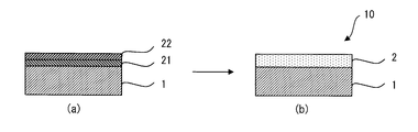
- the electromagnetic shielding metal foil 10 which concerns on the 1st Embodiment of this invention is the base material 1 which consists of metal foil, and the Sn alloy layer formed in the single side
- the substrate 1 may be anything as long as it is a highly conductive metal that exhibits an electromagnetic wave shielding effect. Examples of the substrate 1 include a foil of gold, silver, platinum, stainless steel, iron, nickel, zinc, copper, copper alloy, aluminum, or aluminum alloy, but a copper or aluminum foil is common.
- the formation method of the base material 1 is not specifically limited, For example, it may manufacture by rolling and you may form foil by electroplating.
- the substrate 1 may be formed by dry plating on the surface of a resin layer or resin film of an electromagnetic wave shielding material described later.
- the thickness of the substrate 1 is preferably determined in consideration of the frequency to be shielded by the electromagnetic wave and the skin effect. Specifically, it is preferable to set the skin depth to be equal to or greater than the skin depth obtained by substituting the conductivity of the elements constituting the substrate 1 and the target frequency into the following formula (1).
- the skin depth is 6.61 ⁇ m
- the thickness of the base material 1 is preferably about 7 ⁇ m or more.
- the thickness of the substrate 1 is more preferably 4 to 50 ⁇ m, further preferably 5 to 25 ⁇ m.
- d ⁇ 2 / (2 ⁇ ⁇ f ⁇ ⁇ ⁇ ⁇ ) ⁇ 1/2 (1)
- d Epidermis depth ( ⁇ m)
- f Frequency (GHz)
- ⁇ Conductivity of conductor (S / m)
- ⁇ Magnetic permeability of conductor (H / m)
- electrolytic copper foil is manufactured by electrolytically depositing copper on a titanium or stainless steel drum from a copper sulfate plating bath or a copper cyanide plating bath. Manufactured.
- oxygen-free copper JIS-H3100 (C1020)
- tough pitch copper JIS-H3100 (C1100)
- a copper alloy foil a well-known copper alloy can be used according to the required intensity
- Known copper alloys include, for example, 0.01-0.3% tin-containing copper alloys and 0.01-0.05% silver-containing copper alloys. -0.12% Sn and Cu-0.02% Ag are often used.
- a rolled copper foil having a conductivity of 5% or more can be used.
- a well-known thing can be used as an electrolytic copper foil.
- As the aluminum foil an aluminum foil having a purity of 99.0% or more can be used.
- a well-known aluminum alloy can be used according to the required intensity
- the Sn alloy layer is made of Ni, Cu or Ag, and Sn.
- the Sn alloy layer contains 20 to 80% by mass of Sn and has a thickness of 30 to 1500 nm. Note that the composition and thickness of the Sn alloy layer, the underlayer, and the Sn oxide can be measured by a STEM described later.
- the proportion of Sn in the Sn alloy layer is less than 20% by mass, the corrosion resistance of the Sn alloy layer decreases.
- the proportion of Sn exceeds 80% by mass the hardness of the Sn alloy layer decreases and becomes too soft, and Sn residue is generated.
- An alloy of Ni, Cu, or Ag and Sn has a lower contact resistance and higher corrosion resistance than other Sn alloys.
- the corrosion resistance is lowered, and when it exceeds 1500 nm, cracks and cracks are generated on the surface of the Sn alloy layer to expose the base, and the corrosion resistance is similarly inferior.
- the indentation hardness of the Sn alloy layer exceeds 500 MPa in accordance with ISO 14577-1, it is difficult to generate Sn residue, which is preferable.
- the indentation hardness of the Sn alloy layer is more preferably 1200 MPa or more, and further preferably 2000 MPa or more.
- the microindentation hardness of the Sn alloy layer is preferably 20000 MPa or less. If the hardness exceeds 20000 MPa, the Sn alloy layer may be cracked or cracked to expose the underlayer, resulting in poor corrosion resistance.
- ISO 14577-1 defines a method of ultra-fine indentation hardness test.
- the Sn alloy layer may further contain one or more elements selected from the group consisting of P, W, Fe, Co, and Zn. When the Sn alloy layer contains these elements, the layer can be hardened.
- the total proportion of the above elements in the Sn alloy layer is preferably 1 to 40% by mass, and more preferably 5 to 30% by mass.
- the Sn alloy layer can be formed by alloy plating (wet plating), sputtering using an alloy target constituting the alloy layer, vapor deposition using a component constituting the alloy layer, or the like. Further, as shown in FIG. 1A, for example, a first layer 21 made of an element other than Sn is first formed on one surface of the substrate 1, and a second layer 22 made of Sn is formed on the surface of the first layer 21. After the formation, the element of the first layer 21 can be diffused in the second layer 22 by heat treatment to form the Sn alloy layer 2 shown in FIG.
- the heat treatment conditions are not particularly limited. For example, the heat treatment can be performed at 120 to 500 ° C. for about 2 seconds to 10 hours.
- the metal foil 11 for electromagnetic wave shielding which concerns on the 2nd Embodiment of this invention is demonstrated.
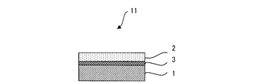
- the base layer 3 is further formed between the base material 1 and the Sn alloy layer 2 in the electromagnetic shielding metal foil 10 according to the first embodiment.
- the underlayer 3 prevents the diffusion of the element in the base material, and the ratio of Sn in the Sn alloy layer And it becomes easy to control the hardness of the Sn alloy layer.
- the underlayer 3 is composed of (1) a metal layer made of Cu, Ni or Ag, or (2) an alloy layer made of Ni, Cu or Ag and P, W, Fe, Co or Zn.
- An example of (2) is a Ni—Zn alloy layer.
- the underlayer 3 can be formed, for example, by increasing the thickness of the first layer 21 in FIG. 1A and leaving a part of the first layer 21 without the Sn alloy layer 2 after the heat treatment.
- the underlayer 3 and the Sn alloy layer 2 may be formed directly on the surface of the base material 1 by plating or the like in this order without heat treatment.
- the underlayer 3 and the Sn alloy layer 2 can also be formed by vapor deposition, PVD, CVD, etc., in addition to wet plating.
- a zinc substitution plating layer may be formed between the base layer 3 and the base material 1 as the base plating for electroplating the base layer 3.
- Sn oxide is formed on the surface of the Sn alloy layer.
- Sn oxide has high corrosion resistance.
- the corrosion resistance of the Sn alloy layer is further improved.
- FIG. 1A when the Sn alloy layer is formed by heating, Sn oxide is formed in the second layer 22 by natural oxidation when the second layer 22 made of Sn is formed, and thereafter Even in the alloying by heating, the Sn alloy layer remains.
- This Sn oxide has an effect of improving characteristics such as corrosion resistance.
- the Sn oxide does not have to be a layer and may be present on the surface of the Sn alloy layer, but a thickness of 2 to 30 nm is preferable.
- the contact resistance increases when the thickness of the layer exceeds 30 nm. Note that it is preferable to form the Sn alloy layer by heat treatment because a thick Sn oxide layer is positively formed during the heat treatment.
- the electromagnetic shielding material 100 is formed by laminating an electromagnetic shielding metal foil 10 and a resin layer or a resin film 4 on one surface of the metal foil 10.
- a resin such as polyimide can be used as the resin layer
- a film of PET (polyethylene terephthalate) or PEN (polyethylene naphthalate) can be used as the resin film.
- the resin layer and the resin film may be bonded to the metal foil with an adhesive, but the molten resin may be cast on the metal foil without using the adhesive, or the film may be thermocompression bonded to the metal foil.
- a film in which a copper or aluminum layer is directly formed on a resin film by PVD or CVD, or a thin layer of copper or aluminum is formed on a resin film by PVD or CVD as a conductive layer You may use the metallized film which formed the metal layer thickly by wet plating.
- a well-known thing can be used as a resin layer or a resin film.
- the thickness of the resin layer or the resin film is not particularly limited, but a resin layer having a thickness of, for example, 1 to 100 ⁇ m, more preferably 3 to 50 ⁇ m can be suitably used. When an adhesive is used, the thickness of the adhesive layer can be set to 10 ⁇ m or less, for example.
- the thickness of the electromagnetic shielding material 100 is preferably 1.0 mm or less, more preferably 0.01 to 0.5 mm.
- a shielded cable is obtained by winding the electromagnetic wave shielding material 100 around the outside of the cable.
- the aluminum foil As the aluminum foil, a 12 ⁇ m thick aluminum foil (manufactured by Sun Aluminum Industry Co., Ltd.) was used.
- the Al metallized film As the Al metallized film, a 12 ⁇ m-thick PET film (manufactured by Toyobo Co., Ltd.) with 6 ⁇ m of aluminum formed by vacuum deposition was used.
- Sn alloy layer An Sn alloy layer was formed on one side of the substrate.
- Table 1 shows a method for forming the Sn alloy layer.
- plating means that the first layer 21 and the second layer 22 were plated in this order by the method shown in FIG. 1A and then heat-treated at 150 to 180 ° C. for 2 to 7 hours in a nitrogen atmosphere. When the first layer 21 remained after the heat treatment, the composition is shown in Table 1 with the layer as an underlayer.
- Platinum only means that an Sn layer was formed by plating and no heat treatment was performed.
- alloy plating is the one in which an Sn alloy layer was formed by alloy plating, and the base layer was plated on the substrate before alloy plating.
- the Ni alloy plating shown in Table 1 was formed as an underlayer on one side of the base material, and then Sn plating was performed on the underlayer. Further, the Sn alloy layer was formed by heat treatment under the above conditions. Formed. At this time, elements other than Ni (P, W, Fe, Co) were also diffused from the base layer, and an Sn alloy layer containing three components was formed.
- a base Ni layer is formed on the Zn layer, a Sn plating is applied on the base Ni layer, and a Sn alloy layer is further formed by heat treatment. Formed.
- Example 20 in which the thickness of the Ni layer was reduced, Zn was also diffused from the Zn layer into the Sn layer on the surface, and a Sn—Ni—Zn alloy layer containing three components was formed.
- Comparative Example 8 after a Zn layer was formed on the aluminum foil by displacement plating, a base Ni layer was plated on the Zn layer, and Sn plating was applied on the base Ni layer.
- Ni plating Ni sulfate bath (Ni concentration: 20 g / L, current density: 2 to 10 A / dm 2 )
- Sn plating phenol sulfonic acid Sn bath (Sn concentration: 40 g / L, current density: 2 to 10 A / dm 2 )
- Cu plating Cu sulfate bath (Cu concentration: 20 g / L, current density: 2 to 10 A / dm 2 )
- Zn displacement plating zincate bath (Zn concentration: 15 g / L)
- Ni—Sn plating: pyrophosphate bath Ni concentration 10 g / L, Sn concentration 10 g / L, current density: 0.1 to 2 A / dm 2
- Co—Sn plating pyrophosphate bath (Co concentration 20 g
- Ni-P sulfuric acid bath (Ni concentration: 20 g / L, P concentration: 20 g / L, current density: 2-4 A / dm 2 )
- Ni—W sulfuric acid bath (Ni concentration: 20 g / L, W concentration: 20 g / L, current density: 0.1 to 2 A / dm 2 )
- Ni—Fe sulfuric acid bath (Ni concentration: 20 g / L, Fe concentration: 10 g / L, current density: 0.1 to 2 A / dm 2 )
- Ni—Co sulfuric acid bath (Ni concentration: 20 g / L, Co concentration: 10 g / L, current density: 0.1 to 2 A / dm 2 )
- “Sputtering” is a heat treatment after sputtering of Ni and Sn in this order.
- alloy sputtering is an alloy layer formed by sputtering using a target material of a corresponding alloy.
- the layer formed by alloy sputtering has the composition of the alloy layer itself, no heat treatment was performed. Sputtering and alloy sputtering were performed under the following conditions.
- Sputtering equipment Batch type sputtering equipment (ULVAC, Model MNS-6000) Sputtering conditions: ultimate vacuum 1.0 ⁇ 10 ⁇ 5 Pa, sputtering pressure 0.2 Pa, sputtering power 50 W
- Vapor deposition equipment Vacuum vapor deposition equipment (ULVAC, model MB05-1006) Deposition conditions: ultimate vacuum 5.0 ⁇ 10 ⁇ 3 Pa, electron beam acceleration voltage 6 kV Deposition source: Ni (purity 3N)
- the cross-sectional sample of the obtained metal foil for electromagnetic wave shielding was subjected to line analysis by STEM (scanning transmission electron microscope, JEM-2100F manufactured by JEOL Ltd.) to determine the layer configuration.
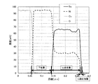
- the analyzed designated elements are Sn, Ag, Ni, Cu, P, W, Fe, Co, Zn, C, S and O. Further, the ratio (wt%) of each element in each layer was analyzed with the total of the specified elements described above being 100% (acceleration voltage: 200 kV, measurement interval: 2 nm). As shown in FIG.
- a layer containing 5 wt% or more of Sn and containing 5 wt% or more of any element of Ag, Ni, and Cu is an Sn alloy layer, and the thickness is shown in FIG. Response).
- a layer that is located on the lower layer side of the Sn alloy layer and has Sn of less than 5 wt% and containing any element of Ag, Ni, and Cu in an amount of 5 wt% or more was used as a base layer, and the thickness thereof was determined on the drawing.
- the layer located on the upper layer side from the Sn alloy layer and having Sn of 5 wt% or more and O of 5 wt% or more was defined as an Sn oxide layer, and the thickness thereof was determined on the drawing.
- the STEM measurement was performed in 3 fields of view, and the average value of 3 fields ⁇ 5 locations was defined as the thickness of each layer.
- composition of Sn alloy layer and underlayer The composition of the Sn alloy layer and the underlayer was determined by line analysis using STEM (scanning transmission electron microscope). The elements constituting the Sn alloy layer and the underlayer were designated elements, and the mass ratio of each element when the total of the designated elements was 100% was defined as the composition of the Sn alloy layer and the underlayer. (Measurement of hardness) The surface of the obtained metal foil for electromagnetic wave shielding on the Sn alloy layer side was measured for hardness by an ultra-fine indentation hardness test in accordance with ISO14577-1. ENT-2100 made by Elionix was used for the measurement of hardness.
- the surface on the alloy layer side of the obtained metal foil for electromagnetic shielding was subjected to a salt spray test, and the contact resistance of the outermost surface on the Sn alloy layer side before and after the test was measured.
- the contact resistance was measured by a four-terminal method using an electrical contact simulator CRS-1 manufactured by Yamazaki Seiki Co., Ltd. Probe: gold probe, contact load: 20 gf, bias current: 10 mA, sliding distance: 1 mm
- the salt spray test was in accordance with JIS-Z2371 (temperature: 35 ° C., salt water component: sodium chloride, salt water concentration: 5 wt%, spray pressure: 98 ⁇ 10 kPa, spray time: 48 h).
- the initial contact resistance before the salt spray test indicates the evaluation of the contact resistance itself, and the contact resistance after the salt spray test indicates the evaluation of corrosion resistance.
- ⁇ Contact resistance is less than 20 m ⁇ ⁇ : Contact resistance is 20 m ⁇ or more, less than 100 m ⁇ ⁇ : Contact resistance is 100 m ⁇ or more
- each of the examples has an Sn alloy layer comprising Cu, Ni or Ag and Sn on the surface of the base material, containing 20 to 80% by mass of Sn and having a thickness of 30 to 1500 nm.
- the contact resistance was low, the corrosion resistance was excellent, and Sn residue was hardly generated.
- the corrosion resistance was more excellent in Examples 1 to 12 and 16 to 20 where the Sn oxide layer was thicker than the other examples.
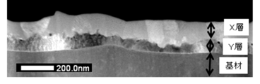
- 4 and 5 show a cross-sectional image of the sample of Example 1 by STEM and the result of line analysis by STEM, respectively.
- the X layer and Y layer in the cross-sectional image are found to be a Ni—Sn alloy layer (Sn alloy layer) and a Ni layer (underlayer) from the results of the line analysis, respectively.
- Comparative Example 5 In Comparative Example 5 in which the Sn—Co layer was formed as the Sn alloy layer, Sn debris was hardly generated, but the contact resistance was high and the corrosion resistance was poor.
- Comparative Examples 6 to 8 in which a pure Sn layer was provided instead of the Sn alloy layer, the Sn layer had a hardness of 500 MPa or less, and Sn residue was remarkably generated.
- Comparative Example 9 in which the Ni layer was formed instead of the Sn alloy layer, the corrosion resistance was inferior.
- Comparative Example 10 in which the Sn ratio in the Sn alloy layer was less than 20% by mass, the contact resistance was high and the corrosion resistance was inferior. Further, the Sn alloy layer had a hardness of 500 MPa or less, and Sn residue was remarkably generated.
Landscapes
- Chemical & Material Sciences (AREA)
- Engineering & Computer Science (AREA)
- Chemical Kinetics & Catalysis (AREA)
- Materials Engineering (AREA)
- Metallurgy (AREA)
- Organic Chemistry (AREA)
- Electrochemistry (AREA)
- Mechanical Engineering (AREA)
- Microelectronics & Electronic Packaging (AREA)
- Laminated Bodies (AREA)
Abstract
L'invention concerne une feuille métallique destinée au blindage contre les ondes électromagnétiques et qui présente une faible résistance de contact, une résistance supérieure à l'humidité et une résistance supérieure à la corrosion, et ne génère pas facilement de Sn gazeux; un élément de blindage contre les ondes électromagnétiques et un câble blindé. Dans cette feuille métallique (10) de blindage contre les ondes électromagnétiques, une couche d'alliage de Sn (2) comprenant Cu, Ni ou Ag, et Sn, est formée sur une face ou sur les deux faces d'un substrat comprenant une feuille métallique (1) dont l'épaisseur est de 100 µm au maximum; et la couche d'alliage de Sn contient 20-80 % en masse de Sn et présente une épaisseur de 30-1500 nm.
Priority Applications (1)
| Application Number | Priority Date | Filing Date | Title |
|---|---|---|---|
| PCT/JP2014/064473 WO2015181969A1 (fr) | 2014-05-30 | 2014-05-30 | Feuille metallique de blindage contre les ondes electromagnetiques, element de blindage contre les ondes electromagnetiques et cable blinde |
Applications Claiming Priority (1)
| Application Number | Priority Date | Filing Date | Title |
|---|---|---|---|
| PCT/JP2014/064473 WO2015181969A1 (fr) | 2014-05-30 | 2014-05-30 | Feuille metallique de blindage contre les ondes electromagnetiques, element de blindage contre les ondes electromagnetiques et cable blinde |
Publications (1)
| Publication Number | Publication Date |
|---|---|
| WO2015181969A1 true WO2015181969A1 (fr) | 2015-12-03 |
Family
ID=54698343
Family Applications (1)
| Application Number | Title | Priority Date | Filing Date |
|---|---|---|---|
| PCT/JP2014/064473 Ceased WO2015181969A1 (fr) | 2014-05-30 | 2014-05-30 | Feuille metallique de blindage contre les ondes electromagnetiques, element de blindage contre les ondes electromagnetiques et cable blinde |
Country Status (1)
| Country | Link |
|---|---|
| WO (1) | WO2015181969A1 (fr) |
Citations (8)
| Publication number | Priority date | Publication date | Assignee | Title |
|---|---|---|---|---|
| JP3069015U (ja) * | 1999-02-02 | 2000-05-30 | 帝人株式会社 | 電磁波遮蔽材 |
| JP2003201597A (ja) * | 2002-01-09 | 2003-07-18 | Nippon Denkai Kk | 銅箔とその製造方法及び該銅箔を用いた電磁波シールド体 |
| JP2008274417A (ja) * | 2007-03-30 | 2008-11-13 | Nikko Kinzoku Kk | 積層銅箔及びその製造方法 |
| JP2011086786A (ja) * | 2009-10-16 | 2011-04-28 | Bridgestone Corp | 光透過性電磁波シールド材の製造方法、及び光透過性電磁波シールド材 |
| WO2013105520A1 (fr) * | 2012-01-13 | 2013-07-18 | Jx日鉱日石金属株式会社 | Composite de feuille de cuivre, corps formé, et procédé de fabrication associé |
| WO2013105266A1 (fr) * | 2012-01-13 | 2013-07-18 | Jx日鉱日石金属株式会社 | Composite de feuille de cuivre, corps moulé, et procédé de production associé |
| WO2013105265A1 (fr) * | 2012-01-13 | 2013-07-18 | Jx日鉱日石金属株式会社 | Composite de feuille de cuivre, corps moulé, et procédé de production associé |
| JP5497949B1 (ja) * | 2013-07-03 | 2014-05-21 | Jx日鉱日石金属株式会社 | 電磁波シールド用金属箔、電磁波シールド材及びシールドケーブル |
-
2014
- 2014-05-30 WO PCT/JP2014/064473 patent/WO2015181969A1/fr not_active Ceased
Patent Citations (8)
| Publication number | Priority date | Publication date | Assignee | Title |
|---|---|---|---|---|
| JP3069015U (ja) * | 1999-02-02 | 2000-05-30 | 帝人株式会社 | 電磁波遮蔽材 |
| JP2003201597A (ja) * | 2002-01-09 | 2003-07-18 | Nippon Denkai Kk | 銅箔とその製造方法及び該銅箔を用いた電磁波シールド体 |
| JP2008274417A (ja) * | 2007-03-30 | 2008-11-13 | Nikko Kinzoku Kk | 積層銅箔及びその製造方法 |
| JP2011086786A (ja) * | 2009-10-16 | 2011-04-28 | Bridgestone Corp | 光透過性電磁波シールド材の製造方法、及び光透過性電磁波シールド材 |
| WO2013105520A1 (fr) * | 2012-01-13 | 2013-07-18 | Jx日鉱日石金属株式会社 | Composite de feuille de cuivre, corps formé, et procédé de fabrication associé |
| WO2013105266A1 (fr) * | 2012-01-13 | 2013-07-18 | Jx日鉱日石金属株式会社 | Composite de feuille de cuivre, corps moulé, et procédé de production associé |
| WO2013105265A1 (fr) * | 2012-01-13 | 2013-07-18 | Jx日鉱日石金属株式会社 | Composite de feuille de cuivre, corps moulé, et procédé de production associé |
| JP5497949B1 (ja) * | 2013-07-03 | 2014-05-21 | Jx日鉱日石金属株式会社 | 電磁波シールド用金属箔、電磁波シールド材及びシールドケーブル |
Similar Documents
| Publication | Publication Date | Title |
|---|---|---|
| JP5497949B1 (ja) | 電磁波シールド用金属箔、電磁波シールド材及びシールドケーブル | |
| JP5774061B2 (ja) | 電磁波シールド用金属箔、電磁波シールド材及びシールドケーブル | |
| JP5887305B2 (ja) | 電磁波シールド用金属箔、電磁波シールド材、及びシールドケーブル | |
| WO2014199547A1 (fr) | Procédé de production de stratifié plaqué, et stratifié plaqué | |
| WO2017090638A1 (fr) | Matériau de borne en cuivre étamé, borne, et structure de partie terminale de fil électrique | |
| TW201718949A (zh) | Sn鍍敷材及其製造方法 | |
| WO2015181970A1 (fr) | Feuille métallique pour blindage vis-à-vis des ondes électromagnétiques, élément de blindage vis-à-vis des ondes électromagnétiques, et câble blindé | |
| JP5534627B1 (ja) | 電磁波シールド用金属箔、電磁波シールド材及びシールドケーブル | |
| JP2021075772A (ja) | 電気接点用材料およびその製造方法、コネクタ端子、コネクタならびに電子部品 | |
| CN106414811A (zh) | 电触点材料、电触点材料的制造方法和端子 | |
| JP6086531B2 (ja) | 銀めっき材 | |
| JP5619307B1 (ja) | 電磁波シールド用金属箔、電磁波シールド材及びシールドケーブル | |
| WO2018124115A1 (fr) | Matériau de traitement de surface et article fabriqué à l'aide dudit matériau | |
| JP5534626B1 (ja) | 電磁波シールド用金属箔、電磁波シールド材及びシールドケーブル | |
| KR20130124383A (ko) | 조화 처리면을 구비한 압연 구리 또는 구리 합금박 | |
| WO2015181969A1 (fr) | Feuille metallique de blindage contre les ondes electromagnetiques, element de blindage contre les ondes electromagnetiques et cable blinde | |
| JP5887287B2 (ja) | 電磁波シールド用金属箔及び電磁波シールド材 | |
| JP2008196010A (ja) | コネクタ端子用めっき材料 | |
| JP5887283B2 (ja) | 電磁波シールド用金属箔及び電磁波シールド材 |
Legal Events
| Date | Code | Title | Description |
|---|---|---|---|
| 121 | Ep: the epo has been informed by wipo that ep was designated in this application |
Ref document number: 14893327 Country of ref document: EP Kind code of ref document: A1 |
|
| NENP | Non-entry into the national phase |
Ref country code: DE |
|
| NENP | Non-entry into the national phase |
Ref country code: JP |
|
| 122 | Ep: pct application non-entry in european phase |
Ref document number: 14893327 Country of ref document: EP Kind code of ref document: A1 |