WO2015182531A1 - 熱式流量計 - Google Patents
熱式流量計 Download PDFInfo
- Publication number
- WO2015182531A1 WO2015182531A1 PCT/JP2015/064844 JP2015064844W WO2015182531A1 WO 2015182531 A1 WO2015182531 A1 WO 2015182531A1 JP 2015064844 W JP2015064844 W JP 2015064844W WO 2015182531 A1 WO2015182531 A1 WO 2015182531A1
- Authority
- WO
- WIPO (PCT)
- Prior art keywords
- circuit
- flow meter
- signal
- delay
- switching
- Prior art date
- Legal status (The legal status is an assumption and is not a legal conclusion. Google has not performed a legal analysis and makes no representation as to the accuracy of the status listed.)
- Ceased
Links
Images




Classifications
-
- H—ELECTRICITY
- H03—ELECTRONIC CIRCUITRY
- H03K—PULSE TECHNIQUE
- H03K4/00—Generating pulses having essentially a finite slope or stepped portions
- H03K4/94—Generating pulses having essentially a finite slope or stepped portions having trapezoidal shape
-
- G—PHYSICS
- G01—MEASURING; TESTING
- G01F—MEASURING VOLUME, VOLUME FLOW, MASS FLOW OR LIQUID LEVEL; METERING BY VOLUME
- G01F1/00—Measuring the volume flow or mass flow of fluid or fluent solid material wherein the fluid passes through a meter in a continuous flow
- G01F1/68—Measuring the volume flow or mass flow of fluid or fluent solid material wherein the fluid passes through a meter in a continuous flow by using thermal effects
- G01F1/696—Circuits therefor, e.g. constant-current flow meters
- G01F1/698—Feedback or rebalancing circuits, e.g. self heated constant temperature flowmeters
-
- H—ELECTRICITY
- H03—ELECTRONIC CIRCUITRY
- H03K—PULSE TECHNIQUE
- H03K17/00—Electronic switching or gating, i.e. not by contact-making and –breaking
- H03K17/16—Modifications for eliminating interference voltages or currents
-
- H—ELECTRICITY
- H03—ELECTRONIC CIRCUITRY
- H03K—PULSE TECHNIQUE
- H03K17/00—Electronic switching or gating, i.e. not by contact-making and –breaking
- H03K17/16—Modifications for eliminating interference voltages or currents
- H03K17/161—Modifications for eliminating interference voltages or currents in field-effect transistor switches
- H03K17/162—Modifications for eliminating interference voltages or currents in field-effect transistor switches without feedback from the output circuit to the control circuit
-
- H—ELECTRICITY
- H03—ELECTRONIC CIRCUITRY
- H03K—PULSE TECHNIQUE
- H03K17/00—Electronic switching or gating, i.e. not by contact-making and –breaking
- H03K17/16—Modifications for eliminating interference voltages or currents
- H03K17/161—Modifications for eliminating interference voltages or currents in field-effect transistor switches
- H03K17/162—Modifications for eliminating interference voltages or currents in field-effect transistor switches without feedback from the output circuit to the control circuit
- H03K17/163—Soft switching
- H03K17/164—Soft switching using parallel switching arrangements
-
- H—ELECTRICITY
- H03—ELECTRONIC CIRCUITRY
- H03K—PULSE TECHNIQUE
- H03K17/00—Electronic switching or gating, i.e. not by contact-making and –breaking
- H03K17/28—Modifications for introducing a time delay before switching
- H03K17/284—Modifications for introducing a time delay before switching in field effect transistor switches
-
- H—ELECTRICITY
- H03—ELECTRONIC CIRCUITRY
- H03K—PULSE TECHNIQUE
- H03K19/00—Logic circuits, i.e. having at least two inputs acting on one output; Inverting circuits
- H03K19/0175—Coupling arrangements; Interface arrangements
-
- H—ELECTRICITY
- H03—ELECTRONIC CIRCUITRY
- H03K—PULSE TECHNIQUE
- H03K4/00—Generating pulses having essentially a finite slope or stepped portions
- H03K4/06—Generating pulses having essentially a finite slope or stepped portions having triangular shape
Definitions
- the present invention relates to a thermal flow meter.
- the thermal flow meter is a sensor that measures the flow rate of the air that has flowed based on the current required to restore the temperature of the hot wire changed by the air flowing around it.
- the measured flow rate can be represented by a periodic signal having a frequency corresponding to the flow rate, for example.
- the periodic signal is input to, for example, an open drain circuit (or an open collector circuit, the same applies hereinafter), and the flow rate can be detected by measuring the frequency of the signal output from the open drain circuit using a frequency measurement circuit.
- the open drain circuit outputs a high level / low level output signal by turning on / off the switching element.
- By turning ON / OFF the switching element according to the frequency of the periodic signal an output signal corresponding to the flow rate represented by the frequency of the periodic signal can be output.
- Patent Document 1 describes a specific example of an open drain circuit in which switching timing of each switching element is different.
- the frequency of the periodic signal input to the open drain circuit changes according to the measured flow rate. Therefore, when the frequency of the periodic signal is increased, the ON / OFF cycle of the switching element of the open drain circuit is shortened.
- the delay time interval between switching elements is constant. Therefore, when the frequency of the periodic signal becomes higher than a certain level, for example, the first-stage switching element starts the operation of the next period before the final-stage switching element operates, and the output signal changes from High level to Low level within one period. It may not be possible to change. In this case, it is difficult to accurately detect the flow rate represented by the frequency of the periodic signal.
- the present invention has been made in view of the problems as described above.
- a thermal type flow meter that represents the air flow rate by the frequency of a periodic signal, the waveform abnormality of the output signal due to the frequency change while suppressing high frequency noise.
- the purpose is to avoid.
- the thermal flow meter according to the present invention includes a plurality of switching elements connected in parallel, and changes a delay width between the switching elements in accordance with a frequency change of a periodic signal representing a flow rate.
- the peak value or frequency of the output signal becomes an abnormal value even if the frequency of the periodic signal changes while suppressing high frequency noise by a plurality of switching elements connected in parallel. Can be suppressed,
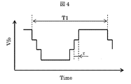
- FIG. 4 is a waveform diagram of an output signal when a pulse signal having a cycle of T1 is input to the open drain circuit of FIG.
- FIG. 4 is a waveform diagram of an output signal when a pulse signal having a period T2 shorter than T1 is input to the open drain circuit of FIG. 3.
- FIG. 4 is a waveform diagram of an output signal when a pulse signal having a period T2 shorter than T1 is input to the open drain circuit of FIG. 3.
- FIG. 4 is a waveform diagram of an output signal when a pulse signal having a period T3 ( ⁇ 4 ⁇ ) is input to the open drain circuit of FIG. 3.
- 1 is a circuit diagram of an open drain circuit 1 according to Embodiment 1.
- FIG. It is a wave form diagram of input signal Vi. 2 is a diagram illustrating a configuration example of a frequency measurement circuit 2 connected to an open drain circuit 1.
- FIG. FIG. 10 is a waveform diagram of an output voltage Vfo when a triangular wave input signal Vi is input to the open drain circuit 1 in the circuit configuration of FIG. 9.
- the waveform of the output voltage Vfo when the cycle of the input signal Vi changes in the circuit configuration of FIG. This is a waveform example in which the output signal Vfo does not cross the comparison voltage Vc.
- FIG. 3 is a circuit diagram of an open drain circuit 1 according to Embodiment 2.
- FIG. 3 shows a circuit configuration in which the current limiting resistor connected to the drain terminal of the transistor Tr3 is removed and the output terminal Fo is short-circuited in the conventional open drain circuit shown in FIG. It is an output signal waveform of the open drain circuit of FIG. It is a figure which shows the output signal waveform of the open drain circuit 1 which concerns on Embodiment 3.
- FIG. FIG. 10 is a diagram showing a modification of the open drain circuit 1 according to the third embodiment. It is an example of the output signal waveform in the circuit structure of FIG. It is a block diagram of the thermal type flow meter 100 which concerns on Embodiment 4.
- FIG. 3 shows a circuit configuration in which the current limiting resistor connected to the drain terminal of the transistor Tr3 is removed and the output terminal Fo is short-circuited in the conventional open drain circuit shown in FIG. It is an output signal waveform of the open drain circuit of FIG. It is a figure which shows the output
- Measures against radiation electromagnetic waves generated when an output signal representing information by frequency is output from an open collector circuit include the following.
- FIG. 1 shows an example of an output signal waveform when electromagnetic wave noise is suppressed using a low-pass filter.
- a low-pass filter configured by combining an inductor, a capacitor, and a resistor is arranged.
- a steep voltage change occurs at the beginning and the beginning of the decrease of the output signal voltage, and the output signal includes a high frequency component.
- the waveform when the voltage V decreases is expressed by the following equation 1, and the waveform when the voltage V increases is expressed by the following equation 2.
- A is a peak value
- ⁇ is a time constant
- ⁇ is a constant
- V A * Exp (- ⁇ * t) + ⁇ Equation 1
- V A * (1-Exp (- ⁇ * t)) + ⁇
- FIG. 2 is an example of an output signal waveform when a current flowing through an open drain circuit is limited using a current mirror circuit. In this case, as shown in FIG. 2, when the voltage increases, current limitation cannot be applied.
- the ideal waveform for the periodic signal is a sine wave.
- the transistor at the output end is turned ON / OFF, and the voltage of the output signal is received from an external power supply. Therefore, the signal waveform output from the open drain circuit is a rectangular wave in principle.
- Equation 3 represents the current waveform that flows into the output terminal of the open drain circuit.
- a magnetic field H represented by the following formula 4 is generated around I. r is the distance from the current.
- the relationship between the magnetic field H and the electric field E is expressed by the following formula 5 according to Maxwell's equation.
- ⁇ magnetic permeability and t is time. Therefore, when a rectangular wave current flows, a high-frequency electromagnetic wave is emitted even if the frequency is low, and the peripheral device is affected by noise.
- FIG. 3 is a circuit diagram showing an example of an open drain circuit in which a time difference is given to the timing of switching by a delay circuit as described in Patent Document 1.
- three open drain transistors each having a current limiting resistor connected to the drain terminal are connected in parallel to the output terminal.
- a delay circuit D having a delay time ⁇ is disposed between the gates of the three open drain transistors Tr1, Tr2, Tr3.
- the source terminals of the open drain transistors Tr1 to Tr3 are grounded.
- the drain terminals of the open drain transistors Tr1 to Tr3 are connected to the output terminal Fo.
- a pull-up resistor Rp is connected to the drain terminal, and the output signal is pulled up by the voltage Vp.
- the open drain transistors Tr1 to Tr3 are controlled by inputting a pulse signal (Signal Pulse) which is a periodic signal to the gate terminal.
- a pulse signal for turning on the open drain transistors Tr1 to Tr3 is input, Tr1 is turned on first, Tr2 is turned on with a delay of ⁇ , and Tr3 is turned on with a delay of ⁇ .
- Tr1 becomes non-conductive
- Tr2 becomes non-conductive after a delay of ⁇
- Tr3 becomes non-conductive after a delay of ⁇ .
- FIG. 4 is a waveform diagram of an output signal when a pulse signal having a period T1 is input to the open drain circuit of FIG.
- the output voltage Vfo decreases each time a current flows through the open drain transistors Tr1 to Tr3, and the output voltage Vfo increases each time the open drain transistors Tr1 to Tr3 flow.
- the cycle of the output signal is the same T1 as the pulse signal.
- FIG. 5 is a waveform diagram of an output signal when a pulse signal having a period T2 shorter than T1 is input to the open drain circuit of FIG. Compared with FIG. 4, since the delay time ⁇ does not change, the time interval at which each transistor switches between conducting and non-conducting is the same, but the waveform period is shorter than in FIG.
- FIG. 6 is a waveform diagram of an output signal when a pulse signal having a period T3 ( ⁇ 4 ⁇ ) is input to the open drain circuit of FIG.
- Tr1 performs the switching operation of the next period before Tr3 operates. Accordingly, the open drain transistors Tr1 to Tr3 do not all become the same operation state (conductive or non-conductive), so that the signal waveform cannot reach the upper limit (Hi level) and the lower limit (Low level). That is, the peak value of the output signal becomes small, the period is shorter than T3, and is not a constant period.
- the present invention provides an output as shown in FIG. 6 in an open drain circuit in which a plurality of switching elements are connected in parallel to an output terminal and a steep change in waveform is suppressed by providing a time difference in the operation timing of each switching element.
- the object is to avoid abnormal signal waveforms.
- FIG. 7 is a circuit diagram of the open drain circuit 1 according to the first embodiment of the present invention.
- three open drain transistors Tr1 to Tr3 are connected to the output terminal Fo via current limiting resistors Rd1 to Rd3, respectively.
- An input signal Vi for driving the transistors Tr1 to Tr3 is input to the input terminal Vi.
- the voltages Vg1 to Vg3 obtained by dividing the input signal Vi by the voltage dividing resistors Rg1 to Rg4 are input to the gate terminals of the transistors Tr1 to Tr3, respectively.
- the relationship between Vi and Vg1 to Vg3 is expressed by the following equations 6 to 8.
- Vg1 Vi * (Rg2 + Rg3 + Rg4) / (Rg1 + Rg2 + Rg3 + Rg4) Equation 6
- Vg2 Vi * (Rg3 + Rg4) / (Rg1 + Rg2 + Rg3 + Rg4) Equation 7
- Vg3 Vi * Rg4 / (Rg1 + Rg2 + Rg3 + Rg4) ⁇ ⁇ ⁇ Formula 8
- FIG. 8 is a waveform diagram of the input signal Vi.
- a triangular wave is used as an example.
- the transistors Tr1 to Tr3 reach the threshold value Vth at different voltage values of the triangular wave. Therefore, each transistor switches at a different time.
- FIG. 9 is a diagram illustrating a configuration example of the frequency measurement circuit 2 connected to the open drain circuit 1.
- the frequency measuring circuit 2 includes a frequency measuring device 3, a pull-up power source Vp, and a pull-up resistor Rp.
- the input terminal Input of the frequency measuring device 3 is connected to the output terminal Fo of the open drain circuit 1 and further connected to the pull-up power supply Vp via the pull-up resistor Rp.
- FIG. 10 is a waveform diagram of the output voltage Vfo when the triangular wave input signal Vi is input to the open drain circuit 1 in the circuit configuration of FIG. Each transistor is switched when the input signal Vi becomes a value represented by Equation 9 to Equation 11, respectively. Therefore, the output voltage Vfo changes stepwise as shown in FIG.
- the output voltage Vfo when the Tr1 to Tr3 is in a non-conductive state is Vfo0
- the output voltage Vfo when the Tr1 is in a conductive state and the Tr2 and Tr3 are in a non-conductive state is Vfo2
- the output voltage Vfo at that time is Vfo2
- the output voltage Vfo when Tr1 to Tr3 is in a conducting state is Vfo3.
- Vfo0 Vp Equation 12
- Vfo1 Vp * Rd1 / (Rd1 + Rp) Equation 13
- Vfo2 Vp * Rd12 / (Rd12 + Rp) (14)
- Vfo3 Vp * Rd123 / (Rd123 + Rp) Equation 15
- Rd12 in Expression 14 is a combined resistance in which Rd1 and Rd2 are connected in parallel, and is expressed by Expression 16 below.
- Rd123 in Expression 15 is a combined resistance in which Rd1 to Rd3 are connected in parallel, and is expressed by Expression 17 below.
- Rd12 Rd1 * Rd2 / (Rd1 + Rd2) Equation 16
- Rd123 Rd1 * Rd2 * Rd3 / (Rd1 * Rd2 + Rd2 * Rd3 + Rd3 * Rd1) Equation 17
- FIG. 11 shows a waveform of the output voltage Vfo when the cycle of the input signal Vi changes in the circuit configuration of FIG.
- ⁇ 1 be the time difference in switching timing between the transistors when the cycle of Vi is T1
- ⁇ 2 be the time difference in switching timing when the cycle of Vi is T2.
- T1 / T2 ⁇ 1 / ⁇ 2 Equation 18
- the open drain circuit 1 includes the delay circuit (the voltage dividing circuit in the first embodiment) that shifts the timing for switching the transistors Tr1 to Tr3 for each transistor.
- the delay circuit changes the delay time interval ⁇ between the transistors according to the frequency of the input signal Vi to the open drain circuit 1. Therefore, when the cycle of the input signal Vi is shortened, the delay time interval ⁇ is also shortened accordingly, so that the waveform abnormality of the output signal as shown in FIG. 6 can be suppressed. That is, when the information is represented by the frequency of the input signal Vi and the frequency measurement circuit 2 acquires the information by measuring the frequency, the measurement abnormality as shown in FIG. 6 can be suppressed.
- the voltages Vfo1 to Vfo3 when the output voltage Vfo is switched stepwise are divided by the pullup resistor Rp and the current limiting resistors Rd1 to Rd3. It is a thing.
- the pull-up resistor Rp and the current limiting resistors Rd1 to Rd3 are often manufactured by a semiconductor process. Resistors manufactured by a semiconductor process have variations in resistance values, and may reach, for example, about ⁇ 20%. Also, the temperature characteristics of the resistance value vary.
- the pull-up resistor Rp and the current limiting resistors Rd1 to Rd3 often vary in resistance value ratio and resistance value temperature characteristic ratio for each product. If there is such resistance value variation, the following problems occur in actual products.
- the frequency measuring device 3 measures the frequency and period of the output signal Vfo by measuring the time when the magnitude relationship between Vfo and Vc is switched.
- FIG. 12 shows a waveform example in which the output signal Vfo does not cross the comparison voltage Vc.
- the frequency measuring device 3 cannot measure the frequency of the output signal Vfo.
- Equations 13 to 15 if the resistance values of the current limiting resistors Rd1 to Rd3 vary with respect to the resistance value of the pull-up resistor Rp, Vfo1 to Vfo3 also increase accordingly. There is a possibility that a state as shown in FIG. In the second embodiment of the present invention, a circuit example that addresses such a problem will be described.
- FIG. 13 is a circuit diagram of the open drain circuit 1 according to the second embodiment.
- the open drain circuit 1 of FIG. 13 is obtained by short-circuiting the drain terminal of the transistor Tr3 with the output terminal Fo without providing the current limiting resistor Rd3 in the circuit configuration shown in FIG.
- the output voltage Vfo becomes 0 (V). Therefore, Vfo can be a potential lower than Vc irrespective of variations in resistance values of the pull-up resistor Rp and the current limiting resistors Rd1 to Rd3.
- FIG. 14 shows a circuit configuration in which the current limiting resistance connected to the drain terminal of the transistor Tr3 is removed and the output terminal Fo is short-circuited in the conventional open drain circuit shown in FIG.
- the drain terminal of the transistor Tr3 and the output terminal Fo are short-circuited as in the second embodiment, the following problems occur.
- the order in which the transistors Tr1 to Tr3 are switched from non-conduction to conduction is the same as the order in which the transistors Tr1 to Tr3 are switched from conduction to non-conduction. That is, in any case, Tr1 is switched first and Tr3 is switched last.
- FIG. 15 shows an output signal waveform of the open drain circuit of FIG.
- the output waveform switches from a low potential (Low level) to a high potential (High level)
- the waveform does not change stepwise but switches in one stage.
- the output waveform is switched sharply in this way, the effect of reducing the radiation noise is diminished.
- Tr3 without a current limiting resistor is switched last, and from conduction to non-conduction.
- the switching order may be as long as Tr3 without a current limiting resistor is switched first.
- the order in which the open drain transistors Tr1 to Tr3 are switched from non-conduction to conduction is opposite to the order in which the open drain transistors Tr1 to Tr3 are switched from conduction to non-conduction.
- Tr3 is switched last when switching from non-conduction to conduction, and Tr3 is switched first when switching from conduction to non-conduction. Therefore, in the open drain circuit 1 according to the first and second embodiments, a steep change in the output waveform shown in FIG. 15 can be suppressed.
- the open drain circuit 1 according to the second embodiment can suppress the problem as shown in FIG. 12 caused by the resistance value variation of the pull-up resistor Rp and the current limiting resistors Rd1 to Rd3. Furthermore, a steep output change as shown in FIG. 15 when a similar configuration is adopted in a conventional open drain circuit can be suppressed.
- the drain terminal of Tr3 is short-circuited with the output terminal Fo, but other transistors may be short-circuited in the same manner.
- the drain terminal of Tr2 and the output terminal Fo may be short-circuited.
- FIG. 16 is a diagram illustrating an output signal waveform of the open drain circuit 1 according to the third embodiment of the present invention.
- a plurality of time differences ⁇ of switching timing between the open drain transistors are set.
- the time difference between Tr1 and Tr2 is ⁇ 1
- the time difference between Tr2 and Tr3 is ⁇ 2. Since ⁇ 1 and ⁇ 2 are determined according to Equations 9 to 11, ⁇ 1 and ⁇ 2 can be adjusted as shown in FIG. 16 by adjusting the voltage dividing ratio by the voltage dividing resistors Rg1 to Rg4.
- the delay time interval ( ⁇ 1) of the switching element that switches first is the delay time interval of the switching element that switches later. It is smaller than ( ⁇ 2).
- the delay time interval ( ⁇ 2) of the switching element that switches first is larger than the delay time interval ( ⁇ 1) of the switching element that switches later. That is, both ⁇ 1 and ⁇ 2 are constant.
- FIG. 17 is a view showing a modification of the open drain circuit 1 according to the third embodiment.
- the open drain circuit 1 shown in FIG. 17 includes a microcomputer 4 that realizes this.
- the microcomputer 4 receives the input signal Vi, operates the desired timing for switching each transistor in accordance with Vi, and outputs Vth to the gate terminal of each transistor at that timing.
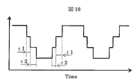
- FIG. 18 is an example of an output signal waveform in the circuit configuration of FIG.
- the delay time interval ( ⁇ 1) of the switching element that switches first is later than the delay time interval ( ⁇ 2 of the switching element that switches later. Smaller than).
- the delay time interval ( ⁇ 2) of the switching element that switches first is smaller than the delay time interval ( ⁇ 1) of the switching element that switches later. That is, ⁇ 1 and ⁇ 2 change with time.
- a capacitor, a resistor, a diode, or the like may be provided as a surge protection element or a protection element from electrostatic discharge.
- a plurality of switching time differences may be required as shown in FIGS.
- the output waveform according to the third embodiment is suitable in such a case.
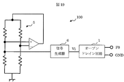
- FIG. 19 is a configuration diagram of a thermal flow meter 100 according to Embodiment 4 of the present invention.
- the thermal flow meter 100 is a sensor that measures the flow rate of air, and includes a measuring element 5, a signal generator 6, and the open drain circuit 1 according to any one of the first to third embodiments.
- the measurement element 5 measures the air flow rate and outputs a measurement voltage Vm corresponding to the measurement result.
- the signal generator 6 generates a periodic signal in which the measurement result represented by the measurement voltage Vm is expressed by the frequency, and outputs this as an input signal Vi to the open drain circuit 1. Since the thermal flow meter 100 represents the air flow rate by the frequency of the periodic signal, it is preferable to use the open drain circuit 1 according to the first to third embodiments.
- the present invention is not limited to the above-described embodiment, and includes various modifications.
- the above embodiment has been described in detail for easy understanding of the present invention, and is not necessarily limited to the one having all the configurations described. For example, the following modifications can be considered.
- FET field effect transistor
- a triangular wave is used as the input signal Vi.
- another periodic signal such as a sine wave or a trapezoidal wave is used, the same configuration as that of the present invention can be used.
- the cycle of the input signal Vi and the delay time ⁇ are proportional.
- the input signal Vi is not necessarily limited to the first-order proportional relationship, and any other can be used as long as ⁇ increases or decreases according to the increase or decrease of Vi. It may have the correspondence relationship.
Landscapes
- Physics & Mathematics (AREA)
- Engineering & Computer Science (AREA)
- Computer Hardware Design (AREA)
- Fluid Mechanics (AREA)
- General Physics & Mathematics (AREA)
- Computing Systems (AREA)
- General Engineering & Computer Science (AREA)
- Mathematical Physics (AREA)
- Electronic Switches (AREA)
- Measuring Volume Flow (AREA)
Abstract
Description
以下では本発明の理解を容易にするため、まず初めに従来技術の課題についてその詳細を説明し、その後に本発明の実施形態について説明する。
V=A*(1-Exp(-β*t))+α ・・・式2


。出力信号の周期はパルス信号と同じT1である。
。したがって、オープンドレイントランジスタTr1~Tr3が全て同じ動作状態(導通または非導通)になることがないので、信号波形が上限(Hiレベル)と下限(Lowレベル)に到達することができない。すなわち、出力信号の波高値が小さくなり、周期はT3より短く、一定周期でなくなる。
図7は、本発明の実施形態1に係るオープンドレイン回路1の回路図である。図7において、3個のオープンドレイントランジスタTr1~Tr3がそれぞれ電流制限抵抗Rd1~Rd3を介して出力端子Foに接続されている。入力端子Viには、トランジスタTr1~Tr3駆動する入力信号Viが入力される。
Vg2=Vi*(Rg3+Rg4)/(Rg1+Rg2+Rg3+Rg4) ・・・式7
Vg3=Vi*Rg4/(Rg1+Rg2+Rg3+Rg4) ・・・式8
Vi=Vth*(Rg1+Rg2+Rg3+Rg4)/(Rg3+Rg4) ・・・式10
Vi=Vth*(Rg1+Rg2+Rg3+Rg4)/Rg4 ・・・式11
Vfo1=Vp*Rd1/(Rd1+Rp) ・・・式13
Vfo2=Vp*Rd12/(Rd12+Rp) ・・・式14
Vfo3=Vp*Rd123/(Rd123+Rp) ・・・式15
Rd123=Rd1*Rd2*Rd3/(Rd1*Rd2+Rd2*Rd3+Rd3*Rd1) ・・・式17
T1/T2=τ1/τ2 ・・・式18
以上のように、本実施形態1に係るオープンドレイン回路1は、各トランジスタTr1~Tr3を切り替えるタイミングをトランジスタ毎にずらす遅延回路(本実施形態1においては分圧回路)を備える。遅延回路は、オープンドレイン回路1に対する入力信号Viの周波数に応じて、各トランジスタ間の遅延時間間隔τを変化させる。したがって、入力信号Viの周期が短くなると遅延時間間隔τもこれにともなって短くなるので、図6に示したような出力信号の波形異常を抑制することができる。すなわち、入力信号Viの周波数によって情報を表し、周波数測定回路2がその周波数を測定することによりその情報を取得する場合において、図6のような測定異常を抑制することができる。
実施形態1で説明した式13~式15に示すように、出力電圧Vfoが階段状に切り替わる際の電圧Vfo1~Vfo3はプルアップ電源Vpをプルアップ抵抗Rpと電流制限抵抗Rd1~Rd3によって分圧したものである。プルアップ抵抗Rpや電流制限抵抗Rd1~Rd3は半導体プロセスによって製造される場合が多い。半導体プロセスによって製造される抵抗体は抵抗値のばらつきがあり、例えば±20%ほどに達する場合がある。また、抵抗値の温度特性もばらつきがある。オープンドレイン回路1と周波数測定回路2はそれぞれ別々に製造されるため、プルアップ抵抗Rpと電流制限抵抗Rd1~Rd3は抵抗値の比も抵抗値温度特性の比も製品ごとにばらつくことが多い。このような抵抗値ばらつきがあると実製品において次のような問題が発生する。
以上のように、本実施形態2に係るオープンドレイン回路1は、プルアップ抵抗Rpと電流制限抵抗Rd1~Rd3の抵抗値ばらつきによって生じる図12のような課題を抑制することができる。さらに、従来のオープンドレイン回路において同様の構成を採用した場合における図15のような急峻な出力変化も抑制することができる。
図16は、本発明の実施形態3に係るオープンドレイン回路1の出力信号波形を示す図である。図16において、各オープンドレイントランジスタ間の切り替え時期の時間差τが複数設定されている。Tr1とTr2との間の時間差はτ1であり、Tr2とTr3との間の時間差はτ2である。τ1とτ2は式9~式11にしたがって定まるので、分圧抵抗Rg1~Rg4による分圧比を調整することにより、τ1とτ2を図16のように調整することができる。
)よりも小さい。一方で出力電圧Vfoが低電位から高電位へ切り替わるときは、先に切り替わるスイッチング素子の遅延時間間隔(τ2)の方が後に切り替わるスイッチング素子の遅延時間間隔(τ1)よりも小さい。すなわち、時刻によってτ1やτ2が変化している。
図19は、本発明の実施形態4に係る熱式流量計100の構成図である。熱式流量計100は、空気の流量を測定するセンサであり、計測素子5、信号生成器6、実施形態1~3いずれかのオープンドレイン回路1を備える。計測素子5は空気の流量を測定し、測定結果に対応する計測電圧Vmを出力する。信号生成器6は、計測電圧Vmが表す計測結果を周波数によって表現した周期信号を生成し、これを入力信号Viとしてオープンドレイン回路1に出力する。熱式流量計100は、周期信号の周波数によって空気の流量を表しているので、実施形態1~3に係るオープンドレイン回路1を用いるのが好適である。
Claims (10)
- 空気の流量を周波数によって表す出力信号を出力する熱式流量計であって、
前記流量を周波数によって表す周期信号を生成する信号生成器、
並列接続された複数のスイッチング素子によって構成され、前記周期信号に対応する前記出力信号を出力する分流回路、
各前記スイッチング素子がそれぞれ前記周期信号の異なる位相においてONになるように、各前記スイッチング素子の動作タイミングを前記スイッチング素子毎に遅延させる遅延回路、
を備え、
前記分流回路は、各前記スイッチング素子がONになる毎に前記出力信号の信号レベルをHighレベルから段階的に下げ、全ての前記スイッチング素子がONになると前記出力信号の信号レベルをLowレベルまで低下させるように構成されており、
前記遅延回路は、前記周期信号の周波数が高くなるにつれて前記遅延の時間幅を短く変化させ、前記周期信号の周波数が低くなるにつれて前記遅延の時間幅を長く変化させる
ことを特徴とする熱式流量計。 - 前記遅延回路は、前記周期信号の周波数に比例して、前記遅延の時間幅を変化させる
ことを特徴とする請求項1記載の熱式流量計。 - 前記スイッチング素子のうち少なくともいずれかは、前記出力信号を出力する側の端子に接続された電流制限抵抗を備える
ことを特徴とする請求項1記載の熱式流量計。 - 前記分流回路の最終段に配置されている前記スイッチング素子は前記電流制限抵抗を備えておらず、前記分流回路のその他の前記スイッチング素子は前記電流制限抵抗を備えている
ことを特徴とする請求項3記載の熱式流量計。 - 前記遅延回路は、前記分流回路が備える各前記スイッチング素子をON状態からOFF状態へ切り替える順番と、OFF状態からON状態へ切り替える順番とが互いに反対になるように、各前記スイッチング素子の動作タイミングを調整する
ことを特徴とする請求項1記載の熱式流量計。 - 前記分流回路の最終段に配置されている前記スイッチング素子は前記電流制限抵抗を備えておらず、前記分流回路のその他の前記スイッチング素子は前記電流制限抵抗を備えており、
前記遅延回路は、前記分流回路が備える各前記スイッチング素子をON状態からOFF状態へ切り替える順番と、OFF状態からON状態へ切り替える順番とが互いに反対になるように、各前記スイッチング素子の動作タイミングを調整し、
前記遅延回路は、前記出力信号がHighレベルからLowレベルに切り替わるときは前記電流制限抵抗を備えていない前記スイッチング素子を最後にON状態とし、前記出力信号がLowレベルからHighレベルに切り替わるときは前記電流制限抵抗を備えていない前記スイッチング素子を最初にOFF状態とする
ことを特徴とする請求項3記載の熱式流量計。 - 前記遅延回路は、各前記スイッチング素子のゲート端子に印加される電圧を前記スイッチング素子毎にそれぞれ異なる値へ分圧する分圧回路を用いて構成されている
ことを特徴とする請求項1記載の熱式流量計。 - 前記遅延回路は、前記周期信号の周期に応じて前記遅延の時間幅を計算しその時間幅にしたがって前記スイッチング素子を駆動する演算回路を用いて構成されている
ことを特徴とする請求項1記載の熱式流量計。 - 前記遅延回路は、いずれかの前記スイッチング素子間の前記遅延の時間幅が、他の前記スイッチング素子間の前記遅延の時間幅とは異なるように、前記遅延の時間幅を調整する
ことを特徴とする請求項1記載の熱式流量計。 - 前記信号生成器は、前記周期信号として三角波信号を生成する
ことを特徴とする請求項1記載の熱式流量計。
Priority Applications (4)
| Application Number | Priority Date | Filing Date | Title |
|---|---|---|---|
| JP2016523478A JP6185168B2 (ja) | 2014-05-30 | 2015-05-25 | 熱式流量計 |
| EP15798963.3A EP3150977B1 (en) | 2014-05-30 | 2015-05-25 | Thermal-type flow meter |
| US15/311,206 US9958306B2 (en) | 2014-05-30 | 2015-05-25 | Thermal type flow meter |
| CN201580028619.6A CN106461441B (zh) | 2014-05-30 | 2015-05-25 | 热式流量计 |
Applications Claiming Priority (2)
| Application Number | Priority Date | Filing Date | Title |
|---|---|---|---|
| JP2014112979 | 2014-05-30 | ||
| JP2014-112979 | 2014-05-30 |
Publications (1)
| Publication Number | Publication Date |
|---|---|
| WO2015182531A1 true WO2015182531A1 (ja) | 2015-12-03 |
Family
ID=54698862
Family Applications (1)
| Application Number | Title | Priority Date | Filing Date |
|---|---|---|---|
| PCT/JP2015/064844 Ceased WO2015182531A1 (ja) | 2014-05-30 | 2015-05-25 | 熱式流量計 |
Country Status (5)
| Country | Link |
|---|---|
| US (1) | US9958306B2 (ja) |
| EP (1) | EP3150977B1 (ja) |
| JP (1) | JP6185168B2 (ja) |
| CN (1) | CN106461441B (ja) |
| WO (1) | WO2015182531A1 (ja) |
Cited By (1)
| Publication number | Priority date | Publication date | Assignee | Title |
|---|---|---|---|---|
| JPWO2019239726A1 (ja) * | 2018-06-13 | 2021-05-13 | 日立Astemo株式会社 | 物理量検出装置 |
Families Citing this family (1)
| Publication number | Priority date | Publication date | Assignee | Title |
|---|---|---|---|---|
| CN109470325B (zh) * | 2018-09-20 | 2021-03-16 | 北京七星华创流量计有限公司 | 气体流量测量方法、装置以及控制系统和气体质量流量计 |
Citations (7)
| Publication number | Priority date | Publication date | Assignee | Title |
|---|---|---|---|---|
| JPS6435218A (en) * | 1987-07-30 | 1989-02-06 | Hitachi Ltd | Hot wire type air flowmeter |
| JPH08228141A (ja) * | 1995-02-21 | 1996-09-03 | Kawasaki Steel Corp | 出力バッファ回路 |
| JPH11239046A (ja) * | 1998-02-23 | 1999-08-31 | Nec Corp | トランジスタ駆動装置及びその駆動方法 |
| JP2001285051A (ja) * | 2000-03-29 | 2001-10-12 | Kawasaki Steel Corp | 出力バッファ回路 |
| JP2005311664A (ja) * | 2004-04-21 | 2005-11-04 | Hitachi Ltd | 周波数出力回路 |
| JP2005333618A (ja) * | 2004-04-22 | 2005-12-02 | Nec Electronics Corp | 出力バッファ回路 |
| JP2010010767A (ja) * | 2008-06-24 | 2010-01-14 | Hitachi Ltd | 周波数出力装置、流量計、及び流量計測装置 |
Family Cites Families (9)
| Publication number | Priority date | Publication date | Assignee | Title |
|---|---|---|---|---|
| US4043196A (en) * | 1976-02-09 | 1977-08-23 | Technology Incorporated | Method and apparatus for effecting fluid flow measurement in a single sensor |
| JPH01228214A (ja) | 1988-03-08 | 1989-09-12 | Matsushita Electron Corp | 半導体集積回路 |
| JP3463757B2 (ja) | 1993-04-08 | 2003-11-05 | 株式会社日立製作所 | エンジン制御装置及びこれに用いる空気流量計 |
| JPH0897701A (ja) * | 1994-09-21 | 1996-04-12 | Mitsubishi Electric Corp | 半導体回路 |
| JP3808038B2 (ja) * | 2003-01-14 | 2006-08-09 | 株式会社日立製作所 | 周波数出力型熱線式流量計 |
| US8115540B2 (en) * | 2006-09-14 | 2012-02-14 | Nec Corporation | Amplifying apparatus, method of output control and control program |
| JP5999592B2 (ja) * | 2011-09-07 | 2016-09-28 | ローム株式会社 | 受信回路、半導体装置、センサ装置 |
| US9631965B2 (en) * | 2012-02-15 | 2017-04-25 | Sensortechnics GmbH | Offset compensation for flow sensing devices |
| CN103837243B (zh) * | 2014-03-27 | 2016-08-24 | 卓捷创芯科技(深圳)有限公司 | 时间域集成温度传感器 |
-
2015
- 2015-05-25 CN CN201580028619.6A patent/CN106461441B/zh not_active Expired - Fee Related
- 2015-05-25 EP EP15798963.3A patent/EP3150977B1/en not_active Not-in-force
- 2015-05-25 WO PCT/JP2015/064844 patent/WO2015182531A1/ja not_active Ceased
- 2015-05-25 US US15/311,206 patent/US9958306B2/en active Active
- 2015-05-25 JP JP2016523478A patent/JP6185168B2/ja not_active Expired - Fee Related
Patent Citations (7)
| Publication number | Priority date | Publication date | Assignee | Title |
|---|---|---|---|---|
| JPS6435218A (en) * | 1987-07-30 | 1989-02-06 | Hitachi Ltd | Hot wire type air flowmeter |
| JPH08228141A (ja) * | 1995-02-21 | 1996-09-03 | Kawasaki Steel Corp | 出力バッファ回路 |
| JPH11239046A (ja) * | 1998-02-23 | 1999-08-31 | Nec Corp | トランジスタ駆動装置及びその駆動方法 |
| JP2001285051A (ja) * | 2000-03-29 | 2001-10-12 | Kawasaki Steel Corp | 出力バッファ回路 |
| JP2005311664A (ja) * | 2004-04-21 | 2005-11-04 | Hitachi Ltd | 周波数出力回路 |
| JP2005333618A (ja) * | 2004-04-22 | 2005-12-02 | Nec Electronics Corp | 出力バッファ回路 |
| JP2010010767A (ja) * | 2008-06-24 | 2010-01-14 | Hitachi Ltd | 周波数出力装置、流量計、及び流量計測装置 |
Non-Patent Citations (1)
| Title |
|---|
| See also references of EP3150977A4 * |
Cited By (1)
| Publication number | Priority date | Publication date | Assignee | Title |
|---|---|---|---|---|
| JPWO2019239726A1 (ja) * | 2018-06-13 | 2021-05-13 | 日立Astemo株式会社 | 物理量検出装置 |
Also Published As
| Publication number | Publication date |
|---|---|
| CN106461441B (zh) | 2019-09-06 |
| JPWO2015182531A1 (ja) | 2017-04-20 |
| JP6185168B2 (ja) | 2017-08-23 |
| CN106461441A (zh) | 2017-02-22 |
| US20170082472A1 (en) | 2017-03-23 |
| EP3150977A4 (en) | 2018-02-14 |
| US9958306B2 (en) | 2018-05-01 |
| EP3150977B1 (en) | 2020-12-16 |
| EP3150977A1 (en) | 2017-04-05 |
Similar Documents
| Publication | Publication Date | Title |
|---|---|---|
| JP6498473B2 (ja) | スイッチ駆動回路 | |
| CN103944550B (zh) | 用于驱动负载的方法 | |
| JP5287916B2 (ja) | 負荷駆動装置 | |
| US10164629B2 (en) | Method and apparatus for controlling current slew rate of a switching current through an external resistive load | |
| JP2005192394A5 (ja) | ||
| JP2006191677A (ja) | スイッチング回路をプッシュ−プルする不感時間の適宜な制御 | |
| CN103856043A (zh) | 控制电路和四开关升降压型变换器 | |
| JP6355775B2 (ja) | ゲートドライバ、及びスイッチング方法 | |
| CN107314830A (zh) | 用于修正温度测量信号的设备 | |
| JP6354129B2 (ja) | センサ信号出力回路およびセンサ信号出力回路の調整方法 | |
| CN105278603B (zh) | 栅极电位控制电路 | |
| JP6185168B2 (ja) | 熱式流量計 | |
| JP6319126B2 (ja) | 温度補正回路および感温素子の検出温度補正方法 | |
| DK201570208A1 (en) | Zero drift, limitless and adjustable reference voltage generation | |
| JP6366436B2 (ja) | 電圧制御装置 | |
| CN103812340A (zh) | 开关调节器 | |
| CN106787902A (zh) | 一种修正波逆变器输出电压控制系统及控制方法 | |
| US6552579B1 (en) | Fuel gauge power switch with current sense | |
| TW201504604A (zh) | 功率元件溫度監視器 | |
| EP2704520A1 (en) | An induction heating generator and an induction cooking hob | |
| TW200824243A (en) | Switching regulator | |
| US9883611B2 (en) | Fan control circuit | |
| TWI463144B (zh) | 可偵測突波訊號特性之突波偵測裝置 | |
| JP6642074B2 (ja) | スイッチング素子の駆動装置 | |
| TW201310040A (zh) | 功率測試系統 |
Legal Events
| Date | Code | Title | Description |
|---|---|---|---|
| 121 | Ep: the epo has been informed by wipo that ep was designated in this application |
Ref document number: 15798963 Country of ref document: EP Kind code of ref document: A1 |
|
| ENP | Entry into the national phase |
Ref document number: 2016523478 Country of ref document: JP Kind code of ref document: A |
|
| WWE | Wipo information: entry into national phase |
Ref document number: 15311206 Country of ref document: US |
|
| REEP | Request for entry into the european phase |
Ref document number: 2015798963 Country of ref document: EP |
|
| WWE | Wipo information: entry into national phase |
Ref document number: 2015798963 Country of ref document: EP |
|
| NENP | Non-entry into the national phase |
Ref country code: DE |