WO2015194361A1 - 放射線検出器及びその製造方法 - Google Patents
放射線検出器及びその製造方法 Download PDFInfo
- Publication number
- WO2015194361A1 WO2015194361A1 PCT/JP2015/065879 JP2015065879W WO2015194361A1 WO 2015194361 A1 WO2015194361 A1 WO 2015194361A1 JP 2015065879 W JP2015065879 W JP 2015065879W WO 2015194361 A1 WO2015194361 A1 WO 2015194361A1
- Authority
- WO
- WIPO (PCT)
- Prior art keywords
- filling portion
- moisture
- scintillator layer
- radiation detector
- filling
- Prior art date
- Legal status (The legal status is an assumption and is not a legal conclusion. Google has not performed a legal analysis and makes no representation as to the accuracy of the status listed.)
- Ceased
Links
Images



Classifications
-
- G—PHYSICS
- G01—MEASURING; TESTING
- G01T—MEASUREMENT OF NUCLEAR OR X-RADIATION
- G01T1/00—Measuring X-radiation, gamma radiation, corpuscular radiation, or cosmic radiation
- G01T1/16—Measuring radiation intensity
- G01T1/20—Measuring radiation intensity with scintillation detectors
- G01T1/2002—Optical details, e.g. reflecting or diffusing layers
-
- G—PHYSICS
- G01—MEASURING; TESTING
- G01T—MEASUREMENT OF NUCLEAR OR X-RADIATION
- G01T1/00—Measuring X-radiation, gamma radiation, corpuscular radiation, or cosmic radiation
- G01T1/16—Measuring radiation intensity
- G01T1/20—Measuring radiation intensity with scintillation detectors
- G01T1/2018—Scintillation-photodiode combinations
- G01T1/20188—Auxiliary details, e.g. casings or cooling
- G01T1/20189—Damping or insulation against damage, e.g. caused by heat or pressure
-
- G—PHYSICS
- G01—MEASURING; TESTING
- G01T—MEASUREMENT OF NUCLEAR OR X-RADIATION
- G01T1/00—Measuring X-radiation, gamma radiation, corpuscular radiation, or cosmic radiation
- G01T1/16—Measuring radiation intensity
- G01T1/20—Measuring radiation intensity with scintillation detectors
- G01T1/2006—Measuring radiation intensity with scintillation detectors using a combination of a scintillator and photodetector which measures the means radiation intensity
-
- G—PHYSICS
- G01—MEASURING; TESTING
- G01T—MEASUREMENT OF NUCLEAR OR X-RADIATION
- G01T1/00—Measuring X-radiation, gamma radiation, corpuscular radiation, or cosmic radiation
- G01T1/16—Measuring radiation intensity
- G01T1/20—Measuring radiation intensity with scintillation detectors
- G01T1/202—Measuring radiation intensity with scintillation detectors the detector being a crystal
Definitions
- Embodiments of the present invention relate to a radiation detector and a method of manufacturing the same.
- An example of a radiation detector is an X-ray detector.
- X-rays are converted to visible light, that is, fluorescence by a scintillator layer, and this fluorescence is signaled using a photoelectric conversion element such as an amorphous silicon (a-Si) photodiode or a CCD (Charge Coupled Device).
- a-Si amorphous silicon
- CCD Charge Coupled Device
- An X-ray image is acquired by converting it into electric charge.
- a reflective layer may be further provided on the scintillator layer in order to enhance the utilization efficiency of fluorescence and improve the sensitivity characteristic.
- the scintillator layer and the reflective layer need to be isolated from the external atmosphere.
- the scintillator layer is made of CsI (cesium iodide): Tl (thallium), CsI: Na (sodium) or the like
- CsI calcium iodide
- Na sodium
- the resolution characteristic deterioration due to humidity or the like becomes large. Therefore, as a structure capable of obtaining high moisture-proof performance, a structure in which a scintillator layer and a reflective layer are covered with a hat-shaped moisture-proof body, and a flange of a moisture-proof body is adhered to a substrate has been proposed.
- the scintillator layer and the reflective layer are covered with a hat-shaped moisture-proof body and the flange portion of the moisture-proof body is bonded to the substrate, high moisture-proof performance can be obtained.
- the width dimension of the rim portion of the moisture-proof body is increased, an extra space corresponding to the width dimension is required.
- the wiring pad electrically connected to the flexible printed circuit board or the like needs to be provided further outside the area of the protruding adhesive. Therefore, if the width dimension of the rim of the moisture-proof body is lengthened to secure the area where the adhesive protrudes, the size of the area which needs to be provided around the effective pixel area increases, and thus the size of the radiation detector And increase in weight.
- a structure has been proposed in which a surrounding ring surrounding the scintillator layer is provided and the cover is adhered to the upper surface of the surrounding ring.
- the width dimension of the surrounding ring is increased, the dimension of the area that needs to be provided around the effective pixel area increases, which may result in an increase in the size and weight of the radiation detector.
- the problem to be solved by the present invention is to provide a radiation detector that can achieve space saving and improvement of the moisture proof performance, and a method of manufacturing the same.
- the radiation detector according to the embodiment is provided on an array substrate having a substrate and a plurality of photoelectric conversion devices provided on one surface side of the substrate, and the plurality of photoelectric conversion devices, and the radiation is detected.
- a scintillator layer for converting into fluorescence a wall provided on one surface side of the substrate and surrounding the scintillator layer, a filling portion provided between the scintillator layer and the wall, and the scintillator layer And a moisture-proof body joined to the upper surface of the filling portion in the vicinity of the peripheral portion.
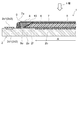
- FIG. 1 is a schematic perspective view for illustrating the X-ray detector 1 according to the first embodiment.
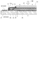
- FIG. 2 is a schematic cross-sectional view of the X-ray detector 1; It is a schematic cross section of the X-ray detector 1a provided with the moisture-proof body 17 which concerns on other embodiment.
- (A) is a schematic front view of the moistureproof body 17.
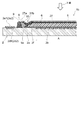
- (B) is a schematic side view of the moistureproof body 17. It is a schematic cross section of the X-ray detector 1b provided with the moisture-proof body 27 which concerns on other embodiment.
- FIG. 5 is a graph for illustrating changes in moisture permeability under a high temperature and high humidity environment (60 ° C.-90% RH).
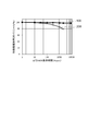
- FIG. 6 is a graph for illustrating changes in resolution characteristics under a high temperature and high humidity environment (60 ° C.-90% RH).
- the radiation detector according to the embodiment of the present invention can be applied to various types of radiation such as ⁇ -rays in addition to X-rays.
- ⁇ -rays in addition to X-rays.
- other radiation can also be applied by replacing “X-ray” in the following embodiments with “other radiation”.
- FIG. 1 is a schematic perspective view for illustrating the X-ray detector 1 according to the first embodiment.
- the reflection layer 6, the moisture proof body 7, the filling part 8, the wall 9, the joining layer 10, etc. are omitted and drawn.
- FIG. 2 is a schematic cross-sectional view of the X-ray detector 1.
- the control line (or gate line) 2 c 1 the data line (or signal line) 2 c 2, the signal processing unit 3, the image transmission unit 4 and the like are omitted to avoid complication. .
- the X-ray detector 1 which is a radiation detector is an X-ray flat sensor which detects an X-ray image which is a radiation image.
- the X-ray detector 1 can be used, for example, in general medical applications. However, the application of the X-ray detector 1 is not limited to the general medical application.
- the X-ray detector 1 includes an array substrate 2, a signal processing unit 3, an image transmission unit 4, a scintillator layer 5, a reflection layer 6, a moistureproof body 7, a filling unit 8 and a wall 9 and a bonding layer 10 are provided.
- the array substrate 2 includes a substrate 2a, a photoelectric conversion unit 2b, a control line 2c1, a data line 2c2, and a protective layer 2f.
- the substrate 2a has a plate-like shape and is formed of a translucent material such as non-alkali glass.
- a plurality of photoelectric conversion units 2b are provided on one surface of the substrate 2a.
- the photoelectric conversion unit 2b has a rectangular shape, and is provided in an area defined by the control line 2c1 and the data line 2c2.
- the plurality of photoelectric conversion units 2b are arranged in a matrix.
- One photoelectric conversion unit 2 b corresponds to one pixel.
- Each of the plurality of photoelectric conversion units 2b is provided with a photoelectric conversion element 2b1 and a thin film transistor (TFT; Thin Film Transistor) 2b2 which is a switching element.
- a storage capacitor (not shown) can be provided to store the signal charge converted in the photoelectric conversion element 2b1.
- the storage capacitors (not shown) have, for example, a rectangular plate shape and can be provided under each thin film transistor 2b2. However, depending on the capacitance of the photoelectric conversion element 2b1, the photoelectric conversion element 2b1 can also serve as a storage capacitor (not shown).
- the photoelectric conversion element 2b1 can be, for example, a photodiode.
- the thin film transistor 2b2 performs switching of accumulation and release of the charge generated when the fluorescence is incident on the photoelectric conversion element 2b1.
- the thin film transistor 2b2 can include a semiconductor material such as amorphous silicon (a-Si) or polysilicon (P-Si).
- the thin film transistor 2b2 has a gate electrode, a source electrode, and a drain electrode.
- the gate electrode of the thin film transistor 2b2 is electrically connected to the corresponding control line 2c1.
- the source electrode of the thin film transistor 2b2 is electrically connected to the corresponding data line 2c2.
- the drain electrode of the thin film transistor 2b2 is electrically connected to the corresponding photoelectric conversion element 2b1 and a storage capacitor (not shown).
- a plurality of control lines 2c1 are provided in parallel with each other at predetermined intervals.
- the control line 2c1 extends in a first direction (for example, the row direction).
- the plurality of control lines 2c1 are electrically connected to the plurality of wiring pads 2d1 provided in the vicinity of the periphery of the substrate 2a.
- One ends of a plurality of wirings provided on the flexible printed board 2e1 are electrically connected to the plurality of wiring pads 2d1, respectively.
- the other ends of the plurality of wires provided on the flexible printed circuit 2e1 are electrically connected to a control circuit (not shown) provided on the signal processing unit 3 respectively.
- a plurality of data lines 2c2 are provided in parallel with each other at predetermined intervals.
- the data line 2c2 extends in a second direction (for example, the column direction) orthogonal to the first direction.
- the plurality of data lines 2c2 are electrically connected to the plurality of wiring pads 2d2 provided in the vicinity of the periphery of the substrate 2a.
- One ends of a plurality of wirings provided on the flexible printed board 2e2 are electrically connected to the plurality of wiring pads 2d2, respectively.
- the other ends of the plurality of wires provided on the flexible printed circuit 2e2 are electrically connected to amplification and conversion circuits (not shown) provided on the signal processing unit 3 respectively.
- the protective layer 2 f is provided to cover the photoelectric conversion unit 2 b, the control line 2 c 1, and the data line 2 c 2.
- the protective layer 2 f can be formed of an insulating material such as silicon nitride (SiN) or an acrylic resin.
- the signal processing unit 3 is provided on the side of the substrate 2a opposite to the side on which the photoelectric conversion unit 2b is provided.
- the signal processing unit 3 is provided with a control circuit (not shown) and an amplification / conversion circuit (not shown).
- a control circuit (not shown) controls the operation of each thin film transistor 2b2, that is, the on state and the off state. For example, a control circuit (not shown) sequentially applies a control signal S1 to each control line 2c1 via the flexible printed circuit 2e1, the wiring pad 2d1 and the control line 2c1.
- the thin film transistor 2b2 is turned on by the control signal S1 applied to the control line 2c1, and the image data signal S2 from the photoelectric conversion unit 2b can be received.
- the amplification / conversion circuit includes, for example, a plurality of charge amplifiers, a parallel-to-serial converter, and an analog-to-digital converter.
- the plurality of charge amplifiers are electrically connected to the respective data lines 2c2.
- the plurality of parallel / serial converters are electrically connected to the plurality of charge amplifiers, respectively.
- the plurality of analog-to-digital converters are electrically connected to the plurality of parallel / serial converters, respectively.
- a plurality of charge amplifiers (not shown) sequentially receive the image data signal S2 from each photoelectric conversion unit 2b through the data line 2c2, the wiring pad 2d2 and the flexible printed board 2e2.
- a plurality of charge amplifiers sequentially amplify the received image data signal S2.
- a plurality of parallel / serial converters sequentially convert the amplified image data signal S2 into a serial signal.
- the plurality of analog-to-digital converters sequentially convert the image data signal S2 converted into the serial signal into a digital signal.
- the image transmission unit 4 is electrically connected to an amplification / conversion circuit (not shown) of the signal processing unit 3 through the wiring 4 a.
- the image transmission unit 4 may be integrated with the signal processing unit 3.
- the image transmission unit 4 constructs an X-ray image based on the image data signal S2 converted into digital signals by a plurality of analog-digital converters (not shown).
- the data of the configured X-ray image is output from the image transmission unit 4 to an external device.
- the scintillator layer 5 is provided on the plurality of photoelectric conversion elements 2b1 and converts incident X-rays into visible light, that is, fluorescence.
- the scintillator layer 5 can be formed using, for example, cesium iodide (CsI): thallium (Tl), or sodium iodide (NaI): thallium (Tl) or the like.
- the scintillator layer 5 is an aggregate of columnar crystals.
- the scintillator layer 5 composed of a collection of columnar crystals can be formed, for example, using a vacuum evaporation method or the like.
- the thickness dimension of the scintillator layer 5 can be, for example, about 600 ⁇ m.
- the thickness dimension of a pillar of a columnar crystal can be, for example, about 8 ⁇ m to 12 ⁇ m at the outermost surface.
- the scintillator layer 5 can also be formed using, for example, gadolinium oxysulfide (Gd 2 O 2 S) or the like.
- the scintillator layer 5 can be formed as follows. First, particles of gadolinium oxysulfide are mixed with a binder material. Next, the mixed material is applied so as to cover an area provided with the plurality of photoelectric conversion units 2 b on the substrate 2 a. Next, the applied material is fired. Next, a groove is formed in the fired material using a blade dicing method or the like.
- the grooves can be filled with air (air) or an inert gas such as nitrogen gas for oxidation prevention. Also, the groove may be in a vacuum state.
- the reflective layer 6 is provided to enhance the utilization efficiency of fluorescence and improve the sensitivity characteristic. That is, of the fluorescence generated in the scintillator layer 5, the reflective layer 6 reflects light traveling to the opposite side to the side on which the photoelectric conversion unit 2 b is provided, and directs the light to the photoelectric conversion unit 2 b.
- the reflective layer 6 covers the X-ray incident side of the scintillator layer 5.
- the reflective layer 6 can be formed, for example, by applying a resin containing light scattering particles such as titanium oxide (TiO 2 ) on the scintillator layer 5.
- the reflective layer 6 can also be formed, for example, by forming a layer made of a metal having a high light reflectance, such as a silver alloy or aluminum, on the scintillator layer 5.
- the reflective layer 6 can also be formed using, for example, a plate whose surface is made of a metal having a high light reflectance such as a silver alloy or aluminum.
- the reflection layer 6 illustrated in FIG. 2 applies a submicron powder made of titanium oxide, a binder resin, and a material prepared by mixing a solvent on the X ray incident side of the scintillator layer 5, Formed by drying.
- the thickness dimension of the reflective layer 6 can be about 120 ⁇ m.
- the reflective layer 6 is not necessarily required, and may be provided as necessary. Below, the case where the reflection layer 6 is provided is illustrated.
- the moistureproof body 7 is provided to prevent deterioration of the characteristics of the reflective layer 6 and the characteristics of the scintillator layer 5 due to water vapor contained in the air.
- the moistureproof body 7 covers the upper side of the reflective layer 6. In this case, there may be a gap between the moisture-proof body 7 and the upper surface of the reflective layer 6, or the upper surface of the moisture-proof body 7 and the reflective layer 6 may be in contact. For example, when the moisture-proof body 7 and the upper surface of the filling portion 8 are joined in an environment decompressed below atmospheric pressure, the upper surface of the moisture-proof body 7 and the reflective layer 6 contacts with atmospheric pressure.
- the moistureproof body 7 covers the upper side of the scintillator layer 5, and the vicinity of the peripheral portion is joined to the upper surface of the filling portion 8.
- the position of the end face 7 a of the moistureproof body 7 can be outside the effective pixel area A and can be inside the inner surface 9 a of the wall 9 in a plan view. In this case, if the position of the end face 7a of the moistureproof body 7 is close to the inner surface 9a of the wall body 9 in plan view, the sealing performance and reliability between the upper surface of the filling portion 8 and the moistureproof body 7 is improved. It can be done.
- the moistureproof body 7 has a film shape, a foil shape, or a thin plate shape.
- the moistureproof body 7 can be formed of a material having a low moisture permeability coefficient.
- the moistureproof body 7 is formed by laminating, for example, aluminum, an aluminum alloy, or a film made of a resin film and an inorganic material (a metal such as aluminum or aluminum alloy, or a ceramic material such as SiO 2 , SiON, or Al 2 O 3 ). It can be formed from a low moisture-permeable moisture-proof film (water vapor barrier film) or the like. In this case, if the moisture-proof body 7 is formed using aluminum, an aluminum alloy or the like having an effective moisture permeability coefficient almost zero, the water vapor passing through the moisture-proof body 7 can be almost completely eliminated.
- the thickness dimension of the moistureproof body 7 can be determined in consideration of the absorption of X-rays, rigidity, and the like. In this case, if the thickness dimension of the moistureproof body 7 is too large, the absorption of X-rays becomes too large. If the thickness dimension of the moisture-proof body 7 is too small, the rigidity is reduced and it is easily broken.
- the moistureproof body 7 can be formed, for example, using an aluminum foil having a thickness dimension of 0.1 mm.
- the filling portion 8 is provided between the side surface of the scintillator layer 5 covered by the reflective layer 6 and the inner surface 9 a of the wall body 9.
- the position of the upper surface of the filling portion 8 can be made substantially the same as the position of the upper surface of the scintillator layer 5 covered by the reflective layer 6.
- the position of the upper surface of the filling portion 8 may be the same as the position of the upper surface of the scintillator layer 5 covered by the reflective layer 6 or from the position of the upper surface of the scintillator layer 5 covered by the reflective layer 6 It may be slightly higher, or slightly lower than the position of the upper surface of the scintillator layer 5 covered by the reflective layer 6.
- the position of the upper surface of the filling portion 8 can be slightly lower than the position of the upper surface of the wall 9. If the position of the upper surface of the filling portion 8 is slightly lower than the position of the upper surface of the wall 9, the material for forming the filling portion 8 exceeds the upper surface of the wall 9 when performing the filling described later. To avoid spilling out.
- the filling portion 8 includes, for example, a filler material made of an inorganic material and a resin (for example, an epoxy resin).
- the filler material can be made of, for example, talc (talc: Mg 3 Si 4 O 10 (OH) 2 ) or the like.
- Talc is an inorganic material with low hardness and has high slipperiness. Therefore, even if talc is contained at a high concentration, the shape deformation of the filling portion 8 does not become difficult.
- the concentration (packing density) of talc can be increased.
- the moisture permeability coefficient can be lowered by about one digit as compared with the case of using only the resin.
- the reflective layer 6 also contains titanium oxide which is an inorganic material.
- the inorganic material contained in the reflective layer 6 is for improving the light scattering property.
- the light scattering property depends on the type of inorganic material (refractive index, transparency and stability, etc.), particle size (eg, average particle size of about 0.3 ⁇ m is desirable) and ratio of binder resin, type and content of solvent, etc. It can be made appropriate.
- the inorganic material contained in the filling portion 8 is for reducing the moisture permeability. Therefore, if the concentration of the inorganic material is too low, the amount of moisture permeation increases, and the resolution characteristics may be degraded.
- the concentration of the inorganic material contained in the filling portion 8 does not cause a gap with the resin material, cause a crack upon drying after filling, or impair the flowability necessary for forming the filling portion (filling) It is preferable to make it high in the range where it is difficult to form a gap between parts.
- the concentration of the filler material made of talc contained in the filling portion 8 can be 50% by weight or more.
- the upper surface of the filling portion 8 is preferably flat. If the upper surface of the filling portion 8 is flat, the sealing property between the upper surface of the filling portion 8 and the moisture-proof body 7 can be secured, and high reliability can be obtained. In this case, by lowering the viscosity of the material for forming the filling portion 8, the upper surface of the filling portion 8 can be made flat.
- the viscosity of the material for forming the filling portion 8 may be about 120 Pa ⁇ sec or less at room temperature.
- the filling part 8 can also be made to contain a hygroscopic material and resin (for example, epoxy resin etc.).
- the material for forming the filling portion 8 can be prepared by mixing, for example, calcium chloride, which is a hygroscopic material, a binder resin (for example, an epoxy resin or a silicone resin), and a solvent. .
- the density can be about 2.1 g / cc
- the moisture absorption capacity per unit weight can be about 27%
- the viscosity can be about 120 Pa ⁇ sec or less at room temperature.
- an epoxidized vegetable oil such as epoxidized linseed oil can be further added to form a flexible filling portion 8.
- the filling portion 8 having flexibility, due to the flexibility, it is possible to suppress peeling due to stress caused by temperature change and thermal expansion difference between members.
- the wall 9 has a frame shape.
- the wall body 9 is provided outside the scintillator layer 5 in a plan view and inside the region where the wiring pads 2d1 and 2d2 are provided. In this case, if the wall body 9 is provided in the vicinity of the region where the wiring pads 2d1 and 2d2 are provided, the area of the upper surface of the filling portion 8 can be increased. Therefore, the sealing property and reliability between the upper surface of the filling portion 8 and the moisture-proof body 7 can be improved.
- the material for forming the wall 9 can have a low moisture permeability coefficient.
- the wall body 9 contains, for example, a filler material made of an inorganic material and a resin (for example, an epoxy resin).
- the material for forming the wall 9 may be the same as the material for forming the filling portion 8.
- the viscosity of the material for forming the wall 9 is higher than the viscosity of the material for forming the filling portion 8.
- the viscosity of the material for forming the wall body 9 can be, for example, about 340 Pa ⁇ sec at room temperature.
- the wall body 9 can also be formed of, for example, a metal such as aluminum or an inorganic material such as glass.
- the frame 9 is formed first, and then the material of the filling portion 8 is filled in the gap between the frame 9 and the side surface of the scintillator layer 5 and the reflective layer 6 and hardened. And the filling portion 8 can be formed.
- the bonding layer 10 is provided between the moisture-proof body 7 and the upper surface of the filling portion 8, and bonds the vicinity of the periphery of the moisture-proof body 7 and the filling portion 8.
- the bonding layer 10 need not be limited to the upper portion of the filling portion 8.
- the bonding layer 10 may be extended to the upper portion of the outer wall 9 of the filling portion 8 or the peripheral upper portion of the reflective layer 6 or the scintillator layer 5 inside the filling portion 8 without any problem.
- the bonding layer 10 is, for example, a delayed curing adhesive (a UV curing adhesive of a type in which the curing reaction becomes apparent after a certain time after UV irradiation), a natural (normal temperature) curing adhesive, and a heat curing type. It can be formed by curing any of the adhesives.
- FIG. 3 is a schematic cross-sectional view of an X-ray detector 1a provided with a moistureproof body 17 according to another embodiment.
- FIG. 4A is a schematic front view of the moistureproof body 17.
- FIG. 4 (b) is a schematic side view of the moistureproof body 17.
- the X-ray detector 1 a includes the array substrate 2, the signal processing unit 3, the image transmission unit 4, the scintillator layer 5, the reflection layer 6, the moistureproof body 17, the filling unit 8, the wall 9, and The bonding layer 10 is provided.
- the moisture-proof body 17 has a hat shape, and has a surface portion 17b, a circumferential surface portion 17c, and a brim portion 17d.
- the moistureproof body 17 can be one in which the surface portion 17b, the circumferential surface portion 17c, and the flange portion 17d are integrally formed.
- the material of the moistureproof body 17 can be the same as the material of the moistureproof body 7 described above.
- the thickness of the moistureproof body 17 can be the same as the thickness of the moistureproof body 7 described above.
- the surface portion 17 b faces the surface side (the X-ray incident surface side) of the scintillator layer 5.
- the circumferential surface portion 17c is provided to surround the periphery of the surface portion 17b.
- the circumferential surface portion 17c extends from the peripheral edge of the surface portion 17b toward the substrate 2a. There may be a gap between the surface portion 17 b and the reflective layer 6.
- the flange portion 17 d is provided so as to surround an end of the circumferential surface portion 17 c opposite to the surface portion 17 b.
- the flange 17 d extends outward from the end of the circumferential surface 17 c.
- the flange portion 17d has a ring shape.
- the flange portion 17 d is bonded to the upper surface of the filling portion 8 via the bonding layer 10.
- the position of the end face 17a of the moistureproof body 17 is outside the effective pixel area A in plan view, and is outside the inner face 9a of the wall 9 or the same as the inner face 9a or inside the inner face 9a. Can be In this case, if the position of the end face 17a of the moistureproof body 17 in the planar view is made closer to the outside than the inner surface 9a of the wall 9 or to the inner side of the inner surface 9a, Sealability and reliability of the upper surface and the moistureproof body 17 (collar portion 17d) can be improved.
- the hat-shaped moisture-proof body 17 can enhance the rigidity. Moreover, when bonding the moisture-proof body 17 to the upper surface of the filling part 8, it can position using the solid
- FIG. 5 is a schematic cross-sectional view of an X-ray detector 1b provided with a moistureproof body 27 according to another embodiment.
- the X-ray detector 1 b includes the array substrate 2, the signal processing unit 3, the image transmission unit 4, the scintillator layer 5, the reflective layer 6, the moistureproof body 27, the filling unit 8, the wall 9, and The bonding layer 10 is provided. That is, the X-ray detector 1 b is provided with a moisture-proof body 27 instead of the moisture-proof body 7 described above.
- a bent portion 27b protruding toward the substrate 2a side is provided in the vicinity of the peripheral edge of the moistureproof body 27 in the vicinity of the peripheral edge of the moistureproof body 27.
- the bending portion 27 b is provided to surround the periphery of the moisture-proof body 27.
- the bent portion 27 b is bonded to the upper surface of the filling portion 8 via the bonding layer 10.
- the position of the end face 27a of the moistureproof body 27 is outside the effective pixel area A in plan view, and is outside the inner face 9a of the wall 9 or the same as the inner face 9a or inside the inner face 9a.
- the rigidity can be enhanced.
- the positioning can also be performed by fitting the bending portion 27 b into the recess provided on the upper surface of the filling portion 8.
- the workability and bonding accuracy when bonding the moisture-proof body 27 to the upper surface of the filling portion 8 can be improved. Further, by providing the bent portion 27b, the bonding area can be increased. Therefore, the bonding strength can be improved and the moisture proof performance can be improved.
- FIG. 6 is a graph for illustrating changes in moisture permeability under a high temperature and high humidity environment (60 ° C.-90% RH).
- 200 in FIG. 6 is a case where the moisture-proof body 7 is joined to the upper surface of the wall body 9 and the filling portion 8 is not provided.
- Reference numerals 100 and 101 in FIG. 6 denote the case of the X-ray detector 1 according to the present embodiment.
- 100 is a case where the filling part 8 is formed from resin containing a filler material.
- 101 is a case where the filling part 8 is formed from resin containing a hygroscopic material. As can be seen from FIG. 6, if the filling portion 8 is provided, the amount of moisture permeation can be reduced.
- FIG. 7 is a graph for illustrating changes in resolution characteristics under a high temperature and high humidity environment (60 ° C.-90% RH).
- 200 in FIG. 7 is a case where the moisture-proof body 7 is joined to the upper surface of the wall body 9 and the filling portion 8 is not provided.
- Reference numeral 100 in FIG. 7 denotes the case of the X-ray detector 1 according to the present embodiment.
- 100 is a case where the filling part 8 is formed from resin containing a filler material.
- FIG. 7 also shows how the resolution characteristics obtained by the scintillator layer 5 and the reflective layer 6 deteriorate with the passage of storage time in a high temperature and high humidity environment (60.degree. C.-90% RH). .
- the moistureproof bodies 7, 17, 27 can be bonded to the upper surface of the filling portion 8. Therefore, the moistureproof bodies 7, 17, It is not necessary to provide a space for joining 27. Therefore, the X-ray detectors 1, 1a, and 1b can be miniaturized and made lighter. Moreover, if the filling portion 8 is provided, the moisture proof performance can be improved, and it is also possible to suppress the deterioration of the resolution characteristic.
- the array substrate 2 is created.
- the array substrate 2 can be formed, for example, by sequentially forming the photoelectric conversion unit 2b, the control line 2c1, the data line 2c2, the wiring pad 2d1, the wiring pad 2d2, the protective layer 2f, and the like on the substrate 2a.
- the array substrate 2 can be produced, for example, using a semiconductor manufacturing process.
- the scintillator layer 5 is provided so as to cover the region of the array substrate 2 in which the plurality of photoelectric conversion units 2 b are formed.
- the scintillator layer 5 can be formed, for example, by depositing a film of cesium iodide: thallium using a vacuum evaporation method or the like.
- the thickness dimension of the scintillator layer 5 can be approximately 600 ⁇ m.
- the thickness dimension of the pillars of the columnar crystals can be about 8 to 12 ⁇ m at the outermost surface.
- the reflective layer 6 is formed so as to cover the surface of the scintillator layer 5 (the X-ray incident surface side).
- the reflective layer 6 can be formed, for example, by applying a material prepared by mixing a submicron powder of titanium oxide, a binder resin, and a solvent on the scintillator layer 5 and drying it.
- the scintillator layer 5 covered by the reflective layer 6 is surrounded, and a wall body 9 including a filler material and a resin is provided.
- the wall body 9 applies, for example, a resin to which a filler material is added (for example, an epoxy resin to which a filler material consisting of talc is added) around the scintillator layer 5 covered by the reflective layer 6, Can be formed by curing.
- coating of resin to which the filler material was added can be performed using a dispenser apparatus etc., for example.
- the wall body 9 can be formed by repeating application and curing of the resin to which the filler material is added a plurality of times.
- a frame-shaped wall 9 made of metal, resin or the like can be adhered onto the array substrate 2.
- the wall body 9 can also be formed by bonding a plate-like member made of metal, resin or the like on the array substrate 2.
- the height of the wall body 9 can be slightly higher than the height of the scintillator layer 5 covered by the reflective layer 6.
- a material containing at least one of a filler material and a hygroscopic material and a resin is filled between the side surface of the scintillator layer 5 covered by the reflective layer 6 and the inner surface 9 a of the wall body 9 to form the filling portion 8.
- the filler 8 is filled between the side surface of the scintillator layer 5 covered with the reflective layer 6 and the inner surface 9 a of the wall body 9 with the resin to which the filler material is added and the resin to which the hygroscopic material is added. It can be formed by curing it.
- filling can be performed using a dispenser apparatus etc., for example.
- the filling portion 8 can be formed by repeating application and curing of the resin to which the filler material is added and the resin to which the hygroscopic material is added a plurality of times. In addition, it is preferable to wait for the surface to be smoothed after the application of the resin before curing.
- the position of the upper surface of the filling portion 8 may be the same as the position of the upper surface of the scintillator layer 5 covered by the reflective layer 6 or slightly higher than the position of the upper surface of the scintillator layer 5 covered by the reflective layer 6 It may be slightly lower than the position of the upper surface of the scintillator layer 5 covered by the reflective layer 6.
- the moisture-proof members 7, 17, 27 can be joined to the upper surface of the filling portion 8. Therefore, a space for joining the moisture-proof members 7, 17, 27 to the outside of the wall 9 There is no need to provide Therefore, the X-ray detectors 1, 1a, and 1b can be miniaturized and made lighter. Further, if the filling portion 8 is provided, it is possible to improve the moisture proof performance and to suppress the deterioration of the resolution characteristics.
- the vicinity of the peripheral portion of the moistureproof body 7 covering the upper side of the scintillator layer 5 is bonded to the upper surface of the filling portion 8.
- the flange portion 17 d of the moistureproof body 17 is joined to the upper surface of the filling portion 8.
- positioning can be performed using a three-dimensional shape including the surface portion 17 b and the circumferential surface portion 17 c.
- the moisture-proof body 27 is bonded to the upper surface of the filling portion 8.
- the bent portion 27 b can be fitted into the recess provided on the upper surface of the filling portion 8.
- the bending portion 27 b of the filling portion 8 can be pressed against the filling portion 8 before the filling portion 8 solidifies.
- a UV curable adhesive is applied to the upper surface of the filling portion 8, the moistureproof body 7, 17, 27 is placed on the UV curable adhesive, and the UV curable adhesive is irradiated with UV light to cure it.
- the bonding layer 10 is formed, and the moisture-proof bodies 7, 17 and 27 and the upper surface of the filling portion 8 are bonded.
- the ultraviolet curing adhesive can also be a delayed curing adhesive in which curing progresses after irradiation with ultraviolet radiation. If a delayed curing adhesive is used, it is sufficient to place the moisture proofing members 7, 17 and 27 on the ultraviolet curing adhesive after the ultraviolet irradiation, so there is a shield and the like, and the irradiation of the ultraviolet radiation is difficult.
- the adhesive may be, for example, a natural curing adhesive or a heat curing adhesive.
- the vicinity of the peripheral portion of the moisture-proof body 7, 17, 27 can also be joined to the upper surface of the filling portion 8.
- the array substrate 2 and the signal processing unit 3 are electrically connected via the flexible printed circuit boards 2e1 and 2e2.
- the signal processing unit 3 and the image transmission unit 4 are electrically connected through the wiring 4 a.
- mount circuit components etc. as appropriate.
- the array substrate 2, the signal processing unit 3, the image transmission unit 4 and the like are stored in a housing (not shown). Then, if necessary, an electrical test to confirm the presence or absence of abnormality of the photoelectric conversion element 2b1 or abnormality of the electrical connection, an X-ray image test, a high temperature high humidity test, a cold cycle test, etc. are performed. As described above, the X-ray detectors 1, 1a and 1b can be manufactured.
- Reference Signs List 1 X-ray detector 2 array substrate 2a substrate 2b photoelectric conversion unit 3 signal processing unit 4 image transmission unit 5 scintillator layer 6 reflection layer 7 moistureproof body 8 filling unit 9 wall body 10 bonding layer 17 moistureproof body 27 moistureproof body
Landscapes
- Physics & Mathematics (AREA)
- Health & Medical Sciences (AREA)
- Life Sciences & Earth Sciences (AREA)
- General Physics & Mathematics (AREA)
- High Energy & Nuclear Physics (AREA)
- Molecular Biology (AREA)
- Spectroscopy & Molecular Physics (AREA)
- Chemical & Material Sciences (AREA)
- Crystallography & Structural Chemistry (AREA)
- Measurement Of Radiation (AREA)
Abstract
Description
また、蛍光の利用効率を高めて感度特性を改善するために、シンチレータ層の上に反射層をさらに設ける場合もある。
ここで、水蒸気などに起因する解像度特性の劣化を抑制するために、シンチレータ層と反射層は、外部雰囲気から隔離する必要がある。特に、シンチレータ層が、CsI(ヨウ化セシウム):Tl(タリウム)やCsI:Na(ナトリウム)などからなる場合には、湿度などによる解像度特性劣化が大きくなるおそれがある。
そのため、高い防湿性能を得られる構造として、シンチレータ層と反射層をハット形状の防湿体で覆い、防湿体のつば(鍔)部を基板と接着する構造が提案されている。
シンチレータ層と反射層をハット形状の防湿体で覆い、防湿体のつば部を基板と接着すれば、高い防湿性能を得ることができる。
ここで、ハット形状の防湿体のつば部と基板との封止性を確保し、且つ高い信頼性を得るためには、防湿体のつば部の幅寸法を長くすることが好ましい。
ところが、防湿体のつば部の幅寸法を長くすると、その幅寸法に応じた余分なスペースが必要となる。
また、防湿体のつば部から外側にはみ出す接着剤の量を制御することは困難である。さらに、フレキシブルプリント基板などと電気的に接続される配線パッドは、はみ出した接着剤の領域のさらに外側に設ける必要がある。
そのため、防湿体のつば部の幅寸法を長くし、接着剤がはみ出す領域を確保しようとすると、有効画素エリアの周辺に設けることが必要となる領域の寸法が増加し、ひいては放射線検出器の寸法の増加や重量の増加を招くおそれがある。
この場合、包囲リングの上面とカバーとの封止性を確保し、且つ高い信頼性を得るためには、包囲リングの幅寸法を長くすることが好ましい。
ところが、包囲リングの幅寸法を長くすると、有効画素エリアの周辺に設けることが必要となる領域の寸法が増加し、ひいては放射線検出器の寸法の増加や重量の増加を招くおそれがある。
また、この様な構造では、高い防湿性能を得ることが難しい。
また、本発明の実施形態に係る放射線検出器は、X線のほかにもγ線などの各種放射線に適用させることができる。ここでは、一例として、放射線の中の代表的なものとしてX線に係る場合を例にとり説明をする。したがって、以下の実施形態の「X線」を「他の放射線」に置き換えることにより、他の放射線にも適用させることができる。
まず、第1の実施形態に係るX線検出器1について例示をする。
図1は、第1の実施形態に係るX線検出器1を例示するための模式斜視図である。
なお、煩雑となるのを避けるために、図1においては、反射層6、防湿体7、充填部8、壁体9、接合層10などを省いて描いている。
図2は、X線検出器1の模式断面図である。
なお、煩雑となるのを避けるために、図2においては、制御ライン(又はゲートライン)2c1、データライン(又はシグナルライン)2c2、信号処理部3、画像伝送部4などを省いて描いている。
放射線検出器であるX線検出器1は、放射線画像であるX線画像を検出するX線平面センサである。X線検出器1は、例えば、一般医療用途などに用いることができる。ただし、X線検出器1の用途は、一般医療用途に限定されるわけではない。
アレイ基板2は、基板2a、光電変換部2b、制御ライン2c1、データライン2c2、および保護層2fを有する。
光電変換部2bは、基板2aの一方の表面に複数設けられている。
光電変換部2bは、矩形状を呈し、制御ライン2c1とデータライン2c2とで画された領域に設けられている。複数の光電変換部2bは、マトリクス状に並べられている。
なお、1つの光電変換部2bは、1つの画素(pixel)に対応する。
また、光電変換素子2b1において変換した信号電荷を蓄積する図示しない蓄積キャパシタを設けることができる。図示しない蓄積キャパシタは、例えば、矩形平板状を呈し、各薄膜トランジスタ2b2の下に設けることができる。ただし、光電変換素子2b1の容量によっては、光電変換素子2b1が図示しない蓄積キャパシタを兼ねることができる。
薄膜トランジスタ2b2は、蛍光が光電変換素子2b1に入射することで生じた電荷の蓄積および放出のスイッチングを行う。薄膜トランジスタ2b2は、アモルファスシリコン(a-Si)やポリシリコン(P-Si)などの半導体材料を含むものとすることができる。薄膜トランジスタ2b2は、ゲート電極、ソース電極及びドレイン電極を有している。薄膜トランジスタ2b2のゲート電極は、対応する制御ライン2c1と電気的に接続される。薄膜トランジスタ2b2のソース電極は、対応するデータライン2c2と電気的に接続される。薄膜トランジスタ2b2のドレイン電極は、対応する光電変換素子2b1と図示しない蓄積キャパシタとに電気的に接続される。
複数の制御ライン2c1は、基板2aの周縁近傍に設けられた複数の配線パッド2d1とそれぞれ電気的に接続されている。複数の配線パッド2d1には、フレキシブルプリント基板2e1に設けられた複数の配線の一端がそれぞれ電気的に接続されている。フレキシブルプリント基板2e1に設けられた複数の配線の他端は、信号処理部3に設けられた図示しない制御回路とそれぞれ電気的に接続されている。
複数のデータライン2c2は、基板2aの周縁近傍に設けられた複数の配線パッド2d2とそれぞれ電気的に接続されている。複数の配線パッド2d2には、フレキシブルプリント基板2e2に設けられた複数の配線の一端がそれぞれ電気的に接続されている。フレキシブルプリント基板2e2に設けられた複数の配線の他端は、信号処理部3に設けられた図示しない増幅・変換回路とそれぞれ電気的に接続されている。
保護層2fは、光電変換部2b、制御ライン2c1、およびデータライン2c2を覆うように設けられている。
保護層2fは、窒化ケイ素(SiN)やアクリル系樹脂などの絶縁性材料から形成することができる。
信号処理部3には、図示しない制御回路と、図示しない増幅・変換回路とが設けられている。
図示しない制御回路は、各薄膜トランジスタ2b2の動作、すなわちオン状態およびオフ状態を制御する。例えば、図示しない制御回路は、フレキシブルプリント基板2e1と配線パッド2d1と制御ライン2c1とを介して、制御信号S1を各制御ライン2c1毎に順次印加する。制御ライン2c1に印加された制御信号S1により薄膜トランジスタ2b2がオン状態となり、光電変換部2bからの画像データ信号S2が受信できるようになる。
複数の電荷増幅器は、各データライン2c2にそれぞれ電気的に接続されている。
複数の並列/直列変換器は、複数の電荷増幅器にそれぞれ電気的に接続されている。
複数のアナログ-デジタル変換器は、複数の並列/直列変換器にそれぞれ電気的に接続されている。
図示しない複数の電荷増幅器は、データライン2c2と配線パッド2d2とフレキシブルプリント基板2e2とを介して、各光電変換部2bからの画像データ信号S2を順次受信する。
図示しない複数の並列/直列変換器は、増幅された画像データ信号S2を順次直列信号に変換する。
図示しない複数のアナログ-デジタル変換器は、直列信号に変換された画像データ信号S2をデジタル信号に順次変換する。
画像伝送部4は、図示しない複数のアナログ-デジタル変換器によりデジタル信号に変換された画像データ信号S2に基づいて、X線画像を構成する。構成されたX線画像のデータは、画像伝送部4から外部の機器に向けて出力される。
シンチレータ層5は、例えば、ヨウ化セシウム(CsI):タリウム(Tl)、あるいはヨウ化ナトリウム(NaI):タリウム(Tl)などを用いて形成することができる。
柱状結晶の集合体からなるシンチレータ層5は、例えば、真空蒸着法などを用いて形成することができる。
シンチレータ層5の厚み寸法は、例えば、600μm程度とすることができる。柱状結晶の柱(ピラー)の太さ寸法は、例えば、最表面で8μm~12μm程度とすることができる。
反射層6は、例えば、酸化チタン(TiO2)などの光散乱性粒子を含む樹脂をシンチレータ層5上に塗布することで形成することができる。また、反射層6は、例えば、銀合金やアルミニウムなどの光反射率の高い金属からなる層をシンチレータ層5上に成膜することで形成することもできる。
また、反射層6は、例えば、表面が銀合金やアルミニウムなどの光反射率の高い金属からなる板を用いて形成することもできる。
この場合、反射層6の厚み寸法は、120μm程度とすることができる。
なお、反射層6は、必ずしも必要ではなく、必要に応じて設けるようにすればよい。
以下においては、反射層6が設けられる場合を例示する。
防湿体7は、反射層6の上方を覆っている。この場合、防湿体7と反射層6の上面との間に隙間があってもよいし、防湿体7と反射層6の上面が接触するようにしてもよい。
例えば、大気圧よりも減圧された環境において、防湿体7と、充填部8の上面とを接合すれば、大気圧により防湿体7と反射層6の上面が接触する。
防湿体7の端面7aの位置は、平面視において、有効画素エリアAよりは外側であって、壁体9の内面9aよりは内側となるようにすることができる。
この場合、平面視において、防湿体7の端面7aの位置が、壁体9の内面9aに近くなるようにすれば、充填部8の上面と防湿体7との封止性および信頼性を向上させることができる。
防湿体7は、透湿係数の小さい材料から形成することができる。
防湿体7は、例えば、アルミニウム、アルミニウム合金、あるいは、樹脂膜と無機材料(アルミニウムやアルミニウム合金などの金属、SiO2、SiON、Al2O3などのセラミック系材料)からなる膜とが積層された低透湿防湿膜(水蒸気バリアフィルム)などから形成することができる。
この場合、実効的な透湿係数がほとんどゼロであるアルミニウムやアルミニウム合金などを用いて防湿体7を形成すれば、防湿体7を透過する水蒸気をほぼ完全になくすことができる。
防湿体7は、例えば、厚み寸法が0.1mmのアルミニウム箔を用いて形成することができる。
充填部8の上面の位置は、反射層6により覆われたシンチレータ層5の上面の位置と同程度とすることができる。
この場合、充填部8の上面の位置は、反射層6により覆われたシンチレータ層5の上面の位置と同じであってもよいし、反射層6により覆われたシンチレータ層5の上面の位置より少し高くてもよいし、反射層6により覆われたシンチレータ層5の上面の位置より少し低くてもよい。
充填部8の上面の位置は、壁体9の上面の位置より少し低くすることができる。
充填部8の上面の位置が、壁体9の上面の位置より少し低くなるようにすれば、後述する充填を行う際に、充填部8を形成するための材料が壁体9の上面を超えてあふれ出ないようにすることができる。
充填部8は、例えば、無機材料からなるフィラー材と、樹脂(例えば、エポキシ系樹脂など)を含む。
フィラー材は、例えば、タルク(滑石:Mg3Si4O10(OH)2)などから形成されたものとすることができる。
タルクは、低硬度の無機材質であり、滑り性が高い。そのため、タルクを高い濃度で含有させても、充填部8の形状変形が困難となることがない。
タルクの濃度を高めれば、樹脂のみの場合に比較して透湿係数を1ケタ程度低くすることができる。
しかしながら、反射層6に含まれる無機材料は、光散乱性を向上させるためのものである。
光散乱性は、無機材料の種類(屈折率と透明性と安定性など)と粒径(例えば平均粒径0.3μm程度が望ましい)とバインダ樹脂との比率、溶媒の種類と含有率などにより適正化する事ができる。
一方、充填部8に含まれる無機材料は、透湿量を少なくするためのものである。そのため、無機材料の濃度を余り低くしすぎると、透湿量が多くなって、解像度特性が劣化するおそれがある。
この場合、充填部8に含まれる無機材料の濃度は、樹脂材との間に隙間を生じたり、充填後の乾燥でクラックを生じたり、また充填部形成時に必要な流動性を損なわない(充填部の隙間を生じ難い)範囲で、高くすることが好ましい。
例えば、充填部8に含まれるタルクからなるフィラー材の濃度は、50重量%以上とすることができる。
充填部8の上面が平坦であれば、充填部8の上面と防湿体7との封止性を確保し、且つ高い信頼性を得ることができる。
この場合、充填部8を形成するための材料の粘度を低めにすることで、充填部8の上面が平坦となるようにすることができる。
例えば、充填部8を形成するための材料の粘度が、室温で120Pa・sec程度以下となるようにすればよい。
充填部8を形成するための材料は、例えば、吸湿材である塩化カルシウムと、バインダ樹脂(例えば、エポキシ系樹脂やシリコーン系樹脂など)と、溶媒を混合して作成したものとすることができる。
この場合、例えば、密度が2.1g/cc程度、単位重量当たりの吸湿容量が27%程度、粘度が室温で120Pa・sec程度以下となるようにすることができる。
また、エポキシ化亜麻仁油などのエポキシ化植物油をさらに加えて、可撓性を有する充填部8が形成されるようにすることができる。
可撓性を有する充填部8とすれば、その柔軟性により、温度変化と部材間の熱膨張差に起因する応力で剥がれが生じるのを抑制することができる。
この場合、壁体9が、配線パッド2d1、2d2が設けられる領域の近傍に設けられるようにすれば、充填部8の上面の面積を大きくすることができる。そのため、充填部8の上面と防湿体7との封止性および信頼性を向上させることができる。
壁体9は、例えば、無機材料からなるフィラー材と、樹脂(例えば、エポキシ系樹脂など)を含む。
壁体9を形成するための材料は、充填部8を形成するための材料と同様とすることができる。
壁体9を形成するための材料の粘度は、例えば、室温で340Pa・sec程度となるようにすることができる。
また、壁体9は、例えば、アルミニウムなどの金属やガラスなどの無機材料から形成することもできる。
実際の製造過程においては、枠体9を先に形成して、その後に充填部8の材料を、枠体9と、シンチレータ層5及び反射層6の側面との間の隙間に充填して硬化させ、充填部8を形成することができる。
接合層10は、充填部8の上部にのみ限定して形成する必要はない。例えば、接合層10は、充填部8の外側の壁体9の上部や、充填部8の内側の反射層6やシンチレータ層5の周縁上部にまで広がって形成されていても問題はない。
接合層10は、例えば、遅延硬化型接着剤(UV照射後に一定の時間をおいて硬化反応が顕在化する種類のUV硬化型接着剤)、自然(常温)硬化型接着剤、および加熱硬化型接着剤のいずれかが硬化することで形成されたものとすることができる。
図4(a)は、防湿体17の模式正面図である。
図4(b)は、防湿体17の模式側面図である。
図3に示すように、X線検出器1aには、アレイ基板2、信号処理部3、画像伝送部4、シンチレータ層5、反射層6、防湿体17、充填部8、壁体9、および接合層10が設けられている。
図4(a)、および図4(b)に示すように、防湿体17は、ハット形状を呈し、表面部17b、周面部17c、および、つば(鍔)部17dを有する。
防湿体17は、表面部17b、周面部17c、および、つば部17dが一体成形されたものとすることができる。
防湿体17の厚みは、前述した防湿体7の厚みと同様とすることができる。
表面部17bは、シンチレータ層5の表面側(X線の入射面側)に対峙している。
周面部17cは、表面部17bの周縁を囲むように設けられている。周面部17cは、表面部17bの周縁から基板2a側に向けて伸びている。
表面部17bと、反射層6との間には隙間があっても良い。
つば部17dは、接合層10を介して、充填部8の上面に接合されている。
この場合、平面視において、防湿体17の端面17aの位置が、壁体9の内面9aよりは外側、内面9aと同程度、または内面9aの内側に近くなるようにすれば、充填部8の上面と防湿体17(つば部17d)との封止性および信頼性を向上させることができる。
また、防湿体17を充填部8の上面に接合する際に、表面部17bおよび周面部17cからなる立体形状を利用して位置決めを行うことができる。
そのため、防湿体17を充填部8の上面に接合する際の作業性や接合精度を向上させることができる。
図5に示すように、X線検出器1bには、アレイ基板2、信号処理部3、画像伝送部4、シンチレータ層5、反射層6、防湿体27、充填部8、壁体9、および接合層10が設けられている。
すなわち、X線検出器1bには、前述した防湿体7に代えて防湿体27が設けられている。
屈曲部27bは、防湿体27の周縁を囲むように設けられている。
屈曲部27bは、接合層10を介して、充填部8の上面に接合されている。
防湿体27の端面27aの位置は、平面視において、有効画素エリアAよりは外側であって、壁体9の内面9aよりは外側、内面9aと同程度、または内面9aよりは内側となるようにすることができる。
また、防湿体27を充填部8の上面に接合する際に、充填部8の上面に設けられた凹部に、屈曲部27bをはめ込むことで位置決めを行うこともできる。
また、屈曲部27bを設けるようにすれば、接合面積を大きくすることができる。そのため、接合強度の向上や防湿性能の向上を図ることができる。
なお、図6中の200は、防湿体7を壁体9の上面に接合し、充填部8を設けない場合である。
図6中の100、101は、本実施の形態に係るX線検出器1の場合である。
なお、100は、充填部8がフィラー材を含む樹脂から形成された場合である。
101は、充填部8が吸湿材を含む樹脂から形成された場合である。
図6から分かるように、充填部8を設けるようにすれば、透湿量の低減を図ることができる。
なお、図7中の200は、防湿体7を壁体9の上面に接合し、充填部8を設けない場合である。
図7中の100は、本実施の形態に係るX線検出器1の場合である。
なお、100は、充填部8がフィラー材を含む樹脂から形成された場合である。
また、図7は、シンチレータ層5と反射層6とによって得られる解像度特性が、高温高湿環境下(60℃-90%RH)における保存時間の経過とともにどのように劣化するかを示している。
なお、湿度に対して輝度特性より敏感な解像度特性により評価することにした。
解像度特性は、解像度チャートを各サンプルの表面側に配し、RQA-5相当のX線を照射して、裏面側から、解像度の指標とする2Lp/mmのCTF(Contrast transfer function)を測定する方法で求めた。
なお、この評価に用いるサンプルの作成においては、裏面からCTFの測定がし易い様に、画素等のパターンが形成されていない、全面透過性の基板を用いた。
図7から分かるように、充填部8を設けるようにすれば、解像度特性の劣化を格段に小さくすることができる。
そのため、X線検出器1、1a、1bの小型化や軽量化などを図ることができる。
また、充填部8を設けるようにすれば、防湿性能を向上させることができ、ひいては解像度特性の劣化を抑制することもできる。
次に、第2の実施形態に係るX線検出器1、1a、1bの製造方法について例示をする。
まず、アレイ基板2を作成する。
アレイ基板2は、例えば、基板2aの上に光電変換部2b、制御ライン2c1、データライン2c2、配線パッド2d1、配線パッド2d2、および保護層2fなどを順次形成することで作成することができる。
アレイ基板2は、例えば、半導体製造プロセスを用いて作成することができる。
シンチレータ層5は、例えば、真空蒸着法などを用いて、ヨウ化セシウム:タリウムからなる膜を成膜することで形成することができる。この場合、シンチレータ層5の厚み寸法は、600μm程度とすることができる。柱状結晶の柱の太さ寸法は、最表面で8~12μm程度とすることができる。
壁体9は、例えば、フィラー材が添加された樹脂(例えば、タルクからなるフィラー材が添加されたエポキシ系樹脂など)を、反射層6により覆われたシンチレータ層5の周囲に塗布し、これを硬化させることで形成することができる。
なお、フィラー材が添加された樹脂の塗布は、例えば、ディスペンサー装置などを用いて行うことができる。
この場合、フィラー材が添加された樹脂の塗布と、硬化とを複数回繰り返すことで、壁体9を形成することができる。
また、金属や樹脂などからなる枠状の壁体9をアレイ基板2の上に接着することもできる。
金属や樹脂などからなる板状の部材をアレイ基板2の上に接着することで壁体9を形成することもできる。
この場合、壁体9の高さが、反射層6により覆われたシンチレータ層5の高さよりも少し高くなるようにすることができる。
充填部8は、例えば、フィラー材が添加された樹脂や吸湿材が添加された樹脂を、反射層6により覆われたシンチレータ層5の側面と、壁体9の内面9aとの間に充填し、これを硬化させることで形成することができる。
なお、充填は、例えば、ディスペンサー装置などを用いて行うことができる。
この場合、フィラー材が添加された樹脂や吸湿材が添加された樹脂の塗布と、硬化とを複数回繰り返すことで、充填部8を形成することができる。
なお、樹脂の塗布後に表面が平滑化するのを待って硬化を行う様にすることが好ましい。
そのため、X線検出器1、1a、1bの小型化や軽量化などを図ることができる。
また、充填部8を設けるようにすれば、防湿性能の向上、ひいては解像度特性の劣化の抑制を図ることもできる。
または、充填部8の上面に防湿体17のつば部17dを接合する。この際、表面部17bおよび周面部17cからなる立体形状を利用して位置決めを行うことができる。
あるいは、充填部8の上面に防湿体27を接合する。この際、充填部8の上面に設けられた凹部に、屈曲部27bをはめ込むようにすることができる。また、充填部8が固まる前に、充填部8の屈曲部27bを充填部8に押し付けるようにすることもできる。
遅延硬化型接着剤を用いるようにすれば、紫外線照射後に、紫外線硬化型接着剤の上に防湿体7、17、27を載せればよいので、遮蔽物などがあって紫外線の照射が困難な場合にも接合を行うことができる。
なお、接着剤は、自然硬化型接着剤や加熱硬化型接着剤などであってもよい。
また、大気圧よりも減圧された環境(例えば、10KPa程度)において、防湿体7、17、27の周縁部近傍を充填部8の上面に接合することもできる。
また、配線4aを介して、信号処理部3と画像伝送部4を電気的に接続する。
その他、回路部品などを適宜実装する。
そして、必要に応じて、光電変換素子2b1の異常や電気的な接続の異常の有無を確認する電気試験、X線画像試験、高温高湿試験、冷熱サイクル試験などを行う。
以上のようにして、X線検出器1、1a、1bを製造することができる。
2 アレイ基板
2a 基板
2b 光電変換部
3 信号処理部
4 画像伝送部
5 シンチレータ層
6 反射層
7 防湿体
8 充填部
9 壁体
10 接合層
17 防湿体
27 防湿体
Claims (8)
- 基板と、前記基板の一方の面側に設けられた複数の光電変換素子と、を有するアレイ基板と、
前記複数の光電変換素子の上に設けられ、放射線を蛍光に変換するシンチレータ層と、
前記基板の一方の面側に設けられ、前記シンチレータ層を囲む壁体と、
前記シンチレータ層と、前記壁体との間に設けられた充填部と、
前記シンチレータ層の上方を覆い、周縁部近傍が前記充填部の上面に接合された防湿体と、
を備えた放射線検出器。 - 前記壁体は、無機材料からなるフィラー材と、樹脂と、を含む請求項1記載の放射線検出器。
- 前記充填部は、無機材料からなるフィラー材と、樹脂と、を含む請求項1記載の放射線検出器。
- 前記充填部は、吸湿材と、樹脂と、を含む請求項1記載の放射線検出器。
- 前記防湿体は、アルミニウム、およびアルミニウム合金の少なくともいずれかを含む請求項1記載の放射線検出器。
- 複数の光電変換素子を有するアレイ基板の上に、シンチレータ層を設ける工程と、
前記アレイ基板の上に、前記シンチレータ層を囲み、フィラー材と、樹脂と、を含む壁体を設ける工程と、
前記シンチレータ層と、前記壁体との間に、フィラー材および吸湿材の少なくともいずれかと、樹脂と、を含む材料を充填して充填部を設ける工程と、
前記シンチレータ層の上方を覆う防湿体の周縁部近傍を、前記充填部の上面に接合する工程と、
を備えた放射線検出器の製造方法。 - 前記防湿体の周縁部近傍を前記充填部の上面に接合する工程において、遅延硬化型接着剤、自然硬化型接着剤、および加熱硬化型接着剤のいずれかを用いて、前記防湿体の周縁部近傍を前記充填部の上面に接合する請求項6記載の放射線検出器の製造方法。
- 前記防湿体の周縁部近傍を前記充填部の上面に接合する工程において、大気圧よりも減圧された環境において、前記防湿体の周縁部近傍を前記充填部の上面に接合する請求項6記載の放射線検出器の製造方法。
Priority Applications (4)
| Application Number | Priority Date | Filing Date | Title |
|---|---|---|---|
| KR1020167035213A KR101885016B1 (ko) | 2014-06-16 | 2015-06-02 | 방사선 검출기 및 그 제조방법 |
| EP15808995.3A EP3156826A4 (en) | 2014-06-16 | 2015-06-02 | Radiation detector and method for manufacturing same |
| CN201580032620.6A CN106662658A (zh) | 2014-06-16 | 2015-06-02 | 放射线检测器及其制造方法 |
| US15/369,001 US20170329023A1 (en) | 2014-06-16 | 2016-12-05 | Radiation detector and method for manufacturing same |
Applications Claiming Priority (2)
| Application Number | Priority Date | Filing Date | Title |
|---|---|---|---|
| JP2014-123356 | 2014-06-16 | ||
| JP2014123356A JP6523620B2 (ja) | 2014-06-16 | 2014-06-16 | 放射線検出器及びその製造方法 |
Related Child Applications (1)
| Application Number | Title | Priority Date | Filing Date |
|---|---|---|---|
| US15/369,001 Continuation US20170329023A1 (en) | 2014-06-16 | 2016-12-05 | Radiation detector and method for manufacturing same |
Publications (1)
| Publication Number | Publication Date |
|---|---|
| WO2015194361A1 true WO2015194361A1 (ja) | 2015-12-23 |
Family
ID=54935352
Family Applications (1)
| Application Number | Title | Priority Date | Filing Date |
|---|---|---|---|
| PCT/JP2015/065879 Ceased WO2015194361A1 (ja) | 2014-06-16 | 2015-06-02 | 放射線検出器及びその製造方法 |
Country Status (7)
| Country | Link |
|---|---|
| US (1) | US20170329023A1 (ja) |
| EP (1) | EP3156826A4 (ja) |
| JP (1) | JP6523620B2 (ja) |
| KR (1) | KR101885016B1 (ja) |
| CN (1) | CN106662658A (ja) |
| TW (1) | TWI572881B (ja) |
| WO (1) | WO2015194361A1 (ja) |
Cited By (1)
| Publication number | Priority date | Publication date | Assignee | Title |
|---|---|---|---|---|
| CN108885274A (zh) * | 2016-03-30 | 2018-11-23 | 浜松光子学株式会社 | 放射线检测器的制造方法 |
Families Citing this family (16)
| Publication number | Priority date | Publication date | Assignee | Title |
|---|---|---|---|---|
| US9918683B2 (en) * | 2014-07-25 | 2018-03-20 | Teledyne Dalsa, Inc. | Bonding method with curing by reflected actinic rays |
| JP6673600B2 (ja) * | 2015-10-19 | 2020-03-25 | キヤノン電子管デバイス株式会社 | 放射線検出器及びその製造方法 |
| JP6729965B2 (ja) * | 2016-04-04 | 2020-07-29 | キヤノン電子管デバイス株式会社 | 放射線検出器及びその製造方法 |
| JP6756170B2 (ja) * | 2016-07-11 | 2020-09-16 | コニカミノルタ株式会社 | 放射線画像変換パネル |
| CN109659385A (zh) * | 2017-10-10 | 2019-04-19 | 群创光电股份有限公司 | 感测装置 |
| CN111801599B (zh) * | 2018-02-28 | 2023-06-06 | 富士胶片株式会社 | 放射线检测器、放射线图像摄影装置及放射线检测器的制造方法 |
| WO2019181570A1 (ja) * | 2018-03-19 | 2019-09-26 | 富士フイルム株式会社 | 放射線検出器、放射線画像撮影装置、及び製造方法 |
| JP6906687B2 (ja) * | 2018-03-19 | 2021-07-21 | 富士フイルム株式会社 | 放射線検出器及び放射線画像撮影装置 |
| KR101967198B1 (ko) | 2018-06-29 | 2019-08-13 | 일진방사선 엔지니어링(주) | 방사선 검출 패키징을 이용한 감마 및 중성자 측정용 서베이미터 |
| JP7240998B2 (ja) * | 2018-11-13 | 2023-03-16 | キヤノン電子管デバイス株式会社 | 放射線検出モジュール、放射線検出器、及び放射線検出モジュールの製造方法 |
| JP7601553B2 (ja) * | 2019-12-25 | 2024-12-17 | 浜松ホトニクス株式会社 | 放射線検出器及び放射線検出器の製造方法 |
| US11099280B2 (en) * | 2020-01-03 | 2021-08-24 | GE Precision Healthcare LLC | X-ray detector and methods of forming X-ray detector |
| CN114114373B (zh) * | 2021-11-22 | 2026-01-02 | 京东方科技集团股份有限公司 | 闪烁体面板及其制作方法、放射线图像检测装置 |
| CN116953769A (zh) | 2022-04-19 | 2023-10-27 | 睿生光电股份有限公司 | 检测装置 |
| TWI828118B (zh) * | 2022-04-19 | 2024-01-01 | 睿生光電股份有限公司 | 偵測裝置 |
| US12399287B2 (en) | 2022-04-29 | 2025-08-26 | Beijing Boe Sensor Technology Co., Ltd. | Detection substrate, manufacturing method therefor and flat panel detector |
Citations (7)
| Publication number | Priority date | Publication date | Assignee | Title |
|---|---|---|---|---|
| JPH01316696A (ja) * | 1988-06-17 | 1989-12-21 | Konica Corp | 放射線画像変換パネル |
| JP2002131496A (ja) * | 2000-10-23 | 2002-05-09 | Fuji Photo Film Co Ltd | 放射線発光パネル |
| JP2007298464A (ja) * | 2006-05-02 | 2007-11-15 | Fujifilm Corp | 放射線像変換パネルおよび放射線像変換パネルの製造方法 |
| JP2008082852A (ja) * | 2006-09-27 | 2008-04-10 | Toshiba Corp | 放射線検出装置 |
| JP2011058831A (ja) * | 2009-09-07 | 2011-03-24 | Toshiba Corp | 放射線検出器及びその製造方法 |
| JP2011257143A (ja) * | 2010-06-04 | 2011-12-22 | Hamamatsu Photonics Kk | シンチレータパネル及び放射線イメージセンサ |
| JP2012185123A (ja) * | 2011-03-08 | 2012-09-27 | Sony Corp | 放射線撮像装置および放射線撮像装置の製造方法 |
Family Cites Families (12)
| Publication number | Priority date | Publication date | Assignee | Title |
|---|---|---|---|---|
| US5132539A (en) | 1991-08-29 | 1992-07-21 | General Electric Company | Planar X-ray imager having a moisture-resistant sealing structure |
| US6414315B1 (en) | 1999-10-04 | 2002-07-02 | General Electric Company | Radiation imaging with continuous polymer layer for scintillator |
| DE60138090D1 (de) * | 2000-01-13 | 2009-05-07 | Hamamatsu Photonics Kk | Strahlungsbildsensor und szintillatorplatte |
| US6657201B2 (en) * | 2001-06-29 | 2003-12-02 | General Electric Company | Cover plate having spacer lip with hermetic barrier for radiation imager and method of manufacturing same |
| US6720561B2 (en) * | 2001-12-06 | 2004-04-13 | General Electric Company | Direct CsI scintillator coating for improved digital X-ray detector assembly longevity |
| US8046211B2 (en) * | 2007-10-23 | 2011-10-25 | Microsoft Corporation | Technologies for statistical machine translation based on generated reordering knowledge |
| JP4764407B2 (ja) * | 2007-11-20 | 2011-09-07 | 東芝電子管デバイス株式会社 | 放射線検出器及びその製造方法 |
| WO2010010726A1 (ja) * | 2008-07-25 | 2010-01-28 | コニカミノルタエムジー株式会社 | 放射線画像検出装置 |
| JP5629593B2 (ja) * | 2011-02-01 | 2014-11-19 | 株式会社東芝 | 放射線検出器 |
| JP5905672B2 (ja) * | 2011-06-28 | 2016-04-20 | 株式会社東芝 | 放射線検出器及びその製造方法 |
| JP5911330B2 (ja) * | 2012-02-23 | 2016-04-27 | 株式会社東芝 | 放射線検出器およびその製造方法。 |
| KR101368480B1 (ko) * | 2012-11-21 | 2014-03-03 | 주식회사 아비즈알 | 엑스선 검지 소자 |
-
2014
- 2014-06-16 JP JP2014123356A patent/JP6523620B2/ja active Active
-
2015
- 2015-06-02 KR KR1020167035213A patent/KR101885016B1/ko active Active
- 2015-06-02 EP EP15808995.3A patent/EP3156826A4/en not_active Withdrawn
- 2015-06-02 CN CN201580032620.6A patent/CN106662658A/zh active Pending
- 2015-06-02 WO PCT/JP2015/065879 patent/WO2015194361A1/ja not_active Ceased
- 2015-06-15 TW TW104119295A patent/TWI572881B/zh active
-
2016
- 2016-12-05 US US15/369,001 patent/US20170329023A1/en not_active Abandoned
Patent Citations (7)
| Publication number | Priority date | Publication date | Assignee | Title |
|---|---|---|---|---|
| JPH01316696A (ja) * | 1988-06-17 | 1989-12-21 | Konica Corp | 放射線画像変換パネル |
| JP2002131496A (ja) * | 2000-10-23 | 2002-05-09 | Fuji Photo Film Co Ltd | 放射線発光パネル |
| JP2007298464A (ja) * | 2006-05-02 | 2007-11-15 | Fujifilm Corp | 放射線像変換パネルおよび放射線像変換パネルの製造方法 |
| JP2008082852A (ja) * | 2006-09-27 | 2008-04-10 | Toshiba Corp | 放射線検出装置 |
| JP2011058831A (ja) * | 2009-09-07 | 2011-03-24 | Toshiba Corp | 放射線検出器及びその製造方法 |
| JP2011257143A (ja) * | 2010-06-04 | 2011-12-22 | Hamamatsu Photonics Kk | シンチレータパネル及び放射線イメージセンサ |
| JP2012185123A (ja) * | 2011-03-08 | 2012-09-27 | Sony Corp | 放射線撮像装置および放射線撮像装置の製造方法 |
Non-Patent Citations (1)
| Title |
|---|
| See also references of EP3156826A4 * |
Cited By (1)
| Publication number | Priority date | Publication date | Assignee | Title |
|---|---|---|---|---|
| CN108885274A (zh) * | 2016-03-30 | 2018-11-23 | 浜松光子学株式会社 | 放射线检测器的制造方法 |
Also Published As
| Publication number | Publication date |
|---|---|
| CN106662658A (zh) | 2017-05-10 |
| JP2016003907A (ja) | 2016-01-12 |
| TW201602619A (zh) | 2016-01-16 |
| EP3156826A4 (en) | 2018-01-03 |
| KR101885016B1 (ko) | 2018-08-02 |
| TWI572881B (zh) | 2017-03-01 |
| EP3156826A1 (en) | 2017-04-19 |
| JP6523620B2 (ja) | 2019-06-05 |
| KR20170008277A (ko) | 2017-01-23 |
| US20170329023A1 (en) | 2017-11-16 |
Similar Documents
| Publication | Publication Date | Title |
|---|---|---|
| JP6523620B2 (ja) | 放射線検出器及びその製造方法 | |
| JP4764407B2 (ja) | 放射線検出器及びその製造方法 | |
| TWI591368B (zh) | Radiation detector and manufacturing method thereof | |
| WO2016111093A1 (ja) | 放射線検出器及びその製造方法 | |
| JP2012052965A (ja) | 放射線検出器及びその製造方法 | |
| JP2015021898A (ja) | 放射線検出器及びその製造方法 | |
| JP2017015428A (ja) | 放射線検出器及びその製造方法 | |
| JP6729965B2 (ja) | 放射線検出器及びその製造方法 | |
| JP2017111082A (ja) | 放射線検出器及びその製造方法 | |
| JP2017090090A (ja) | 放射線検出器及びその製造方法 | |
| JP2014059246A (ja) | 放射線検出器およびその製造方法 | |
| JP6373624B2 (ja) | アレイ基板、放射線検出器、および放射線検出器の製造方法 | |
| JP6948815B2 (ja) | 放射線検出器 | |
| JP2012037454A (ja) | 放射線検出器及びその製造方法 | |
| JP2016128764A (ja) | 放射線検出器用モジュール、および放射線検出器 | |
| JP2017044564A (ja) | 放射線検出器及びその製造方法 | |
| JP2017078648A (ja) | 放射線検出器 | |
| JP6356442B2 (ja) | 放射線検出器及びその製造方法 | |
| JP2015232503A (ja) | 放射線検出器及びその製造方法 | |
| JP6598518B2 (ja) | 放射線検出器 | |
| JP6673600B2 (ja) | 放射線検出器及びその製造方法 | |
| JP6749038B2 (ja) | 放射線検出器、及びその製造方法 | |
| JP2017040622A (ja) | 放射線検出器及びその製造方法 | |
| JP2017044517A (ja) | 防湿体、および放射線検出器 | |
| JP2020041948A (ja) | 放射線検出モジュール、放射線検出器、および放射線検出器の製造方法 |
Legal Events
| Date | Code | Title | Description |
|---|---|---|---|
| 121 | Ep: the epo has been informed by wipo that ep was designated in this application |
Ref document number: 15808995 Country of ref document: EP Kind code of ref document: A1 |
|
| REEP | Request for entry into the european phase |
Ref document number: 2015808995 Country of ref document: EP |
|
| WWE | Wipo information: entry into national phase |
Ref document number: 2015808995 Country of ref document: EP |
|
| ENP | Entry into the national phase |
Ref document number: 20167035213 Country of ref document: KR Kind code of ref document: A |
|
| NENP | Non-entry into the national phase |
Ref country code: DE |